JP6038175B2 - Lighting assembly, light source, and lighting fixture - Google Patents
Lighting assembly, light source, and lighting fixture Download PDFInfo
- Publication number
- JP6038175B2 JP6038175B2 JP2014549599A JP2014549599A JP6038175B2 JP 6038175 B2 JP6038175 B2 JP 6038175B2 JP 2014549599 A JP2014549599 A JP 2014549599A JP 2014549599 A JP2014549599 A JP 2014549599A JP 6038175 B2 JP6038175 B2 JP 6038175B2
- Authority
- JP
- Japan
- Prior art keywords
- emitting diode
- light emitting
- lighting assembly
- layer
- assembly
- Prior art date
- Legal status (The legal status is an assumption and is not a legal conclusion. Google has not performed a legal analysis and makes no representation as to the accuracy of the status listed.)
- Expired - Fee Related
Links
Images


Classifications
-
- F—MECHANICAL ENGINEERING; LIGHTING; HEATING; WEAPONS; BLASTING
- F21—LIGHTING
- F21K—NON-ELECTRIC LIGHT SOURCES USING LUMINESCENCE; LIGHT SOURCES USING ELECTROCHEMILUMINESCENCE; LIGHT SOURCES USING CHARGES OF COMBUSTIBLE MATERIAL; LIGHT SOURCES USING SEMICONDUCTOR DEVICES AS LIGHT-GENERATING ELEMENTS; LIGHT SOURCES NOT OTHERWISE PROVIDED FOR
- F21K9/00—Light sources using semiconductor devices as light-generating elements, e.g. using light-emitting diodes [LED] or lasers
- F21K9/20—Light sources comprising attachment means
-
- F—MECHANICAL ENGINEERING; LIGHTING; HEATING; WEAPONS; BLASTING
- F21—LIGHTING
- F21K—NON-ELECTRIC LIGHT SOURCES USING LUMINESCENCE; LIGHT SOURCES USING ELECTROCHEMILUMINESCENCE; LIGHT SOURCES USING CHARGES OF COMBUSTIBLE MATERIAL; LIGHT SOURCES USING SEMICONDUCTOR DEVICES AS LIGHT-GENERATING ELEMENTS; LIGHT SOURCES NOT OTHERWISE PROVIDED FOR
- F21K9/00—Light sources using semiconductor devices as light-generating elements, e.g. using light-emitting diodes [LED] or lasers
-
- F—MECHANICAL ENGINEERING; LIGHTING; HEATING; WEAPONS; BLASTING
- F21—LIGHTING
- F21V—FUNCTIONAL FEATURES OR DETAILS OF LIGHTING DEVICES OR SYSTEMS THEREOF; STRUCTURAL COMBINATIONS OF LIGHTING DEVICES WITH OTHER ARTICLES, NOT OTHERWISE PROVIDED FOR
- F21V29/00—Protecting lighting devices from thermal damage; Cooling or heating arrangements specially adapted for lighting devices or systems
- F21V29/50—Cooling arrangements
- F21V29/70—Cooling arrangements characterised by passive heat-dissipating elements, e.g. heat-sinks
-
- F—MECHANICAL ENGINEERING; LIGHTING; HEATING; WEAPONS; BLASTING
- F21—LIGHTING
- F21Y—INDEXING SCHEME ASSOCIATED WITH SUBCLASSES F21K, F21L, F21S and F21V, RELATING TO THE FORM OR THE KIND OF THE LIGHT SOURCES OR OF THE COLOUR OF THE LIGHT EMITTED
- F21Y2115/00—Light-generating elements of semiconductor light sources
- F21Y2115/10—Light-emitting diodes [LED]
-
- H—ELECTRICITY
- H01—ELECTRIC ELEMENTS
- H01L—SEMICONDUCTOR DEVICES NOT COVERED BY CLASS H10
- H01L2224/00—Indexing scheme for arrangements for connecting or disconnecting semiconductor or solid-state bodies and methods related thereto as covered by H01L24/00
- H01L2224/01—Means for bonding being attached to, or being formed on, the surface to be connected, e.g. chip-to-package, die-attach, "first-level" interconnects; Manufacturing methods related thereto
- H01L2224/42—Wire connectors; Manufacturing methods related thereto
- H01L2224/47—Structure, shape, material or disposition of the wire connectors after the connecting process
- H01L2224/48—Structure, shape, material or disposition of the wire connectors after the connecting process of an individual wire connector
- H01L2224/481—Disposition
- H01L2224/48135—Connecting between different semiconductor or solid-state bodies, i.e. chip-to-chip
- H01L2224/48137—Connecting between different semiconductor or solid-state bodies, i.e. chip-to-chip the bodies being arranged next to each other, e.g. on a common substrate
-
- H—ELECTRICITY
- H01—ELECTRIC ELEMENTS
- H01L—SEMICONDUCTOR DEVICES NOT COVERED BY CLASS H10
- H01L33/00—Semiconductor devices with at least one potential-jump barrier or surface barrier specially adapted for light emission; Processes or apparatus specially adapted for the manufacture or treatment thereof or of parts thereof; Details thereof
- H01L33/48—Semiconductor devices with at least one potential-jump barrier or surface barrier specially adapted for light emission; Processes or apparatus specially adapted for the manufacture or treatment thereof or of parts thereof; Details thereof characterised by the semiconductor body packages
- H01L33/64—Heat extraction or cooling elements
- H01L33/641—Heat extraction or cooling elements characterized by the materials
-
- H—ELECTRICITY
- H05—ELECTRIC TECHNIQUES NOT OTHERWISE PROVIDED FOR
- H05K—PRINTED CIRCUITS; CASINGS OR CONSTRUCTIONAL DETAILS OF ELECTRIC APPARATUS; MANUFACTURE OF ASSEMBLAGES OF ELECTRICAL COMPONENTS
- H05K1/00—Printed circuits
- H05K1/02—Details
- H05K1/0201—Thermal arrangements, e.g. for cooling, heating or preventing overheating
- H05K1/0203—Cooling of mounted components
- H05K1/0209—External configuration of printed circuit board adapted for heat dissipation, e.g. lay-out of conductors, coatings
-
- H—ELECTRICITY
- H05—ELECTRIC TECHNIQUES NOT OTHERWISE PROVIDED FOR
- H05K—PRINTED CIRCUITS; CASINGS OR CONSTRUCTIONAL DETAILS OF ELECTRIC APPARATUS; MANUFACTURE OF ASSEMBLAGES OF ELECTRICAL COMPONENTS
- H05K2201/00—Indexing scheme relating to printed circuits covered by H05K1/00
- H05K2201/10—Details of components or other objects attached to or integrated in a printed circuit board
- H05K2201/10007—Types of components
- H05K2201/10106—Light emitting diode [LED]
-
- H—ELECTRICITY
- H05—ELECTRIC TECHNIQUES NOT OTHERWISE PROVIDED FOR
- H05K—PRINTED CIRCUITS; CASINGS OR CONSTRUCTIONAL DETAILS OF ELECTRIC APPARATUS; MANUFACTURE OF ASSEMBLAGES OF ELECTRICAL COMPONENTS
- H05K2201/00—Indexing scheme relating to printed circuits covered by H05K1/00
- H05K2201/10—Details of components or other objects attached to or integrated in a printed circuit board
- H05K2201/10431—Details of mounted components
- H05K2201/10507—Involving several components
- H05K2201/1053—Mounted components directly electrically connected to each other, i.e. not via the PCB
-
- H—ELECTRICITY
- H05—ELECTRIC TECHNIQUES NOT OTHERWISE PROVIDED FOR
- H05K—PRINTED CIRCUITS; CASINGS OR CONSTRUCTIONAL DETAILS OF ELECTRIC APPARATUS; MANUFACTURE OF ASSEMBLAGES OF ELECTRICAL COMPONENTS
- H05K3/00—Apparatus or processes for manufacturing printed circuits
- H05K3/0058—Laminating printed circuit boards onto other substrates, e.g. metallic substrates
- H05K3/0061—Laminating printed circuit boards onto other substrates, e.g. metallic substrates onto a metallic substrate, e.g. a heat sink
Description
本発明は、発光ダイオードを含む照明アセンブリに関する。 The present invention relates to a lighting assembly including a light emitting diode.
公開された米国特許第7710045B2号は、複数の発光ダイオード(LED)ダイを含む照明アセンブリを開示する。照明アセンブリは、第1の導電性層を含む基板、熱伝導性粒子を含む電気絶縁性材料の層、及び導電性材料の第2の層を含む。第1の導電性層は、それによって電流導体として機能する複数の金属トラックを形成するパターン層である。一実施形態では、LEDダイの底面は、第1の導電性層の単一の金属トラックに電気的及び熱的に結合され、また、LEDダイの上面と結合されたワイヤボンドを用いて別の金属トラックと電気的に結合される。ワイヤボンドは、比較的小さく、熱をあまり伝導しない。別の実施形態では、LEDダイは、一面に電源と結合される2つの領域を有し、これら2つの領域は、第1の導電性層の2つの異なる金属トラックに電気的及び熱的に結合される。第1の導電性層の金属トラックに対するLEDダイの熱的結合は、LEDダイにおいて生じた熱が第1の導電性層に伝達されることを可能にする。熱伝導性粒子を含む電気絶縁性材料の層は、導電性材料の第2の層に向けて熱のかなりの部分を伝達する。導電性材料の第2の層は、熱導体である金属でも良い。第2の層は、照明アセンブリをヒートシンクに結合するために使用されても良い。ヒートシンクが導電性材料の第2の層に結合されない場合には、第2の層は、照明アセンブリの周囲に熱を伝達する。 Published US Pat. No. 7710045B2 discloses a lighting assembly that includes a plurality of light emitting diode (LED) dies. The lighting assembly includes a substrate including a first conductive layer, a layer of electrically insulating material including thermally conductive particles, and a second layer of conductive material. The first conductive layer is a pattern layer that thereby forms a plurality of metal tracks that function as current conductors. In one embodiment, the bottom surface of the LED die is electrically and thermally coupled to a single metal track of the first conductive layer, and is separated using a wire bond coupled to the top surface of the LED die. Electrically coupled to the metal track. Wire bonds are relatively small and do not conduct much heat. In another embodiment, the LED die has two regions that are coupled to a power source on one side, and these two regions are electrically and thermally coupled to two different metal tracks on the first conductive layer. Is done. Thermal coupling of the LED die to the metal track of the first conductive layer allows heat generated in the LED die to be transferred to the first conductive layer. A layer of electrically insulating material that includes thermally conductive particles transfers a significant portion of the heat toward the second layer of conductive material. The second layer of conductive material may be a metal that is a thermal conductor. The second layer may be used to couple the lighting assembly to the heat sink. If the heat sink is not bonded to the second layer of conductive material, the second layer transfers heat around the lighting assembly.
LEDダイから周囲及び/又は第2の層に結合されたヒートシンクへの熱の運搬は、何れの用途にとっても、特に高出力LEDが使用される場合、十分なものではない。 The transfer of heat from the LED die to the ambient and / or heat sink coupled to the second layer is not sufficient for any application, especially when high power LEDs are used.
本発明の目的は、LEDダイのより良好な冷却をもたらす照明アセンブリを提供することである。 It is an object of the present invention to provide a lighting assembly that provides better cooling of the LED die.
本発明の第1の態様は、照明アセンブリを提供する。本発明の第2の態様は、光源を提供する。本発明の第3の実施形態は、照明器具を提供する。有利な実施形態は、従属請求項に定義される。 A first aspect of the invention provides a lighting assembly. A second aspect of the present invention provides a light source. The third embodiment of the present invention provides a lighting fixture. Advantageous embodiments are defined in the dependent claims.
本発明の第1の態様による照明アセンブリは、一次熱層、複数の発光ダイオードアセンブリ、及び複数のワイヤを含む。一次熱層は、熱伝導性材料から成る。ワイヤは、少なくとも2つの異なる発光ダイオードアセンブリの電極間に電気的に結合される。発光ダイオードアセンブリは、サブマウント、第1及び第2の金属電極、並びに発光ダイオードダイを含む。サブマウントは、熱伝導性且つ電気絶縁性セラミックから成る。サブマウントは、一次熱層に熱的に結合される第1の面を有し、第1の面とは反対側の第2の面を有する。第1及び第2の金属電極は、サブマウントの第2の面に配置される。発光ダイオードダイは、発光ダイオードのアノードを第1の金属電極に、及び発光ダイオードのカソードを第2の金属電極に電気的及び熱的に結合される。 The lighting assembly according to the first aspect of the present invention includes a primary thermal layer, a plurality of light emitting diode assemblies, and a plurality of wires. The primary heat layer is made of a heat conductive material. The wire is electrically coupled between the electrodes of at least two different light emitting diode assemblies. The light emitting diode assembly includes a submount, first and second metal electrodes, and a light emitting diode die. The submount is made of a thermally conductive and electrically insulating ceramic. The submount has a first surface that is thermally coupled to the primary thermal layer and has a second surface opposite the first surface. The first and second metal electrodes are disposed on the second surface of the submount. The light emitting diode die is electrically and thermally coupled to the anode of the light emitting diode to the first metal electrode and the cathode of the light emitting diode to the second metal electrode.
第1の態様による照明アセンブリは、発光ダイオード(LED:Light Emitting Diode)ダイの有利な冷却をもたらす。LEDダイは、LEDダイにおいて発生した熱のかなりの部分を受け取る電極に熱的に結合される。電極は、ヒートシンクとして機能し、且つ、熱をワイヤの周囲に与えるワイヤに向けて熱の一部を伝導する。電極は、サブマウントの第2の面にも付与され、従って、熱のかなりの部分が、電極及びサブマウントを介して一次熱層に向けて伝達される。一次熱層は、LEDアセンブリのヒートシンクとして機能する。一次熱層は、横方向に熱を分散し、熱の大部分を一次熱層の周囲に向けて伝達する。一次熱層は、冷却フィン等の別のヒートシンク又は例えばペルチェ素子等の能動的な熱放散手段に熱的に結合されても良い。一次熱層は、LEDダイの何れとも電気的に接続されず、従って、複数のLEDアセンブリ間で共有され、その為、熱を周囲に向けて伝達するための比較的大きな表面を有する。更に、一次熱層は、LEDダイに印加される電圧に電気的に結合されないので、一次熱層は、一次熱層からヒートシンクへの熱経路の熱伝導率を本質的に低下させる追加の電気絶縁手段を用いることなく、ヒートシンクに結合され得る。 The lighting assembly according to the first aspect provides advantageous cooling of a light emitting diode (LED) die. The LED die is thermally coupled to an electrode that receives a significant portion of the heat generated in the LED die. The electrode functions as a heat sink and conducts a portion of the heat towards the wire that provides heat around the wire. The electrode is also applied to the second side of the submount so that a significant portion of the heat is transferred through the electrode and submount towards the primary thermal layer. The primary thermal layer functions as a heat sink for the LED assembly. The primary heat layer dissipates heat laterally and transfers most of the heat towards the periphery of the primary heat layer. The primary thermal layer may be thermally coupled to another heat sink such as a cooling fin or active heat dissipating means such as a Peltier element. The primary thermal layer is not electrically connected to any of the LED dies, and thus is shared among multiple LED assemblies, and thus has a relatively large surface for transferring heat towards the surroundings. Further, since the primary thermal layer is not electrically coupled to the voltage applied to the LED die, the primary thermal layer provides additional electrical insulation that inherently reduces the thermal conductivity of the thermal path from the primary thermal layer to the heat sink. It can be coupled to a heat sink without using means.
従って、本発明による照明アセンブリは、熱が効率的且つ効果的に周囲に伝達され得るように、LEDダイから周囲への幾つかの熱経路を有する。その結果、LEDダイが十分に冷却される。 Thus, the lighting assembly according to the present invention has several thermal paths from the LED die to the surroundings so that heat can be efficiently and effectively transferred to the surroundings. As a result, the LED die is sufficiently cooled.
任意選択的に、一次熱層は金属である。別の選択では、一次熱層は、例えば、同様に良好な熱導体であるグラフェンである。 Optionally, the primary thermal layer is a metal. In another option, the primary thermal layer is, for example, graphene, which is also a good thermal conductor.
任意選択的に、ワイヤは、仮想面内に配置され、仮想面は、一次熱層と交差しない。従って、ワイヤは、一次熱層に電気的に接続されない。仮想面は、必ずしも完全な平面とは限らず、この面は、例えば一次熱層が曲面である場合は同様に曲面でも良い事に留意されたい。一次熱層が電導性である場合にワイヤが一次熱層と接触していない事のみが関係がある。 Optionally, the wires are placed in a virtual plane that does not intersect the primary thermal layer. Therefore, the wire is not electrically connected to the primary heat layer. It should be noted that the virtual surface is not necessarily a perfect plane, and this surface may be a curved surface as well, for example when the primary heat layer is a curved surface. The only concern is that the wire is not in contact with the primary heat layer when the primary heat layer is conductive.
任意選択的に、仮想面は、一次熱層に対して垂直な仮想線に沿って一次熱層から離れる方向で見られた場合の発光ダイオードダイの上面の上方に延在しない。従って、LEDダイの発光は、ワイヤによって妨げられない。 Optionally, the virtual surface does not extend above the top surface of the light emitting diode die when viewed in a direction away from the primary heat layer along a virtual line perpendicular to the primary heat layer. Therefore, the light emission of the LED die is not hindered by the wire.
任意選択的に、ワイヤは、一次熱層に対して平行に配置される。 Optionally, the wire is placed parallel to the primary thermal layer.
任意選択的に、照明アセンブリは、熱伝導性且つ電気絶縁性である二次熱材料を更に含む。二次熱材料は、一次熱層に熱的に結合される。二次熱材料は、複数のサブマウントのサブセット間及び複数の対応する発光ダイオードダイのサブセット間に配置される。二次熱材料は、複数のワイヤのサブセットを封入する。二次熱材料は、熱を一次熱層に向けて伝導するための追加の熱経路を提供する。LEDダイの熱は、電極からワイヤを経由し、二次熱材料を経由し、一次熱層に向かう熱経路を辿り得る。その結果、熱が一次熱層に向けてより良好に伝達され、従って、LEDダイがより良好に冷却される。二次熱材料は更に、LEDアセンブリ間のワイヤを電気的に絶縁する。 Optionally, the lighting assembly further includes a secondary thermal material that is thermally conductive and electrically insulating. The secondary thermal material is thermally coupled to the primary thermal layer. The secondary thermal material is disposed between a plurality of submount subsets and between a plurality of corresponding light emitting diode die subsets. The secondary thermal material encapsulates a subset of the plurality of wires. The secondary thermal material provides an additional thermal path for conducting heat towards the primary thermal layer. The heat of the LED die can follow a thermal path from the electrode, through the wire, through the secondary thermal material, and toward the primary thermal layer. As a result, heat is better transferred towards the primary heat layer, and thus the LED die is better cooled. The secondary thermal material further electrically insulates the wires between the LED assemblies.
任意選択的に、二次熱材料は、一次熱層に対して垂直な仮想線に沿って一次熱層から離れる方向で見られた場合の発光ダイオードダイの上面を越えて延在しない。従って、LEDダイの発光は、二次熱材料によって妨げられない。 Optionally, the secondary thermal material does not extend beyond the top surface of the light emitting diode die when viewed in a direction away from the primary thermal layer along an imaginary line perpendicular to the primary thermal layer. Therefore, the light emission of the LED die is not hindered by the secondary thermal material.
任意選択的に、二次熱材料は、ワイヤと電極との間の複数の半田接合のサブセットを更に封入する。従って、LEDダイから一次熱層に向けて更に良好な熱パッドが得られる。全てのワイヤ及び半田接合が封入される場合は、良好な電気絶縁性が提供されるので、照明アセンブリは、高電圧で使用されても良い。任意選択的な実施形態では、二次熱材料は、LEDダイに接触しないことに留意されたい。 Optionally, the secondary thermal material further encapsulates a subset of the plurality of solder joints between the wire and the electrode. Therefore, a better thermal pad is obtained from the LED die toward the primary thermal layer. If all wires and solder joints are encapsulated, the lighting assembly may be used at a high voltage as good electrical insulation is provided. Note that in an optional embodiment, the secondary thermal material does not contact the LED die.
任意選択的に、二次熱材料は、熱伝導性の電気絶縁性粒子で充填されたシリコーンを含む。この任意選択的材料は、比較的良好な熱伝導率及び良好な電気絶縁性を提供する。更に、シリコーンは可撓性があり、これは、照明アセンブリが湾曲する場合に有利である。注入によってシリコーン材料を照明アセンブリに更に設け、それによりLEDアセンブリ間の空間を自動的に充填しても良い。二次熱材料は、可撓性がある材料であり、衝突する光を反射する必要がある。ゴム、ポリウレタン、及びポリブタジエン等のシリコーン以外の他の材料が使用された場合、光が衝突する二次熱材料の面は、光反射層が設けられる必要がある。 Optionally, the secondary thermal material comprises silicone filled with thermally conductive electrically insulating particles. This optional material provides relatively good thermal conductivity and good electrical insulation. Furthermore, silicone is flexible, which is advantageous when the lighting assembly is curved. Injection may further provide silicone material to the lighting assembly, thereby automatically filling the space between the LED assemblies. The secondary thermal material is a flexible material and needs to reflect the impinging light. When materials other than silicone, such as rubber, polyurethane, and polybutadiene, are used, the light reflecting layer needs to be provided on the surface of the secondary heat material on which the light collides.
任意選択的に、熱伝導性の電気絶縁性粒子は、窒化ホウ素、六方晶窒化ホウ素、Al2O3、ZnO、及びTiO2粒子の少なくとも1つを含む。窒化ホウ素粒子は、有利な熱伝導性且つ電気絶縁性粒子であり、従って、二次熱材料の比較的高い熱伝導率が得られる。更に、窒化ホウ素は、白色の外観を有し、可視光を比較的良く反射する。従って、LEDダイによって発せられた光が二次熱材料に衝突すると、衝突する光が反射され、吸収されない。従って、窒化ホウ素は、照明アセンブリの光学効率を低下させない。更に、窒化ホウ素で充填されたシリコーンは、熱的に比較的良好な黒体であり、これは、二次熱材料が、比較的暖まると赤外線スペクトル領域の電磁波の形態で熱を放射する事を意味する。従って、二次熱材料は、一次熱層への比較的良好な熱パッドを提供するだけでなく、熱の一部を照明アセンブリの周囲に伝達する。 Optionally, the thermally conductive electrically insulating particles comprise at least one of boron nitride, hexagonal boron nitride, Al 2 O 3 , ZnO, and TiO 2 particles. Boron nitride particles are advantageous thermally conductive and electrically insulating particles, thus providing a relatively high thermal conductivity of the secondary thermal material. Furthermore, boron nitride has a white appearance and reflects visible light relatively well. Therefore, when the light emitted by the LED die collides with the secondary heat material, the colliding light is reflected and not absorbed. Thus, boron nitride does not reduce the optical efficiency of the lighting assembly. Furthermore, silicon filled with boron nitride is a relatively good thermal black body, which means that when the secondary thermal material is relatively warm, it radiates heat in the form of electromagnetic waves in the infrared spectral region. means. Thus, the secondary thermal material not only provides a relatively good thermal pad to the primary thermal layer, but also transfers some of the heat around the lighting assembly.
任意選択的に、一次熱層は銅を含む、及び/又は、電極は銅を含む。銅は、比較的高い熱伝導率を有し、良好な電気導体である。従って、銅は、LEDダイのより良好な冷却に寄与し、銅の電極は、照明アセンブリの電気効率を低下させない。任意選択的に、一次熱層は、銅の層である。任意選択的に、電極は、銅から成る。 Optionally, the primary thermal layer comprises copper and / or the electrode comprises copper. Copper has a relatively high thermal conductivity and is a good electrical conductor. Thus, copper contributes to better cooling of the LED die, and the copper electrode does not reduce the electrical efficiency of the lighting assembly. Optionally, the primary thermal layer is a copper layer. Optionally, the electrode is made of copper.
任意選択的に、一次熱層は可撓性がある。一次熱層が可撓性を有する場合、照明アセンブリは、全体として比較的可撓性がある。従って、これは、可撓性又は曲面光エンジンが必要とされる用途に使用され得る。任意選択的に、一次熱層は、70マイクロメートルを超える厚さである。一次熱層が十分な厚さである場合、それは、熱を横方向に十分に分散する。 Optionally, the primary thermal layer is flexible. If the primary thermal layer is flexible, the lighting assembly as a whole is relatively flexible. It can therefore be used in applications where a flexible or curved light engine is required. Optionally, the primary thermal layer is greater than 70 micrometers thick. If the primary thermal layer is of sufficient thickness, it will dissipate heat well in the lateral direction.
特に、一次熱層が例えば1ミリメートルより薄い比較的薄い銅層である場合、照明アセンブリは、必要とされる形状を得るために曲げられ得る。 In particular, if the primary thermal layer is a relatively thin copper layer, eg, less than 1 millimeter, the lighting assembly can be bent to obtain the required shape.
任意選択的に、LEDアセンブリは互いに分離される。これは、LEDアセンブリが互いに接触しない事を意味する。それらの間に空隙が存在する、又は場合により、可撓性のある材料がそれらの間に配置される。LEDアセンブリの配置が互いに近過ぎると、照明アセンブリは、十分な可撓性を有しない。 Optionally, the LED assemblies are separated from each other. This means that the LED assemblies do not touch each other. There are voids between them, or in some cases, a flexible material is placed between them. If the LED assemblies are positioned too close together, the lighting assembly will not be sufficiently flexible.
任意選択的に、発光ダイオードダイは、フリップチップ発光ダイオードダイである。フリップチップ発光ダイオードダイは、発光ダイオードダイの一面上にアノード及びカソードを有する。フリップチップ発光ダイオードダイは、この面を電極に向けて配置される。従って、フリップチップLEDは、電極に直接熱的及び電気的に結合される。比較的良好な熱経路が電極に向けて設けられ、追加のワイヤボンドは必要とされない。他の特定のタイプのLEDダイのアノード又はカソードは、追加のワイヤボンドによって電気的に結合される必要があり、その場合、追加のワイヤボンドは、LEDの発光経路に存在し、従って、そのようなタイプのLEDを使用したシステムの光学的な非効率性の一因となる。この任意選択的な実施形態によれば、このような光学的な非効率性が防止される。 Optionally, the light emitting diode die is a flip chip light emitting diode die. The flip chip light emitting diode die has an anode and a cathode on one side of the light emitting diode die. The flip chip light emitting diode die is placed with this side facing the electrode. Thus, the flip chip LED is thermally and electrically coupled directly to the electrodes. A relatively good thermal path is provided towards the electrode and no additional wire bonds are required. The anode or cathode of another particular type of LED die needs to be electrically coupled by an additional wire bond, in which case the additional wire bond is present in the light emitting path of the LED, and as such This contributes to the optical inefficiency of systems using different types of LEDs. According to this optional embodiment, such optical inefficiencies are prevented.
任意選択的に、サブマウントは、酸化アルミニウム又は窒化アルミニウムを含む。AlO又はAlNを含むセラミックサブマウントは、良好な熱導体であり、良好な電気絶縁体でもある。 Optionally, the submount comprises aluminum oxide or aluminum nitride. Ceramic submounts containing AlO or AlN are good thermal conductors and good electrical insulators.
本発明の第2の態様によれば、光源は、本発明の第1の態様による照明アセンブリを含む。 According to a second aspect of the invention, the light source includes a lighting assembly according to the first aspect of the invention.
任意選択的に、光源は、透明チューブを更に含み、照明アセンブリは、透明チューブ内に配置される。 Optionally, the light source further comprises a transparent tube and the lighting assembly is disposed within the transparent tube.
本発明の第3の態様によれば、本発明の第1の態様による照明アセンブリを含む、又は本発明の第2の態様による光源を含む照明器具が提供される。 According to a third aspect of the present invention there is provided a luminaire comprising a lighting assembly according to the first aspect of the present invention or comprising a light source according to the second aspect of the present invention.
本発明の第2の態様による光源及び本発明の第3の態様による照明器具は、本発明の第1の態様による照明アセンブリと同じ利点をもたらし、照明アセンブリの対応する実施形態と類似の効果を有する類似の実施形態を有する。 The light source according to the second aspect of the present invention and the luminaire according to the third aspect of the present invention provide the same advantages as the lighting assembly according to the first aspect of the present invention, with similar effects as the corresponding embodiments of the lighting assembly. Having similar embodiments.
本発明のこれらの態様及び他の態様は、以下に記載される実施形態から明白である、及びそれらの実施形態を参照して明らかとなるであろう。 These and other aspects of the invention are apparent from and will be elucidated with reference to the embodiments described hereinafter.
本発明の上述の選択肢、実装形態、及び/又は態様の2つ以上が有用と見なされる方法で組み合わせられ得る事は、当業者によって理解されるであろう。 It will be appreciated by those skilled in the art that two or more of the above-described options, implementations, and / or aspects of the invention can be combined in a manner deemed useful.
アセンブリの変更形態及び変形形態と、説明されるアセンブリの変更形態及び変形形態に対応する光源及び/又は照明器具の変更形態並びに変形形態とは、本明細書に基づいて当業者によって実施され得る。 Variations and variations of the assembly and variations and variations of the light source and / or luminaire corresponding to the described variations and variations of the assembly may be implemented by one of ordinary skill in the art based on this specification.
異なる図面の同一の参照符号によって示されるアイテムは、同じ構造的特徴及び同じ機能を有する、又は同じ信号である事に留意されたい。そのようなアイテムの機能及び/又は構造が説明済みである場合は、詳細な説明において、その繰り返しの説明の必要はない。 Note that items denoted by the same reference numerals in different drawings have the same structural features and the same function, or are the same signal. Where the function and / or structure of such an item has been described, there is no need for repeated description thereof in the detailed description.
図面は、単なる概略であり、一定の縮尺で描かれていない。特に明瞭にするために、一部の寸法は、大変誇張されている。 The drawings are only schematic and are not drawn to scale. Some dimensions are greatly exaggerated for clarity.
第1の実施形態が、図1に示される。図1は、本発明の第1の態様による照明アセンブリ100の立体図を模式的に示す。照明アセンブリ100は、金属の一次熱層112を含む。一次熱層上には、複数の発光ダイオード(LED)アセンブリ106が配置される。ワイヤ102は、LEDアセンブリ106間に配置される。LEDアセンブリ106は、セラミックサブマウント110、セラミックサブマウント110の表面上に配置された第1及び第2の電極108、114、及びLEDダイ116を含む。セラミックサブマウント110は、熱伝導性且つ電気絶縁性である。セラミックサブマウント110は、一次熱層112に熱的に結合された第1の面及び第1の面とは反対側の第2の面を有する。第1の電極108及び第2の電極114は、セラミックサブマウント110の第2の面上に配置される。第1の電極108及び第2の電極114は、導電性及び熱伝導性の金属の層である。LEDダイ116は、カソード及びアノードを有し、図1の特定のLEDダイ116は、LEDダイの1つの表面上にカソード及びアノードを有する。カソード及びアノードはそれぞれ、第1の電極108及び第2の電極114に電気的及び熱的に結合される。従って、LEDダイ116は、2つの電極108、114と接触させられる。ワイヤ102は、半田接合104によって異なるLEDアセンブリの電極間に結合される。LEDダイ116は、フリップチップと呼ばれる。他のLEDダイ、例えば、その表面の1つで1つの電極と接触させられる必要があり、ワイヤボンドがLEDダイの別の表面と別の電極との間に配置される必要があるLEDダイも同様に使用されても良い。
A first embodiment is shown in FIG. FIG. 1 schematically shows a three-dimensional view of a
LEDダイ116がワイヤ102及び電極108、114を介して電力を受け取ると、LEDダイ116は、照明アセンブリから離れる方向に発光する。光の生成中は、LEDダイ116は比較的熱くなる。LEDダイ116が欠陥品となることを防止するために、それらの熱は、LEDダイ116から離れるように運搬されなければならない。比較的小さな部分が放射及び対流によって周囲、例えば、周囲空気に直接伝達される。比較的大部分が、第1の電極108及び第2の電極114に向けて伝導される。第1の電極108及び第2の電極114は、金属から製造され、その為、比較的良好な熱導体である。電極108、114は、横方向に熱を分散し、且つ、熱の大部分を一次熱層112に向けて伝導するように特に設計されたセラミックサブマウント110に向けて熱の大部分を伝導する。一次熱層112は、金属であり、その為、比較的良好な熱導体である。熱は、一次熱層112によって横方向に伝導及び分散され、一次熱層112の比較的大きな表面が、放射、対流、及び伝導によって、周囲(空気)に多くの熱を伝達する。
When the LED die 116 receives power through the
セラミックサブマウント110は、酸化アルミニウム又は窒化アルミニウムを含む。これらの材料を含むサブマウント110は、通常、良好な熱導体である。
The
ワイヤ102は、正方形又は円形断面等のどのような断面形状を有していても良い。更に、ワイヤ102は、比較的良く熱を伝導するように、及び低電気抵抗を有するように比較的太くても良い。
The
ある代替実施形態では、一次熱層は、金属ではなく、グラフェン等の熱を比較的良く伝導する別の材料で作られている。 In some alternative embodiments, the primary thermal layer is made of another material that conducts heat relatively well, such as graphene, rather than a metal.
図2aは、照明アセンブリ200の断面を模式的に示す。照明アセンブリ200は、図1の照明アセンブリ100と同じ特徴及び構造を有する。LEDアセンブリのサブマウント110は、例えば、リフロー半田付けによって一次熱層112に熱的に結合される、あるいは、それらは、熱伝導性接着剤を用いて、一次熱層112に熱的に結合されても良い。第1の電極108と第2の電極114との間であって、LEDダイ116の下に、空きスペース202が示されている。このスペースは、LEDダイ116とサブマウント110との間により大きな熱的接触界面を得るために、熱伝導性且つ電気絶縁性材料で充填されても良い。更に、図2aでは、ワイヤ102によって形成される仮想面を通る仮想線204が描かれている。仮想面ひいては仮想線204は、一次熱層112と交差せず、これは、ワイヤと一次熱層112との直接的な接触が無い事を意味する。従って、一次熱層112は、電極108、114の一方に存在する電気信号の何れとも電気的に接触していない。その結果、一次熱層112は、電気的に中性であり、追加の電気絶縁性を加える必要なく、如何なるタイプのヒートシンク又は熱を取り除く手段とも接触させる事ができる。図2aでは、LEDダイ116の上面208を辿る更なる仮想線206が描かれている。上面208は、作動中発光するLEDダイ116の面である。線204及び206も交差せず、これは、LEDダイ116の上面によって形成される仮想面の上方にワイヤ102が延在しない事を意味する。従って、ワイヤ102は、発光経路に存在せず、発光は、ワイヤによって妨げられない。
FIG. 2 a schematically shows a cross section of the
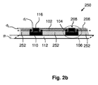
図2bは、照明アセンブリ250の断面を模式的に示す。照明アセンブリ250は、照明アセンブリ200に類似するが、LEDアセンブリ106のサブマウント110間に、二次熱材料252が配置される。二次熱材料252は、少なくともワイヤ102を封入し、一次熱層112に熱的に結合される。更なる実施形態では、図示されるように、二次熱材料252は、ワイヤ102とLEDアセンブリ106の電極との間の半田接合104も封入する。二次熱材料252は、熱伝導性の電気絶縁性材料である。二次熱材料252は、LEDダイ116から一次熱層112に向けた熱の熱伝導経路を提供する。従って、LEDダイ116のより多くの熱が一次熱層112に向けて伝導され、その為、冷却の向上がLEDダイ116に提供される。
FIG. 2 b schematically shows a cross section of the
図2bに示されるように、幅d1の間隙が二次熱材料252とLEDダイ116との間に存在する。サイズd1の間隙は、製造上の理由からのみ存在する必要がある。サイズd1の間隙は、LEDダイ116の側面に対する半田ワイヤ端のために必要とされる。距離d1は、少なくとも200マイクロメートルとする。
As shown in FIG. 2 b, a gap of width d 1 exists between the secondary
図2bでは、仮想線206も描かれている。仮想線206は、LEDダイ116の上面208によって形成される仮想面上の線である。二次熱材料252は、仮想線206によって模式的に示される仮想面の上方に延在せず、従って、仮想線206と二次熱材料252の上面との距離d2は、0以上である。二次熱材料252が、LEDダイ116の上面208の上方に延在しない場合、この材料は、LEDダイ116の発光を妨げない。二次熱材料252が光透過性(例えば透明又は半透明)である場合、二次熱材料は、その場合発光をあまり妨げないことから、仮想線206の上方に延在しても良い。
In FIG. 2b, an
ある実施形態では、二次熱材料は、熱伝導性粒子で充填されたシリコーンである。更なる実施形態では、熱伝導性粒子は、窒化ホウ素粒子である。窒化ホウ素粒子のサイズは、400ナノメートルから5マイクロメートルまでの範囲内とし、二次熱材料中の窒化ホウ素粒子の重量パーセントは、25〜35wt%の範囲内とする。窒化ホウ素粒子は、白色の外観を有し、その結果、この材料に衝突するLEDダイからの光を反射する。窒化ホウ素粒子は、照明アセンブリの光学効率に寄与する。窒化ホウ素粒子で充填されたシリコーンは、更に、熱的に比較的良好な黒体であり、これは、それが暖まると赤外線放射の形態で熱を放射する事を意味する。従って、二次熱材料252は、一次熱層112への熱伝導経路を提供するだけでなく、熱を照明アセンブリ250の周囲に伝達する。
In some embodiments, the secondary thermal material is silicone filled with thermally conductive particles. In a further embodiment, the thermally conductive particles are boron nitride particles. The size of the boron nitride particles is in the range of 400 nanometers to 5 micrometers, and the weight percent of the boron nitride particles in the secondary thermal material is in the range of 25 to 35 wt%. Boron nitride particles have a white appearance and consequently reflect light from the LED die that impinges on this material. Boron nitride particles contribute to the optical efficiency of the lighting assembly. Silicone filled with boron nitride particles is also a thermally relatively good black body, which means it emits heat in the form of infrared radiation when it warms. Thus, the secondary
別の実施形態では、熱伝導性粒子は、六方晶窒化ホウ素、アルミナ(Al2O3)、ZnO、又はTiO2を含む。 In another embodiment, the thermally conductive particles comprise hexagonal boron nitride, alumina (Al 2 O 3 ), ZnO, or TiO 2 .
一次熱層112は、銅の層でも良い。この層の厚さは、thで示される。一次熱層112は、LEDアセンブリ106から十分な熱を奪うことが可能であるためには、厚さが70マイクロメートルを超えるべきである。ある特定の実施形態では、一次熱層112は、厚さが1ミリメートルを超えるべきでない。一次熱層112が銅から成り、比較的小さな厚さを有する場合、それは、ある程度可撓性がある。同じ特定の実施形態において、二次熱材料が熱伝導性粒子を有するシリコーンから成る場合、照明アセンブリは、全体として比較的可撓性があり、曲面が発光する用途に使用され得る。
The primary
図3は、照明アセンブリ300の断面を模式的に示す。照明アセンブリ300は、図2bの照明アセンブリ250に類似するが、二次熱材料306が、LEDダイ116の上面208によって形成される仮想面を越えて延在する。この構成では、二次熱材料306は、LEDダイ116を含むキャビティ304の壁を形成する。ある有利な実施形態では、二次熱材料306は、キャビティ304の壁に衝突する光を反射するようなものである。キャビティ304は、光出射窓を有し、光出射窓には、特定の光学層302が設けられても良い。この特定の光学層302は、例えば、拡散層、カラーフィルタ、マイクロコリメータを備えた層、又は例えば発光材料を含む層である。発光材料は、LEDダイから受け取られた光の一部を吸収し、吸収された光の一部を別の色の光に変換する。
FIG. 3 schematically illustrates a cross section of the
図4は、本発明の第2の態様による光源400の断面を模式的に示す。光源400は、その断面が図4に示される光透過性チューブ402を含む。本発明の第1の態様による照明アセンブリは、チューブ402内のチューブ402の内面の一部上に設けられる。一次熱層112は、チューブがヒートシンクとして機能し得るように、チューブ402と接触させられる。一次熱層112は、可撓性があり、その為、チューブ402の曲面形状を辿る事ができる。LEDアセンブリ間のワイヤ102も湾曲していても良い。チューブ402は光透過性であり、これは、それが透明又は半透明でも良い事を意味する。
FIG. 4 schematically shows a cross section of a
光源400の形状は、光透過性チューブ402の示された形状に限定されないことに留意されたい。光源400の他の実施形態では、光源は、例えば従来の電球を含む。
Note that the shape of the
図5は、本発明の第3の態様による2つの照明器具を含む部屋の内部500を模式的に示す。天井502には、例えば図4に描写されたような複数の光源400を含む長方形の照明器具504が模式的に示されている。壁508には、例えば図2bの照明アセンブリ250を含む円形の照明器具506が模式的に描かれている。照明アセンブリ250が照明器具506に配置される場合は、一次熱層112は、照明器具506がヒートシンクとして機能するように、照明器具506の材料と接触させられ得る。
FIG. 5 schematically shows an interior 500 of a room including two luminaires according to the third aspect of the present invention. On the
上述の実施形態が、本発明を限定するのではなく例示し、当業者が添付の特許請求の範囲から逸脱することなく多くの代替実施形態を設計可能である事に留意されたい。 It should be noted that the above-described embodiments illustrate rather than limit the invention, and that many alternative embodiments can be designed by those skilled in the art without departing from the scope of the appended claims.
特許請求の範囲において、丸括弧内の何れの参照符号も特許請求の範囲を限定するものと解釈されるものではない。「含む(comprise)」という動詞及びその活用形の使用は、特許請求の範囲に記載されたもの以外の要素又はステップの存在を排除しない。要素に先行する冠詞「a」又は「an」は、複数のそのような要素の存在を排除しない。本発明は、幾つかの区別できる要素を含むハードウェアを用いて実施され得る。幾つかの手段を列挙する装置請求項では、これらの手段の幾つかは、ハードウェアの同一のアイテムによって具現化されても良い。特定の方策が互いに異なる従属請求項に記載されているという事実だけでは、これらの方策の組み合わせを有利に使用できないことを意味しない。 In the claims, any reference signs placed between parentheses shall not be construed as limiting the claim. Use of the verb “comprise” and its conjugations does not exclude the presence of elements or steps other than those listed in a claim. The article “a” or “an” preceding an element does not exclude the presence of a plurality of such elements. The present invention may be implemented using hardware that includes several distinct elements. In the device claim enumerating several means, several of these means may be embodied by one and the same item of hardware. The fact that specific measures are recited in mutually different dependent claims does not mean that a combination of these measures cannot be used to advantage.
Claims (15)
− 複数の発光ダイオードアセンブリと、
− 少なくとも2つの異なる発光ダイオードアセンブリの電極間に電気的に結合される複数のワイヤと、
を含む照明アセンブリであって、
前記発光ダイオードアセンブリは、
− 熱伝導性且つ電気絶縁性セラミックのサブマウントであって、前記一次熱層に熱的に結合される第1の面と、前記第1の面とは反対側の第2の面とを有するサブマウントと、
− 前記サブマウントの前記第2の面に配置される第1及び第2の金属電極と、
− 発光ダイオードのアノードを前記第1の金属電極に、及び前記発光ダイオードのカソードを前記第2の金属電極に電気的及び熱的に結合させた発光ダイオードダイと、
− 熱伝導性且つ電気絶縁性であり、前記一次熱層に熱的に結合された二次熱材料であって、前記複数のワイヤのサブセットを封入する為に、前記複数のサブマウントのサブセット間及び前記複数の発光ダイオードダイのサブセット間に配置され、前記発光ダイオードダイの上面によって形成される仮想面を越えて延在せず、前記発光ダイオードダイを含むキャビティの壁を形成する、二次熱材料と、
を含む、照明アセンブリ。 -A primary thermal layer of thermally conductive material;
-A plurality of light emitting diode assemblies;
A plurality of wires electrically coupled between electrodes of at least two different light emitting diode assemblies;
A lighting assembly comprising:
The light emitting diode assembly includes:
A thermally conductive and electrically insulating ceramic submount having a first surface thermally coupled to the primary thermal layer and a second surface opposite the first surface; A submount,
-First and second metal electrodes disposed on the second surface of the submount;
A light emitting diode die having an anode of a light emitting diode electrically and thermally coupled to the first metal electrode and a cathode of the light emitting diode to the second metal electrode;
-A thermally conductive and electrically insulating secondary thermal material thermally coupled to the primary thermal layer between the plurality of submount subsets to encapsulate the plurality of wire subsets; And a secondary heat disposed between a subset of the plurality of light emitting diode dies and not extending beyond a virtual plane formed by a top surface of the light emitting diode die and forming a wall of a cavity containing the light emitting diode die. Materials,
Including an illumination assembly.
Applications Claiming Priority (3)
| Application Number | Priority Date | Filing Date | Title |
|---|---|---|---|
| US201261582560P | 2012-01-03 | 2012-01-03 | |
| US61/582,560 | 2012-01-03 | ||
| PCT/IB2012/057596 WO2013102823A1 (en) | 2012-01-03 | 2012-12-21 | A lighting assembly, a light source and a luminaire |
Publications (3)
| Publication Number | Publication Date |
|---|---|
| JP2015507825A JP2015507825A (en) | 2015-03-12 |
| JP2015507825A5 JP2015507825A5 (en) | 2016-02-12 |
| JP6038175B2 true JP6038175B2 (en) | 2016-12-07 |
Family
ID=47747695
Family Applications (1)
| Application Number | Title | Priority Date | Filing Date |
|---|---|---|---|
| JP2014549599A Expired - Fee Related JP6038175B2 (en) | 2012-01-03 | 2012-12-21 | Lighting assembly, light source, and lighting fixture |
Country Status (5)
| Country | Link |
|---|---|
| US (1) | US9874316B2 (en) |
| EP (1) | EP2800925B1 (en) |
| JP (1) | JP6038175B2 (en) |
| CN (1) | CN104024722B (en) |
| WO (1) | WO2013102823A1 (en) |
Cited By (1)
| Publication number | Priority date | Publication date | Assignee | Title |
|---|---|---|---|---|
| US11217625B2 (en) | 2018-12-10 | 2022-01-04 | Samsung Electronics Co., Ltd. | Display module including micro light-emitting diodes and reflective layer, display apparatus including the same and method of manufacturing display module |
Families Citing this family (12)
| Publication number | Priority date | Publication date | Assignee | Title |
|---|---|---|---|---|
| DE102010026344A1 (en) * | 2010-07-07 | 2012-01-12 | Osram Opto Semiconductors Gmbh | led |
| WO2013030714A1 (en) * | 2011-08-29 | 2013-03-07 | Koninklijke Philips Electronics N.V. | A flexible lighting assembly, a luminaire, and a method of manufacturing a flexible layer |
| US9326338B2 (en) | 2013-06-21 | 2016-04-26 | Micron Technology, Inc. | Multi-junction solid state transducer devices for direct AC power and associated systems and methods |
| EP3066896A1 (en) | 2013-11-05 | 2016-09-14 | Philips Lighting Holding B.V. | Assembly and method of manufacturing an assembly |
| US10024530B2 (en) * | 2014-07-03 | 2018-07-17 | Sansi Led Lighting Inc. | Lighting device and LED luminaire |
| CN104302102A (en) * | 2014-09-26 | 2015-01-21 | 中国科学院长春光学精密机械与物理研究所 | Infrared focal plane sensor non-packaging application method |
| DE102015106444A1 (en) * | 2015-04-27 | 2016-10-27 | Osram Opto Semiconductors Gmbh | Optoelectronic component arrangement and method for producing a multiplicity of optoelectronic component arrangements |
| US20190120444A1 (en) * | 2015-12-18 | 2019-04-25 | Applied Electronic Materials, LLC | Modular lighting system including light modules with integrated led units |
| US10941926B2 (en) | 2015-12-18 | 2021-03-09 | Applied Electronic Materials, LLC | Modular lighting system including light modules with integrated LED units |
| US10660238B2 (en) | 2017-09-21 | 2020-05-19 | Avx Corporation | Electrically insulating thermal connector having a low thermal resistivity |
| RU2689301C1 (en) * | 2018-03-13 | 2019-05-27 | Анатолий Павлович Бежко | Light-emitting diode module for lighting fixture |
| US11293627B1 (en) * | 2021-02-02 | 2022-04-05 | Gary Lagasse | Miniature LED lightbulb mounting device |
Family Cites Families (24)
| Publication number | Priority date | Publication date | Assignee | Title |
|---|---|---|---|---|
| JP4646357B2 (en) | 2000-06-08 | 2011-03-09 | 東レ・ダウコーニング株式会社 | Thermally conductive silicone rubber composition |
| KR101047246B1 (en) * | 2002-07-25 | 2011-07-06 | 조나단 에스. 담 | Method and apparatus for using curing LED |
| EP1590994B1 (en) * | 2003-02-07 | 2016-05-18 | Panasonic Intellectual Property Management Co., Ltd. | Metal base wiring board for retaining light emitting elements, light emitting source, lighting apparatus, and display apparatus |
| US10376711B2 (en) * | 2003-03-14 | 2019-08-13 | Light Sciences Oncology Inc. | Light generating guide wire for intravascular use |
| TWI224661B (en) | 2003-06-13 | 2004-12-01 | Yuan Lin | Multi-channel light source based longitudinal lighting device |
| JP4192742B2 (en) * | 2003-09-30 | 2008-12-10 | 豊田合成株式会社 | Light emitting device |
| JP2006019319A (en) * | 2004-06-30 | 2006-01-19 | C I Kasei Co Ltd | Light-emitting diode assembly body and manufacturing method thereof |
| US7303315B2 (en) * | 2004-11-05 | 2007-12-04 | 3M Innovative Properties Company | Illumination assembly using circuitized strips |
| EP1875519A2 (en) | 2005-03-30 | 2008-01-09 | Koninklijke Philips Electronics N.V. | Flexible led array |
| US20060289887A1 (en) | 2005-06-24 | 2006-12-28 | Jabil Circuit, Inc. | Surface mount light emitting diode (LED) assembly with improved power dissipation |
| KR101241650B1 (en) | 2005-10-19 | 2013-03-08 | 엘지이노텍 주식회사 | Package of light emitting diode |
| US7710045B2 (en) | 2006-03-17 | 2010-05-04 | 3M Innovative Properties Company | Illumination assembly with enhanced thermal conductivity |
| KR101412473B1 (en) | 2006-04-25 | 2014-06-30 | 코닌클리케 필립스 엔.브이. | Led array grid, method and device for manufacturing said grid and led component for use in the same |
| CN101517755A (en) * | 2006-09-21 | 2009-08-26 | 3M创新有限公司 | Thermally conductive LED assembly |
| US8581393B2 (en) | 2006-09-21 | 2013-11-12 | 3M Innovative Properties Company | Thermally conductive LED assembly |
| TWM331086U (en) * | 2007-10-17 | 2008-04-21 | Tai Sol Electronics Co Ltd | Combination of LED and heat conduction device |
| KR100917712B1 (en) | 2007-12-13 | 2009-09-21 | 유트로닉스주식회사 | LED array module using aluminum metal substrate |
| US8067782B2 (en) | 2008-04-08 | 2011-11-29 | Advanced Optoelectric Technology, Inc. | LED package and light source device using same |
| KR100982986B1 (en) * | 2008-04-17 | 2010-09-17 | 삼성엘이디 주식회사 | Submount, LED Package and Manufacturing Method Thereof |
| JP5146356B2 (en) * | 2009-02-24 | 2013-02-20 | 豊田合成株式会社 | Light emitting device and manufacturing method thereof |
| CN101894901B (en) * | 2009-04-08 | 2013-11-20 | 硅谷光擎 | Package for multiple light emitting diodes |
| US8348460B2 (en) * | 2009-05-01 | 2013-01-08 | Abl Ip Holding Llc | Lighting apparatus with several light units arranged in a heatsink |
| CN101929624A (en) * | 2009-06-25 | 2010-12-29 | 富士迈半导体精密工业(上海)有限公司 | Lighting device |
| CN201502903U (en) | 2009-09-29 | 2010-06-09 | 深圳市庄正电子技术有限公司 | LED light source structure used for projection equipment |
-
2012
- 2012-12-21 US US14/370,345 patent/US9874316B2/en not_active Expired - Fee Related
- 2012-12-21 EP EP12826553.5A patent/EP2800925B1/en not_active Not-in-force
- 2012-12-21 JP JP2014549599A patent/JP6038175B2/en not_active Expired - Fee Related
- 2012-12-21 CN CN201280065600.5A patent/CN104024722B/en not_active Expired - Fee Related
- 2012-12-21 WO PCT/IB2012/057596 patent/WO2013102823A1/en active Application Filing
Cited By (1)
| Publication number | Priority date | Publication date | Assignee | Title |
|---|---|---|---|---|
| US11217625B2 (en) | 2018-12-10 | 2022-01-04 | Samsung Electronics Co., Ltd. | Display module including micro light-emitting diodes and reflective layer, display apparatus including the same and method of manufacturing display module |
Also Published As
| Publication number | Publication date |
|---|---|
| US20140369045A1 (en) | 2014-12-18 |
| JP2015507825A (en) | 2015-03-12 |
| EP2800925B1 (en) | 2015-07-08 |
| CN104024722A (en) | 2014-09-03 |
| EP2800925A1 (en) | 2014-11-12 |
| CN104024722B (en) | 2018-03-06 |
| WO2013102823A1 (en) | 2013-07-11 |
| US9874316B2 (en) | 2018-01-23 |
Similar Documents
| Publication | Publication Date | Title |
|---|---|---|
| JP6038175B2 (en) | Lighting assembly, light source, and lighting fixture | |
| JP5082083B2 (en) | LED lighting device | |
| JP4880358B2 (en) | Light source substrate and illumination device using the same | |
| JP5029822B2 (en) | Light source and lighting device | |
| TWI683458B (en) | Peripheral heat sinking arrangement for high brightness light emitting devices | |
| TW201326663A (en) | LED packages for an LED bulb | |
| JP2010003674A (en) | Light source unit, and lighting apparatus | |
| US8801238B2 (en) | Light-emitting device | |
| JP2007324547A (en) | Light emitting diode light source, illuminator, display unit, and traffic signal | |
| JP2008071895A (en) | Lighting system | |
| EP3091279A1 (en) | Led light source heat dissipation structure and heat dissipation method thereof | |
| JP5131668B2 (en) | LED lighting device | |
| US20140211475A1 (en) | Light bulb | |
| WO2016029808A1 (en) | Light emission and heat dissipation structure of led light source and light emission and heat dissipation method therefor | |
| JP6495307B2 (en) | LED lighting device | |
| JP2013236047A (en) | Integral high efficiency multilayer type lighting device | |
| JP2012156476A (en) | Light source module and manufacturing method thereof | |
| JP5569759B2 (en) | Light source unit | |
| JP6085459B2 (en) | Lighting device | |
| TWI412700B (en) | Thermal resistance parallel LED light source and contains the thermal resistance of parallel LED light source lamps | |
| JP6806925B2 (en) | Manufacturing method of solid-state light emitter package, lamp, luminaire, and solid-state light emitter package | |
| TWI476968B (en) | Light-emitting device | |
| JP5582365B2 (en) | Lighting device | |
| TW201636546A (en) | Car lamp device | |
| TWI390761B (en) | Light emitting diode package |
Legal Events
| Date | Code | Title | Description |
|---|---|---|---|
| A521 | Request for written amendment filed |
Free format text: JAPANESE INTERMEDIATE CODE: A523 Effective date: 20151217 |
|
| A621 | Written request for application examination |
Free format text: JAPANESE INTERMEDIATE CODE: A621 Effective date: 20151217 |
|
| A711 | Notification of change in applicant |
Free format text: JAPANESE INTERMEDIATE CODE: A711 Effective date: 20160927 |
|
| A977 | Report on retrieval |
Free format text: JAPANESE INTERMEDIATE CODE: A971007 Effective date: 20160928 |
|
| TRDD | Decision of grant or rejection written | ||
| A01 | Written decision to grant a patent or to grant a registration (utility model) |
Free format text: JAPANESE INTERMEDIATE CODE: A01 Effective date: 20161004 |
|
| A61 | First payment of annual fees (during grant procedure) |
Free format text: JAPANESE INTERMEDIATE CODE: A61 Effective date: 20161101 |
|
| R150 | Certificate of patent or registration of utility model |
Ref document number: 6038175 Country of ref document: JP Free format text: JAPANESE INTERMEDIATE CODE: R150 |
|
| S531 | Written request for registration of change of domicile |
Free format text: JAPANESE INTERMEDIATE CODE: R313531 |
|
| S533 | Written request for registration of change of name |
Free format text: JAPANESE INTERMEDIATE CODE: R313533 |
|
| R350 | Written notification of registration of transfer |
Free format text: JAPANESE INTERMEDIATE CODE: R350 |
|
| R250 | Receipt of annual fees |
Free format text: JAPANESE INTERMEDIATE CODE: R250 |
|
| LAPS | Cancellation because of no payment of annual fees |