JP6027059B2 - メモリ内のデータを管理するための方法および装置 - Google Patents
メモリ内のデータを管理するための方法および装置 Download PDFInfo
- Publication number
- JP6027059B2 JP6027059B2 JP2014144986A JP2014144986A JP6027059B2 JP 6027059 B2 JP6027059 B2 JP 6027059B2 JP 2014144986 A JP2014144986 A JP 2014144986A JP 2014144986 A JP2014144986 A JP 2014144986A JP 6027059 B2 JP6027059 B2 JP 6027059B2
- Authority
- JP
- Japan
- Prior art keywords
- memory cell
- programmed
- cell
- state
- charge
- Prior art date
- Legal status (The legal status is an assumption and is not a legal conclusion. Google has not performed a legal analysis and makes no representation as to the accuracy of the status listed.)
- Expired - Fee Related
Links
- 230000015654 memory Effects 0.000 title claims description 154
- 238000000034 method Methods 0.000 title claims description 18
- 230000008672 reprogramming Effects 0.000 claims description 29
- 230000006870 function Effects 0.000 claims description 10
- 239000007787 solid Substances 0.000 claims description 9
- 230000004044 response Effects 0.000 claims description 6
- 238000012546 transfer Methods 0.000 claims description 5
- 230000008859 change Effects 0.000 claims description 4
- 238000009529 body temperature measurement Methods 0.000 claims description 3
- 238000009826 distribution Methods 0.000 description 45
- 238000003860 storage Methods 0.000 description 12
- 238000013500 data storage Methods 0.000 description 10
- 230000003321 amplification Effects 0.000 description 6
- 238000003199 nucleic acid amplification method Methods 0.000 description 6
- 230000008569 process Effects 0.000 description 5
- 230000000694 effects Effects 0.000 description 4
- 230000015556 catabolic process Effects 0.000 description 3
- 238000012937 correction Methods 0.000 description 3
- 238000006731 degradation reaction Methods 0.000 description 3
- 238000010586 diagram Methods 0.000 description 3
- 238000012545 processing Methods 0.000 description 3
- 239000004065 semiconductor Substances 0.000 description 3
- 239000000758 substrate Substances 0.000 description 3
- 238000009825 accumulation Methods 0.000 description 2
- 239000003990 capacitor Substances 0.000 description 2
- 238000004891 communication Methods 0.000 description 2
- 230000001186 cumulative effect Effects 0.000 description 2
- 230000005347 demagnetization Effects 0.000 description 2
- 238000001514 detection method Methods 0.000 description 2
- 238000007726 management method Methods 0.000 description 2
- 230000007246 mechanism Effects 0.000 description 2
- 238000011084 recovery Methods 0.000 description 2
- 230000007704 transition Effects 0.000 description 2
- 238000003491 array Methods 0.000 description 1
- 230000002457 bidirectional effect Effects 0.000 description 1
- 230000005684 electric field Effects 0.000 description 1
- 230000007613 environmental effect Effects 0.000 description 1
- 238000011156 evaluation Methods 0.000 description 1
- 230000014759 maintenance of location Effects 0.000 description 1
- 238000004519 manufacturing process Methods 0.000 description 1
- 238000005259 measurement Methods 0.000 description 1
- 238000004242 micellar liquid chromatography Methods 0.000 description 1
- 230000000737 periodic effect Effects 0.000 description 1
- 238000012360 testing method Methods 0.000 description 1
Images


Classifications
-
- G—PHYSICS
- G11—INFORMATION STORAGE
- G11C—STATIC STORES
- G11C16/00—Erasable programmable read-only memories
- G11C16/02—Erasable programmable read-only memories electrically programmable
- G11C16/06—Auxiliary circuits, e.g. for writing into memory
- G11C16/10—Programming or data input circuits
- G11C16/14—Circuits for erasing electrically, e.g. erase voltage switching circuits
-
- G—PHYSICS
- G11—INFORMATION STORAGE
- G11C—STATIC STORES
- G11C11/00—Digital stores characterised by the use of particular electric or magnetic storage elements; Storage elements therefor
- G11C11/56—Digital stores characterised by the use of particular electric or magnetic storage elements; Storage elements therefor using storage elements with more than two stable states represented by steps, e.g. of voltage, current, phase, frequency
- G11C11/5621—Digital stores characterised by the use of particular electric or magnetic storage elements; Storage elements therefor using storage elements with more than two stable states represented by steps, e.g. of voltage, current, phase, frequency using charge storage in a floating gate
- G11C11/5628—Programming or writing circuits; Data input circuits
-
- G—PHYSICS
- G11—INFORMATION STORAGE
- G11C—STATIC STORES
- G11C16/00—Erasable programmable read-only memories
- G11C16/02—Erasable programmable read-only memories electrically programmable
- G11C16/04—Erasable programmable read-only memories electrically programmable using variable threshold transistors, e.g. FAMOS
- G11C16/0483—Erasable programmable read-only memories electrically programmable using variable threshold transistors, e.g. FAMOS comprising cells having several storage transistors connected in series
-
- G—PHYSICS
- G11—INFORMATION STORAGE
- G11C—STATIC STORES
- G11C16/00—Erasable programmable read-only memories
- G11C16/02—Erasable programmable read-only memories electrically programmable
- G11C16/06—Auxiliary circuits, e.g. for writing into memory
- G11C16/10—Programming or data input circuits
-
- G—PHYSICS
- G11—INFORMATION STORAGE
- G11C—STATIC STORES
- G11C16/00—Erasable programmable read-only memories
- G11C16/02—Erasable programmable read-only memories electrically programmable
- G11C16/06—Auxiliary circuits, e.g. for writing into memory
- G11C16/34—Determination of programming status, e.g. threshold voltage, overprogramming or underprogramming, retention
- G11C16/3418—Disturbance prevention or evaluation; Refreshing of disturbed memory data
- G11C16/3431—Circuits or methods to detect disturbed nonvolatile memory cells, e.g. which still read as programmed but with threshold less than the program verify threshold or read as erased but with threshold greater than the erase verify threshold, and to reverse the disturbance via a refreshing programming or erasing step
-
- G—PHYSICS
- G11—INFORMATION STORAGE
- G11C—STATIC STORES
- G11C13/00—Digital stores characterised by the use of storage elements not covered by groups G11C11/00, G11C23/00, or G11C25/00
- G11C13/0002—Digital stores characterised by the use of storage elements not covered by groups G11C11/00, G11C23/00, or G11C25/00 using resistive RAM [RRAM] elements
- G11C13/0021—Auxiliary circuits
- G11C13/0033—Disturbance prevention or evaluation; Refreshing of disturbed memory data
-
- G—PHYSICS
- G11—INFORMATION STORAGE
- G11C—STATIC STORES
- G11C13/00—Digital stores characterised by the use of storage elements not covered by groups G11C11/00, G11C23/00, or G11C25/00
- G11C13/0002—Digital stores characterised by the use of storage elements not covered by groups G11C11/00, G11C23/00, or G11C25/00 using resistive RAM [RRAM] elements
- G11C13/0021—Auxiliary circuits
- G11C13/0069—Writing or programming circuits or methods
Landscapes
- Engineering & Computer Science (AREA)
- Microelectronics & Electronic Packaging (AREA)
- Computer Hardware Design (AREA)
- Read Only Memory (AREA)
Description
本開示のさまざまな実施の形態は概してフラッシュメモリアレイ等のメモリ内のデータの管理に関する。
本開示は概して、データ記憶装置のフラッシュメモリアレイ等であるがこれに限定されないメモリモジュールに格納されたデータの管理に関する。
Claims (19)
- 一組のソリッドステート不揮発性メモリセルに、前記組の中の各メモリセルが書込により関連する初期プログラム状態になるように、データを書込むステップと、
前記組の中の選択されたメモリセルのプログラム状態のドリフトを検出するステップと、
前記選択されたメモリセルを部分的に再プログラムして前記選択されたメモリセルを前記関連する初期プログラム状態に戻すステップとを含み、前記組の中の少なくとも1つのその他のメモリセルは部分的に再プログラムされず、
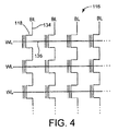
電荷の複数の増分を与えて前記選択されたメモリセルを前記初期プログラム状態にプログラムし、その後、電荷の、より小さい複数の増分を与えて前記選択されたメモリセルを部分的に再プログラムして前記初期プログラム状態に戻す、方法。 - 前記一組のソリッドステート不揮発性メモリセルは、各フラッシュメモリセルのフローティングゲートに電荷を蓄積することにより1ページ分のデータを同時に格納することによってプログラムされる一行のフラッシュメモリセルを含む、請求項1に記載の方法。
- 前記フラッシュメモリセルは各々、2ページ分のデータが前記メモリセルによって格納されるように、マルチレベルセル(MLC)として構成される、請求項2に記載の方法。
- 第1の書込パルス幅を与えることによって、各メモリセルを前記関連する初期プログラム状態にプログラムし、その後第2の書込パルス幅を与えることによって、選択されたメモリセルをその関連するプログラム状態に再プログラムし、前記第2の書込パルス幅は前記第1の書込パルス幅よりも短い、請求項1から請求項3のいずれか1項に記載の方法。
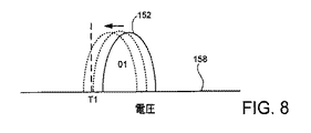
- 前記プログラム状態のドリフトは、電圧しきい値を選択されたメモリセルに与えることによって検出される、請求項1に記載の方法。
- 前記プログラム状態のドリフトは、選択されたメモリセルに関連するビットエラーレート(BER)に応じて検出される、請求項1に記載の方法。
- 前記プログラム状態のドリフトは、選択されたメモリセルが前記関連する初期プログラム状態にプログラムされてから経過した時間に応じて検出される、請求項1に記載の方法。
- 前記プログラム状態のドリフトは、選択されたメモリセルに関連する温度測定値に応じて検出される、請求項1に記載の方法。
- 前記メモリセルは、抵抗ランダムアクセスメモリ(RRAM(登録商標))セル、相変化ランダムアクセスメモリ(PCRAM)セル、またはスピントルクトランスファーランダムアクセスメモリ(STRAM)セルのうちの選択されたいずれか1つである、請求項1に記載の方法。
- 前記選択されたメモリセルを、再プログラムされたものとして、前記選択されたメモリセルに関連する制御データにマークするステップをさらに含む、請求項1から請求項9のいずれか1項に記載の方法。
- アドレス可能な単位になるように配列されたソリッドステート不揮発性メモリセルのアレイと、
メモリの選択されたアドレス可能単位に、前記選択されたアドレス可能単位の中の各メモリセルが関連する初期プログラム状態を有するように、データを書込むようにされた書込回路と、
前記選択されたアドレス可能単位の中のメモリセルのうちの少なくとも1つのプログラム状態のドリフトを検出するように、かつ、前記選択されたアドレス可能単位の中の全メモリセルよりも少ないメモリセルを部分的に再プログラムして前記関連する初期プログラム状態にすることを前記書込回路に指示するようにされた、部分再プログラミング回路とを備え、
前記部分再プログラミング回路は、前記選択されたメモリセルの消去を挟まずに、前記初期プログラム状態にプログラムした際の複数の電荷の増分よりも小さい、複数の電荷の増分を与えて前記選択されたメモリセルを部分的に再プログラムして前記初期プログラム状態に戻す、装置。 - 前記選択されたアドレス可能単位は、1行のフラッシュメモリセルであり、前記書込回路は、前記フラッシュメモリセルに電荷の第1の増分を蓄積し移動することによって1ページのデータを前記行に書込み、前記書込回路は、前記電荷の第1の増分よりも小さい電荷の第2の増分を蓄積し移動することによって前記行の前記フラッシュメモリセルを部分的に再プログラムする、請求項11に記載の装置。
- 第1の書込パルス幅を与えることによって、各メモリセルを前記関連する初期プログラム状態にプログラムし、その後第2の書込パルス幅を与えることによって、選択されたメモリセルをその関連するプログラム状態に再プログラムし、前記第2の書込パルス幅は前記第1の書込パルス幅よりも短い、請求項11または請求項12に記載の装置。
- 前記プログラム状態のドリフトは、電圧しきい値を選択されたメモリセルに与えることによって検出される、請求項11に記載の装置。
- 前記プログラム状態のドリフトは、選択されたメモリセルに関連するビットエラーレート(BER)に応じて検出される、請求項11に記載の装置。
- 前記プログラム状態のドリフトは、選択されたメモリセルが前記関連する初期プログラム状態にプログラムされてから経過した時間に応じて検出される、請求項11に記載の装置。
- 前記プログラム状態のドリフトは、選択されたメモリセルに関連する温度測定値に応じて検出される、請求項11に記載の装置。
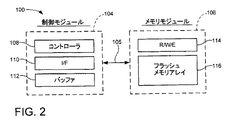
- 一単位として消去され割当てられる複数のガーベジコレクション単位(GCU)になるように配列された不揮発性フラッシュメモリセルを含むフラッシュメモリアレイと、
選択されたGCUからデータを読出し選択されたGCUにデータを書込み選択されたGCUを消去するようにされた、読出/書込/消去(R/W/E)回路と、
前記選択されたGCUの中のプログラムされた一組のフラッシュメモリセルをプログラミングドリフトが生じたものであると識別し、かつ、前記プログラムされた一組のフラッシュメモリセルを部分的に再プログラムすることで電荷を前記メモリセルに移動させて前記メモリセルを前記選択されたGCUの消去を挟まずにその初期プログラム状態に戻すことを前記R/W/E回路に指示する、部分再プログラミング回路とを備え、
電荷の複数の増分を与えて、選択されたメモリセルを前記初期プログラム状態にプログラムし、その後、電荷の、より小さい複数の増分を与えて前記選択されたメモリセルを部分的に再プログラムして前記初期プログラム状態に戻す、装置。 - 前記部分再プログラミング回路はさらに、前記部分的に再プログラムする動作の前に1つ以上の電圧しきい値を前記プログラムされた一組のフラッシュメモリセルに与えて各々のプログラム状態を評価することを前記R/W/E回路に指示する、請求項18に記載の装置。
Applications Claiming Priority (2)
| Application Number | Priority Date | Filing Date | Title |
|---|---|---|---|
| US13/943,441 | 2013-07-16 | ||
| US13/943,441 US9378830B2 (en) | 2013-07-16 | 2013-07-16 | Partial reprogramming of solid-state non-volatile memory cells |
Publications (3)
| Publication Number | Publication Date |
|---|---|
| JP2015022788A JP2015022788A (ja) | 2015-02-02 |
| JP2015022788A5 JP2015022788A5 (ja) | 2015-03-12 |
| JP6027059B2 true JP6027059B2 (ja) | 2016-11-16 |
Family
ID=52343461
Family Applications (1)
| Application Number | Title | Priority Date | Filing Date |
|---|---|---|---|
| JP2014144986A Expired - Fee Related JP6027059B2 (ja) | 2013-07-16 | 2014-07-15 | メモリ内のデータを管理するための方法および装置 |
Country Status (4)
| Country | Link |
|---|---|
| US (1) | US9378830B2 (ja) |
| JP (1) | JP6027059B2 (ja) |
| KR (2) | KR20150009478A (ja) |
| CN (1) | CN104332178B (ja) |
Families Citing this family (57)
| Publication number | Priority date | Publication date | Assignee | Title |
|---|---|---|---|---|
| US8738841B2 (en) | 2007-12-27 | 2014-05-27 | Sandisk Enterprise IP LLC. | Flash memory controller and system including data pipelines incorporating multiple buffers |
| US9699263B1 (en) | 2012-08-17 | 2017-07-04 | Sandisk Technologies Llc. | Automatic read and write acceleration of data accessed by virtual machines |
| US9501398B2 (en) | 2012-12-26 | 2016-11-22 | Sandisk Technologies Llc | Persistent storage device with NVRAM for staging writes |
| US9612948B2 (en) | 2012-12-27 | 2017-04-04 | Sandisk Technologies Llc | Reads and writes between a contiguous data block and noncontiguous sets of logical address blocks in a persistent storage device |
| US9454420B1 (en) | 2012-12-31 | 2016-09-27 | Sandisk Technologies Llc | Method and system of reading threshold voltage equalization |
| US9870830B1 (en) | 2013-03-14 | 2018-01-16 | Sandisk Technologies Llc | Optimal multilevel sensing for reading data from a storage medium |
| US9244763B1 (en) | 2013-03-15 | 2016-01-26 | Sandisk Enterprise Ip Llc | System and method for updating a reading threshold voltage based on symbol transition information |
| US9367246B2 (en) | 2013-03-15 | 2016-06-14 | Sandisk Technologies Inc. | Performance optimization of data transfer for soft information generation |
| US9384126B1 (en) | 2013-07-25 | 2016-07-05 | Sandisk Technologies Inc. | Methods and systems to avoid false negative results in bloom filters implemented in non-volatile data storage systems |
| US9524235B1 (en) | 2013-07-25 | 2016-12-20 | Sandisk Technologies Llc | Local hash value generation in non-volatile data storage systems |
| US9639463B1 (en) | 2013-08-26 | 2017-05-02 | Sandisk Technologies Llc | Heuristic aware garbage collection scheme in storage systems |
| US9361221B1 (en) * | 2013-08-26 | 2016-06-07 | Sandisk Technologies Inc. | Write amplification reduction through reliable writes during garbage collection |
| US9298608B2 (en) | 2013-10-18 | 2016-03-29 | Sandisk Enterprise Ip Llc | Biasing for wear leveling in storage systems |
| US9442662B2 (en) | 2013-10-18 | 2016-09-13 | Sandisk Technologies Llc | Device and method for managing die groups |
| US9436831B2 (en) | 2013-10-30 | 2016-09-06 | Sandisk Technologies Llc | Secure erase in a memory device |
| US9703816B2 (en) | 2013-11-19 | 2017-07-11 | Sandisk Technologies Llc | Method and system for forward reference logging in a persistent datastore |
| US9520197B2 (en) | 2013-11-22 | 2016-12-13 | Sandisk Technologies Llc | Adaptive erase of a storage device |
| US9520162B2 (en) | 2013-11-27 | 2016-12-13 | Sandisk Technologies Llc | DIMM device controller supervisor |
| US9582058B2 (en) | 2013-11-29 | 2017-02-28 | Sandisk Technologies Llc | Power inrush management of storage devices |
| US9703636B2 (en) | 2014-03-01 | 2017-07-11 | Sandisk Technologies Llc | Firmware reversion trigger and control |
| US9390814B2 (en) | 2014-03-19 | 2016-07-12 | Sandisk Technologies Llc | Fault detection and prediction for data storage elements |
| US9454448B2 (en) | 2014-03-19 | 2016-09-27 | Sandisk Technologies Llc | Fault testing in storage devices |
| US9448876B2 (en) | 2014-03-19 | 2016-09-20 | Sandisk Technologies Llc | Fault detection and prediction in storage devices |
| US9626399B2 (en) | 2014-03-31 | 2017-04-18 | Sandisk Technologies Llc | Conditional updates for reducing frequency of data modification operations |
| US9390021B2 (en) | 2014-03-31 | 2016-07-12 | Sandisk Technologies Llc | Efficient cache utilization in a tiered data structure |
| US9626400B2 (en) | 2014-03-31 | 2017-04-18 | Sandisk Technologies Llc | Compaction of information in tiered data structure |
| US9697267B2 (en) | 2014-04-03 | 2017-07-04 | Sandisk Technologies Llc | Methods and systems for performing efficient snapshots in tiered data structures |
| US10372613B2 (en) | 2014-05-30 | 2019-08-06 | Sandisk Technologies Llc | Using sub-region I/O history to cache repeatedly accessed sub-regions in a non-volatile storage device |
| US10146448B2 (en) | 2014-05-30 | 2018-12-04 | Sandisk Technologies Llc | Using history of I/O sequences to trigger cached read ahead in a non-volatile storage device |
| US10114557B2 (en) | 2014-05-30 | 2018-10-30 | Sandisk Technologies Llc | Identification of hot regions to enhance performance and endurance of a non-volatile storage device |
| US10656840B2 (en) | 2014-05-30 | 2020-05-19 | Sandisk Technologies Llc | Real-time I/O pattern recognition to enhance performance and endurance of a storage device |
| US9703491B2 (en) | 2014-05-30 | 2017-07-11 | Sandisk Technologies Llc | Using history of unaligned writes to cache data and avoid read-modify-writes in a non-volatile storage device |
| US10656842B2 (en) | 2014-05-30 | 2020-05-19 | Sandisk Technologies Llc | Using history of I/O sizes and I/O sequences to trigger coalesced writes in a non-volatile storage device |
| US10162748B2 (en) | 2014-05-30 | 2018-12-25 | Sandisk Technologies Llc | Prioritizing garbage collection and block allocation based on I/O history for logical address regions |
| US9652381B2 (en) | 2014-06-19 | 2017-05-16 | Sandisk Technologies Llc | Sub-block garbage collection |
| US9443601B2 (en) | 2014-09-08 | 2016-09-13 | Sandisk Technologies Llc | Holdup capacitor energy harvesting |
| US9576649B2 (en) * | 2015-03-31 | 2017-02-21 | Seagate Technology Llc | Charge loss compensation through augmentation of accumulated charge in a memory cell |
| KR102449337B1 (ko) * | 2015-12-14 | 2022-10-04 | 삼성전자주식회사 | 불휘발성 메모리 시스템의 동작 방법 |
| US10254969B2 (en) * | 2016-05-13 | 2019-04-09 | Seagate Technology Llc | Data refresh in flash memory |
| KR102565888B1 (ko) | 2016-09-12 | 2023-08-11 | 에스케이하이닉스 주식회사 | 반도체 메모리 장치 및 그것의 동작 방법 |
| US9952944B1 (en) | 2016-10-25 | 2018-04-24 | Sandisk Technologies Llc | First read solution for memory |
| US10262743B2 (en) * | 2016-10-25 | 2019-04-16 | Sandisk Technologies Llc | Command sequence for first read solution for memory |
| US10026486B1 (en) | 2017-03-06 | 2018-07-17 | Sandisk Technologies Llc | First read countermeasures in memory |
| CN108694979B (zh) * | 2017-04-06 | 2023-08-01 | 群联电子股份有限公司 | 数据写入方法、存储器控制电路单元与存储器存储装置 |
| US10347315B2 (en) | 2017-10-31 | 2019-07-09 | Sandisk Technologies Llc | Group read refresh |
| US10706920B2 (en) | 2017-11-02 | 2020-07-07 | Samsung Electronics Co., Ltd. | Memory device |
| KR102467075B1 (ko) | 2017-11-13 | 2022-11-11 | 삼성전자주식회사 | 메모리 장치 및 그의 리클레임 방법 |
| US10446246B2 (en) * | 2018-03-14 | 2019-10-15 | Silicon Storage Technology, Inc. | Method and apparatus for data refresh for analog non-volatile memory in deep learning neural network |
| US10733104B2 (en) * | 2018-08-03 | 2020-08-04 | Micron Technology, Inc. | Fast non-volatile storage device recovery techniques |
| KR102651129B1 (ko) | 2018-12-21 | 2024-03-26 | 삼성전자주식회사 | 메모리 장치의 데이터 재기입 방법, 상기 메모리 장치를 제어하는 메모리 컨트롤러 및 상기 메모리 컨트롤러의 제어 방법 |
| KR102161833B1 (ko) * | 2018-12-31 | 2020-10-05 | 성균관대학교산학협력단 | 온도 정보를 활용한 멀티 레벨 셀 상변화 메모리 스크러빙 장치 |
| DE102019203351A1 (de) * | 2019-03-12 | 2020-09-17 | Robert Bosch Gmbh | Verfahren und Vorrichtung zum Betreiben einer nichtflüchtigen Speichereinrichtung |
| US11061768B1 (en) * | 2020-02-14 | 2021-07-13 | Western Digital Technologies, Inc. | Storage device with increased endurance |
| JP2023079292A (ja) * | 2021-11-29 | 2023-06-08 | ラピステクノロジー株式会社 | 半導体記憶装置、データ書込方法及び半導体記憶装置の製造方法 |
| EP4441740A4 (en) | 2021-12-02 | 2025-06-18 | Yangtze Memory Technologies Co., Ltd. | MEMORY DEVICE, MEMORY SYSTEM, AND ASSOCIATED PROGRAM OPERATING METHOD |
| CN114400035A (zh) * | 2021-12-02 | 2022-04-26 | 长江存储科技有限责任公司 | 存储器的编程方法、存储器及存储系统 |
| US12360891B2 (en) * | 2023-02-22 | 2025-07-15 | Micron Technology, Inc. | Memory system host data reset function |
Family Cites Families (19)
| Publication number | Priority date | Publication date | Assignee | Title |
|---|---|---|---|---|
| US5815439A (en) | 1996-04-30 | 1998-09-29 | Agate Semiconductor, Inc. | Stabilization circuits and techniques for storage and retrieval of single or multiple digital bits per memory cell |
| US6343033B1 (en) * | 2000-02-25 | 2002-01-29 | Advanced Micro Devices, Inc. | Variable pulse width memory programming |
| US6424569B1 (en) * | 2000-02-25 | 2002-07-23 | Advanced Micro Devices, Inc. | User selectable cell programming |
| US7184307B2 (en) | 2001-08-28 | 2007-02-27 | Samsung Electronics Co., Ltd. | Flash memory device capable of preventing program disturbance according to partial programming |
| US6751146B1 (en) * | 2003-01-07 | 2004-06-15 | Advanced Micro Devices, Inc. | System and method for charge restoration in a non-volatile memory device |
| JP2004259144A (ja) * | 2003-02-27 | 2004-09-16 | Renesas Technology Corp | 半導体記憶装置 |
| DE102005009700B4 (de) * | 2004-02-26 | 2009-02-05 | Samsung Electronics Co., Ltd., Suwon | Programmierverfahren und nichtflüchtiger Speicher |
| US7325090B2 (en) | 2004-04-29 | 2008-01-29 | Sandisk Il Ltd. | Refreshing data stored in a flash memory |
| JP2007058966A (ja) * | 2005-08-23 | 2007-03-08 | Renesas Technology Corp | 半導体装置 |
| JP2009536423A (ja) | 2006-05-05 | 2009-10-08 | ハネウェル・インターナショナル・インコーポレーテッド | 不揮発性メモリをリフレッシュする方法 |
| KR100816162B1 (ko) * | 2007-01-23 | 2008-03-21 | 주식회사 하이닉스반도체 | 낸드 플래시 메모리 장치 및 셀 특성 개선 방법 |
| WO2009042298A1 (en) | 2007-09-26 | 2009-04-02 | Rambus Inc. | Flash memory refresh |
| US8938655B2 (en) * | 2007-12-20 | 2015-01-20 | Spansion Llc | Extending flash memory data retension via rewrite refresh |
| KR101406279B1 (ko) * | 2007-12-20 | 2014-06-13 | 삼성전자주식회사 | 반도체 메모리 장치 및 그것의 읽기 페일 분석 방법 |
| JP5478855B2 (ja) | 2008-08-08 | 2014-04-23 | ルネサスエレクトロニクス株式会社 | 不揮発性メモリ制御方法及び半導体装置 |
| US8238157B1 (en) * | 2009-04-12 | 2012-08-07 | Apple Inc. | Selective re-programming of analog memory cells |
| KR20130071686A (ko) * | 2011-12-21 | 2013-07-01 | 에스케이하이닉스 주식회사 | 반도체 메모리 장치 및 이의 동작 방법 |
| US9355024B2 (en) * | 2012-10-10 | 2016-05-31 | Apple Inc. | Systems and methods for nonvolatile memory performance throttling |
| US9182924B2 (en) * | 2013-01-11 | 2015-11-10 | Seagate Technology Llc | Modifying logical addressing at a requestor level |
-
2013
- 2013-07-16 US US13/943,441 patent/US9378830B2/en active Active
-
2014
- 2014-07-15 JP JP2014144986A patent/JP6027059B2/ja not_active Expired - Fee Related
- 2014-07-16 KR KR20140089781A patent/KR20150009478A/ko not_active Ceased
- 2014-07-16 CN CN201410534322.4A patent/CN104332178B/zh not_active Expired - Fee Related
-
2016
- 2016-11-24 KR KR1020160157730A patent/KR20160137501A/ko not_active Withdrawn
Also Published As
| Publication number | Publication date |
|---|---|
| JP2015022788A (ja) | 2015-02-02 |
| CN104332178A (zh) | 2015-02-04 |
| KR20160137501A (ko) | 2016-11-30 |
| CN104332178B (zh) | 2018-10-19 |
| US9378830B2 (en) | 2016-06-28 |
| KR20150009478A (ko) | 2015-01-26 |
| US20150023097A1 (en) | 2015-01-22 |
Similar Documents
| Publication | Publication Date | Title |
|---|---|---|
| JP6027059B2 (ja) | メモリ内のデータを管理するための方法および装置 | |
| US8923045B2 (en) | Multi-level cell (MLC) update with protected mode capability | |
| US9001578B2 (en) | Soft erasure of memory cells | |
| US9263158B2 (en) | Determining data retention time in a solid-state non-volatile memory | |
| US9099185B2 (en) | Using different programming modes to store data to a memory cell | |
| US8838881B2 (en) | Transfer command with specified sense threshold vector component | |
| US9501400B2 (en) | Identification and operation of sub-prime blocks in nonvolatile memory | |
| US11145357B2 (en) | Memory system, memory controller and method for operating memory system | |
| US9424946B2 (en) | Non-volatile buffering to enable sloppy writes and fast write verification | |
| KR20130088061A (ko) | 임계 전압 드리프트 또는 저항 드리프트 내성의 이동 기선 메모리 데이터 부호화를 이용한 멀티레벨 셀(mlc) 메모리의 향상된 데이터 읽기 구현 | |
| KR20130088066A (ko) | 임계 전압 드리프트 또는 저항 드리프트 내성의 이동 기선 메모리 데이터 부호화를 이용한 멀티레벨 셀(mlc) 메모리의 향상된 데이터 부분 소거 구현 | |
| US11693745B2 (en) | Error-handling flows in memory devices based on bins | |
| US20120300554A1 (en) | Sanitizing a Non-Volatile Memory Through Charge Accumulation | |
| US9342401B2 (en) | Selective in-situ retouching of data in nonvolatile memory | |
| KR20210079555A (ko) | 메모리 시스템, 메모리 컨트롤러 및 메모리 시스템의 동작 방법 | |
| US11216208B1 (en) | Memory system, memory controller, and operation method of memory system | |
| CN115145754B (zh) | 存储器装置中的错误处置流管理 | |
| US11315650B2 (en) | Memory system, memory controller, and method of operating memory system | |
| US11061615B2 (en) | Memory system, memory controller and operating method thereof | |
| CN118072777A (zh) | 使用部分块处置的功率损耗错误检测 | |
| US12579027B2 (en) | Data protection with time-varying in-situ data refresh | |
| US11544003B2 (en) | Memory system, memory controller, and method of operating memory system |
Legal Events
| Date | Code | Title | Description |
|---|---|---|---|
| A521 | Written amendment |
Free format text: JAPANESE INTERMEDIATE CODE: A523 Effective date: 20150120 |
|
| A621 | Written request for application examination |
Free format text: JAPANESE INTERMEDIATE CODE: A621 Effective date: 20150120 |
|
| A977 | Report on retrieval |
Free format text: JAPANESE INTERMEDIATE CODE: A971007 Effective date: 20160128 |
|
| A131 | Notification of reasons for refusal |
Free format text: JAPANESE INTERMEDIATE CODE: A131 Effective date: 20160202 |
|
| A601 | Written request for extension of time |
Free format text: JAPANESE INTERMEDIATE CODE: A601 Effective date: 20160428 |
|
| A521 | Written amendment |
Free format text: JAPANESE INTERMEDIATE CODE: A523 Effective date: 20160609 |
|
| A131 | Notification of reasons for refusal |
Free format text: JAPANESE INTERMEDIATE CODE: A131 Effective date: 20160705 |
|
| A521 | Written amendment |
Free format text: JAPANESE INTERMEDIATE CODE: A523 Effective date: 20160909 |
|
| TRDD | Decision of grant or rejection written | ||
| A01 | Written decision to grant a patent or to grant a registration (utility model) |
Free format text: JAPANESE INTERMEDIATE CODE: A01 Effective date: 20161004 |
|
| A61 | First payment of annual fees (during grant procedure) |
Free format text: JAPANESE INTERMEDIATE CODE: A61 Effective date: 20161013 |
|
| R150 | Certificate of patent or registration of utility model |
Ref document number: 6027059 Country of ref document: JP Free format text: JAPANESE INTERMEDIATE CODE: R150 |
|
| R250 | Receipt of annual fees |
Free format text: JAPANESE INTERMEDIATE CODE: R250 |
|
| LAPS | Cancellation because of no payment of annual fees |