JP6009228B2 - Manufacturing method of electronic component built-in substrate - Google Patents
Manufacturing method of electronic component built-in substrate Download PDFInfo
- Publication number
- JP6009228B2 JP6009228B2 JP2012122588A JP2012122588A JP6009228B2 JP 6009228 B2 JP6009228 B2 JP 6009228B2 JP 2012122588 A JP2012122588 A JP 2012122588A JP 2012122588 A JP2012122588 A JP 2012122588A JP 6009228 B2 JP6009228 B2 JP 6009228B2
- Authority
- JP
- Japan
- Prior art keywords
- insulating layer
- electronic component
- core material
- layer
- auxiliary insulating
- Prior art date
- Legal status (The legal status is an assumption and is not a legal conclusion. Google has not performed a legal analysis and makes no representation as to the accuracy of the status listed.)
- Active
Links
Images


Classifications
-
- H—ELECTRICITY
- H05—ELECTRIC TECHNIQUES NOT OTHERWISE PROVIDED FOR
- H05K—PRINTED CIRCUITS; CASINGS OR CONSTRUCTIONAL DETAILS OF ELECTRIC APPARATUS; MANUFACTURE OF ASSEMBLAGES OF ELECTRICAL COMPONENTS
- H05K3/00—Apparatus or processes for manufacturing printed circuits
- H05K3/46—Manufacturing multilayer circuits
-
- H—ELECTRICITY
- H05—ELECTRIC TECHNIQUES NOT OTHERWISE PROVIDED FOR
- H05K—PRINTED CIRCUITS; CASINGS OR CONSTRUCTIONAL DETAILS OF ELECTRIC APPARATUS; MANUFACTURE OF ASSEMBLAGES OF ELECTRICAL COMPONENTS
- H05K1/00—Printed circuits
- H05K1/18—Printed circuits structurally associated with non-printed electric components
- H05K1/182—Printed circuits structurally associated with non-printed electric components associated with components mounted in the printed circuit board, e.g. insert mounted components [IMC]
- H05K1/185—Components encapsulated in the insulating substrate of the printed circuit or incorporated in internal layers of a multilayer circuit
-
- H—ELECTRICITY
- H05—ELECTRIC TECHNIQUES NOT OTHERWISE PROVIDED FOR
- H05K—PRINTED CIRCUITS; CASINGS OR CONSTRUCTIONAL DETAILS OF ELECTRIC APPARATUS; MANUFACTURE OF ASSEMBLAGES OF ELECTRICAL COMPONENTS
- H05K3/00—Apparatus or processes for manufacturing printed circuits
- H05K3/46—Manufacturing multilayer circuits
- H05K3/4602—Manufacturing multilayer circuits characterized by a special circuit board as base or central core whereon additional circuit layers are built or additional circuit boards are laminated
-
- H—ELECTRICITY
- H01—ELECTRIC ELEMENTS
- H01L—SEMICONDUCTOR DEVICES NOT COVERED BY CLASS H10
- H01L2224/00—Indexing scheme for arrangements for connecting or disconnecting semiconductor or solid-state bodies and methods related thereto as covered by H01L24/00
- H01L2224/01—Means for bonding being attached to, or being formed on, the surface to be connected, e.g. chip-to-package, die-attach, "first-level" interconnects; Manufacturing methods related thereto
- H01L2224/10—Bump connectors; Manufacturing methods related thereto
- H01L2224/15—Structure, shape, material or disposition of the bump connectors after the connecting process
- H01L2224/16—Structure, shape, material or disposition of the bump connectors after the connecting process of an individual bump connector
- H01L2224/161—Disposition
- H01L2224/16151—Disposition the bump connector connecting between a semiconductor or solid-state body and an item not being a semiconductor or solid-state body, e.g. chip-to-substrate, chip-to-passive
- H01L2224/16221—Disposition the bump connector connecting between a semiconductor or solid-state body and an item not being a semiconductor or solid-state body, e.g. chip-to-substrate, chip-to-passive the body and the item being stacked
- H01L2224/16225—Disposition the bump connector connecting between a semiconductor or solid-state body and an item not being a semiconductor or solid-state body, e.g. chip-to-substrate, chip-to-passive the body and the item being stacked the item being non-metallic, e.g. insulating substrate with or without metallisation
- H01L2224/16227—Disposition the bump connector connecting between a semiconductor or solid-state body and an item not being a semiconductor or solid-state body, e.g. chip-to-substrate, chip-to-passive the body and the item being stacked the item being non-metallic, e.g. insulating substrate with or without metallisation the bump connector connecting to a bond pad of the item
-
- H—ELECTRICITY
- H01—ELECTRIC ELEMENTS
- H01L—SEMICONDUCTOR DEVICES NOT COVERED BY CLASS H10
- H01L2224/00—Indexing scheme for arrangements for connecting or disconnecting semiconductor or solid-state bodies and methods related thereto as covered by H01L24/00
- H01L2224/01—Means for bonding being attached to, or being formed on, the surface to be connected, e.g. chip-to-package, die-attach, "first-level" interconnects; Manufacturing methods related thereto
- H01L2224/26—Layer connectors, e.g. plate connectors, solder or adhesive layers; Manufacturing methods related thereto
- H01L2224/31—Structure, shape, material or disposition of the layer connectors after the connecting process
- H01L2224/32—Structure, shape, material or disposition of the layer connectors after the connecting process of an individual layer connector
- H01L2224/321—Disposition
- H01L2224/32151—Disposition the layer connector connecting between a semiconductor or solid-state body and an item not being a semiconductor or solid-state body, e.g. chip-to-substrate, chip-to-passive
- H01L2224/32221—Disposition the layer connector connecting between a semiconductor or solid-state body and an item not being a semiconductor or solid-state body, e.g. chip-to-substrate, chip-to-passive the body and the item being stacked
- H01L2224/32225—Disposition the layer connector connecting between a semiconductor or solid-state body and an item not being a semiconductor or solid-state body, e.g. chip-to-substrate, chip-to-passive the body and the item being stacked the item being non-metallic, e.g. insulating substrate with or without metallisation
-
- H—ELECTRICITY
- H01—ELECTRIC ELEMENTS
- H01L—SEMICONDUCTOR DEVICES NOT COVERED BY CLASS H10
- H01L2224/00—Indexing scheme for arrangements for connecting or disconnecting semiconductor or solid-state bodies and methods related thereto as covered by H01L24/00
- H01L2224/73—Means for bonding being of different types provided for in two or more of groups H01L2224/10, H01L2224/18, H01L2224/26, H01L2224/34, H01L2224/42, H01L2224/50, H01L2224/63, H01L2224/71
- H01L2224/732—Location after the connecting process
- H01L2224/73201—Location after the connecting process on the same surface
- H01L2224/73203—Bump and layer connectors
- H01L2224/73204—Bump and layer connectors the bump connector being embedded into the layer connector
-
- H—ELECTRICITY
- H01—ELECTRIC ELEMENTS
- H01L—SEMICONDUCTOR DEVICES NOT COVERED BY CLASS H10
- H01L2924/00—Indexing scheme for arrangements or methods for connecting or disconnecting semiconductor or solid-state bodies as covered by H01L24/00
- H01L2924/15—Details of package parts other than the semiconductor or other solid state devices to be connected
- H01L2924/151—Die mounting substrate
- H01L2924/153—Connection portion
- H01L2924/1531—Connection portion the connection portion being formed only on the surface of the substrate opposite to the die mounting surface
- H01L2924/15313—Connection portion the connection portion being formed only on the surface of the substrate opposite to the die mounting surface being a land array, e.g. LGA
-
- H—ELECTRICITY
- H05—ELECTRIC TECHNIQUES NOT OTHERWISE PROVIDED FOR
- H05K—PRINTED CIRCUITS; CASINGS OR CONSTRUCTIONAL DETAILS OF ELECTRIC APPARATUS; MANUFACTURE OF ASSEMBLAGES OF ELECTRICAL COMPONENTS
- H05K2201/00—Indexing scheme relating to printed circuits covered by H05K1/00
- H05K2201/01—Dielectrics
- H05K2201/0183—Dielectric layers
- H05K2201/0195—Dielectric or adhesive layers comprising a plurality of layers, e.g. in a multilayer structure
-
- H—ELECTRICITY
- H05—ELECTRIC TECHNIQUES NOT OTHERWISE PROVIDED FOR
- H05K—PRINTED CIRCUITS; CASINGS OR CONSTRUCTIONAL DETAILS OF ELECTRIC APPARATUS; MANUFACTURE OF ASSEMBLAGES OF ELECTRICAL COMPONENTS
- H05K2201/00—Indexing scheme relating to printed circuits covered by H05K1/00
- H05K2201/10—Details of components or other objects attached to or integrated in a printed circuit board
- H05K2201/10613—Details of electrical connections of non-printed components, e.g. special leads
- H05K2201/10621—Components characterised by their electrical contacts
- H05K2201/10636—Leadless chip, e.g. chip capacitor or resistor
-
- H—ELECTRICITY
- H05—ELECTRIC TECHNIQUES NOT OTHERWISE PROVIDED FOR
- H05K—PRINTED CIRCUITS; CASINGS OR CONSTRUCTIONAL DETAILS OF ELECTRIC APPARATUS; MANUFACTURE OF ASSEMBLAGES OF ELECTRICAL COMPONENTS
- H05K2203/00—Indexing scheme relating to apparatus or processes for manufacturing printed circuits covered by H05K3/00
- H05K2203/01—Tools for processing; Objects used during processing
- H05K2203/0191—Using tape or non-metallic foil in a process, e.g. during filling of a hole with conductive paste
-
- H—ELECTRICITY
- H05—ELECTRIC TECHNIQUES NOT OTHERWISE PROVIDED FOR
- H05K—PRINTED CIRCUITS; CASINGS OR CONSTRUCTIONAL DETAILS OF ELECTRIC APPARATUS; MANUFACTURE OF ASSEMBLAGES OF ELECTRICAL COMPONENTS
- H05K3/00—Apparatus or processes for manufacturing printed circuits
- H05K3/46—Manufacturing multilayer circuits
- H05K3/4644—Manufacturing multilayer circuits by building the multilayer layer by layer, i.e. build-up multilayer circuits
- H05K3/4652—Adding a circuit layer by laminating a metal foil or a preformed metal foil pattern
-
- Y—GENERAL TAGGING OF NEW TECHNOLOGICAL DEVELOPMENTS; GENERAL TAGGING OF CROSS-SECTIONAL TECHNOLOGIES SPANNING OVER SEVERAL SECTIONS OF THE IPC; TECHNICAL SUBJECTS COVERED BY FORMER USPC CROSS-REFERENCE ART COLLECTIONS [XRACs] AND DIGESTS
- Y02—TECHNOLOGIES OR APPLICATIONS FOR MITIGATION OR ADAPTATION AGAINST CLIMATE CHANGE
- Y02P—CLIMATE CHANGE MITIGATION TECHNOLOGIES IN THE PRODUCTION OR PROCESSING OF GOODS
- Y02P70/00—Climate change mitigation technologies in the production process for final industrial or consumer products
- Y02P70/50—Manufacturing or production processes characterised by the final manufactured product
Description
本発明は電子部品内蔵基板の製造方法に関する。 The present invention relates to a method of manufacturing an electronic component built-in substrate.
近年の電子機器の発達に伴い、電子機器に使用される電子部品装置の配線基板は、小型化及び高性能化などが要求されている。これに対応するため、配線基板内に電子部品が内蔵された電子部品内蔵基板が実用化されている。 With the recent development of electronic devices, wiring boards for electronic component devices used in electronic devices are required to be smaller and have higher performance. In order to cope with this, an electronic component built-in board in which an electronic component is built in a wiring board has been put into practical use.
そのような電子部品内蔵基板の一例では、コア基板の開口部に電子部品が配置され、コア基板の両面側にビルドアップ配線が形成される。 In an example of such an electronic component built-in substrate, the electronic component is disposed in the opening of the core substrate, and build-up wiring is formed on both sides of the core substrate.
後述する予備的事項の欄で説明するように、電子部品内蔵基板を製造する際には、コア基板の開口部に仮付テープで仮接着された電子部品の周りの隙間を、樹脂フィルムを熱プレスして樹脂で埋め込む工程がある。このとき、コア基板の厚みは電子部品より厚く設定されていることから、埋め込む空間の体積が大きく、厚い樹脂フィルムを高い押圧力で熱プレスする必要がある。 As described in the preliminary item section below, when manufacturing an electronic component-embedded substrate, the resin film is heated in the gap around the electronic component temporarily bonded to the opening of the core substrate with a temporary tape. There is a process of pressing and embedding with resin. At this time, since the thickness of the core substrate is set to be thicker than the electronic component, the volume of the space to be embedded is large, and it is necessary to hot press a thick resin film with a high pressing force.
このため、電子部品が仮付テープから剥がれてコア基板の開口部内で傾いた状態で樹脂封止されてしまうことがある。さらに、埋め込む空間の体積が大きいため、電子部品の周りの隙間を信頼性よく樹脂で埋め込むことは困難である。 For this reason, the electronic component may be peeled off from the temporary tape and resin-sealed in a state of being inclined in the opening of the core substrate. Furthermore, since the volume of the embedding space is large, it is difficult to reliably embed the gap around the electronic component with resin.
電子部品内蔵基板の製造方法において、電子部品を信頼性よく搭載することを目的とする。 An object of the manufacturing method of the electronic component built-in substrate is to mount the electronic component with high reliability.
以下の開示の一観点によれば、コア材に開口部を形成する工程と、前記開口部内に電子部品を搭載する工程と、前記コア材の一方の面に第1樹脂層を形成すると共に、前記コア材の開口部の側面と前記電子部品との隙間に前記第1樹脂層を充填して充填樹脂部を形成する工程と、前記コア材の他方の面に第2補助絶縁層を形成する共に、前記コア材の一方の面の前記第1樹脂層の上に第2樹脂層を積層して、前記第1樹脂層と前記第2樹脂層とからなる第1補助絶縁層を形成する工程と、前記第2補助絶縁層に、前記電子部品の接続端子に到達する第1ビアホールを形成する工程と、前記第2補助絶縁層の上に、前記第1ビアホールを介して前記電子部品の接続端子に接続される第1配線層を形成する工程とを有し、前記コア材は前記一方の面及び他方の面の全体にわたって前記第1補助絶縁層及び前記第2補助絶縁層と直接接触しており、前記コア材、前記第1補助絶縁層及び前記第2補助絶縁層により基板が形成される電子部品内蔵基板の製造方法が提供される。 According to one aspect of the following disclosure, a step of forming an opening in the core material, a step of mounting an electronic component in the opening, and forming a first resin layer on one surface of the core material, A step of filling the first resin layer in a gap between the side surface of the opening of the core material and the electronic component to form a filled resin portion, and a second auxiliary insulating layer on the other surface of the core material A step of laminating a second resin layer on the first resin layer on one surface of the core material to form a first auxiliary insulating layer composed of the first resin layer and the second resin layer. And forming a first via hole reaching the connection terminal of the electronic component in the second auxiliary insulating layer, and connecting the electronic component on the second auxiliary insulating layer via the first via hole. Forming a first wiring layer connected to a terminal, wherein the core material is the one of the ones And the entire surface of the other side is in direct contact with the first auxiliary insulating layer and the second auxiliary insulating layer, and a substrate is formed by the core material, the first auxiliary insulating layer, and the second auxiliary insulating layer. A method of manufacturing an electronic component built-in substrate is provided.
以下の開示によれば、電子部品内蔵基板の一つの好適な態様では、コア材の厚みを電子部品の厚みに対応させている。このため、コア材の開口部に配置された電子部品の周りの隙間を、樹脂フィルムを熱プレスして埋め込む際に、埋め込む空間の体積を小さくすることができる。 According to the following disclosure, in one preferred aspect of the electronic component built-in substrate, the thickness of the core material corresponds to the thickness of the electronic component. For this reason, when the resin film is hot-pressed and embedded in the gap around the electronic component arranged in the opening of the core material, the volume of the embedded space can be reduced.
これにより、薄い樹脂フィルムを低い押圧力で熱プレスすることで、電子部品の周りを隙間なく樹脂で埋め込むことができる。また、樹脂フィルムを熱プレスする際の押圧力を低く設定できるので、電子部品が傾くことが防止される。 Thereby, the circumference | surroundings of an electronic component can be embedded with resin without gap by carrying out the heat press of the thin resin film with a low pressing force. Moreover, since the pressing force at the time of hot-pressing the resin film can be set low, the electronic component is prevented from tilting.
そして、コア材の厚みの不足分を両面側の第1、第2補助絶縁層によって補うことにより、所望の厚みのコア基板を得ることができる。 A core substrate having a desired thickness can be obtained by making up for the insufficient thickness of the core material by the first and second auxiliary insulating layers on both sides.
また、電子部品の接続端子は、第2補助絶縁層のビアホールを介して厚みの厚い第1配線層によってかさ上げされている。 The connection terminal of the electronic component is raised by the thick first wiring layer through the via hole of the second auxiliary insulating layer.
このため、銅箔及びプリプレグから形成される層間絶縁層を高出力のレーザで加工して第1配線層の上にビアホールを形成する場合であっても、かさ上げされた第1配線層がレーザ加工時のストッパ層として機能し、電子部品の接続続端子に損傷が生じるおそれがない。 Therefore, even when the interlayer insulating layer formed of copper foil and prepreg is processed with a high-power laser to form a via hole on the first wiring layer, the raised first wiring layer is a laser. It functions as a stopper layer at the time of processing, and there is no risk of damage to the connection terminal of the electronic component.
以下、実施の形態について、添付の図面を参照して説明する。 Hereinafter, embodiments will be described with reference to the accompanying drawings.
実施形態を説明する前に、基礎となる予備的事項について説明する。予備的事項に係る電子部品内蔵基板の製造方法では、図1(a)に示すように、まず、両面側に第1配線層200がそれぞれ形成されたコア基板100を用意する。コア基板100はガラスエポキシ樹脂などの絶縁材料から形成され、その厚みは0.6mmである。
Prior to describing the embodiment, preliminary items that serve as a basis will be described. In the method of manufacturing the electronic component built-in substrate according to the preliminary matter, as shown in FIG. 1A, first, the
次いで、図1(b)に示すように、ルータなどによってコア基板100を厚み方向に貫通加工することにより、開口部120を形成する。
Next, as shown in FIG. 1B, the
続いて、図1(c)に示すように、粘着性を有する仮付テープ300をコア基板100の上面に貼り付ける。さらに、図1(d)に示すように、コア基板100の開口部120内の仮付テープ300にチップキャパシタ400を仮接着して搭載する。
Subsequently, as illustrated in FIG. 1C, an adhesive
チップキャパシタ400は、横方向の両端側に一対の接続端子420を備えている。チップキャパシタ400の厚みは0.5mmであり、コア基板100の厚み:0.6mmに比べて薄く設定されている。
The
次いで、図2(a)に示すように、プリプレグ500aの一方の面に銅箔500bが接着された銅箔付プリプレグCPを用意する。プリプレグ500aは、ガラス繊維などの繊維補強材にエポキシ樹脂などを含浸させた中間素材である。
Next, as shown in FIG. 2A, a prepreg CP with copper foil in which a
そして、図2(a)及び(b)に示すように、銅箔付プリプレグCPのプリプレグ500aの面をコア基板100の下面に積層し、加熱処理しながら金型でプレス成形する。
Then, as shown in FIGS. 2A and 2B, the surface of the
これにより、コア基板100の開口部120にプリプレグ500aの樹脂が溶融して充填され、硬化することにより、チップキャパシタ400が配置された開口部120がプリプレグ500aから形成される第1絶縁層500によって封止される。同時に、コア基板100の下面に第1絶縁層500が形成される。第1絶縁層500は、その下面側に銅箔500bが接着した状態で形成される。
As a result, the
その後に、図2(c)に示すように、図2(b)の構造体から仮付テープ300を除去する。
Thereafter, as shown in FIG. 2C, the
続いて、図3(a)に示すように、図2(a)及び(b)の工程と同様な方法で、銅箔付プリプレグCPのプリプレグ500aの面をコア基板100の上面に積層し、加熱処理しながら金型でプレス成形する。これにより、コア基板100の上面に第2絶縁層520及び銅箔520bが形成され、チップキャパシタ400の上面が第2絶縁層520で被覆される。
Subsequently, as shown in FIG. 3 (a), the surface of the
次いで、図3(b)に示すように、コア基板100の上面側において、銅箔520b及び第2絶縁層520をレーザで加工することにより、チップキャパシタ400の接続端子420に到達するビアホールVHを形成する。
Next, as shown in FIG. 3B, the via hole VH reaching the
また同様に、コア基板100の下面側において、銅箔500b及び第1絶縁層500をレーザで加工することにより、コア基板100の下面側の第1配線層200に到達するビアホールVHを形成する。
Similarly, via holes VH reaching the
さらに、図3(c)に示すように、コア基板100の上面側において、ビアホールVHを介してチップキャパシタ400の接続端子420に接続される第2配線層220を第2絶縁層520の上に形成する。第2配線層220は銅箔520bを含んで形成される。
Further, as shown in FIG. 3C, on the upper surface side of the
また同様に、コア基板100の下面側において、ビアホールVHを介してコア基板100の下面側の第1配線層200に接続される第2配線層220を第1絶縁層500の上に形成する。
Similarly, on the lower surface side of the
以上により、コア基板100の両面側に2層の多層配線が形成され、同様な工程を繰り返すことにより、所要の多層配線を備えた電子部品内蔵基板を製造することができる。
As described above, two layers of multilayer wiring are formed on both sides of the
次に、前述した予備的事項に係る電子部品内蔵基板の製造方法の問題点について説明する。第1に、前述した図2(a)及び(b)の工程において、伝送経路のインピーダンス整合などの要求から、コア基板100の厚みは調整されており、チップキャパシタ400の厚みより厚くなっている。このため、コア基板100の開口部120を銅箔付プリプレグCPで埋め込む際に、埋め込む空間の体積が大きく、樹脂の充填量を多く必要とする。
Next, problems of the method for manufacturing the electronic component built-in substrate according to the preliminary matter described above will be described. First, in the process of FIGS. 2A and 2B described above, the thickness of the
従って、図4(a)に示すように、厚いプリプレグ500aを有する銅箔付プリプレグCPを使用し、高い押圧力で熱プレスして成形する必要がある。このため、チップキャパシタ400が仮付テープ300から剥がれてしまい、コア基板100の開口部120内で傾いた状態で第1絶縁層500で封止されてしまうことがある。
Therefore, as shown to Fig.4 (a), it is necessary to use the copper foil prepreg CP which has the
さらには、埋め込む空間の体積が大きいため、厚いプリプレグ500aを有する銅箔付プリプレグCPなどを使用するとしても、1回の熱プレスでチップキャパシタ400の周りを隙間なく樹脂で埋め込むことは困難であり、十分な信頼性が得られない場合が多い。
Furthermore, since the volume of the embedding space is large, even if a prepreg CP with a copper foil having a
第2に、前述した図3(b)のビアホールVHを形成する工程では、銅箔520b及びプリプレグから形成された繊維補強材を含む第2絶縁層520をレーザで加工する必要があり、銅ダイレクトレーザ加工となる。このため、レーザ加工の条件として、銅箔520b及繊維補強材を含む第2絶縁層520を加工できる高出力の条件に設定される。
Secondly, in the step of forming the via hole VH of FIG. 3B described above, the second insulating
しかし、図4(b)に示すように、チップキャパシタ400の接続端子420は、厚みが5μm程度の薄膜の銅電極から形成される。このため、レーザ加工でビアホールVHを形成する際にチップキャパシタ400の接続端子420が極端に薄くなったり、ひいては消失したりする。
However, as shown in FIG. 4B, the
さらには、後に、チップキャパシタ400の接続端子420に接続される配線層をめっき法に基づいて形成する際に、ビアホールVH内の接続端子420がめっきの前処理のライトエッチングによって膜減りしてしまう。
Furthermore, when a wiring layer connected to the
このように、チップキャパシタ400の接続端子420をビアホールVH内に十分に残すことは困難であり、チップキャパシタ400と第2配線層220との電気的な接続の信頼性が十分に得られない課題がある。
As described above, it is difficult to leave the
以下に説明する実施形態では、前述した不具合を解消することができる。 In the embodiment described below, the above-described problems can be solved.
(実施の形態)
図5〜図9は実施形態の電子部品内蔵基板の製造方法を示す断面図、図10は実施形態の電子部品内蔵基板を示す断面図である。
(Embodiment)
5 to 9 are cross-sectional views illustrating a method of manufacturing an electronic component built-in substrate according to the embodiment, and FIG. 10 is a cross-sectional view illustrating the electronic component built-in substrate according to the embodiment.
実施形態の電子部品内蔵基板の製造方法では、図5(a)に示すように、まず、コア材12の両面側に銅箔14がそれぞれ積層された銅張積層板16を用意する。
In the method of manufacturing an electronic component built-in substrate according to the embodiment, as shown in FIG. 5A, first, a copper clad
次いで、図5(b)に示すように、銅張積層板16の両面側の銅箔14をウェットエッチングによって除去することにより、単層のコア材12を得る。本実施形態の例では、コア材12の厚みは0.5mmであり、後述するチップキャパシタの厚みに対応させている。
Next, as shown in FIG. 5B, the
コア材12は、例えば、ガラスエポキシ樹脂などの絶縁材料から形成される。あるいは、コア材12として、セラミックス板又は銅板などの金属板を使用してもよい。
The
図5(a)及び(b)の例では、銅張積層板16を出発材料とし、銅張積層板16から銅箔14を除去することでコア材12を得ているが、銅箔が積層されていないガラスエポキシ樹脂基板をコア材12として使用してもよい。本実施形態では、コア材12の下面を一方の面とし、上面を他方の面とする。
5 (a) and 5 (b), the copper clad
続いて、図5(c)に示すように、ルータ又は金型プレス機によってコア材12を厚み方向に貫通加工することにより、開口部12aを形成する。開口部12aはキャビティとも呼ばれる。コア材12として金属板を使用する場合は、必要に応じて樹脂の電着などによって開口部を含む金属板の両面に絶縁層を形成する。
Subsequently, as shown in FIG. 5C, the
コア材12の開口部12aは、平面視して例えば四角形状で形成され、搭載される電子部品より一回り大きな寸法で形成される。多面取り用の大型のコア材12を使用する場合は、複数で画定された製品領域に開口部12aがそれぞれ形成される。
The
その後に、図5(d)に示すように、コア材12の上面(他方の面)に、粘着性を有する仮付テープ18を貼り付ける。仮付テープ18の一例としては、PETフィルムの表面に絶縁層を設けた樹脂フィルムが使用される。さらに、図5(e)に示すように、コア材12の開口部12a内の仮付テープ18にチップキャパシタ20を仮接着して搭載する。
After that, as shown in FIG. 5D, a
チップキャパシタ20は、横方向の両端側に一対の接続端子22を備えており、一対の接続端子22がコア材12の表面と平行な方向に配置される。チップキャパシタ20の接続端子22は両側側面から上下面の端部まで延在して形成されている。チップキャパシタ20の全体の厚みは0.6mmであり、コア材12の厚みとほぼ同一に設定される。
The
このように、コア材12はチップキャパシタ20の全体の厚みに対応する厚みに設定される。コア材12の厚みは、好適には、チップキャパシタ20(電子部品)の厚みから±20%以内に設定され、さらに好適には、チップキャパシタ20の厚みから±10%以内に設定される。チップキャパシタ20の全体の厚みが0.5mmの場合は、コア材12の厚みは0.5mm±50μmに設定される。
Thus, the
チップキャパシタ20の一例としては、直方体からなるキャパシタ本体の長手方向の両端に電極が設けられたセラミックチップキャパシタがある。
As an example of the
電子部品として、チップキャパシタ20を例示するが、半導体チップ、抵抗素子、インダクタ素子などの接続端子を備えた各種の電子部品を使用することができる。
Although the
次いで、図6(a)に示すように、半硬化状態(Bステージ)の樹脂フィルム30xを用意し、熱プレス機能を備えた真空ラミネーターによってコア材12の下面(一方の面)に樹脂フィルム30xを積層する。樹脂フィルム30xとして、エポキシ樹脂又はポリイミド樹脂などが使用される。
Next, as shown in FIG. 6A, a semi-cured (B stage)
さらに、PETフィルムなどの保護フィルム(不図示)を介して150℃〜190℃の温度で熱プレスすることにより樹脂フィルム30xを硬化させた後に、保護フィルムを除去する。保護フィルムは、熱プレス時に真空ラミネーターに樹脂フィルム30xが付着することを防止するために設けられる。
Furthermore, after the
これにより、図6(b)に示すように、コア材12の下面に第1内側補助絶縁層30aが形成される。本実施形態の例では、第1内側補助絶縁層30aの厚みは25μmに設定される、このとき、コア材12の開口部12aの側面とチップキャパシタ20との隙間が第1内側補助絶縁層30aの充填樹脂部30cで埋め込まれ、チップキャパシタ20が第1内側補助絶縁層30aによって封止された状態となる。
Thereby, as shown in FIG. 6B, the first inner auxiliary insulating
本実施形態では、コア材12の厚みとチップキャパシタ20の厚みとがほぼ同一に設定されている。このため、コア材12の開口部12a内のチップキャパシタ20を樹脂封止する際に、樹脂を埋め込む空間の体積が小さい構造となるので、樹脂の充填量を少なくすることができる。
In the present embodiment, the thickness of the
従って、薄い樹脂フィルム30xを低い押圧力で熱プレスすることによって、チップキャパシタ20の周りを隙間なく樹脂で埋め込むことができる。
Therefore, by hot pressing the
これにより、チップキャパシタ20にかかる圧力も小さくなるので、チップキャパシタ20が仮付テープ18から剥がれて傾くことが防止される。さらには、樹脂フィルム30xをラミネートする工程の処理時間を短縮することができる。
As a result, the pressure applied to the
なお、本実施形態の例では、コア材12の上面に仮付テープ18を貼り付け、コア材12の下面に第1内側補助絶縁層30aを形成しているが、これらを逆に配置してもよい。つまり、コア材12の上下面のいずれかの一方の面に仮付テープ18を貼り付け、コア材12の反対側の他方の面に第1内側補助絶縁層30aを形成すればよい。
In the example of this embodiment, the
その後に、図6(c)に示すように、図6(b)の構造体から仮付テープ18を除去して、コア材12及びチップキャパシタ20の上面を露出させる。
Thereafter, as shown in FIG. 6C, the
続いて、図6(d)に示すように、上記した図6(a)及び(b)と同様な方法により、コア材12の上面に第2補助絶縁層32を形成してチップキャパシタ20の上面を封止する。このとき同時に、コア材12の下面側の第1内側補助絶縁層30aの上に第1外側補助絶縁層30bを形成する。
Subsequently, as shown in FIG. 6D, a second auxiliary insulating
第1内側補助絶縁層30a及び第1外側補助絶縁層30bにより第1補助絶縁層30が形成される。本実施形態の例では、第2補助絶縁層32の厚みは50μmに設定され、第1外側補助絶縁層30bの厚みは25μmに設定される。
The first auxiliary insulating
ここで、第1内側補助絶縁層30aの上に第1外側補助絶縁層30bをさらに形成する理由について説明する。第1外側補助絶縁層30bを形成しない場合は、第2補助絶縁層32を形成する際に、第1内側補助絶縁層30aの下面がさらに加熱処理されるため、第1内側補助絶縁層30aの下面の表面粗さが第2補助絶縁層32の上面の表面粗さより大きくなってしまう。
Here, the reason why the first outer auxiliary insulating
後述するように、第1補助絶縁層30及び第2補助絶縁層32の上にはめっき法に基づいて配線層が形成される。このとき、第1補助絶縁層30及び第2補助絶縁層32の表面粗さは配線層の密着性及びパターン精度に影響を与える。このため、第1補助絶縁層30及び第2補助絶縁層32の表面粗さは、所望の値で同一に設定されることが好ましいからである。
As will be described later, a wiring layer is formed on the first auxiliary insulating
このようにして、コア材12の下面に第1内側補助絶縁層30a及び第1外側補助絶縁層30bから形成される第1補助絶縁層30が得られ、コア材12の上面に第2補助絶縁層32が得られる。
In this way, the first auxiliary insulating
コア材12はその下面全体にわたって第1補助絶縁層30と直接接触している。また同様に、コア材12はその上面全体にわたって第2補助絶縁層32と直接接触している。このようにして、コア材12、第1補助絶縁層30及び第2補助絶縁層32からコア基板10が形成される。
The
配線基板では、伝送経路のインピーダンス整合などの要求から、コア基板の誘電率や厚みが最適値に調整される。本実施形態では、コア材12の開口部12aに配置されたチップキャパシタ20を樹脂で信頼性よく容易に埋め込むために、コア材12の厚みをチップキャパシタ20の厚みとほぼ同一に設定している。
In the wiring board, the dielectric constant and thickness of the core board are adjusted to optimum values in accordance with requirements such as impedance matching of the transmission path. In the present embodiment, the thickness of the
しかし、コア材12の厚みはインピーダンス整合のための設計値より薄くなるため、コア材12の両面に第1補助絶縁層30及び第2補助絶縁層32を形成することにより、設計スペックの厚みのコア基板10を得ている。本実施形態の例では、コア基板10の厚みは合計で0.6mmとなっており、チップキャパシタ20の厚み:0.5mmより厚くすることができる。
However, since the thickness of the
このように、第1補助絶縁層30及び第2補助絶縁層32は、コア材12に積層されて所望の厚みのコア基板10を得るために形成される。このため、コア材12と第1補助絶縁層30及び第2補助絶縁層32との各界面には配線層は介在しておらず、コア材12は上下面の全体にわたって第1補助絶縁層30及び第2補助絶縁層32と直接接触した構造となる。
Thus, the first auxiliary insulating
コア材12と第1補助絶縁層30及び第2補助絶縁層32とによりコア基板10が形成されるので、それらは同一の誘電率の絶縁材料から形成されることが好ましい。
Since the
なお、前述した形態では、コア材12の両面側の第1、第2補助絶縁層30,32の表面粗さを同一に設定するために、コア材12の下面に第1内側補助絶縁層30a及び第1外側補助絶縁層30bを積層している。
In the above-described embodiment, the first inner auxiliary insulating
この形態の他に、コア材12の両面側の第1、第2補助絶縁層の表面粗さが異なっても問題ない場合は、第1外側補助絶縁層30bを形成する必要はない。また、第1外側補助絶縁層30bの形成の有無に係らず、コア材12の両面側の第1、第2補助絶縁層30,32の厚みは、所望の厚みのコア基板10を得るために任意に設定することができる。
In addition to this form, if there is no problem even if the surface roughness of the first and second auxiliary insulating layers on both sides of the
次いで、図7(a)に示すように、コア材12の上面側において、第2補助絶縁層32をレーザで加工することにより、チップキャパシタ20の接続端子22に到達する第1ビアホールVH1を形成する。
Next, as shown in FIG. 7A, the first via hole VH <b> 1 reaching the
このとき、樹脂から形成された第2補助絶縁層32のみをレーザで加工するので、レーザ加工の条件として、チップキャパシタ20の接続端子22をほとんど加工しない低出力の条件に設定することができる。
At this time, since only the second auxiliary insulating
従って、チップキャパシタ20の接続端子22が厚み:5μm程度の薄膜の銅電極から形成される場合であっても、レーザ加工によって接続端子22が極端に薄くなったり、消失したりすることはない。また、第2補助絶縁層32は、厚みをかなり薄く設定できるという観点からも、レーザ加工時のチップキャパシタ20の接続端子22の損傷を防止できる。
Therefore, even when the
その後に、過マンガン酸法などのデスミア処理によって、第1ビアホールVH1内の樹脂スミアを除去してクリーニングする。 Thereafter, the resin smear in the first via hole VH1 is removed and cleaned by a desmear process such as a permanganic acid method.
続いて、図7(b)に示すように、コア材12の上面側において、第1ビアホールVH1を介してチップキャパシタ20の接続端子22に接続される第1配線層40を形成する。また、コア材12の下面側の第1補助絶縁層30の上に第1配線層40を形成する。第1配線層40の厚みは10μm〜50μmであり、チップキャパシタ20の接続端子22の厚み:5μmよりかなり厚く設定される。
Subsequently, as shown in FIG. 7B, on the upper surface side of the
第1配線層40は、例えば、サブトラクティブ法によって形成される。詳しく説明すると、コア材12の上面側では、まず、第1ビアホールVH1内及び第2補助絶縁層32の上に無電解めっきによって銅などのシード層(不図示)を形成する。その後に、シード層をめっき給電経路に利用する電解めっきにより、シード層の上に銅などの金属めっき層(不図示)を形成する。
The
さらに、フォトリソグラフィ及びエッチングにより、金属めっき層及びシード層をパターニングして第1配線層40を得る。サブトラクティブ法の他に、セミアディティブ法などの各種の配線形成方法を採用することができる。コア材12の下面側にも同様な方法で第1配線層40が形成される。
Furthermore, the
次いで、図7(c)に示すように、プリプレグ50aの一方の面に銅箔50bが接着された銅箔付プリプレグCPを用意する。プリプレグ50aは、ガラス繊維、アラミド繊維、炭素繊維などの織布又は不織布の繊維補強材に熱硬化性樹脂、例えばエポキシ樹脂を含浸させ、加熱乾燥することによって半硬化状態(Bステージ)にしたものである。金属箔として銅箔50bを例示するが、各種の金属箔が接着された繊維補強材含有樹脂を使用することができる。
Next, as shown in FIG. 7C, a prepreg CP with copper foil in which a
そして、図7(b)の構造体の両面に、銅箔付プリプレグCPのプリプレグ50aの面をそれぞれ配置し、190℃〜220℃の温度で加熱処理しながら金型でプレス成形する。
And the surface of the
銅箔付プリプレグCPの銅箔50bは、プリプレグ50aを加熱して溶融させる際に、金型への樹脂の付着を防止すると共に、後に配線層の一部として利用される。
The
これにより、図8(a)に示すように、コア材12の下面側の第1補助絶縁層30及び第1配線層40の上に、プリプレグ50aから形成された第1層間絶縁層50が得られる。また同様に、コア材12の上面側の第2補助絶縁層32及び第1配線層40の上に、プリプレグ50aから形成された第1層間絶縁層50が得られる。
As a result, as shown in FIG. 8A, the first
コア材12の両面側の第1層間絶層層50は、その外面に銅箔50bが接着された状態でそれぞれ形成される。
The first
例えば、第1層間絶縁層50の厚みは50μm〜100μmであり、銅箔50bの厚みは10μm〜35μmである。
For example, the thickness of the 1st
図7(c)及び図8(a)の例では、銅箔付プリプレグCPを積層して第1層間絶層層50を得ている。この他に、分離された別体のプリプレグ及び銅箔をコア材12の両面側に順に積層し、加熱及び加圧して第1層間絶縁層50を得てもよい。
In the example of FIG. 7C and FIG. 8A, the first
次いで、図8(b)に示すように、コア材12の上面側において、銅箔50b及び第1層間絶縁層50をレーザで加工することにより、第1配線層40に到達する第2ビアホールVH2を形成する。
Next, as shown in FIG. 8B, the second via hole VH <b> 2 reaching the
このとき、銅ダイレクトレーザ加工となり、レーザ加工の条件として、銅箔50b及びプリプレグ50aから形成された第1層間絶縁層50を加工できる高出力の条件に設定される。このため、第2ビアホールVH2をレーザ加工で形成する際に、第1配線層40がレーザによって多少削られるが、第1配線層40は十分な厚みを有するため、第1配線層40が極端に薄くなったり、消失したりすることはない。
At this time, the copper direct laser processing is performed, and the laser processing condition is set to a high output condition capable of processing the first
このように、チップキャパシタ20の接続端子22の上に第1ビアホールVH1を介して第1配線層40がかさ上げされて配置されている。これにより、第1配線層40が第2ビアホールVH2を形成する際の高出力のレーザ加工のストッパ層として機能し、チップキャパシタ20の接続端子22を保護することができる。
As described above, the
なお、本実施形態では、第1層間絶縁層50を銅箔付プリプレグCPから形成したが、エポキシ樹脂などの樹脂フィルムから第1層間絶縁層50を形成してもよい。この場合、厚い樹脂フィルムをラミネートするとしても、第1配線層40がレーザ加工のストップ層となるため、厚い層間絶縁層を有するビア接続構造を信頼性よく形成することができる。
In the present embodiment, the first
続いて、図8(c)に示すように、図8(b)の構造体の最上の銅箔50bから最下の銅箔50bまで、ドリル又はレーザによって貫通加工することによりスルーホールTHを形成する。このとき、スルーホールTHの側面に第1配線層40の断面が露出した状態となる。
Subsequently, as shown in FIG. 8C, through holes TH are formed by drilling or drilling from the
その後に、過マンガン酸法などのデスミア処理によって、第2ビアホールVH2内及びスルーホールTH内の樹脂スミアを除去してクリーニングする。 Thereafter, the resin smear in the second via hole VH2 and the through hole TH is removed and cleaned by a desmear process such as a permanganate method.
次いで、図8(c)の構造体の両面側、及びスルーホールTHの内面に、無電解めっきによって銅などのシード層を形成する。その後に、シード層をめっき給電経路に利用する電解めっきにより銅などの金属層を形成する。 Next, a seed layer of copper or the like is formed by electroless plating on both sides of the structure of FIG. 8C and the inner surface of the through hole TH. Thereafter, a metal layer such as copper is formed by electrolytic plating using the seed layer as a plating power feeding path.
これにより、図9(a)に示すように、図8(c)の構造体の両面側、及びスルーホールTHの内面に第1金属めっき層42aが得られる。このとき、スルーホールTHの側面に配置された第1配線層40に第1金属めっき層42aが電気的に接続された状態となる。
As a result, as shown in FIG. 9A, the first
さらに、図9(b)に示すように、コア材12の両面側において、スルーホールTH内の残りの孔に樹脂体Rを充填した後に、スルーホールTHからはみ出した余分な樹脂を研磨する。
Further, as shown in FIG. 9B, after the resin body R is filled in the remaining holes in the through hole TH on both sides of the
これにより、コア材12の両面側において、スルーホールTH内の樹脂体Rの外面と第1金属めっき層42aの外面とが同一面となって平坦化される。その後に、デスミア処理によって、両面側の第1金属めっき層42aの表面をクリーニングする。
Thereby, on the both surface sides of the
続いて、図9(c)に示すように、前述した図9(a)の工程と同様な方法により、図9(b)の構造体の両面側の第1金属めっき層42aの上に、第2金属めっき層42bを形成する。さらに、コア材12の両面側において、フォトリソグラフィ及びエッチングにより、第2金属めっき層42b、第1金属めっき層42a及び銅箔50bをパターニングする。
Subsequently, as shown in FIG. 9C, by the same method as the process of FIG. 9A described above, on the first
これにより、図10に示すように、コア材12の両面側において、第1層間絶縁層50の上に第2配線層42がそれぞれ形成される。第2配線層42は、下から順に、銅箔50b、第1金属めっき層42a及び第2金属めっき層42bが配置されて形成される。
As a result, as shown in FIG. 10, the
コア材12の上面側では、第2配線層42は第2ビアホールVH2を介して第1配線層40に接続される。両面側の第2配線層42は、スルーホールTHの側面に延在する第1金属めっき層42aを介して相互接続される。以上により、本実施形態の電子部品内蔵基板1が得られる。
On the upper surface side of the
なお、多面取り用の大型のコア材12を使用する場合は、各製品領域から個々の電子部品内蔵基板1が得られるように分割される。
In addition, when using the large-
また、本実施形態の例では、コア材12の両面側に2層の多層配線をそれぞれ形成しているが、配線層の積層数は任意に設定することができる。また、コア材12の両面側において、最上層及び最下層として、配線層の接続部上に開口部が設けられたソルダレジストを形成してもよい。
In the example of the present embodiment, two layers of multilayer wiring are formed on both sides of the
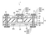
図10に示すように、実施形態の電子部品内蔵基板1では、厚み方向の中央部にコア材12が配置されており、コア材12はその厚み方向に貫通する開口部12aを備えている。コア材12の開口部12aにチップキャパシタ20が配置されている。チップキャパシタ20は横方向の両端側に接続端子22を備えている。コア材12の厚みはチップキャパシタ20の全体の厚みに対応している。
As shown in FIG. 10, in the electronic component built-in
コア材12の下面(一方の面)には、第1内側補助絶縁層30aが形成されており、コア材12の開口部12aの側面とチップキャパシタ20との隙間が充填樹脂部30cで埋め込まれている。第1内側補助絶縁層30aの下には第1外側補助絶縁層30bが積層されており、第1内側補助絶縁層30a及び第1外側補助絶縁層30bによって第1補助絶縁層30が形成される。
A first inner auxiliary insulating
このように、コア材12の下面側の第1補助絶縁層30は、複数の樹脂層が積層されて形成され、コア材12に接触する第1内側補助絶縁層30aがコア材12の開口部12aに充填されて、充填樹脂部30cが形成される。また、コア材12の上面(他方の面)には第2補助絶縁層32が形成されている。
Thus, the first auxiliary insulating
コア材12は、その一方の面及び他方の面の全体にわたって第1補助絶縁層30及び第2補助絶縁層32と直接接触しており、それらの界面に配線層は介在していない。これにより、コア材12、第1補助絶縁層30及び第2補助絶縁層32によってコア基板10が形成されている。
The
コア材12の上面側において、第2補助絶縁層32にはチップキャパシタ20の接続端子22に到達する第1ビアホールVH1が形成されている。第2補助絶縁層32の上には、第1ビアホールVH1を介してチップキャパシタ20の接続端子22に接続される第1配線層40が形成されている。さらに、コア材12の下面側の第1補助絶縁層30の上に第1配線層40が形成されている。
On the upper surface side of the
また、コア材12の上面側において、第2補助絶縁層32及び第1配線層40の上に第1層間絶縁層50が形成されており、第1層間絶縁層50の中央部には第1配線層40に到達する第2ビアホールVH2が形成されている。上面側の第1層間絶縁層50の上には第2ビアホールVH2を介して第1配線層40に接続される第2配線層42が形成されている。
Further, on the upper surface side of the
コア材12の上面側の第1配線層40は、第2ビアホールVH2を形成する工程で高出力のレーザ加工を行う際のストッパ層として機能し、チップキャパシタ20の接続端子22がそのレーザ加工から保護される。このため、第1配線層40の厚みはチップキャパシタ20の接続端子22の厚みより厚く設定される。
The
コア材12の両面側の第1層間絶縁層50は、銅箔付プリプレグCPを熱プレスすることによりそれぞれ形成される。このため、第2配線層42は銅箔50b(金属箔)を含み、銅箔50bの上に第1金属めっき層42a及び第2金属めっき層42bが積層されて形成される。
The first
また、コア材12の下面側において、第1補助絶縁層30及び第1配線層40の上に第1層間絶縁層50が形成されている。
A first
さらに、電子部品内蔵基板1の両端部には、上面側の第1層間絶縁層50から下面側の第1層間絶縁層50まで貫通して形成されたスルーホールTHが設けられている。両面側の第1層間絶縁層50上において、スルーホールTHの上に配置された第2配線層42は、スルーホールTHの側面に延在する第1金属めっき層42aを介して相互接続されている。また、両面側の第2配線層42は、スルーホールTHの側面の第1金属めっき層42aを介して第1配線層40に接続されている。
Further, through holes TH formed so as to penetrate from the first
前述したように、本実施形態の電子部品内蔵基板の製造方法では、コア材12の厚みをチップキャパシタ20の厚みに対応させている。これにより、コア材12の開口部12aに配置されたチップキャパシタ20の周りの隙間を、樹脂フィルム30xを熱プレスして埋め込む際に、埋め込む空間の体積を小さくすることができる。
As described above, in the manufacturing method of the electronic component built-in substrate according to the present embodiment, the thickness of the
これにより、樹脂フィルム30xを低い押圧力で熱プレスすることによって、チップキャパシタ20の周辺を隙間なく樹脂で信頼性よく埋め込むことができる。従って、チップキャパシタ20にかかる圧力も小さくなるため、チップキャパシタ20が仮付フィルム18から剥がれて傾くことが防止される。
Thereby, the periphery of the
そして、コア材12の厚みの不足分を第1補助絶縁層30及び第2補助絶縁層32によって補って調整することにより、所望の厚みのコア基板10を得ることができる。これによって、伝送経路のインピーダンス整合などの設計スペックを満足させることができる。
Then, the
また、チップキャパシタ20の接続端子22は、第2補助絶縁層32の第2ビアホールVH2を介して厚みの厚い第1配線層40によってかさ上げされている。そして、第1配線層40の上に銅箔付プリプレグCPが積層されて、銅箔50bが接着された第1層間絶縁層50が形成される。
The
このため、銅箔50b及びプリプレグ50aから形成される第1層間絶縁層50を高出力のレーザで加工して第2ビアホールVH2を形成する際に、厚みの厚い第1配線層40がレーザ加工にストッパ層として機能する。
Therefore, when the first
これにより、チップキャパシタ20の接続端子22は第1配線層40によって保護されるため、レーザ加工で損傷が生じるおそれがない。このため、チップキャパシタ20の接続端子22は、第1、第2配線層40,42と信頼性よく電気的に接続される。
Thereby, since the
以上のように、本実施形態では、設計スペックの所望の特性を有する電子部品内蔵基板を歩留りよく製造できると共に、電子部品内蔵基板の信頼性を向上させることができる。 As described above, according to the present embodiment, an electronic component built-in substrate having desired characteristics of design specifications can be manufactured with high yield, and the reliability of the electronic component built-in substrate can be improved.
図11には、最上の配線層に半導体チップが接続される場合に好適に使用される電子部品内蔵基板2が示されている。図11の電子部品内蔵基板2では、図10の電子部品内蔵基板1の両面側に第2層間絶縁層52がそれぞれ形成されている。
FIG. 11 shows the electronic component built-in
第2層間絶縁層52はエポキシ樹脂やポリイミド樹脂などの樹脂フィルムが積層されて形成される。両面側の第2層間絶縁層52には、第2配線層42に到達する第3ビアホールVH3が形成されている。第3ビアホールVH3は、第2層間絶縁層52がレーザによって加工されて形成される。
The second
さらに、コア材12の両面側の第2層間絶縁層52の上に、第3ビアホールVH3を介して第2配線層42に接続される第3配線層44がそれぞれ形成されている。第3配線層44はセミアディティブ法などで形成される。
Further, third wiring layers 44 connected to the
また、コア材12の両面側の第2層間絶縁層52の上に、第3配線層44のパッド部上に開口部54aが設けられたソルダレジスト54がそれぞれ形成されている。必要に応じて、両面側の第3配線層44のパッド部にニッケル/金めっき層などのコンタクト層(不図示)が形成される。配線層の積層数は任意に設定することができる。
Further, solder resists 54 each having an opening 54 a on the pad portion of the
そして、図12に示すように、図11の電子部品内蔵基板2の上面側の第3配線層44のパッド部に半導体チップ60のバンプ電極62がフリップチップ接続される。さらに、半導体チップ60の下側の隙間にアンダーフィル樹脂64が充填される。
Then, as shown in FIG. 12, the
1,2…電子部品内蔵基板、10…コア基板、12…コア材、12a,54a…開口部、14,50b…銅箔、16…銅張積層板、18…仮付テープ、20…チップキャパシタ、22…接続端子、30…第1補助絶縁層、30a…第1内側補助絶縁層、30b…第1外側補助絶縁層、30c…充填樹脂部、30x…樹脂フィルム、32…第2補助絶縁層、40…第1配線層、42…第2配線層、42a…第1金属めっき層、42b…第2金属めっき層、44…第3配線層、50…第1層間絶縁層、50a…プリプレグ、52…第2層間絶縁層、54…ソルダレジスト、60…半導体チップ、62…バンプ電極、64…アンダーフィル樹脂、CP…銅箔付プリプレグ、VH1…第1ビアホール、VH2…第2ビアホール、VH3…第3ビアホール、R…樹脂体、TH…スルーホール。
DESCRIPTION OF
Claims (8)
前記開口部内に電子部品を搭載する工程と、
前記コア材の一方の面に第1樹脂層を形成すると共に、前記コア材の開口部の側面と前記電子部品との隙間に前記第1樹脂層を充填して充填樹脂部を形成する工程と、
前記コア材の他方の面に第2補助絶縁層を形成する共に、前記コア材の一方の面の前記第1樹脂層の上に第2樹脂層を積層して、前記第1樹脂層と前記第2樹脂層とからなる第1補助絶縁層を形成する工程と、
前記第2補助絶縁層に、前記電子部品の接続端子に到達する第1ビアホールを形成する工程と、
前記第2補助絶縁層の上に、前記第1ビアホールを介して前記電子部品の接続端子に接続される第1配線層を形成する工程とを有し、
前記コア材は前記一方の面及び他方の面の全体にわたって前記第1補助絶縁層及び前記第2補助絶縁層と直接接触しており、前記コア材、前記第1補助絶縁層及び前記第2補助絶縁層により基板が形成されることを特徴とする電子部品内蔵基板の製造方法。 Forming an opening in the core material;
Mounting an electronic component in the opening;
Forming a first resin layer on one surface of the core material, and filling the first resin layer in a gap between the side surface of the opening of the core material and the electronic component to form a filled resin portion; ,
A second auxiliary insulating layer is formed on the other surface of the core material, and a second resin layer is laminated on the first resin layer on the one surface of the core material, and the first resin layer and the Forming a first auxiliary insulating layer comprising a second resin layer;
Forming a first via hole reaching the connection terminal of the electronic component in the second auxiliary insulating layer;
Forming a first wiring layer connected to the connection terminal of the electronic component through the first via hole on the second auxiliary insulating layer;
The core material is in direct contact with the first auxiliary insulating layer and the second auxiliary insulating layer over the entire one surface and the other surface, and the core material, the first auxiliary insulating layer, and the second auxiliary material are in contact with each other. A method of manufacturing a substrate with built-in electronic components, wherein the substrate is formed of an insulating layer.
前記コア材の他方の面に仮付テープを貼り付ける工程と、
前記コア材の開口部内の前記仮付テープに前記電子部品を搭載する工程とを含み、
前記充填樹脂部を充填する工程の後に、前記仮付テープを除去する工程を有することを特徴とする請求項1又は2に記載の電子部品内蔵基板の製造方法。 The step of mounting the electronic component includes:
A step of attaching a temporary tape to the other surface of the core material;
Mounting the electronic component on the temporary tape in the opening of the core material,
3. The method of manufacturing an electronic component built-in substrate according to claim 1, further comprising a step of removing the temporary tape after the step of filling the filling resin portion.
前記第2補助絶縁層の上に層間絶縁層を形成する工程と、
前記層間絶縁層に、前記第1配線層に到達する第2ビアホールを形成する工程と、
前記層間絶縁層の上に、前記第2ビアホールを介して前記第1配線層に接続される第2配線層を形成する工程とを有することを特徴とする請求項1乃至3のいずれか一項に記載の電子部品内蔵基板の製造方法。 After the step of forming the first wiring layer,
Forming an interlayer insulating layer on the second auxiliary insulating layer;
Forming a second via hole reaching the first wiring layer in the interlayer insulating layer;
4. A step of forming a second wiring layer connected to the first wiring layer through the second via hole on the interlayer insulating layer. 5. The manufacturing method of the electronic component built-in board as described in 2.
前記第2ビアホールを形成する工程において、前記銅箔及び前記層間絶縁層をレーザで加工し、
前記第2配線層を形成する工程において、前記第2配線層は前記銅箔を含んで形成されることを特徴とする請求項4に記載の電子部品内蔵基板の製造方法。 In the step of forming the interlayer insulating layer, the interlayer insulating layer is formed by hot pressing a prepreg with a copper foil, and the copper foil is bonded on the interlayer insulating layer,
In the step of forming the second via hole, the copper foil and the interlayer insulating layer are processed with a laser,
5. The method of manufacturing an electronic component built-in substrate according to claim 4, wherein in the step of forming the second wiring layer, the second wiring layer is formed including the copper foil.
Priority Applications (3)
| Application Number | Priority Date | Filing Date | Title |
|---|---|---|---|
| JP2012122588A JP6009228B2 (en) | 2012-05-30 | 2012-05-30 | Manufacturing method of electronic component built-in substrate |
| KR1020130060110A KR102032171B1 (en) | 2012-05-30 | 2013-05-28 | Electronic component built-in substrate and method of manufacturing the same |
| US13/904,447 US9247646B2 (en) | 2012-05-30 | 2013-05-29 | Electronic component built-in substrate and method of manufacturing the same |
Applications Claiming Priority (1)
| Application Number | Priority Date | Filing Date | Title |
|---|---|---|---|
| JP2012122588A JP6009228B2 (en) | 2012-05-30 | 2012-05-30 | Manufacturing method of electronic component built-in substrate |
Publications (3)
| Publication Number | Publication Date |
|---|---|
| JP2013247353A JP2013247353A (en) | 2013-12-09 |
| JP2013247353A5 JP2013247353A5 (en) | 2015-07-02 |
| JP6009228B2 true JP6009228B2 (en) | 2016-10-19 |
Family
ID=49668866
Family Applications (1)
| Application Number | Title | Priority Date | Filing Date |
|---|---|---|---|
| JP2012122588A Active JP6009228B2 (en) | 2012-05-30 | 2012-05-30 | Manufacturing method of electronic component built-in substrate |
Country Status (3)
| Country | Link |
|---|---|
| US (1) | US9247646B2 (en) |
| JP (1) | JP6009228B2 (en) |
| KR (1) | KR102032171B1 (en) |
Families Citing this family (14)
| Publication number | Priority date | Publication date | Assignee | Title |
|---|---|---|---|---|
| US9711392B2 (en) * | 2012-07-25 | 2017-07-18 | Infineon Technologies Ag | Field emission devices and methods of making thereof |
| TWI610606B (en) * | 2013-02-21 | 2018-01-01 | 味之素股份有限公司 | Manufacturing method and semiconductor device for built-in wiring board of parts |
| JP2015035497A (en) * | 2013-08-09 | 2015-02-19 | イビデン株式会社 | Electronic component built-in wiring board |
| JP6350093B2 (en) * | 2013-12-16 | 2018-07-04 | 味の素株式会社 | Method for manufacturing component-embedded substrate and semiconductor device |
| KR102281468B1 (en) | 2014-07-16 | 2021-07-27 | 삼성전기주식회사 | Chip embedded substrate and method of manufacturing the same |
| US9420693B2 (en) * | 2014-09-18 | 2016-08-16 | Intel Corporation | Integration of embedded thin film capacitors in package substrates |
| JP6428164B2 (en) * | 2014-10-31 | 2018-11-28 | 日立化成株式会社 | Semiconductor device and manufacturing method thereof |
| KR102356810B1 (en) * | 2015-01-22 | 2022-01-28 | 삼성전기주식회사 | Printed circuit board having embedded electronic devices and method of manufacturing the same |
| JP6712764B2 (en) | 2015-05-25 | 2020-06-24 | パナソニックIpマネジメント株式会社 | Stretchable flexible substrate and manufacturing method thereof |
| JP6639934B2 (en) * | 2016-02-08 | 2020-02-05 | 新光電気工業株式会社 | Wiring board, semiconductor device, and method of manufacturing wiring board |
| US11270920B2 (en) * | 2018-08-14 | 2022-03-08 | Medtronic, Inc. | Integrated circuit package and method of forming same |
| US10903169B2 (en) * | 2019-04-30 | 2021-01-26 | Advanced Semiconductor Engineering, Inc. | Conductive structure and wiring structure including the same |
| CN112026329B (en) * | 2020-09-15 | 2021-05-11 | 福建鑫宏华机械有限公司 | Manufacturing method of aluminum-based copper-clad plate |
| KR20220130916A (en) * | 2021-03-19 | 2022-09-27 | 삼성전기주식회사 | Substrate with electronic component embedded therein |
Family Cites Families (5)
| Publication number | Priority date | Publication date | Assignee | Title |
|---|---|---|---|---|
| JP4551468B2 (en) * | 2007-09-05 | 2010-09-29 | 太陽誘電株式会社 | Electronic component built-in multilayer board |
| JP5284155B2 (en) * | 2008-03-24 | 2013-09-11 | 日本特殊陶業株式会社 | Component built-in wiring board |
| US8120158B2 (en) * | 2009-11-10 | 2012-02-21 | Infineon Technologies Ag | Laminate electronic device |
| KR101084252B1 (en) * | 2010-03-05 | 2011-11-17 | 삼성전기주식회사 | Electro device embedded printed circuit board and manufacturing method thereof |
| JP5001395B2 (en) | 2010-03-31 | 2012-08-15 | イビデン株式会社 | Wiring board and method of manufacturing wiring board |
-
2012
- 2012-05-30 JP JP2012122588A patent/JP6009228B2/en active Active
-
2013
- 2013-05-28 KR KR1020130060110A patent/KR102032171B1/en active IP Right Grant
- 2013-05-29 US US13/904,447 patent/US9247646B2/en active Active
Also Published As
| Publication number | Publication date |
|---|---|
| US9247646B2 (en) | 2016-01-26 |
| US20130319740A1 (en) | 2013-12-05 |
| KR102032171B1 (en) | 2019-10-16 |
| KR20130135097A (en) | 2013-12-10 |
| JP2013247353A (en) | 2013-12-09 |
Similar Documents
| Publication | Publication Date | Title |
|---|---|---|
| JP6009228B2 (en) | Manufacturing method of electronic component built-in substrate | |
| JP6200178B2 (en) | Electronic component built-in substrate and manufacturing method thereof | |
| JP4635033B2 (en) | Wiring board manufacturing method and electronic component mounting structure manufacturing method | |
| WO2006011320A1 (en) | Composite electronic component and its manufacturing method | |
| JP2008522397A (en) | Electronic module and manufacturing method thereof | |
| JP6208411B2 (en) | Wiring board and manufacturing method thereof | |
| JP2011199077A (en) | Method of manufacturing multilayer wiring board | |
| US10743422B2 (en) | Embedding a component in a core on conductive foil | |
| JP2017073458A (en) | Wiring board and manufacturing method therefor | |
| JP4460341B2 (en) | Wiring board and manufacturing method thereof | |
| JP4183708B2 (en) | Manufacturing method of component-embedded substrate | |
| JP2002076637A (en) | Substrate incorporating chip component, and manufacturing method of the substrate | |
| WO2012128269A1 (en) | Wiring substrate | |
| JP6669330B2 (en) | Printed circuit board with built-in electronic components and method of manufacturing the same | |
| JP2012064600A (en) | Multilayer substrate and method of manufacturing the same | |
| JP2008182039A (en) | Multilayer wiring board and its manufacturing method | |
| JP2017028024A (en) | Component mounted board, component built-in board, manufacturing method of component mounted board and manufacturing method of component built-in board | |
| JP5385699B2 (en) | Manufacturing method of multilayer wiring board | |
| JP2013183015A (en) | Electronic component containing multilayer wiring board and method for manufacturing the same | |
| KR101205464B1 (en) | Method for manufacturing a printed circuit board | |
| JP5432354B2 (en) | Temporary board for manufacturing wiring board and method for manufacturing the same | |
| KR101138542B1 (en) | Manufactory method for multi-layer printed circuit board | |
| JP5491991B2 (en) | Multilayer wiring board and manufacturing method thereof | |
| JP5097006B2 (en) | Printed wiring board and manufacturing method thereof | |
| KR100796981B1 (en) | Method for manufacturing printed circuit board |
Legal Events
| Date | Code | Title | Description |
|---|---|---|---|
| A521 | Written amendment |
Free format text: JAPANESE INTERMEDIATE CODE: A523 Effective date: 20150519 |
|
| A621 | Written request for application examination |
Free format text: JAPANESE INTERMEDIATE CODE: A621 Effective date: 20150519 |
|
| A977 | Report on retrieval |
Free format text: JAPANESE INTERMEDIATE CODE: A971007 Effective date: 20160209 |
|
| A131 | Notification of reasons for refusal |
Free format text: JAPANESE INTERMEDIATE CODE: A131 Effective date: 20160223 |
|
| A521 | Written amendment |
Free format text: JAPANESE INTERMEDIATE CODE: A523 Effective date: 20160401 |
|
| A02 | Decision of refusal |
Free format text: JAPANESE INTERMEDIATE CODE: A02 Effective date: 20160621 |
|
| A521 | Written amendment |
Free format text: JAPANESE INTERMEDIATE CODE: A523 Effective date: 20160727 |
|
| A911 | Transfer to examiner for re-examination before appeal (zenchi) |
Free format text: JAPANESE INTERMEDIATE CODE: A911 Effective date: 20160804 |
|
| TRDD | Decision of grant or rejection written | ||
| A01 | Written decision to grant a patent or to grant a registration (utility model) |
Free format text: JAPANESE INTERMEDIATE CODE: A01 Effective date: 20160906 |
|
| A61 | First payment of annual fees (during grant procedure) |
Free format text: JAPANESE INTERMEDIATE CODE: A61 Effective date: 20160914 |
|
| R150 | Certificate of patent or registration of utility model |
Ref document number: 6009228 Country of ref document: JP Free format text: JAPANESE INTERMEDIATE CODE: R150 |