WO2012128269A1 - Wiring substrate - Google Patents
Wiring substrate Download PDFInfo
- Publication number
- WO2012128269A1 WO2012128269A1 PCT/JP2012/057120 JP2012057120W WO2012128269A1 WO 2012128269 A1 WO2012128269 A1 WO 2012128269A1 JP 2012057120 W JP2012057120 W JP 2012057120W WO 2012128269 A1 WO2012128269 A1 WO 2012128269A1
- Authority
- WO
- WIPO (PCT)
- Prior art keywords
- interlayer connection
- connection conductor
- insulating layer
- wiring board
- conductive pattern
- Prior art date
Links
Images


Classifications
-
- H—ELECTRICITY
- H05—ELECTRIC TECHNIQUES NOT OTHERWISE PROVIDED FOR
- H05K—PRINTED CIRCUITS; CASINGS OR CONSTRUCTIONAL DETAILS OF ELECTRIC APPARATUS; MANUFACTURE OF ASSEMBLAGES OF ELECTRICAL COMPONENTS
- H05K1/00—Printed circuits
- H05K1/18—Printed circuits structurally associated with non-printed electric components
- H05K1/182—Printed circuits structurally associated with non-printed electric components associated with components mounted in the printed circuit board, e.g. insert mounted components [IMC]
- H05K1/185—Components encapsulated in the insulating substrate of the printed circuit or incorporated in internal layers of a multilayer circuit
- H05K1/188—Components encapsulated in the insulating substrate of the printed circuit or incorporated in internal layers of a multilayer circuit manufactured by mounting on or attaching to a structure having a conductive layer, e.g. a metal foil, such that the terminals of the component are connected to or adjacent to the conductive layer before embedding, and by using the conductive layer, which is patterned after embedding, at least partially for connecting the component
-
- H—ELECTRICITY
- H05—ELECTRIC TECHNIQUES NOT OTHERWISE PROVIDED FOR
- H05K—PRINTED CIRCUITS; CASINGS OR CONSTRUCTIONAL DETAILS OF ELECTRIC APPARATUS; MANUFACTURE OF ASSEMBLAGES OF ELECTRICAL COMPONENTS
- H05K1/00—Printed circuits
- H05K1/02—Details
- H05K1/0296—Conductive pattern lay-out details not covered by sub groups H05K1/02 - H05K1/0295
- H05K1/0298—Multilayer circuits
-
- H—ELECTRICITY
- H01—ELECTRIC ELEMENTS
- H01L—SEMICONDUCTOR DEVICES NOT COVERED BY CLASS H10
- H01L23/00—Details of semiconductor or other solid state devices
- H01L23/52—Arrangements for conducting electric current within the device in operation from one component to another, i.e. interconnections, e.g. wires, lead frames
- H01L23/538—Arrangements for conducting electric current within the device in operation from one component to another, i.e. interconnections, e.g. wires, lead frames the interconnection structure between a plurality of semiconductor chips being formed on, or in, insulating substrates
- H01L23/5389—Arrangements for conducting electric current within the device in operation from one component to another, i.e. interconnections, e.g. wires, lead frames the interconnection structure between a plurality of semiconductor chips being formed on, or in, insulating substrates the chips being integrally enclosed by the interconnect and support structures
-
- H—ELECTRICITY
- H01—ELECTRIC ELEMENTS
- H01L—SEMICONDUCTOR DEVICES NOT COVERED BY CLASS H10
- H01L24/00—Arrangements for connecting or disconnecting semiconductor or solid-state bodies; Methods or apparatus related thereto
- H01L24/01—Means for bonding being attached to, or being formed on, the surface to be connected, e.g. chip-to-package, die-attach, "first-level" interconnects; Manufacturing methods related thereto
- H01L24/18—High density interconnect [HDI] connectors; Manufacturing methods related thereto
-
- H—ELECTRICITY
- H05—ELECTRIC TECHNIQUES NOT OTHERWISE PROVIDED FOR
- H05K—PRINTED CIRCUITS; CASINGS OR CONSTRUCTIONAL DETAILS OF ELECTRIC APPARATUS; MANUFACTURE OF ASSEMBLAGES OF ELECTRICAL COMPONENTS
- H05K1/00—Printed circuits
- H05K1/02—Details
- H05K1/03—Use of materials for the substrate
- H05K1/0313—Organic insulating material
-
- H—ELECTRICITY
- H05—ELECTRIC TECHNIQUES NOT OTHERWISE PROVIDED FOR
- H05K—PRINTED CIRCUITS; CASINGS OR CONSTRUCTIONAL DETAILS OF ELECTRIC APPARATUS; MANUFACTURE OF ASSEMBLAGES OF ELECTRICAL COMPONENTS
- H05K1/00—Printed circuits
- H05K1/02—Details
- H05K1/09—Use of materials for the conductive, e.g. metallic pattern
-
- H—ELECTRICITY
- H05—ELECTRIC TECHNIQUES NOT OTHERWISE PROVIDED FOR
- H05K—PRINTED CIRCUITS; CASINGS OR CONSTRUCTIONAL DETAILS OF ELECTRIC APPARATUS; MANUFACTURE OF ASSEMBLAGES OF ELECTRICAL COMPONENTS
- H05K1/00—Printed circuits
- H05K1/18—Printed circuits structurally associated with non-printed electric components
- H05K1/181—Printed circuits structurally associated with non-printed electric components associated with surface mounted components
-
- H—ELECTRICITY
- H05—ELECTRIC TECHNIQUES NOT OTHERWISE PROVIDED FOR
- H05K—PRINTED CIRCUITS; CASINGS OR CONSTRUCTIONAL DETAILS OF ELECTRIC APPARATUS; MANUFACTURE OF ASSEMBLAGES OF ELECTRICAL COMPONENTS
- H05K3/00—Apparatus or processes for manufacturing printed circuits
- H05K3/40—Forming printed elements for providing electric connections to or between printed circuits
- H05K3/4038—Through-connections; Vertical interconnect access [VIA] connections
-
- H—ELECTRICITY
- H05—ELECTRIC TECHNIQUES NOT OTHERWISE PROVIDED FOR
- H05K—PRINTED CIRCUITS; CASINGS OR CONSTRUCTIONAL DETAILS OF ELECTRIC APPARATUS; MANUFACTURE OF ASSEMBLAGES OF ELECTRICAL COMPONENTS
- H05K3/00—Apparatus or processes for manufacturing printed circuits
- H05K3/46—Manufacturing multilayer circuits
- H05K3/4644—Manufacturing multilayer circuits by building the multilayer layer by layer, i.e. build-up multilayer circuits
- H05K3/4647—Manufacturing multilayer circuits by building the multilayer layer by layer, i.e. build-up multilayer circuits by applying an insulating layer around previously made via studs
-
- H—ELECTRICITY
- H01—ELECTRIC ELEMENTS
- H01L—SEMICONDUCTOR DEVICES NOT COVERED BY CLASS H10
- H01L23/00—Details of semiconductor or other solid state devices
- H01L23/48—Arrangements for conducting electric current to or from the solid state body in operation, e.g. leads, terminal arrangements ; Selection of materials therefor
- H01L23/488—Arrangements for conducting electric current to or from the solid state body in operation, e.g. leads, terminal arrangements ; Selection of materials therefor consisting of soldered or bonded constructions
- H01L23/498—Leads, i.e. metallisations or lead-frames on insulating substrates, e.g. chip carriers
- H01L23/49822—Multilayer substrates
-
- H—ELECTRICITY
- H01—ELECTRIC ELEMENTS
- H01L—SEMICONDUCTOR DEVICES NOT COVERED BY CLASS H10
- H01L23/00—Details of semiconductor or other solid state devices
- H01L23/48—Arrangements for conducting electric current to or from the solid state body in operation, e.g. leads, terminal arrangements ; Selection of materials therefor
- H01L23/488—Arrangements for conducting electric current to or from the solid state body in operation, e.g. leads, terminal arrangements ; Selection of materials therefor consisting of soldered or bonded constructions
- H01L23/498—Leads, i.e. metallisations or lead-frames on insulating substrates, e.g. chip carriers
- H01L23/49827—Via connections through the substrates, e.g. pins going through the substrate, coaxial cables
-
- H—ELECTRICITY
- H01—ELECTRIC ELEMENTS
- H01L—SEMICONDUCTOR DEVICES NOT COVERED BY CLASS H10
- H01L23/00—Details of semiconductor or other solid state devices
- H01L23/48—Arrangements for conducting electric current to or from the solid state body in operation, e.g. leads, terminal arrangements ; Selection of materials therefor
- H01L23/488—Arrangements for conducting electric current to or from the solid state body in operation, e.g. leads, terminal arrangements ; Selection of materials therefor consisting of soldered or bonded constructions
- H01L23/498—Leads, i.e. metallisations or lead-frames on insulating substrates, e.g. chip carriers
- H01L23/49838—Geometry or layout
-
- H—ELECTRICITY
- H01—ELECTRIC ELEMENTS
- H01L—SEMICONDUCTOR DEVICES NOT COVERED BY CLASS H10
- H01L23/00—Details of semiconductor or other solid state devices
- H01L23/52—Arrangements for conducting electric current within the device in operation from one component to another, i.e. interconnections, e.g. wires, lead frames
- H01L23/538—Arrangements for conducting electric current within the device in operation from one component to another, i.e. interconnections, e.g. wires, lead frames the interconnection structure between a plurality of semiconductor chips being formed on, or in, insulating substrates
- H01L23/5383—Multilayer substrates
-
- H—ELECTRICITY
- H01—ELECTRIC ELEMENTS
- H01L—SEMICONDUCTOR DEVICES NOT COVERED BY CLASS H10
- H01L23/00—Details of semiconductor or other solid state devices
- H01L23/52—Arrangements for conducting electric current within the device in operation from one component to another, i.e. interconnections, e.g. wires, lead frames
- H01L23/538—Arrangements for conducting electric current within the device in operation from one component to another, i.e. interconnections, e.g. wires, lead frames the interconnection structure between a plurality of semiconductor chips being formed on, or in, insulating substrates
- H01L23/5384—Conductive vias through the substrate with or without pins, e.g. buried coaxial conductors
-
- H—ELECTRICITY
- H01—ELECTRIC ELEMENTS
- H01L—SEMICONDUCTOR DEVICES NOT COVERED BY CLASS H10
- H01L23/00—Details of semiconductor or other solid state devices
- H01L23/52—Arrangements for conducting electric current within the device in operation from one component to another, i.e. interconnections, e.g. wires, lead frames
- H01L23/538—Arrangements for conducting electric current within the device in operation from one component to another, i.e. interconnections, e.g. wires, lead frames the interconnection structure between a plurality of semiconductor chips being formed on, or in, insulating substrates
- H01L23/5386—Geometry or layout of the interconnection structure
-
- H—ELECTRICITY
- H05—ELECTRIC TECHNIQUES NOT OTHERWISE PROVIDED FOR
- H05K—PRINTED CIRCUITS; CASINGS OR CONSTRUCTIONAL DETAILS OF ELECTRIC APPARATUS; MANUFACTURE OF ASSEMBLAGES OF ELECTRICAL COMPONENTS
- H05K2201/00—Indexing scheme relating to printed circuits covered by H05K1/00
- H05K2201/03—Conductive materials
- H05K2201/0332—Structure of the conductor
- H05K2201/0364—Conductor shape
- H05K2201/0367—Metallic bump or raised conductor not used as solder bump
-
- H—ELECTRICITY
- H05—ELECTRIC TECHNIQUES NOT OTHERWISE PROVIDED FOR
- H05K—PRINTED CIRCUITS; CASINGS OR CONSTRUCTIONAL DETAILS OF ELECTRIC APPARATUS; MANUFACTURE OF ASSEMBLAGES OF ELECTRICAL COMPONENTS
- H05K2201/00—Indexing scheme relating to printed circuits covered by H05K1/00
- H05K2201/10—Details of components or other objects attached to or integrated in a printed circuit board
- H05K2201/10613—Details of electrical connections of non-printed components, e.g. special leads
- H05K2201/10621—Components characterised by their electrical contacts
- H05K2201/10674—Flip chip
-
- H—ELECTRICITY
- H05—ELECTRIC TECHNIQUES NOT OTHERWISE PROVIDED FOR
- H05K—PRINTED CIRCUITS; CASINGS OR CONSTRUCTIONAL DETAILS OF ELECTRIC APPARATUS; MANUFACTURE OF ASSEMBLAGES OF ELECTRICAL COMPONENTS
- H05K2203/00—Indexing scheme relating to apparatus or processes for manufacturing printed circuits covered by H05K3/00
- H05K2203/03—Metal processing
- H05K2203/0323—Working metal substrate or core, e.g. by etching, deforming
-
- H—ELECTRICITY
- H05—ELECTRIC TECHNIQUES NOT OTHERWISE PROVIDED FOR
- H05K—PRINTED CIRCUITS; CASINGS OR CONSTRUCTIONAL DETAILS OF ELECTRIC APPARATUS; MANUFACTURE OF ASSEMBLAGES OF ELECTRICAL COMPONENTS
- H05K2203/00—Indexing scheme relating to apparatus or processes for manufacturing printed circuits covered by H05K3/00
- H05K2203/14—Related to the order of processing steps
- H05K2203/1476—Same or similar kind of process performed in phases, e.g. coarse patterning followed by fine patterning
-
- H—ELECTRICITY
- H05—ELECTRIC TECHNIQUES NOT OTHERWISE PROVIDED FOR
- H05K—PRINTED CIRCUITS; CASINGS OR CONSTRUCTIONAL DETAILS OF ELECTRIC APPARATUS; MANUFACTURE OF ASSEMBLAGES OF ELECTRICAL COMPONENTS
- H05K3/00—Apparatus or processes for manufacturing printed circuits
- H05K3/40—Forming printed elements for providing electric connections to or between printed circuits
- H05K3/4007—Surface contacts, e.g. bumps
Definitions
- the present invention relates to a wiring board having a conductor pattern formed on an insulating layer.
- an interlayer connection conductor (via hole conductor) that electrically connects wiring patterns between different layers is generally formed by providing a through hole in the wiring board and plating the inner wall of the through hole.
- the This forming method has a problem in productivity, economy, and the like because chemicals for plating are expensive or processing time is long.
- an interlayer connection conductor by filling a through-hole formed in an insulating layer of a wiring board with a conductive paste containing metal powder.
- the interlayer connection conductor is formed by filling a through hole with a conductive paste, and then densified by pressing a wiring circuit layer made of a metal foil.
- the conductive paste in the interlayer connection conductor oozes into the gap between the insulating layer and the wiring circuit layer, and the adhesion between the wiring circuit layer and the insulating layer is impaired. There is a risk of poor conduction in the substrate.
- Patent Document 1 discloses a wiring board that prevents the conductive paste in the interlayer connection conductor from leaching out to the periphery of the interlayer connection conductor and prevents poor adhesion between the wiring circuit layer and the insulating layer.
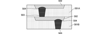
- FIG. 1 is a schematic cross-sectional view of a wiring board described in Patent Document 1.
- insulating layers 501A and 501B containing a thermosetting resin are laminated, and a wiring circuit layer 502 is buried on the surface thereof.
- the insulating layers 501A and 501B are provided with through holes for connecting the wiring circuit layers 502, and provided with interlayer connection conductors 503 in which the through holes are filled with a conductor component containing metal powder.
- the wiring circuit layer 502 is provided with a recess 504 in which the interlayer connection conductor 503 is buried. This recess 504 prevents the conductor paste of the interlayer connection conductor 503 from leaching out around the interlayer connection conductor 503.
- Patent Document 1 if the depth of the recess 504 formed in the wiring circuit layer 502 is too shallow, the effect of preventing the conductive paste from seeping out is small. If the depth is too deep, the wiring circuit layer 502 becomes thin and the wiring circuit layer 502 becomes thin. The strength of 502 may be reduced. Therefore, in patent document 1, since the adhesion defect of a wiring circuit layer and an insulating layer cannot fully be prevented, there exists a possibility that the connection reliability in a wiring board may fall.
- the conductor paste is filled in the through holes to form the interlayer connection conductor.
- the conductor paste is a resin containing metal powder
- the metal component in the interlayer connection conductor is reduced.
- the resistance value of the interlayer connection conductor is increased.
- the interlayer connection conductor hinders the current, and there is a problem that the wiring board cannot cope with a large current.
- an object of the present invention is to provide a wiring board capable of handling a large current without deteriorating connection reliability due to cracks, disconnection, delamination and the like.
- the wiring board according to the present invention includes an insulating layer, a first conductive pattern and a second conductive pattern disposed across the insulating layer, and the first conductive pattern and the first conductive layer penetrating the insulating layer in a thickness direction.
- An interlayer connection conductor that conducts two conductive patterns, and the interlayer connection conductor is integrally formed with the first conductive pattern, and the second is more than the junction interface between the insulating layer and the second conductive pattern.
- the second conductive pattern is joined to the second conductive pattern while being recessed into the conductive pattern side.
- the interlayer connection conductor that conducts the first conductive pattern and the second conductive pattern is formed integrally with the first conductive pattern, and the interlayer connection conductor is indented into the second conductive pattern side.
- the bonding interface between the interlayer connection conductor and the second conductive pattern is on a different plane from the bonding interface between the insulating layer and the second conductive pattern.
- integral formation means that a joining interface does not exist between an interlayer connection conductor and a 1st conductive pattern by being formed from one same metal member.
- the interlayer connection conductor is recessed into the second conductive pattern side, the junction interface between the interlayer connection conductor and the second conductive pattern and the junction interface between the insulating layer and the second conductive pattern are positioned on different planes.
- the generated stress can be dispersed, and conduction failure due to peeling, cracks generated in the wiring board, and the like can be prevented.
- the conductor pattern and the interlayer connection conductor are formed of different materials.
- the resistance value at the part increases.
- the resistance value of the connection portion between the first conductive pattern and the interlayer connection conductor may be increased. Therefore, such a problem can be avoided.
- the resistance value of the interlayer connection conductor can be reduced by increasing the metal component.
- the insulating layer may be composed of a plurality of layers, and may be formed on the surface of the uppermost layer of the insulating layer composed of a plurality of layers.
- the interlayer connection conductor and the second conductive pattern are electrically connected via a conductive adhesive.
- connection reliability between the interlayer connection conductor and the second conductive pattern can be improved by conducting through the conductive adhesive.
- an organic film is formed on at least a part of a bonding interface between the interlayer connection conductor and the second conductive pattern.
- At least the interlayer connection conductor is preferably subjected to a surface treatment.
- the surface treatment include roughening treatment, blackening treatment, coupling treatment, and organic film formation.
- the surface treatment site is essential for the surface of the interlayer connection conductor, together with the surface of the interlayer connection conductor, The first conductive pattern surface and the second conductive pattern surface may also be treated.
- the first conductive pattern includes a land integrally formed on the insulating layer side, and further includes an electronic component mounted on the land and disposed in the insulating layer. It may be configured.
- the wiring board can be reduced in size.
- the deepest portion of the interlayer connection conductor is embedded in the second conductive pattern by 10 ⁇ m or more.
- the expansion coefficient of the member is different because the bonding interface between the interlayer connection conductor and the second conductive pattern and the bonding interface between the second conductive pattern and the insulating layer are on different planes.
- the resulting stress can be dispersed.
- the resistance value of the interlayer connection conductor can be reduced by increasing the metal component.
- Schematic cross-sectional view of a wiring board according to Embodiment 3 The schematic diagram which showed the manufacturing process of the wiring board which concerns on Embodiment 3 in order.
- Schematic cross-sectional view of a wiring board according to Embodiment 4 The schematic diagram which showed the manufacturing process of the wiring board which concerns on Embodiment 4 in order.
- the wiring board according to the present invention includes an insulating layer made of an insulating resin and a conductive wiring pattern (conductive pattern) provided on the insulating layer.
- the insulating layer may be a single layer or a plurality of layers.
- the insulating resin forming the insulating layer include glass epoxy resin, epoxy resin, phenol resin, cyanate resin, and polyimide resin.
- a polyimide resin is preferable in that it has excellent heat resistance after curing.
- the wiring board electrically connects an electronic component mounted on the surface of the insulating layer and a main board (for example, a motherboard) on which the wiring board is mounted via a wiring pattern.
- the electronic component mounted on the wiring board is, for example, an active element such as a silicon semiconductor element or a gallium arsenide semiconductor element, or a passive element such as a capacitor or an inductor.
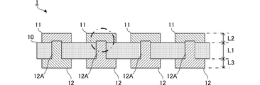
- FIG. 2 is a schematic cross-sectional view of the wiring board according to the first embodiment.
- FIG. 3 is an enlarged schematic diagram of the portion of the chain line circle in FIG. In FIG. 3, each component is actually in close contact, but for convenience of explanation, a space is provided at a joint portion of each component.
- the wiring substrate 1 according to Embodiment 1 has a configuration in which an upper wiring pattern 11 is formed on the upper surface of an insulating layer 10 and a lower wiring pattern 12 is formed on the lower surface.
- the upper surface of the insulating layer 10 is a surface on which the above-described electronic component is mounted.
- the insulating layer 10 has a thickness of 0.10 mm, and is formed with a cylindrical through via 10A.
- An interlayer connection conductor 12A formed integrally with a lower wiring pattern 12 described later is inserted through the through via 10A.
- the upper wiring pattern 11 and the lower wiring pattern 12 formed on the upper and lower surfaces of the insulating layer 10 are made conductive by the interlayer connection conductor 12A.
- the wiring pattern 11 is formed on the upper surface of the insulating layer 10 and has a thickness of 0.10 mm.
- the upper wiring pattern 11 has a distal end portion of a later-described interlayer connection conductor 12 ⁇ / b> A protruding from the insulating layer 10 at a position coinciding with the through via 10 ⁇ / b> A in the thickness direction formed in the insulating layer 10.
- the joint surface 11A of the upper wiring pattern 11 and the interlayer connection conductor 12A has an arcuate cross section as shown in FIG. 3, but may have a rectangular shape.
- the lower wiring pattern 12 is formed on the lower surface of the insulating layer 10 and has a thickness of 0.10 mm.
- the lower wiring pattern 12 is integrally formed with an interlayer connection conductor 12A. That is, the lower wiring pattern 12 and the interlayer connection conductor 12A are formed from the same metal member, and no bonding interface exists between them.
- the interlayer connection conductor 12A has a cylindrical shape with a diameter of 0.6 mm and a length of 0.2 mm, and the tip portion has an arc shape as shown in FIG.
- the interlayer connection conductor 12A is inserted through a through via 10A formed in the insulating layer 10.
- the tip of the interlayer connection conductor 12A protruding from the upper surface of the insulating layer 10 is buried in the upper wiring pattern 11 described above.
- the metal component increases in comparison with the case where the interlayer connection conductor is formed by filling the through hole with a conductive paste that is a resin containing metal powder. As a result, the resistance value of the interlayer connection conductor can be reduced.
- interlayer connection conductor 12A has a cylindrical shape, but may have a prismatic shape. Further, the tip of the interlayer connection conductor 12A may be planar.
- the bonding interface between the interlayer connection conductor 12A and the upper wiring pattern 11 is on a different plane from the bonding interface between the insulating layer 10 and the upper wiring pattern 11. Become.
- stress resulting from the difference in expansion coefficient can be prevented from concentrating on the bonding interface, and conduction failure due to peeling caused by the stress, cracks occurring in the wiring board 1, and the like can be prevented.
- FIG. 4 is a schematic diagram sequentially illustrating the manufacturing process of the wiring board 1 according to the first embodiment.
- a dry film resist 21 having a thickness of 15 ⁇ m is pasted on both sides facing each other in the thickness direction of the copper plate 20 having a thickness of 0.3 mm.
- FIG. 4 it is the figure seen from the side surface direction of the copper plate 20.
- a cylindrical interlayer connection conductor 12A having a diameter of 0.6 mm and a length of 0.2 mm on one side of the copper plate 20 to which the dry film resist 21 is attached. Etch so that remains.
- a 0.6 mm hole (not shown) is formed in the insulating resin 23 having a thickness of 0.15 mm, and is stacked on the copper plate 20 that has been etched in the second step. .
- This insulating resin 23 becomes the above-described insulating layer 10.
- a copper plate 24 having a thickness of 0.1 mm is placed on the upper surface of the insulating resin 23 (insulating layer 10), and in that state, laminated molding is performed at 180 ° C. and 100 kN for 1 hour. .
- laminated molding is performed at 180 ° C. and 100 kN for 1 hour. .
- the tip of the interlayer connection conductor 12A is recessed into the copper plate 24, and the above-described joining surface 11A is formed in an arc shape.
- the copper plate 20 is formed by patterning both surfaces of the laminate obtained in the fourth step by a subtractive method (a method of removing an unnecessary part and leaving a circuit).
- the lower wiring pattern 12 is formed, and the copper plate 24 is formed as the upper wiring pattern 11. Thereby, the wiring board 1 is formed.
- the amount by which the interlayer connection conductor 12A is buried in the upper wiring pattern 11 is preferably 50% or less of the thickness of the upper wiring pattern 11, but will be described below as more specific numerical values.
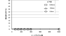
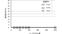
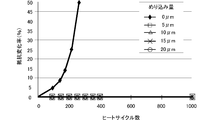
- FIG. 5 is a graph showing the results of a thermal shock test of the wiring board 1 according to the first embodiment.
- the vertical axis of the graph shown in FIG. 5 represents the resistance change rate (%) of the wiring board 1, and the horizontal axis represents the number of heat cycles in the thermal shock test.
- the depth of penetration is preferably 10 ⁇ m or more because the connection reliability decreases as the depth decreases.
- the amount of dent is 10 ⁇ m or more regardless of the diameter of the interlayer connection conductor 12 ⁇ / b> A and the thickness of the upper wiring pattern 11.
- FIG. 6 is a graph showing the relationship between the diameter of the interlayer connection conductor 12A and the connection reliability when the amount of penetration is 10 ⁇ m.
- FIG. 7 is a graph showing the relationship between the thickness of the upper wiring pattern 11 and the connection reliability when the depth of penetration is 10 ⁇ m.
- connection reliability is improved when the penetration amount is 10 ⁇ m or more is that the bonding interface between the upper wiring pattern 11 and the interlayer connection conductor 12A is the same as the bonding interface between the insulating layer 10 and the upper wiring pattern 11 having different thermal expansion coefficients. By not being on the plane. Therefore, this effect can be obtained regardless of the diameter of the interlayer connection conductor 12A and the thickness of the upper wiring pattern 11.
- the resistance change rate is not substantially changed regardless of the number of heat cycles.
- the resistance change rate is not substantially changed regardless of the number of heat cycles.
- the amount of indentation is 10 ⁇ m or more.
- the upper wiring pattern 11 has a thickness of 100 ⁇ m or more.
- FIG. 8 is a graph showing the relationship between the upper wiring pattern 11 and the amount of penetration.
- the vertical axis indicates the amount of indentation
- the horizontal axis indicates the thickness of the upper wiring pattern 11.
- the upper wiring pattern 11 has a thickness of about 100 ⁇ m, and when the thickness of the upper wiring pattern 11 is 100 ⁇ m or more, the amount of penetration is substantially constant. Therefore, if the upper wiring pattern 11 has a thickness of 100 ⁇ m or more, an optimal amount of penetration can be ensured of 10 ⁇ m or more.
- the wiring board 1 according to the second embodiment is different from the first embodiment in that the interlayer connection conductor 12A and the upper wiring pattern 11 are electrically connected via a conductive adhesive. Only the differences will be described below.
- FIG. 9 is a schematic cross-sectional view of the wiring board 1 according to the second embodiment.
- the wiring substrate 1 according to the second embodiment has a conductive adhesive 13 applied to the tip portion of the interlayer connection conductor 12 ⁇ / b> A.
- the conductive adhesive 13 is, for example, a low resistance conductive paste of nano silver or nano copper.
- the conductive adhesive 13 may be a resin composition containing metal powder.
- the conductive adhesive 13 is applied to the tip of the interlayer connection conductor 12A, the upper wiring pattern 11 and the interlayer connection conductor 12A are electrically connected via the conductive adhesive 13.
- the connection reliability of the interlayer connection conductor 12A can be further improved.
- the wiring board 1 which concerns on Embodiment 2, it is substantially the same as Embodiment 1, and apply
- the wiring board 1 according to the second embodiment can be manufactured.
- the amount of penetration is 10 ⁇ m or more.
- the amount of penetration can be 5 ⁇ m or more.
- FIG. 10 is a graph showing the results of a thermal shock test of the wiring board 1 according to the second embodiment. As shown in FIG. 10, when the amount of penetration is 5 ⁇ m or more, the resistance change rate is not substantially changed regardless of the number of heat cycles. Accordingly, the depth of penetration is preferably 5 ⁇ m or more because the connection reliability decreases with decreasing depth.
- the wiring board 1 according to the third embodiment is different from the first embodiment in that the insulating layer 10 is a multilayer and a wiring pattern is formed between the respective layers. Only the differences will be described below.
- FIG. 11 is a schematic cross-sectional view of the wiring board 1 according to the third embodiment.
- the insulating layer 10 of the wiring board 1 according to the third embodiment includes a first layer 101, a second layer 102, a third layer 103, and a fourth layer 104 sequentially from the surface side of the insulating layer 10. Has been configured.
- the upper wiring pattern 11 is formed on the upper surface of the first layer 101, and the lower wiring pattern 121 is formed on the lower surface.
- the lower wiring pattern 121 is integrally formed with an interlayer connection conductor 121A.
- the interlayer connection conductor 121A has a leading end protruding from the first layer 101 toward the upper wiring pattern 11 and a leading end recessed into the upper wiring pattern 11.
- the lower wiring pattern 122 is formed on the lower surface of the second layer 102.
- the lower wiring pattern 122 is integrally formed with an interlayer connection conductor 122A.
- the interlayer connection conductor 122 ⁇ / b> A protrudes from the second layer 102 to the lower wiring pattern 121 side and is recessed into the lower wiring pattern 121.
- the lower wiring pattern 123 is formed on the lower surface of the third layer 103.
- the lower wiring pattern 123 is integrally formed with an interlayer connection conductor 123A.
- the interlayer connection conductor 123 ⁇ / b> A protrudes from the third layer 103 to the lower wiring pattern 122 side and is recessed into the lower wiring pattern 122.
- the lower wiring pattern 124 is formed on the lower surface of the fourth layer 104.
- the lower wiring pattern 124 is integrally formed with an interlayer connection conductor 124A.
- the interlayer connection conductor 124 ⁇ / b> A protrudes from the fourth layer 104 to the lower wiring pattern 123 side and is recessed into the lower wiring pattern 123.
- the wiring board 1 according to the third embodiment has a multi-layered wiring pattern, and the wiring pattern of each layer has the tip of the interlayer connection conductor formed integrally with the lower wiring pattern embedded therein. .
- the wiring pattern of each layer has the tip of the interlayer connection conductor formed integrally with the lower wiring pattern embedded therein.
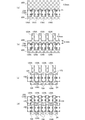
- FIG. 12 is a schematic diagram sequentially illustrating the manufacturing process of the wiring board 1 according to the third embodiment.
- the copper plate 204 is etched to form an interlayer connection conductor 124A, and the insulating resin 234 is laminated on the copper plate 204 so that the tip of the interlayer connection conductor 124A protrudes 0.05 mm.
- the insulating resin 234 becomes the fourth layer 104 in FIG.
- the copper plate 203 having a thickness of 0.3 mm is placed on the upper surface of the insulating resin 234 and laminated and molded at 180 ° C. and 100 kN for 1 hour. As a result, the tip end portion of the interlayer connection conductor 124 ⁇ / b> A comes into the copper plate 203.
- a dry film resist (not shown) having a thickness of 15 ⁇ m is attached to the upper surface of the copper plate 203, and the diameter is 0.6 mm and the length is 0.2 mm. Etching is performed so that the cylindrical interlayer connection conductor 123A remains.
- the copper plate 204 is formed as the lower wiring pattern 124 by patterning the both sides of the laminate obtained in FIG. 12B by the subtractive method.
- a copper plate 203 is formed as the lower wiring pattern 123.
- a 0.6 mm hole (not shown) is formed in the insulating resin 233 having a thickness of 0.15 mm, and the interlayer connection conductor formed in FIG.
- the insulating resin 233 is stacked so that 123A can be inserted.
- This insulating resin 233 becomes the third layer 103 in FIG.
- the wiring substrate 1 according to the third embodiment shown in FIG. 11 can be formed by sequentially repeating the steps described in FIG.
- the wiring board 1 can be further downsized by forming a wiring pattern in the inner layer of the insulating layer 10 and increasing the number of layers.
- the wiring board 1 according to the fourth embodiment is different from the third embodiment in that an electronic component is mounted in the insulating layer 10 of the wiring board 1 according to the third embodiment. Only the differences will be described below.
- FIG. 13 is a schematic cross-sectional view of the wiring board 1 according to the fourth embodiment.
- the first layer 101, the second layer 102, the third layer 103, and the fourth layer 104 are laminated in order from the surface side of the insulating layer 10. Has been configured.
- the lower wiring patterns 121, 122, 123, 124 formed on the lower surfaces of the first layer 101, the second layer 102, the third layer 103, and the fourth layer 104 are other than the interlayer connection conductors 121A, 122A, 123A, 124A.
- lands 121B, 122B, 123B, and 124B are integrally formed.
- Electronic parts 151, 152, 153, and 154 are mounted on the lands 121B, 122B, 123B, and 124B of each layer.
- the electronic components 151, 152, 153, and 154 are disposed in the first layer 101, the second layer 102, the third layer 103, and the fourth layer 104, respectively.
- the wiring board 1 can be reduced in size by incorporating the electronic components 151, 152, 153, and 154 in the insulating resin.
- the electronic components 151, 152, 153, and 154 include active elements such as silicon semiconductor elements and gallium arsenide semiconductor elements, or passive elements such as capacitors and inductors.
- FIG. 14 is a schematic diagram sequentially illustrating the manufacturing process of the wiring board 1 according to the fourth embodiment.
- a dry film resist (not shown) having a thickness of 15 ⁇ m is pasted on both sides facing each other in the thickness direction of the copper plate 20 having a thickness of 0.3 mm. Etching is performed so that a cylindrical interlayer connection conductor 124A having a diameter of 0.6 mm and a length of 0.19 mm remains on one surface of the copper plate 204 to which the dry film resist is attached.
- the copper plate 204 after the etching process in FIG. 14A is further etched to form a land 124B having a thickness of 0.01 mm.
- the interlayer connection conductor 124A formed with a length of 0.19 mm has a length of 0.2 mm.
- the electronic component 154 is mounted on the formed land 124B.
- the insulating resin 234 is laminated on the copper plate 204.
- the insulating resin 234 is in a liquid state, and after being applied onto the copper plate 204, vacuum-degassed and heated to seal the electronic component 154 in a semi-cured state. At this time, the insulating resin 234 has a thickness of 0.15 mm.
- a copper plate 203 having a thickness of 0.3 mm is placed, and laminate molding is performed at 180 ° C. and 100 kN for 1 hour. Thereafter, by repeating each process from the process of FIG. 14A, the wiring substrate 1 shown in FIG. 13 is formed.
- the wiring board 1 can be reduced in size by incorporating the electronic component in the insulating resin.
- the wiring board according to the present invention has been described in detail above. However, the specific configuration and the like of the wiring board 1 can be changed as appropriate, and the operations and effects described in the above-described embodiments are caused by the present invention. Only the most suitable actions and effects are listed, and the actions and effects according to the present invention are not limited to those described in the above embodiment.
Abstract
This wiring substrate is provided with an insulating layer (10) and an upper side wiring pattern (11) and lower side wiring pattern (12) disposed so as to sandwich the insulating layer (10). The lower side wiring pattern (12) protrudes into the upper side wiring pattern (11), and is formed integrally with an interlayer connecting conductor (12A) that is in electrical continuity with the upper side wiring pattern (11). The interlayer connecting conductor (12A) is joined to the upper layer wiring pattern (11) in a state of being sunk into the upper side wiring pattern (11) side above the joining interface for the insulating layer (10) and the upper side wiring pattern (11). Thus, connection reliability is not reduced by cracks, disconnections, interlayer peeling, and the like, and a wiring substrate that can handle large currents is provided.
Description
本発明は、絶縁層に導体パターンが形成された配線基板に関する。
The present invention relates to a wiring board having a conductor pattern formed on an insulating layer.
配線基板において、異なる層間の配線パターンを電気的に接続する層間接続導体(ビアホール導体)は、一般的には、配線基板に貫通孔を設けて、貫通孔の内壁にメッキを施すことで形成される。この形成方法は、メッキ処理にかかる化学薬品が高価なこと、又は、処理時間が長いことなどから生産性及び経済性等に問題がある。
In a wiring board, an interlayer connection conductor (via hole conductor) that electrically connects wiring patterns between different layers is generally formed by providing a through hole in the wiring board and plating the inner wall of the through hole. The This forming method has a problem in productivity, economy, and the like because chemicals for plating are expensive or processing time is long.
このため、例えば、配線基板の絶縁層に形成された貫通孔に金属粉末を含む導体ペーストを充填して層間接続導体を形成する方法がある。この方法では、層間接続導体は、貫通孔に導体ペーストを充填して形成された後、金属箔からなる配線回路層が押しつけられることによって緻密化される。このとき、配線回路層の押しつけにより、絶縁層と配線回路層との隙間に層間接続導体中の導体ペーストが浸み出し、配線回路層と絶縁層との密着性が損なわれ、その結果、配線基板における導通不良が生じるおそれがある。
For this reason, for example, there is a method of forming an interlayer connection conductor by filling a through-hole formed in an insulating layer of a wiring board with a conductive paste containing metal powder. In this method, the interlayer connection conductor is formed by filling a through hole with a conductive paste, and then densified by pressing a wiring circuit layer made of a metal foil. At this time, due to the pressing of the wiring circuit layer, the conductive paste in the interlayer connection conductor oozes into the gap between the insulating layer and the wiring circuit layer, and the adhesion between the wiring circuit layer and the insulating layer is impaired. There is a risk of poor conduction in the substrate.
特許文献1には、層間接続導体中の導体ペーストが層間接続導体周辺への浸み出すことを防止し、配線回路層と絶縁層との密着不良を防止する配線基板が開示されている。図1は特許文献1に記載の配線基板の模式的な断面図である。図1に示す配線基板は、熱硬化性樹脂を含む絶縁層501A,501Bが積層され、その表面に配線回路層502が埋没されている。
Patent Document 1 discloses a wiring board that prevents the conductive paste in the interlayer connection conductor from leaching out to the periphery of the interlayer connection conductor and prevents poor adhesion between the wiring circuit layer and the insulating layer. FIG. 1 is a schematic cross-sectional view of a wiring board described in Patent Document 1. In the wiring substrate shown in FIG. 1, insulating layers 501A and 501B containing a thermosetting resin are laminated, and a wiring circuit layer 502 is buried on the surface thereof.
絶縁層501A,501Bには、配線回路層502間を接続するための貫通孔が設けられ、貫通孔に金属粉末を含む導体成分が充填されてなる層間接続導体503が設けられている。そして、配線回路層502には、層間接続導体503が埋没する窪み504が設けられている。この窪み504により、層間接続導体503の導体ペーストが層間接続導体503周辺へ浸み出すことを防止している。
The insulating layers 501A and 501B are provided with through holes for connecting the wiring circuit layers 502, and provided with interlayer connection conductors 503 in which the through holes are filled with a conductor component containing metal powder. The wiring circuit layer 502 is provided with a recess 504 in which the interlayer connection conductor 503 is buried. This recess 504 prevents the conductor paste of the interlayer connection conductor 503 from leaching out around the interlayer connection conductor 503.
この特許文献1では、配線回路層502に形成する窪み504の深さが浅すぎると、導体ペーストの浸み出し防止の効果が小さく、深すぎると配線回路層502の厚みが薄くなり配線回路層502の強度が低下するおそれがある。従って、特許文献1では、配線回路層と絶縁層との密着不良を十分に防止できないため、配線基板における接続信頼性が低下するおそれがある。
In Patent Document 1, if the depth of the recess 504 formed in the wiring circuit layer 502 is too shallow, the effect of preventing the conductive paste from seeping out is small. If the depth is too deep, the wiring circuit layer 502 becomes thin and the wiring circuit layer 502 becomes thin. The strength of 502 may be reduced. Therefore, in patent document 1, since the adhesion defect of a wiring circuit layer and an insulating layer cannot fully be prevented, there exists a possibility that the connection reliability in a wiring board may fall.
また、特許文献1では、導体ペーストを貫通孔に充填して層間接続導体を形成しているが、導体ペーストは金属粉末を含む樹脂であるため、層間接続導体中の金属成分が少なくなり、その結果、層間接続導体の抵抗値が大きくなる。このため、層間接続導体が電流を妨げており、配線基板として大電流に対応できないという問題もある。
Further, in Patent Document 1, the conductor paste is filled in the through holes to form the interlayer connection conductor. However, since the conductor paste is a resin containing metal powder, the metal component in the interlayer connection conductor is reduced. As a result, the resistance value of the interlayer connection conductor is increased. For this reason, the interlayer connection conductor hinders the current, and there is a problem that the wiring board cannot cope with a large current.
そこで、本発明の目的は、クラックや断線、層間剥離等による接続信頼性を低下させることなく、大電流に対応可能な配線基板を提供することにある。
Therefore, an object of the present invention is to provide a wiring board capable of handling a large current without deteriorating connection reliability due to cracks, disconnection, delamination and the like.
本発明に係る配線基板は、絶縁層と、該絶縁層を挟んで配置された第1導電パターンおよび第2導電パターンと、前記絶縁層を厚み方向に貫通して前記第1導電パターン及び前記第2導電パターンを導通する層間接続導体と、を備え、前記層間接続導体は、前記第1導電パターンと一体形成されていると共に、前記絶縁層および前記第2導電パターンの接合界面よりも前記第2導電パターン側にめり込んだ状態で、前記第2導電パターンと接合している。
The wiring board according to the present invention includes an insulating layer, a first conductive pattern and a second conductive pattern disposed across the insulating layer, and the first conductive pattern and the first conductive layer penetrating the insulating layer in a thickness direction. An interlayer connection conductor that conducts two conductive patterns, and the interlayer connection conductor is integrally formed with the first conductive pattern, and the second is more than the junction interface between the insulating layer and the second conductive pattern. The second conductive pattern is joined to the second conductive pattern while being recessed into the conductive pattern side.
この構成では、第1導電パターンおよび第2導電パターンを導通する層間接続導体が、第1導電パターンに一体形成されており、この層間接続導体は第2導電パターン側にめり込んだ状態となっている。換言すれば、層間接続導体および第2導電パターンの接合界面は、絶縁層および第2導電パターンの接合界面と異なる平面上となる。なお、一体形成とは、一つの同じ金属部材から形成されることで、層間接続導体と第1導電パターンとの間に接合界面が存在しないことをいう。
In this configuration, the interlayer connection conductor that conducts the first conductive pattern and the second conductive pattern is formed integrally with the first conductive pattern, and the interlayer connection conductor is indented into the second conductive pattern side. . In other words, the bonding interface between the interlayer connection conductor and the second conductive pattern is on a different plane from the bonding interface between the insulating layer and the second conductive pattern. In addition, integral formation means that a joining interface does not exist between an interlayer connection conductor and a 1st conductive pattern by being formed from one same metal member.
温度変化(過熱冷却)に伴う膨張と収縮とにより、絶縁層および導電パターンの接合部分では膨張率の違いから応力が生じる。仮に、層間接続導体および第2導電パターンの接合界面と、絶縁層および第2導電パターンの接合界面とが同一平面上に存在する場合、生じた応力が接合界面に集中し、接合界面に剥離が生じるおそれがある。これにより、第1導電パターンと第2導電パターンとの導通不良が発生したり、配線基板にクラック等が生じたりする可能性がある。
Due to expansion and contraction due to temperature change (overheating cooling), stress is generated at the junction between the insulating layer and the conductive pattern due to the difference in expansion coefficient. If the bonding interface between the interlayer connection conductor and the second conductive pattern and the bonding interface between the insulating layer and the second conductive pattern exist on the same plane, the generated stress is concentrated on the bonding interface, and peeling occurs at the bonding interface. May occur. As a result, there is a possibility that a conduction failure between the first conductive pattern and the second conductive pattern may occur, or a crack or the like may occur in the wiring board.
このため、層間接続導体が第2導電パターン側にめり込む構成とすることで、層間接続導体および第2導電パターンの接合界面と、絶縁層および第2導電パターンの接合界面とを異なる平面上に位置させることで、生じる応力を分散させることができ、剥離による導通不良や、配線基板に生じるクラック等を防止することができる。
Therefore, by adopting a configuration in which the interlayer connection conductor is recessed into the second conductive pattern side, the junction interface between the interlayer connection conductor and the second conductive pattern and the junction interface between the insulating layer and the second conductive pattern are positioned on different planes. As a result, the generated stress can be dispersed, and conduction failure due to peeling, cracks generated in the wiring board, and the like can be prevented.
また、異なる層間の導電パターンを、従来のように貫通孔に金属粉末を充填して形成した層間接続導体で接続する場合、導体パターンと層間接続導体とが異なる物質で形成されることから、接続部分での抵抗値が大きくなる。これに対し、本発明のように、層間接続導体とする層間接続導体を第1導電パターンに一体形成することで、第1導電パターンおよび層間接続導体との接続部分の抵抗値が大きくなることがないため、斯かる問題を回避できる。
In addition, when connecting conductive patterns between different layers with an interlayer connection conductor formed by filling a metal powder into a through hole as in the prior art, the conductor pattern and the interlayer connection conductor are formed of different materials. The resistance value at the part increases. On the other hand, as in the present invention, by forming the interlayer connection conductor as the interlayer connection conductor integrally with the first conductive pattern, the resistance value of the connection portion between the first conductive pattern and the interlayer connection conductor may be increased. Therefore, such a problem can be avoided.
さらに、従来のように導電ペーストを充填する方法とは違い、層間接続導体を第2導電パターンと一体形成することで、金属成分が多くなることにより層間接続導体の抵抗値を小さくすることができる。
Furthermore, unlike the conventional method of filling the conductive paste, by forming the interlayer connection conductor integrally with the second conductive pattern, the resistance value of the interlayer connection conductor can be reduced by increasing the metal component. .
本発明に係る配線基板において、前記絶縁層は複数層からなり、複数層からなる前記絶縁層の最上層の表面に形成されている構成でもよい。
In the wiring board according to the present invention, the insulating layer may be composed of a plurality of layers, and may be formed on the surface of the uppermost layer of the insulating layer composed of a plurality of layers.
この構成では、一般的に電子部品が実装される絶縁層の最上層表面における導通不良を防ぐことができる。
In this configuration, it is possible to prevent conduction failure on the surface of the uppermost layer of an insulating layer on which electronic components are generally mounted.
本発明に係る配線基板において、前記層間接続導体および前記第2導電パターンは、少なくとも一部が導電性接着剤を介して導通している構成が好ましい。
In the wiring board according to the present invention, it is preferable that at least a part of the interlayer connection conductor and the second conductive pattern are electrically connected via a conductive adhesive.
この構成では、導電性接着剤を介して導通させることで、層間接続導体と第2導電性パターンとの接続信頼性を向上させることができる。
In this configuration, the connection reliability between the interlayer connection conductor and the second conductive pattern can be improved by conducting through the conductive adhesive.
本発明に係る配線基板において、前記層間接続導体と前記第2導電パターンの接合界面の少なくとも一部に有機皮膜が形成されている構成が好ましい。
In the wiring board according to the present invention, it is preferable that an organic film is formed on at least a part of a bonding interface between the interlayer connection conductor and the second conductive pattern.
この構成では、前記層間接続導体と前記第2導電パターンの接続部分の酸化を抑制することができるため、接続部分での抵抗値が大きくなることがない。
In this configuration, since the oxidation of the connection portion between the interlayer connection conductor and the second conductive pattern can be suppressed, the resistance value at the connection portion does not increase.
本発明に係る配線基板において、少なくとも前記層間接続導体に表面処理がなされている構成が好ましい。表面処理は、例えば、粗化処理、黒化処理、カップリング処理、有機皮膜形成等が挙げられる。
In the wiring board according to the present invention, at least the interlayer connection conductor is preferably subjected to a surface treatment. Examples of the surface treatment include roughening treatment, blackening treatment, coupling treatment, and organic film formation.
この構成では、前記層間接続導体に前記表面処理がなされることにより、絶縁樹脂と前記層間接続導体の密着性が向上するため、部材の膨張係数が異なることに起因して生じる応力により発生する剥離を抑制することができ、剥離による導通不良や、配線基板に生じるクラック等を防止することができる。絶縁樹脂と前記層間接続導体の間に発生した剥離は導通不良にいたる可能性が高いため、表面処理をする部位は前記層間接続導体の表面は必須であるが、前記層間接続導体表面とともに、前記第1導電パターン表面や前記第2導電パターン表面も処理されていてもよい。
In this configuration, since the surface treatment is performed on the interlayer connection conductor, the adhesion between the insulating resin and the interlayer connection conductor is improved, so that the peeling caused by the stress caused by the different expansion coefficients of the members It is possible to suppress continuity failure due to peeling, cracks generated in the wiring board, and the like. Since peeling that occurs between the insulating resin and the interlayer connection conductor is likely to lead to poor conduction, the surface treatment site is essential for the surface of the interlayer connection conductor, together with the surface of the interlayer connection conductor, The first conductive pattern surface and the second conductive pattern surface may also be treated.
本発明に係る配線基板において、前記第1導電パターンは前記絶縁層側に一体形成されたランドを有しており、前記ランドに実装され、前記絶縁層内に配置された電子部品、をさらに備える構成でもよい。
In the wiring board according to the present invention, the first conductive pattern includes a land integrally formed on the insulating layer side, and further includes an electronic component mounted on the land and disposed in the insulating layer. It may be configured.
この構成では、絶縁層内に電子部品を内蔵することができるため、配線基板を小型化することができる。
In this configuration, since the electronic component can be built in the insulating layer, the wiring board can be reduced in size.
本発明に係る配線基板において、前記層間接続導体は、最深部が10μm以上前記第2導電パターンにめり込んでいることが好ましい。
In the wiring board according to the present invention, it is preferable that the deepest portion of the interlayer connection conductor is embedded in the second conductive pattern by 10 μm or more.
この構成では、層間接続導体が第2導電パターンにめり込む深さの最深部を、10μm以上とすることで、層間接続導体と第2導電パターンとの剥離不良が起きにくくでき、配線基板における接続信頼性を向上させることができる。
In this configuration, by setting the deepest part of the depth at which the interlayer connection conductor penetrates into the second conductive pattern to be 10 μm or more, a peeling failure between the interlayer connection conductor and the second conductive pattern can hardly occur, and connection reliability in the wiring board can be reduced. Can be improved.
本発明によれば、層間接続導体および第2導電パターンの接合界面と、第2導電パターンおよび絶縁層の接合界面とが異なる平面上となるようにすることで、部材の膨張係数が異なることに起因して生じる応力を、分散させることができる。これにより、応力による層間剥離の防止や導通不良を防ぐことができ、配線基板における接続信頼性を向上させることができる。また、層間接続導体を第1導電パターンと一体形成することで、金属成分が多くなることにより層間接続導体の抵抗値を小さくすることができる。
According to the present invention, the expansion coefficient of the member is different because the bonding interface between the interlayer connection conductor and the second conductive pattern and the bonding interface between the second conductive pattern and the insulating layer are on different planes. The resulting stress can be dispersed. As a result, delamination due to stress and poor conduction can be prevented, and connection reliability in the wiring board can be improved. Further, by forming the interlayer connection conductor integrally with the first conductive pattern, the resistance value of the interlayer connection conductor can be reduced by increasing the metal component.
本発明に係る配線基板は、絶縁樹脂からなる絶縁層と、絶縁層に設けられた導電性の配線パターン(導電パターン)とを備えている。絶縁層は一層であってもよいし、複数層であってもよい。また、絶縁層を形成する絶縁樹脂は、例えば、ガラスエポキシ樹脂、エポキシ樹脂、フェノール樹脂、シアネート樹脂、ポリイミド樹脂等が挙げられる。特に、ポリイミド樹脂は、硬化後の耐熱性に優れている点で好ましい。
The wiring board according to the present invention includes an insulating layer made of an insulating resin and a conductive wiring pattern (conductive pattern) provided on the insulating layer. The insulating layer may be a single layer or a plurality of layers. Examples of the insulating resin forming the insulating layer include glass epoxy resin, epoxy resin, phenol resin, cyanate resin, and polyimide resin. In particular, a polyimide resin is preferable in that it has excellent heat resistance after curing.
配線基板は、配線パターンを介して絶縁層の表面に搭載された電子部品と配線基板を搭載する主基板(例えば、マザーボード)とを電気的に接続する。配線基板に搭載される電子部品は、例えばシリコン半導体素子、ガリウム砒素半導体素子等の能動素子、または、コンデンサ、インダクタ等の受動素子等である。
The wiring board electrically connects an electronic component mounted on the surface of the insulating layer and a main board (for example, a motherboard) on which the wiring board is mounted via a wiring pattern. The electronic component mounted on the wiring board is, for example, an active element such as a silicon semiconductor element or a gallium arsenide semiconductor element, or a passive element such as a capacitor or an inductor.
(実施形態1)
図2は実施形態1に係る配線基板の模式的な断面図である。図3は図2の一点鎖線円の部分を拡大した模式図である。なお、図3において、各部品は実際には密着しているが、説明の便宜上、各部品の接合部分に空間を設けて描いている。 (Embodiment 1)
FIG. 2 is a schematic cross-sectional view of the wiring board according to the first embodiment. FIG. 3 is an enlarged schematic diagram of the portion of the chain line circle in FIG. In FIG. 3, each component is actually in close contact, but for convenience of explanation, a space is provided at a joint portion of each component.
実施形態1に係る配線基板1は、絶縁層10の上面に上側配線パターン11が形成され、下面に下側配線パターン12が形成された構成である。なお、絶縁層10の上面は、前述した電子部品を搭載する表面とする。
The wiring substrate 1 according to Embodiment 1 has a configuration in which an upper wiring pattern 11 is formed on the upper surface of an insulating layer 10 and a lower wiring pattern 12 is formed on the lower surface. The upper surface of the insulating layer 10 is a surface on which the above-described electronic component is mounted.
絶縁層10は、0.10mmの厚みを有し、円筒状の貫通ビア10Aが形成されている。この貫通ビア10Aには、後述する下側配線パターン12に一体形成された層間接続導体12Aが挿通される。層間接続導体12Aにより、絶縁層10の上下面に形成された上側配線パターン11および下側配線パターン12が導通するようになっている。
The insulating layer 10 has a thickness of 0.10 mm, and is formed with a cylindrical through via 10A. An interlayer connection conductor 12A formed integrally with a lower wiring pattern 12 described later is inserted through the through via 10A. The upper wiring pattern 11 and the lower wiring pattern 12 formed on the upper and lower surfaces of the insulating layer 10 are made conductive by the interlayer connection conductor 12A.
配線パターン11は、絶縁層10の上面に形成されており、0.10mmの厚みを有している。上側配線パターン11は、絶縁層10に形成された厚み方向において貫通ビア10Aと一致する位置に、絶縁層10から突出した後述の層間接続導体12Aの先端部がめり込んでいる。上側配線パターン11および層間接続導体12Aの接合面11Aは、図3に示すように断面が円弧状となっているが、矩形状となっていてもよい。
The wiring pattern 11 is formed on the upper surface of the insulating layer 10 and has a thickness of 0.10 mm. The upper wiring pattern 11 has a distal end portion of a later-described interlayer connection conductor 12 </ b> A protruding from the insulating layer 10 at a position coinciding with the through via 10 </ b> A in the thickness direction formed in the insulating layer 10. The joint surface 11A of the upper wiring pattern 11 and the interlayer connection conductor 12A has an arcuate cross section as shown in FIG. 3, but may have a rectangular shape.
下側配線パターン12は、絶縁層10の下面に形成されており、0.10mmの厚みを有している。下側配線パターン12は、層間接続導体12Aが一体形成されている。すなわち、下側配線パターン12及び層間接続導体12Aは、同じ一の金属部材から形成され、間には接合界面が存在しない。
The lower wiring pattern 12 is formed on the lower surface of the insulating layer 10 and has a thickness of 0.10 mm. The lower wiring pattern 12 is integrally formed with an interlayer connection conductor 12A. That is, the lower wiring pattern 12 and the interlayer connection conductor 12A are formed from the same metal member, and no bonding interface exists between them.
層間接続導体12Aは、径が0.6mmで、長さが0.2mmの円柱形状であり、図3に示すように、先端部が円弧状となっている。この層間接続導体12Aは、絶縁層10に形成された貫通ビア10Aに挿通されている。この絶縁層10の上面から突出する層間接続導体12Aの先端が、前述の上側配線パターン11内に埋没するようになっている。
The interlayer connection conductor 12A has a cylindrical shape with a diameter of 0.6 mm and a length of 0.2 mm, and the tip portion has an arc shape as shown in FIG. The interlayer connection conductor 12A is inserted through a through via 10A formed in the insulating layer 10. The tip of the interlayer connection conductor 12A protruding from the upper surface of the insulating layer 10 is buried in the upper wiring pattern 11 described above.
下側配線パターン12及び層間接続導体12Aを一体形成することで、金属粉末を含む樹脂である導体ペーストを貫通孔に充填して層間接続導体を形成する場合との対比において、金属成分が多くなることにより層間接続導体の抵抗値を小さくすることができる。
By integrally forming the lower wiring pattern 12 and the interlayer connection conductor 12A, the metal component increases in comparison with the case where the interlayer connection conductor is formed by filling the through hole with a conductive paste that is a resin containing metal powder. As a result, the resistance value of the interlayer connection conductor can be reduced.
なお、層間接続導体12Aは、円柱形状としているが、角柱状であってもよい。また、層間接続導体12Aの先端部は、平面状となっていてもよい。
Note that the interlayer connection conductor 12A has a cylindrical shape, but may have a prismatic shape. Further, the tip of the interlayer connection conductor 12A may be planar.
このように、層間接続導体12Aが上側配線パターン11に埋没しているため、層間接続導体12Aおよび上側配線パターン11の接合界面は、絶縁層10および上側配線パターン11の接合界面と異なる平面上となる。これにより、膨張率の違いから生じる応力が接合界面に集中しないようにでき、応力を原因とする剥離による導通不良や、配線基板1に生じるクラック等を防止することができる。
Thus, since the interlayer connection conductor 12A is buried in the upper wiring pattern 11, the bonding interface between the interlayer connection conductor 12A and the upper wiring pattern 11 is on a different plane from the bonding interface between the insulating layer 10 and the upper wiring pattern 11. Become. As a result, stress resulting from the difference in expansion coefficient can be prevented from concentrating on the bonding interface, and conduction failure due to peeling caused by the stress, cracks occurring in the wiring board 1, and the like can be prevented.
次に、配線基板1の製造方法について説明する。図4は、実施形態1に係る配線基板1の製造工程を順に示した模式図である。
Next, a method for manufacturing the wiring board 1 will be described. FIG. 4 is a schematic diagram sequentially illustrating the manufacturing process of the wiring board 1 according to the first embodiment.
最初の第1工程では(図4(a))、厚さ0.3mmの銅板20の厚み方向において対抗する両面に厚さ15μmのドライフィルムレジスト21を貼り付ける。なお、図4では、銅板20の側面方向から見た図である。
In the first first step (FIG. 4A), a dry film resist 21 having a thickness of 15 μm is pasted on both sides facing each other in the thickness direction of the copper plate 20 having a thickness of 0.3 mm. In addition, in FIG. 4, it is the figure seen from the side surface direction of the copper plate 20. FIG.
次に、第2工程では(図4(b))、ドライフィルムレジスト21を貼り付けた銅板20の片面に、径が0.6mm、長さが0.2mmとなる円筒状の層間接続導体12Aが残るようにしてエッチングする。
Next, in the second step (FIG. 4B), a cylindrical interlayer connection conductor 12A having a diameter of 0.6 mm and a length of 0.2 mm on one side of the copper plate 20 to which the dry film resist 21 is attached. Etch so that remains.
第3工程では(図4(c))、厚さ0.15mmの絶縁樹脂23に0.6mmの穴(不図示)を形成し、第2工程でエッチング処理を施した銅板20に積層配置する。この絶縁樹脂23が前述の絶縁層10となる。
In the third step (FIG. 4C), a 0.6 mm hole (not shown) is formed in the insulating resin 23 having a thickness of 0.15 mm, and is stacked on the copper plate 20 that has been etched in the second step. . This insulating resin 23 becomes the above-described insulating layer 10.
第4工程では(図4(d))、絶縁樹脂23(絶縁層10)の上面に、厚さ0.1mmの銅板24を置き、その状態で、180℃、100kNで1時間積層成形をする。これにより、銅板24には層間接続導体12Aの先端部がめり込み、前述の接合面11Aが円弧状に形成されるようになる。
In the fourth step (FIG. 4D), a copper plate 24 having a thickness of 0.1 mm is placed on the upper surface of the insulating resin 23 (insulating layer 10), and in that state, laminated molding is performed at 180 ° C. and 100 kN for 1 hour. . As a result, the tip of the interlayer connection conductor 12A is recessed into the copper plate 24, and the above-described joining surface 11A is formed in an arc shape.
第5工程では(図4(e))、第4工程で得られた積層体の両面をサブトラクティブ法(不要な部分を取り除いて回路を残す方法)によりパターン形成を行うことで、銅板20が下側配線パターン12として形成され、銅板24が上側配線パターン11として形成される。これにより、配線基板1が形成される。
In the fifth step (FIG. 4 (e)), the copper plate 20 is formed by patterning both surfaces of the laminate obtained in the fourth step by a subtractive method (a method of removing an unnecessary part and leaving a circuit). The lower wiring pattern 12 is formed, and the copper plate 24 is formed as the upper wiring pattern 11. Thereby, the wiring board 1 is formed.
次に、層間接続導体12Aを上側配線パターン11に埋没させるめり込み量について説明する。めり込み量は、上側配線パターン11の厚みの50%以下とすることが好ましいが、より具体的な数値として以下に説明する。
Next, a description will be given of the amount by which the interlayer connection conductor 12A is buried in the upper wiring pattern 11. FIG. The amount of penetration is preferably 50% or less of the thickness of the upper wiring pattern 11, but will be described below as more specific numerical values.
図5は実施形態1に係る配線基板1の熱衝撃試験を行った結果を示すグラフである。図5に示すグラフの縦軸は配線基板1の抵抗変化率(%)を示し、横軸は熱衝撃試験におけるヒートサイクル数を示している。
FIG. 5 is a graph showing the results of a thermal shock test of the wiring board 1 according to the first embodiment. The vertical axis of the graph shown in FIG. 5 represents the resistance change rate (%) of the wiring board 1, and the horizontal axis represents the number of heat cycles in the thermal shock test.
図5に示すように、層間接続導体12Aの上側配線パターン11に対するめり込み量が0μmまたは5μmの場合、ヒートサイクル数が大きくなると、抵抗変化率が上昇する。これに対し、めり込み量が10μm、15μmまたは20μmの場合、ヒートサイクル数に関係なく抵抗変化率に略変化が見られない。従って、めり込み量は、浅くなるほど接続信頼性が低くなるため、10μm以上となることが好ましい。
As shown in FIG. 5, when the amount of penetration of the interlayer connection conductor 12A into the upper wiring pattern 11 is 0 μm or 5 μm, the resistance change rate increases as the number of heat cycles increases. On the other hand, when the amount of penetration is 10 μm, 15 μm, or 20 μm, the resistance change rate is not substantially changed regardless of the number of heat cycles. Therefore, the depth of penetration is preferably 10 μm or more because the connection reliability decreases as the depth decreases.
なお、層間接続導体12Aの径や上側配線パターン11の厚みに関係なく、めり込み量を10μm以上とすることが好ましい。図6は、めり込み量10μmにおける層間接続導体12Aの径と接続信頼性との関係を示すグラフである。図7は、めり込み量10μmにおける上側配線パターン11の厚みと接続信頼性との関係を示すグラフである。
In addition, it is preferable that the amount of dent is 10 μm or more regardless of the diameter of the interlayer connection conductor 12 </ b> A and the thickness of the upper wiring pattern 11. FIG. 6 is a graph showing the relationship between the diameter of the interlayer connection conductor 12A and the connection reliability when the amount of penetration is 10 μm. FIG. 7 is a graph showing the relationship between the thickness of the upper wiring pattern 11 and the connection reliability when the depth of penetration is 10 μm.
めり込み量が10μm以上で接続信頼性が向上する理由は、上側配線パターン11と層間接続導体12Aとの接合界面が、熱膨張係数の相異なる絶縁層10と上側配線パターン11との接合界面と同一平面上にないことによる。従って、層間接続導体12Aの径や上側配線パターン11の厚みによらずこの効果を得ることができる。
The reason why the connection reliability is improved when the penetration amount is 10 μm or more is that the bonding interface between the upper wiring pattern 11 and the interlayer connection conductor 12A is the same as the bonding interface between the insulating layer 10 and the upper wiring pattern 11 having different thermal expansion coefficients. By not being on the plane. Therefore, this effect can be obtained regardless of the diameter of the interlayer connection conductor 12A and the thickness of the upper wiring pattern 11.
例えば、図6に示すように、層間接続導体12Aの径が0.05mm、0.6mmまたは1.0mmの何れであっても、ヒートサイクル数に関係なく抵抗変化率に略変化が見られない。また、図7に示すように、上側配線パターン11の厚みが0.1mm、0.3mmまたは1.0mmの何れであっても、ヒートサイクル数に関係なく抵抗変化率に略変化が見られない。
For example, as shown in FIG. 6, even if the diameter of the interlayer connection conductor 12A is 0.05 mm, 0.6 mm, or 1.0 mm, the resistance change rate is not substantially changed regardless of the number of heat cycles. . Moreover, as shown in FIG. 7, even if the thickness of the upper wiring pattern 11 is 0.1 mm, 0.3 mm, or 1.0 mm, the resistance change rate is not substantially changed regardless of the number of heat cycles. .
また、めり込み量は10μm以上となることが好ましいが、この場合、上側配線パターン11は、厚みが100μm以上とすることが好ましい。図8は、上側配線パターン11及びめり込み量の関係を示すグラフである。図8では、縦軸がめり込み量、横軸が上側配線パターン11の厚みを示している。図8に示すように、めり込み量が10μmの場合、上側配線パターン11は厚みが約100μmとなっており、上側配線パターン11の厚みが100μm以上となると、めり込み量は略一定となっている。従って、上側配線パターン11の厚みが100μm以上であれば、最適なめり込み量10μm以上を確保することができる。
Further, it is preferable that the amount of indentation is 10 μm or more. In this case, it is preferable that the upper wiring pattern 11 has a thickness of 100 μm or more. FIG. 8 is a graph showing the relationship between the upper wiring pattern 11 and the amount of penetration. In FIG. 8, the vertical axis indicates the amount of indentation, and the horizontal axis indicates the thickness of the upper wiring pattern 11. As shown in FIG. 8, when the amount of penetration is 10 μm, the upper wiring pattern 11 has a thickness of about 100 μm, and when the thickness of the upper wiring pattern 11 is 100 μm or more, the amount of penetration is substantially constant. Therefore, if the upper wiring pattern 11 has a thickness of 100 μm or more, an optimal amount of penetration can be ensured of 10 μm or more.
(実施形態2)
次に、実施形態2に係る配線基板について説明する。実施形態2に係る配線基板1は、層間接続導体12Aと上側配線パターン11とが導電性接着剤を介して導通している点で、実施形態1と相違する。以下、その相違点についてのみ説明する。 (Embodiment 2)
Next, the wiring board according to the second embodiment will be described. The wiring board 1 according to the second embodiment is different from the first embodiment in that theinterlayer connection conductor 12A and the upper wiring pattern 11 are electrically connected via a conductive adhesive. Only the differences will be described below.
次に、実施形態2に係る配線基板について説明する。実施形態2に係る配線基板1は、層間接続導体12Aと上側配線パターン11とが導電性接着剤を介して導通している点で、実施形態1と相違する。以下、その相違点についてのみ説明する。 (Embodiment 2)
Next, the wiring board according to the second embodiment will be described. The wiring board 1 according to the second embodiment is different from the first embodiment in that the
図9は、実施形態2に係る配線基板1の模式的な断面図である。実施形態2に係る配線基板1は、図9に示すように、層間接続導体12Aの先端部分に導電性接着剤13が塗布されている。導電性接着剤13は、例えば、ナノ銀またはナノ銅の低抵抗導電性ペーストである。なお、導電性接着剤13としては、金属粉末を含む樹脂組成物であってもよい。
FIG. 9 is a schematic cross-sectional view of the wiring board 1 according to the second embodiment. As shown in FIG. 9, the wiring substrate 1 according to the second embodiment has a conductive adhesive 13 applied to the tip portion of the interlayer connection conductor 12 </ b> A. The conductive adhesive 13 is, for example, a low resistance conductive paste of nano silver or nano copper. The conductive adhesive 13 may be a resin composition containing metal powder.
層間接続導体12Aの先端部に導電性接着剤13が塗布されているため、上側配線パターン11および層間接続導体12Aは、導電性接着剤13を介して導通している。層間接続導体12Aに導電性接着剤13を塗布することで、層間接続導体12Aの接続信頼性をさらに向上させることができる。
Since the conductive adhesive 13 is applied to the tip of the interlayer connection conductor 12A, the upper wiring pattern 11 and the interlayer connection conductor 12A are electrically connected via the conductive adhesive 13. By applying the conductive adhesive 13 to the interlayer connection conductor 12A, the connection reliability of the interlayer connection conductor 12A can be further improved.
実施形態2に係る配線基板1の製造方法については実施形態1と略同様であり、図4(c)における第3工程時に、層間接続導体12Aの先端に、導電性接着剤13を塗布することで、実施形態2に係る配線基板1を製造することができる。
About the manufacturing method of the wiring board 1 which concerns on Embodiment 2, it is substantially the same as Embodiment 1, and apply | coats the electrically conductive adhesive 13 to the front-end | tip of the interlayer connection conductor 12A at the time of the 3rd process in FIG.4 (c). Thus, the wiring board 1 according to the second embodiment can be manufactured.
また、実施形態1では、めり込み量は10μm以上としたが、導電性接着剤13を塗布する場合、めり込み量は5μm以上とすることができる。図10は、実施形態2に係る配線基板1の熱衝撃試験を行った結果を示すグラフである。図10に示すように、めり込み量が5μm以上ではヒートサイクル数に関係なく、抵抗変化率に略変化が見られない。従って、めり込み量は、浅くなるほど接続信頼性が低くなるため、5μm以上となることが好ましい。
In the first embodiment, the amount of penetration is 10 μm or more. However, when the conductive adhesive 13 is applied, the amount of penetration can be 5 μm or more. FIG. 10 is a graph showing the results of a thermal shock test of the wiring board 1 according to the second embodiment. As shown in FIG. 10, when the amount of penetration is 5 μm or more, the resistance change rate is not substantially changed regardless of the number of heat cycles. Accordingly, the depth of penetration is preferably 5 μm or more because the connection reliability decreases with decreasing depth.
(実施形態3)
次に、実施形態3に係る配線基板について説明する。実施形態3に係る配線基板1は、絶縁層10が多層であり、各層間に配線パターンが形成されている点で、実施形態1と相違する。以下、その相違点についてのみ説明する。 (Embodiment 3)
Next, a wiring board according to the third embodiment will be described. The wiring board 1 according to the third embodiment is different from the first embodiment in that the insulatinglayer 10 is a multilayer and a wiring pattern is formed between the respective layers. Only the differences will be described below.
次に、実施形態3に係る配線基板について説明する。実施形態3に係る配線基板1は、絶縁層10が多層であり、各層間に配線パターンが形成されている点で、実施形態1と相違する。以下、その相違点についてのみ説明する。 (Embodiment 3)
Next, a wiring board according to the third embodiment will be described. The wiring board 1 according to the third embodiment is different from the first embodiment in that the insulating
図11は、実施形態3に係る配線基板1の模式的な断面図である。実施形態3に係る配線基板1の絶縁層10は、図11に示すように、絶縁層10の表面側から順に第1層101、第2層102、第3層103および第4層104が積層されて構成されている。
FIG. 11 is a schematic cross-sectional view of the wiring board 1 according to the third embodiment. As shown in FIG. 11, the insulating layer 10 of the wiring board 1 according to the third embodiment includes a first layer 101, a second layer 102, a third layer 103, and a fourth layer 104 sequentially from the surface side of the insulating layer 10. Has been configured.
第1層101の上面には上側配線パターン11が形成され、下面には下側配線パターン121が形成されている。下側配線パターン121は、層間接続導体121Aが一体形成され、層間接続導体121Aは、先端部が第1層101から上側配線パターン11側に突出し、先端部が上側配線パターン11にめり込んでいる。
The upper wiring pattern 11 is formed on the upper surface of the first layer 101, and the lower wiring pattern 121 is formed on the lower surface. The lower wiring pattern 121 is integrally formed with an interlayer connection conductor 121A. The interlayer connection conductor 121A has a leading end protruding from the first layer 101 toward the upper wiring pattern 11 and a leading end recessed into the upper wiring pattern 11.
第2層102は、下面に下側配線パターン122が形成されている。下側配線パターン122は、層間接続導体122Aが一体形成されている。層間接続導体122Aは、先端部が第2層102から下側配線パターン121側に突出し、下側配線パターン121にめり込んでいる。
The lower wiring pattern 122 is formed on the lower surface of the second layer 102. The lower wiring pattern 122 is integrally formed with an interlayer connection conductor 122A. The interlayer connection conductor 122 </ b> A protrudes from the second layer 102 to the lower wiring pattern 121 side and is recessed into the lower wiring pattern 121.
第3層103は、下面に下側配線パターン123が形成されている。下側配線パターン123は、層間接続導体123Aが一体形成されている。層間接続導体123Aは、先端部が第3層103から下側配線パターン122側に突出し、下側配線パターン122にめり込んでいる。
The lower wiring pattern 123 is formed on the lower surface of the third layer 103. The lower wiring pattern 123 is integrally formed with an interlayer connection conductor 123A. The interlayer connection conductor 123 </ b> A protrudes from the third layer 103 to the lower wiring pattern 122 side and is recessed into the lower wiring pattern 122.
第4層104は、下面に下側配線パターン124が形成されている。下側配線パターン124は、層間接続導体124Aが一体形成されている。層間接続導体124Aは、先端部が第4層104から下側配線パターン123側に突出し、下側配線パターン123にめり込んでいる。
The lower wiring pattern 124 is formed on the lower surface of the fourth layer 104. The lower wiring pattern 124 is integrally formed with an interlayer connection conductor 124A. The interlayer connection conductor 124 </ b> A protrudes from the fourth layer 104 to the lower wiring pattern 123 side and is recessed into the lower wiring pattern 123.
以上のように、実施形態3に係る配線基板1は、配線パターンが多層化されており、各層の配線パターンは、下層の配線パターンに一体形成された層間接続導体の先端部を埋没させている。これにより、実施形態1と同様に、膨張率の違いから生じる応力により、各層間が剥離し、導通不良やクラック等が生じることを防止することができる。
As described above, the wiring board 1 according to the third embodiment has a multi-layered wiring pattern, and the wiring pattern of each layer has the tip of the interlayer connection conductor formed integrally with the lower wiring pattern embedded therein. . Thereby, like Embodiment 1, it can prevent that each layer peels by the stress which arises from the difference in an expansion coefficient, and a conduction defect, a crack, etc. arise.
図12は、実施形態3に係る配線基板1の製造工程を順に示した模式図である。
FIG. 12 is a schematic diagram sequentially illustrating the manufacturing process of the wiring board 1 according to the third embodiment.
図12(a)に示すように、銅板204をエッチングして、層間接続導体124Aを形成し、層間接続導体124Aの先端が、0.05mm突出するよう絶縁樹脂234を銅板204に積層配置する。絶縁樹脂234は、図11の第4層104となる。
As shown in FIG. 12A, the copper plate 204 is etched to form an interlayer connection conductor 124A, and the insulating resin 234 is laminated on the copper plate 204 so that the tip of the interlayer connection conductor 124A protrudes 0.05 mm. The insulating resin 234 becomes the fourth layer 104 in FIG.
この絶縁樹脂234の上面に、厚さ0.3mmの銅板203を配置し、180℃、100kNで1時間積層成形をする。これにより、銅板203には層間接続導体124Aの先端部がめり込むようになる。
The copper plate 203 having a thickness of 0.3 mm is placed on the upper surface of the insulating resin 234 and laminated and molded at 180 ° C. and 100 kN for 1 hour. As a result, the tip end portion of the interlayer connection conductor 124 </ b> A comes into the copper plate 203.
次に、図12(b)に示すように、銅板203の上面に厚さ15μmのドライフィルムレジスト(不図示)を貼り付け、その上面に径が0.6mm、長さが0.2mmとなる円筒状の層間接続導体123Aが残るようにしてエッチングする。
Next, as shown in FIG. 12B, a dry film resist (not shown) having a thickness of 15 μm is attached to the upper surface of the copper plate 203, and the diameter is 0.6 mm and the length is 0.2 mm. Etching is performed so that the cylindrical interlayer connection conductor 123A remains.
続いて、図12(c)に示すように、図12(b)で得られた積層体の両面をサブトラクティブ法によりパターン形成を行うことで、銅板204が下側配線パターン124として形成され、銅板203が下側配線パターン123として形成される。
Subsequently, as shown in FIG. 12C, the copper plate 204 is formed as the lower wiring pattern 124 by patterning the both sides of the laminate obtained in FIG. 12B by the subtractive method. A copper plate 203 is formed as the lower wiring pattern 123.
次に、図12(d)に示すように、厚さ0.15mmの絶縁樹脂233に0.6mmの穴(不図示)を形成し、その穴に図12(c)で形成した層間接続導体123Aが挿通するよう、絶縁樹脂233を積層する。この絶縁樹脂233が、図11の第3層103となる。
Next, as shown in FIG. 12D, a 0.6 mm hole (not shown) is formed in the insulating resin 233 having a thickness of 0.15 mm, and the interlayer connection conductor formed in FIG. The insulating resin 233 is stacked so that 123A can be inserted. This insulating resin 233 becomes the third layer 103 in FIG.
図12で説明した工程を順に繰り返すことで、図11に示す、実施形態3に係る配線基板1を形成することができる。このように、絶縁層10の内層に配線パターンを形成し、多層化することにより配線基板1をより小型化することができる。
The wiring substrate 1 according to the third embodiment shown in FIG. 11 can be formed by sequentially repeating the steps described in FIG. Thus, the wiring board 1 can be further downsized by forming a wiring pattern in the inner layer of the insulating layer 10 and increasing the number of layers.
(実施形態4)
次に、実施形態4に係る配線基板について説明する。実施形態4に係る配線基板1は、実施形態3に係る配線基板1の絶縁層10内に電子部品を実装している点で、実施形態3と相違する。以下、その相違点についてのみ説明する。 (Embodiment 4)
Next, a wiring board according to the fourth embodiment will be described. The wiring board 1 according to the fourth embodiment is different from the third embodiment in that an electronic component is mounted in the insulatinglayer 10 of the wiring board 1 according to the third embodiment. Only the differences will be described below.
次に、実施形態4に係る配線基板について説明する。実施形態4に係る配線基板1は、実施形態3に係る配線基板1の絶縁層10内に電子部品を実装している点で、実施形態3と相違する。以下、その相違点についてのみ説明する。 (Embodiment 4)
Next, a wiring board according to the fourth embodiment will be described. The wiring board 1 according to the fourth embodiment is different from the third embodiment in that an electronic component is mounted in the insulating
図13は、実施形態4に係る配線基板1の模式的な断面図である。実施形態4に係る配線基板1の絶縁層10は、実施形態3と同様に、絶縁層10の表面側から順に第1層101、第2層102、第3層103および第4層104が積層されて構成されている。
FIG. 13 is a schematic cross-sectional view of the wiring board 1 according to the fourth embodiment. In the insulating layer 10 of the wiring board 1 according to the fourth embodiment, as in the third embodiment, the first layer 101, the second layer 102, the third layer 103, and the fourth layer 104 are laminated in order from the surface side of the insulating layer 10. Has been configured.
第1層101、第2層102、第3層103および第4層104の下面に形成されている下側配線パターン121,122,123,124は、層間接続導体121A、122A,123A,124A以外に、ランド121B、122B,123B,124Bが一体形成されている。
The lower wiring patterns 121, 122, 123, 124 formed on the lower surfaces of the first layer 101, the second layer 102, the third layer 103, and the fourth layer 104 are other than the interlayer connection conductors 121A, 122A, 123A, 124A. In addition, lands 121B, 122B, 123B, and 124B are integrally formed.
各層のランド121B、122B,123B,124Bには、電子部品151,152,153,154が実装されている。この電子部品151,152,153,154は、それぞれ第1層101、第2層102、第3層103および第4層104内に配置される。このため、絶縁樹脂中に電子部品151,152,153,154を内蔵することにより配線基板1を小型化することができる。
Electronic parts 151, 152, 153, and 154 are mounted on the lands 121B, 122B, 123B, and 124B of each layer. The electronic components 151, 152, 153, and 154 are disposed in the first layer 101, the second layer 102, the third layer 103, and the fourth layer 104, respectively. For this reason, the wiring board 1 can be reduced in size by incorporating the electronic components 151, 152, 153, and 154 in the insulating resin.
なお、電子部品151,152,153,154には、例えばシリコン半導体素子、ガリウム砒素半導体素子等の能動素子、または、コンデンサ、インダクタ等の受動素子等が挙げられる。
The electronic components 151, 152, 153, and 154 include active elements such as silicon semiconductor elements and gallium arsenide semiconductor elements, or passive elements such as capacitors and inductors.
図14は、実施形態4に係る配線基板1の製造工程を順に示した模式図である。
FIG. 14 is a schematic diagram sequentially illustrating the manufacturing process of the wiring board 1 according to the fourth embodiment.
最初の第1工程では(図14(a))、厚さ0.3mmの銅板20の厚み方向において対抗する両面に厚さ15μmのドライフィルムレジスト(不図示)を貼り付ける。そして、ドライフィルムレジストを貼り付けた銅板204の片面に、径が0.6mm、長さが0.19mmとなる円筒状の層間接続導体124Aが残るようにしてエッチングする。
In the first first step (FIG. 14A), a dry film resist (not shown) having a thickness of 15 μm is pasted on both sides facing each other in the thickness direction of the copper plate 20 having a thickness of 0.3 mm. Etching is performed so that a cylindrical interlayer connection conductor 124A having a diameter of 0.6 mm and a length of 0.19 mm remains on one surface of the copper plate 204 to which the dry film resist is attached.
次に第2工程では(図14(b))、図14(a)でのエッチング処理後の銅板204をさらにエッチングして、厚み0.01mmのランド124Bを形成する。このランド124Bを形成することで、長さが0.19mmとして形成した層間接続導体124Aは、0.2mmの長さとなる。
Next, in the second step (FIG. 14B), the copper plate 204 after the etching process in FIG. 14A is further etched to form a land 124B having a thickness of 0.01 mm. By forming the land 124B, the interlayer connection conductor 124A formed with a length of 0.19 mm has a length of 0.2 mm.
第3工程では(図14(c))、形成したランド124Bに電子部品154を搭載する。この後、第4工程では(図14(d))、絶縁樹脂234を銅板204上に積層する。実施形態4では、絶縁樹脂234は液状であり、銅板204上に塗布した後、真空脱泡し、加熱することにより半硬化状態で電子部品154を封止する。このとき、絶縁樹脂234は、厚さ0.15mmとする。
In the third step (FIG. 14C), the electronic component 154 is mounted on the formed land 124B. Thereafter, in the fourth step (FIG. 14D), the insulating resin 234 is laminated on the copper plate 204. In the fourth embodiment, the insulating resin 234 is in a liquid state, and after being applied onto the copper plate 204, vacuum-degassed and heated to seal the electronic component 154 in a semi-cured state. At this time, the insulating resin 234 has a thickness of 0.15 mm.
その後、実施形態3で説明した工程(図12参照)と同様に、厚さ0.3mmの銅板203を置き、180℃、100kNで1時間積層成形をする。以降は、図14(a)の工程から各工程を繰り返すことで、図13に示す配線基板1を形成する。このように、絶縁樹脂中に電子部品を内蔵することにより配線基板1を小型化することができる。
Thereafter, similarly to the process described in the third embodiment (see FIG. 12), a copper plate 203 having a thickness of 0.3 mm is placed, and laminate molding is performed at 180 ° C. and 100 kN for 1 hour. Thereafter, by repeating each process from the process of FIG. 14A, the wiring substrate 1 shown in FIG. 13 is formed. Thus, the wiring board 1 can be reduced in size by incorporating the electronic component in the insulating resin.
以上、本発明に係る配線基板について詳述に説明したが、配線基板1の具体的構成などは、適宜設計変更可能であり、上述の実施形態に記載された作用及び効果は、本発明から生じる最も好適な作用及び効果を列挙したに過ぎず、本発明による作用及び効果は、上述の実施形態に記載されたものに限定されるものではない。
The wiring board according to the present invention has been described in detail above. However, the specific configuration and the like of the wiring board 1 can be changed as appropriate, and the operations and effects described in the above-described embodiments are caused by the present invention. Only the most suitable actions and effects are listed, and the actions and effects according to the present invention are not limited to those described in the above embodiment.
1-配線基板
10-絶縁層
11-上側配線パターン(第2導電パターン)
11A-接合面
12-下側配線パターン(第1導電パターン)
12A-層間接続導体
13-導電性接着剤 1-wiring board 10-insulating layer 11-upper wiring pattern (second conductive pattern)
11A—Joint surface 12—Lower wiring pattern (first conductive pattern)
12A-interlayer connection conductor 13-conductive adhesive
10-絶縁層
11-上側配線パターン(第2導電パターン)
11A-接合面
12-下側配線パターン(第1導電パターン)
12A-層間接続導体
13-導電性接着剤 1-wiring board 10-insulating layer 11-upper wiring pattern (second conductive pattern)
11A—
12A-interlayer connection conductor 13-conductive adhesive
Claims (7)
- 絶縁層と、
該絶縁層を挟んで配置された第1導電パターンおよび第2導電パターンと、
前記絶縁層を厚み方向に貫通して前記第1導電パターン及び前記第2導電パターンを導通する層間接続導体と、
を備え、
前記層間接続導体は、前記第1導電パターンと一体形成されていると共に、前記絶縁層および前記第2導電パターンの接合界面よりも前記第2導電パターン側にめり込んだ状態で、前記第2導電パターンと接合している、
配線基板。 An insulating layer;
A first conductive pattern and a second conductive pattern disposed across the insulating layer;
An interlayer connection conductor that penetrates the insulating layer in the thickness direction and conducts the first conductive pattern and the second conductive pattern;
With
The interlayer connection conductor is integrally formed with the first conductive pattern, and the second conductive pattern is embedded in the second conductive pattern side with respect to the bonding interface between the insulating layer and the second conductive pattern. Joined with the
Wiring board. - 前記絶縁層は複数層からなり、
前記第2導電パターンは、複数層からなる前記絶縁層の最上層の表面に形成されている、
請求項1に記載の配線基板。 The insulating layer comprises a plurality of layers,
The second conductive pattern is formed on the surface of the uppermost layer of the insulating layer composed of a plurality of layers.
The wiring board according to claim 1. - 前記層間接続導体および前記第2導電パターンは、少なくとも一部が導電性接着剤を介して導通している請求項1又は2に記載の配線基板。 3. The wiring board according to claim 1, wherein at least a part of the interlayer connection conductor and the second conductive pattern are electrically connected via a conductive adhesive.
- 前記第1導電パターンは前記絶縁層側に一体形成されたランドを有しており、
前記ランドに実装され、前記絶縁層内に配置された電子部品、
をさらに備える請求項2又は3に記載の配線基板。 The first conductive pattern has a land integrally formed on the insulating layer side,
An electronic component mounted on the land and disposed in the insulating layer;
The wiring board according to claim 2, further comprising: - 前記層間接続導体は最深部が10μm以上前記第2導電パターンにめり込んでいる、請求項1から4の何れか一つに記載の配線基板。 The wiring board according to any one of claims 1 to 4, wherein the interlayer connection conductor has a deepest portion indented into the second conductive pattern by 10 µm or more.
- 前記層間接続導体と前記第2導電パターンの接合界面の少なくとも一部に有機皮膜が形成されている請求項1から5の何れか一つに記載の配線基板。 The wiring substrate according to any one of claims 1 to 5, wherein an organic film is formed on at least a part of a bonding interface between the interlayer connection conductor and the second conductive pattern.
- 少なくとも前記層間接続導体に表面処理がなされている請求項1から6の何れか一つに記載の配線基板。 The wiring board according to any one of claims 1 to 6, wherein at least the interlayer connection conductor is subjected to a surface treatment.
Priority Applications (4)
| Application Number | Priority Date | Filing Date | Title |
|---|---|---|---|
| JP2013505976A JP5772949B2 (en) | 2011-03-24 | 2012-03-21 | Wiring board |
| CN2012800146939A CN103460819A (en) | 2011-03-24 | 2012-03-21 | Wiring substrate |
| EP12760032.8A EP2690941A4 (en) | 2011-03-24 | 2012-03-21 | Wiring substrate |
| US14/033,695 US20140009899A1 (en) | 2011-03-24 | 2013-09-23 | Wiring substrate |
Applications Claiming Priority (2)
| Application Number | Priority Date | Filing Date | Title |
|---|---|---|---|
| JP2011065226 | 2011-03-24 | ||
| JP2011-065226 | 2011-03-24 |
Related Child Applications (1)
| Application Number | Title | Priority Date | Filing Date |
|---|---|---|---|
| US14/033,695 Continuation US20140009899A1 (en) | 2011-03-24 | 2013-09-23 | Wiring substrate |
Publications (1)
| Publication Number | Publication Date |
|---|---|
| WO2012128269A1 true WO2012128269A1 (en) | 2012-09-27 |
Family
ID=46879414
Family Applications (1)
| Application Number | Title | Priority Date | Filing Date |
|---|---|---|---|
| PCT/JP2012/057120 WO2012128269A1 (en) | 2011-03-24 | 2012-03-21 | Wiring substrate |
Country Status (5)
| Country | Link |
|---|---|
| US (1) | US20140009899A1 (en) |
| EP (1) | EP2690941A4 (en) |
| JP (1) | JP5772949B2 (en) |
| CN (1) | CN103460819A (en) |
| WO (1) | WO2012128269A1 (en) |
Cited By (4)
| Publication number | Priority date | Publication date | Assignee | Title |
|---|---|---|---|---|
| JP2014216599A (en) * | 2013-04-30 | 2014-11-17 | 株式会社村田製作所 | Wiring board and manufacturing method of the same |
| WO2014188964A1 (en) * | 2013-05-22 | 2014-11-27 | 株式会社村田製作所 | Component-embedded wiring board and manufacturing method for component-embedded wiring board |
| WO2016114400A1 (en) * | 2015-01-15 | 2016-07-21 | コニカミノルタ株式会社 | Laminated wiring structure, and methdod for forming laminated wiring structure |
| JP2020065007A (en) * | 2018-10-18 | 2020-04-23 | 新光電気工業株式会社 | Multilayer substrate, electronic component, and manufacturing method of multilayer substrate |
Families Citing this family (2)
| Publication number | Priority date | Publication date | Assignee | Title |
|---|---|---|---|---|
| CN105097758B (en) * | 2014-05-05 | 2018-10-26 | 日月光半导体制造股份有限公司 | Substrate, its semiconductor packages and its manufacturing method |
| JP2019021876A (en) * | 2017-07-21 | 2019-02-07 | 日本特殊陶業株式会社 | Wiring board, planar transformer, and method for manufacturing wiring board |
Citations (10)
| Publication number | Priority date | Publication date | Assignee | Title |
|---|---|---|---|---|
| JPH0271590A (en) * | 1988-09-06 | 1990-03-12 | Mitsubishi Electric Corp | Substrate for hybrid ic |
| JP2001007533A (en) * | 1999-06-21 | 2001-01-12 | Mitsubishi Gas Chem Co Inc | Manufacture of ball grid array printed wiring board excellent in heat dissipating property |
| JP2001111189A (en) * | 1999-10-12 | 2001-04-20 | North:Kk | Wiring circuit board and manufacturing method thereof |
| JP2002124762A (en) * | 2000-10-16 | 2002-04-26 | Toshiba Chem Corp | Production method for multilayered printed wiring board |
| JP2002141629A (en) * | 2000-11-01 | 2002-05-17 | North:Kk | Member for wiring circuit and its manufacturing method, multilayer interconnection circuit board, and semiconductor integrated circuit device |
| JP2002151820A (en) * | 2000-11-07 | 2002-05-24 | Toshiba Chem Corp | Printed wiring board and its manufacturing method |
| JP2003008225A (en) | 2001-06-26 | 2003-01-10 | Kyocera Corp | Multilayer wiring substrate and method of manufacturing the same |
| JP2004104045A (en) * | 2002-09-13 | 2004-04-02 | Nippon Mektron Ltd | Multilayer circuit wiring board |
| JP2004153123A (en) * | 2002-10-31 | 2004-05-27 | North:Kk | Wiring board and its manufacturing method |
| JP2008244029A (en) * | 2007-03-27 | 2008-10-09 | Ngk Spark Plug Co Ltd | Wiring board with built-in component, and component used therefor |
Family Cites Families (9)
| Publication number | Priority date | Publication date | Assignee | Title |
|---|---|---|---|---|
| US6038133A (en) * | 1997-11-25 | 2000-03-14 | Matsushita Electric Industrial Co., Ltd. | Circuit component built-in module and method for producing the same |
| JP3348004B2 (en) * | 1998-01-29 | 2002-11-20 | 山一電機株式会社 | Multilayer wiring board and method of manufacturing the same |
| JP2000091746A (en) * | 1998-09-07 | 2000-03-31 | Toshiba Corp | Wiring board and manufacture thereof |
| JP4045143B2 (en) * | 2002-02-18 | 2008-02-13 | テセラ・インターコネクト・マテリアルズ,インコーポレイテッド | Manufacturing method of wiring film connecting member and manufacturing method of multilayer wiring board |
| US7190078B2 (en) * | 2004-12-27 | 2007-03-13 | Khandekar Viren V | Interlocking via for package via integrity |
| KR100811034B1 (en) * | 2007-04-30 | 2008-03-06 | 삼성전기주식회사 | Method for manufacturing printed circuit board having embedded electronic components |
| JP2009158867A (en) * | 2007-12-27 | 2009-07-16 | Seiko Epson Corp | Laminated substrate, semiconductor device, and electronic apparatus |
| JP2008153682A (en) * | 2008-01-24 | 2008-07-03 | Tadatomo Suga | Electronic parts mounter and its manufacturing method |
| JP2011014728A (en) * | 2009-07-02 | 2011-01-20 | Casio Computer Co Ltd | Semiconductor device and method of manufacturing semiconductor device |
-
2012
- 2012-03-21 EP EP12760032.8A patent/EP2690941A4/en not_active Withdrawn
- 2012-03-21 CN CN2012800146939A patent/CN103460819A/en active Pending
- 2012-03-21 JP JP2013505976A patent/JP5772949B2/en active Active
- 2012-03-21 WO PCT/JP2012/057120 patent/WO2012128269A1/en active Application Filing
-
2013
- 2013-09-23 US US14/033,695 patent/US20140009899A1/en not_active Abandoned
Patent Citations (10)
| Publication number | Priority date | Publication date | Assignee | Title |
|---|---|---|---|---|
| JPH0271590A (en) * | 1988-09-06 | 1990-03-12 | Mitsubishi Electric Corp | Substrate for hybrid ic |
| JP2001007533A (en) * | 1999-06-21 | 2001-01-12 | Mitsubishi Gas Chem Co Inc | Manufacture of ball grid array printed wiring board excellent in heat dissipating property |
| JP2001111189A (en) * | 1999-10-12 | 2001-04-20 | North:Kk | Wiring circuit board and manufacturing method thereof |
| JP2002124762A (en) * | 2000-10-16 | 2002-04-26 | Toshiba Chem Corp | Production method for multilayered printed wiring board |
| JP2002141629A (en) * | 2000-11-01 | 2002-05-17 | North:Kk | Member for wiring circuit and its manufacturing method, multilayer interconnection circuit board, and semiconductor integrated circuit device |
| JP2002151820A (en) * | 2000-11-07 | 2002-05-24 | Toshiba Chem Corp | Printed wiring board and its manufacturing method |
| JP2003008225A (en) | 2001-06-26 | 2003-01-10 | Kyocera Corp | Multilayer wiring substrate and method of manufacturing the same |
| JP2004104045A (en) * | 2002-09-13 | 2004-04-02 | Nippon Mektron Ltd | Multilayer circuit wiring board |
| JP2004153123A (en) * | 2002-10-31 | 2004-05-27 | North:Kk | Wiring board and its manufacturing method |
| JP2008244029A (en) * | 2007-03-27 | 2008-10-09 | Ngk Spark Plug Co Ltd | Wiring board with built-in component, and component used therefor |
Non-Patent Citations (1)
| Title |
|---|
| See also references of EP2690941A4 |
Cited By (6)
| Publication number | Priority date | Publication date | Assignee | Title |
|---|---|---|---|---|
| JP2014216599A (en) * | 2013-04-30 | 2014-11-17 | 株式会社村田製作所 | Wiring board and manufacturing method of the same |
| WO2014188964A1 (en) * | 2013-05-22 | 2014-11-27 | 株式会社村田製作所 | Component-embedded wiring board and manufacturing method for component-embedded wiring board |
| JP6075448B2 (en) * | 2013-05-22 | 2017-02-08 | 株式会社村田製作所 | Component built-in wiring board and method for manufacturing component built-in wiring board |
| WO2016114400A1 (en) * | 2015-01-15 | 2016-07-21 | コニカミノルタ株式会社 | Laminated wiring structure, and methdod for forming laminated wiring structure |
| JP2020065007A (en) * | 2018-10-18 | 2020-04-23 | 新光電気工業株式会社 | Multilayer substrate, electronic component, and manufacturing method of multilayer substrate |
| JP7299009B2 (en) | 2018-10-18 | 2023-06-27 | 新光電気工業株式会社 | Multilayer substrate, electronic component, and method for manufacturing multilayer substrate |
Also Published As
| Publication number | Publication date |
|---|---|
| JPWO2012128269A1 (en) | 2014-07-24 |
| EP2690941A1 (en) | 2014-01-29 |
| US20140009899A1 (en) | 2014-01-09 |
| EP2690941A4 (en) | 2014-09-03 |
| JP5772949B2 (en) | 2015-09-02 |
| CN103460819A (en) | 2013-12-18 |
Similar Documents
| Publication | Publication Date | Title |
|---|---|---|
| JP6200178B2 (en) | Electronic component built-in substrate and manufacturing method thereof | |
| JP6009228B2 (en) | Manufacturing method of electronic component built-in substrate | |
| JP5772949B2 (en) | Wiring board | |
| JP4341588B2 (en) | Multilayer substrate and manufacturing method thereof | |
| US9769921B2 (en) | Printed circuit board and manufacturing method therefor | |
| JP2016207958A (en) | Wiring board and manufacturing method for wiring board | |
| JP2009200389A (en) | Method of manufacturing electronic component built-in board | |
| JP6208411B2 (en) | Wiring board and manufacturing method thereof | |
| KR100757910B1 (en) | Buried pattern substrate and manufacturing method thereof | |
| WO2010103695A1 (en) | Method for manufacturing module with built-in component and module with built-in component | |
| JP3299679B2 (en) | Multilayer wiring board and method of manufacturing the same | |
| JP4825832B2 (en) | Method for manufacturing printed circuit board | |
| JP5886335B2 (en) | Manufacturing method of electronic component built-in substrate and electronic component built-in substrate | |
| JP2014063981A (en) | Wiring board and manufacturing method of the same | |
| TWI552662B (en) | A manufacturing method of a substrate in which an element is incorporated, and a substrate having a built-in element manufactured by the method | |
| JP2017028024A (en) | Component mounted board, component built-in board, manufacturing method of component mounted board and manufacturing method of component built-in board | |
| JP3926064B2 (en) | Printed wiring board and method for manufacturing printed wiring board | |
| JP2014216599A (en) | Wiring board and manufacturing method of the same | |
| US20140118977A1 (en) | Wiring board | |
| JP2006049536A (en) | Multilayer circuit board | |
| JP2013165149A (en) | Multilayer ceramic substrate and manufacturing method of the same | |
| JP4892924B2 (en) | Multilayer printed wiring board and manufacturing method thereof | |
| JP2010232596A (en) | Method of manufacturing multilayer wiring board, and multilayer wiring board | |
| JP2017022227A (en) | Wiring board and manufacturing method of wiring board | |
| JP4119907B2 (en) | 2-layer wiring board |
Legal Events
| Date | Code | Title | Description |
|---|---|---|---|
| 121 | Ep: the epo has been informed by wipo that ep was designated in this application |
Ref document number: 12760032 Country of ref document: EP Kind code of ref document: A1 |
|
| ENP | Entry into the national phase |
Ref document number: 2013505976 Country of ref document: JP Kind code of ref document: A |
|
| WWE | Wipo information: entry into national phase |
Ref document number: 2012760032 Country of ref document: EP |
|
| NENP | Non-entry into the national phase |
Ref country code: DE |