JP5978552B2 - Nanoimprint mold and pattern forming method - Google Patents
Nanoimprint mold and pattern forming method Download PDFInfo
- Publication number
- JP5978552B2 JP5978552B2 JP2010143418A JP2010143418A JP5978552B2 JP 5978552 B2 JP5978552 B2 JP 5978552B2 JP 2010143418 A JP2010143418 A JP 2010143418A JP 2010143418 A JP2010143418 A JP 2010143418A JP 5978552 B2 JP5978552 B2 JP 5978552B2
- Authority
- JP
- Japan
- Prior art keywords
- convex structure
- mold
- resin layer
- convex
- inclined portion
- Prior art date
- Legal status (The legal status is an assumption and is not a legal conclusion. Google has not performed a legal analysis and makes no representation as to the accuracy of the status listed.)
- Active
Links
Images


Landscapes
- Moulds For Moulding Plastics Or The Like (AREA)
- Shaping Of Tube Ends By Bending Or Straightening (AREA)
- Exposure Of Semiconductors, Excluding Electron Or Ion Beam Exposure (AREA)
Description
本発明は、被加工物に所望の線、模様等の図形(以下、本発明ではパターンとも言う)、表面形状を転写形成するナノインプリント用モールドに関する。 The present invention relates to a nanoimprint mold for transferring and forming a desired line, a pattern such as a pattern (hereinafter also referred to as a pattern in the present invention), and a surface shape on a workpiece.
微細加工技術として、近年ナノインプリント技術に注目が集まっている。ナノインプリント技術は、基材の表面に微細な凹凸構造を形成した型部材を用い、凹凸構造を被加工物に転写することで微細構造を等倍転写するパターン形成技術である(特許文献1)。
上記のナノインプリント技術の一つの方法として、光インプリント法が知られている。この光インプリント法では、例えば、基板表面に被加工物として光硬化性の樹脂層を形成し、この樹脂層に所望の凹凸構造を有するモールド(型部材)を押し当てる。そして、この状態でモールド側から樹脂層に光を照射して樹脂層を硬化させ、その後、モールドを樹脂層から引き離す。これにより、モールドが有する凹凸が反転した凹凸構造(凹凸パターン)を被加工物である樹脂層に形成することができる(特許文献2)。このような光インプリントは、従来のフォトリソグラフィ技術では形成が困難なナノメートルオーダーの微細パターンの形成が可能であり、次世代リソグラフィ技術として有望視されている。
しかし、光インプリント法では、図8に示されるように、基板61の表面に被加工物として配設された光硬化性の樹脂層62にモールド51を押し当てると、余剰となった樹脂が、モールド51と接触している領域よりも外側にはみ出し、モールドの側面52に付着する。この側面52に付着した光硬化性の樹脂は光照射によって、凹凸構造(凹凸パターン)を形成すべき部位の樹脂と同時に硬化する。そして、モールド51を離型する際に、硬化した樹脂層62とモールド51の側面52との間に摩擦力が発生し、離型に要する力(離型力)が一定せず変動を生じ、モールドや被加工物に損傷を与え、特に形成される凹凸構造(凹凸パターン)が微細な場合に損傷が発生し易いという問題があった。
In recent years, attention has been focused on nanoimprint technology as a microfabrication technology. The nanoimprint technology is a pattern formation technology that uses a mold member having a fine concavo-convex structure formed on the surface of a substrate and transfers the concavo-convex structure to a workpiece to transfer the fine structure at the same magnification (Patent Document 1).
As one method of the nanoimprint technique, an optical imprint method is known. In this optical imprint method, for example, a photocurable resin layer is formed as a workpiece on the substrate surface, and a mold (mold member) having a desired uneven structure is pressed against the resin layer. In this state, the resin layer is irradiated with light from the mold side to cure the resin layer, and then the mold is separated from the resin layer. As a result, a concavo-convex structure (concave / convex pattern) in which the concavo-convex portion of the mold is inverted can be formed on the resin layer that is a workpiece (Patent Document 2). Such optical imprints are capable of forming nanometer-order fine patterns that are difficult to form with conventional photolithography techniques, and are promising as next-generation lithography techniques.
However, in the optical imprint method, as shown in FIG. 8, when the
また、モールドが有する微細な凹凸構造を、被加工物上の複数箇所へ形成する際には、ステップアンドリピート方式でパターン形成を行う場合がある。従来のモールドを用いた場合、凹凸構造が形成されているパターン領域より外側を通過する光により、凹凸構造を形成すべき部位より外側の樹脂層も露光され、一度のパターン形成で硬化する領域はモールドのパターン領域よりも大きくなる。一方、光硬化性樹脂層が露光され硬化してしまうと、その箇所にはパターン形成が行えない。このため、隣接するパターンが形成された領域間の境界幅を大きく設定せざるを得ないという問題があった。
このような問題を解消するために、パターン領域ではない部位(非パターン領域)に遮光部材を設けたモールドが提案されている(特許文献3)。
Moreover, when forming the fine concavo-convex structure which a mold has in several places on a to-be-processed object, pattern formation may be performed by a step and repeat system. When a conventional mold is used, the resin layer outside the portion where the concavo-convex structure is to be formed is exposed by light passing outside the pattern region where the concavo-convex structure is formed, and the region that is cured by one pattern formation is It becomes larger than the pattern area of the mold. On the other hand, if the photocurable resin layer is exposed and cured, pattern formation cannot be performed at that location. For this reason, there has been a problem that the boundary width between regions where adjacent patterns are formed must be set large.
In order to solve such a problem, a mold in which a light shielding member is provided in a portion (non-pattern region) that is not a pattern region has been proposed (Patent Document 3).
上記の遮光部材を設けたモールドは、モールドの側面に遮光部材を設けることにより、モールドの押し当て時に外側にはみ出した光硬化性の樹脂層の硬化を防止している。
しかし、このようなモールドでは、ステップアンドリピート方式でパターン形成を行う場合に、加工前の領域の樹脂が露光され硬化することを防止することは可能であるが、以下のような問題が存在する。
まず、モールドの側面に設けた遮光部材による遮光が完全である場合、モールドの押し当て時に外側にはみ出した光硬化性の樹脂層は硬化されていないので、モールドが樹脂層から離間した後、未硬化の樹脂層が流動して、転写形成された凹凸構造の部位に流れ込んで欠陥を生じさせるという問題があった。また、モールドを離型する際に未硬化の樹脂層が異物としてモールドに付着し、この異物が次の加工領域に欠陥を生じるという問題もあった。
In the mold provided with the light shielding member, the light curable resin layer that protrudes to the outside when the mold is pressed is prevented by curing the light shielding member on the side surface of the mold.
However, in such a mold, when pattern formation is performed by the step-and-repeat method, it is possible to prevent the resin in the region before processing from being exposed and cured, but there are the following problems. .
First, when the light shielding by the light shielding member provided on the side surface of the mold is complete, the photo-curing resin layer protruding outside when the mold is pressed is not cured. There is a problem in that the cured resin layer flows and flows into the portion of the concavo-convex structure formed by transfer to cause defects. Further, when the mold is released, there is a problem that an uncured resin layer adheres to the mold as a foreign substance, and the foreign substance causes a defect in the next processing region.
一方、モールドの側面に設けた遮光部材による遮光が不完全であり、モールドの側面に接触した部位の光硬化性樹脂層の一部が硬化した場合、未硬化の樹脂と硬化した樹脂との結合力が不十分であるため、未硬化の樹脂が基板上の硬化した樹脂側に残らず、離型の際にモールド側へ付着し、結果として異物となり、次の加工領域に欠陥を生じるという問題があった。
本発明は、上述のような実情に鑑みてなされたものであり、光インプリント後の被加工物との離型性に優れたナノインプリント用モールドを提供することを目的とする。
On the other hand, when light shielding by the light shielding member provided on the side surface of the mold is incomplete, and a part of the photo-curing resin layer in a portion contacting the side surface of the mold is cured, the uncured resin is bonded to the cured resin. Due to insufficient force, the uncured resin does not remain on the cured resin side on the substrate, but adheres to the mold side at the time of mold release, resulting in a foreign object and causing defects in the next processing area was there.
This invention is made | formed in view of the above situations, and it aims at providing the mold for nanoimprint excellent in the releasability with the to-be-processed object after an optical imprint.
このような目的を達成するために、本発明のナノインプリント用モールドは、基部と該基部の一方の面から突出する凸構造部とを有する基材と、前記凸構造部の上面に位置する転写形状部と、前記凸構造部の側面の周囲方向全域に位置する傾斜部と、を備え、前記転写形状部は、前記上面と共通面をなす平坦面と該平坦面に位置する凹部で構成されるもの、前記上面と共通面をなす平坦面と前記上面よりも凹状態にある凹平面と該凹平面に位置する凹部で構成されるもの、前記上面と共通面をなす平坦面と前記上面よりも凸状態にある凸平面と該凸平面に位置する凹部であって深さが前記上面からの前記凸平面の凸状態の高さよりも大きい凹部で構成されるもの、および、前記上面と共通面をなす平坦面で構成されるもののいずれかであり、前記傾斜部は前記凸構造部の側面の高さ方向の一部を占め、傾斜部の開始部位は前記凸構造部の上面と共通面をなす前記平坦面と一致し、前記傾斜部を除く前記凸構造部の側面は前記凸構造部の上面に対して垂直となっているような構成とした。
本発明の他の態様として、前記傾斜部は前記凸構造部の内部方向に凹んだ凹面形状であるような構成とした。
本発明の他の態様として、前記傾斜部と前記凸構造部の上面とがなす角度が10°〜60°の範囲内であるような構成とした。
本発明の他の態様として、前記転写形状部は凹部を有し、前記凸構造部の上面から傾斜部の終了部位までに要求される高さは、前記凹部の最大深さより大きいような構成とした。
本発明の他の態様として、前記凸構造部の高さ方向で、傾斜部の終了部位と前記凹部の最深部とが10μm以上離間する位置であるような構成とした。
本発明のパターン形成方法は、基板に光硬化性の樹脂の液滴を供給し、上述のいずれかのナノインプリント用モールドと前記液滴を接触させて光硬化性の樹脂層を形成し、この状態で光硬化性の前記樹脂層を硬化し、その後、硬化した樹脂層と前記モールドとを離型する工程を有し、前記ナノインプリント用モールドの転写形成部を前記液滴と接触させて光硬化性の前記樹脂層を形成する際に、光硬化性の前記樹脂層が前記凸構造部の傾斜部と接触し、前記傾斜部を除く前記凸構造部の側面には接触しないように制御するような構成とした。
本発明の他の態様として、前記凸構造部の傾斜部が光硬化性の前記樹脂層と接触し、前記傾斜部を除く前記凸構造部の側面は光硬化性の前記樹脂層と接触しないように調整しながら光硬化性の前記樹脂層に前記モールドの前記凸構造部を押し込むような構成とした。
In order to achieve such an object, the mold for nanoimprinting of the present invention includes a substrate having a base portion and a convex structure portion protruding from one surface of the base portion, and a transfer shape positioned on the upper surface of the convex structure portion. And an inclined portion located in the entire circumferential direction of the side surface of the convex structure portion, and the transfer shape portion includes a flat surface that forms a common surface with the upper surface and a concave portion that is positioned on the flat surface. A flat surface that forms a common surface with the upper surface, a concave plane that is more concave than the upper surface, and a concave portion that is located in the concave plane, a flat surface that forms a common surface with the upper surface, and the upper surface A convex plane in a convex state and a concave portion located in the convex plane, the depth of which is greater than the height of the convex state of the convex plane from the upper surface, and a common surface with the upper surface Any one of the flat surfaces formed, The inclined portion occupies a part in the height direction of the side surface of the convex structure portion, and the start portion of the inclined portion coincides with the flat surface that forms a common surface with the upper surface of the convex structure portion, and excludes the inclined portion. The side surface of the convex structure portion was configured to be perpendicular to the upper surface of the convex structure portion.
As another aspect of the present invention, the inclined portion has a concave shape that is recessed in the inner direction of the convex structure portion.
As another aspect of the present invention, the angle formed by the inclined portion and the upper surface of the convex structure portion is in the range of 10 ° to 60 °.
As another aspect of the present invention, the transfer shape portion has a recess, and the height required from the upper surface of the protrusion structure portion to the end portion of the inclined portion is larger than the maximum depth of the recess. did.
As another aspect of the present invention, a configuration is adopted in which the end portion of the inclined portion and the deepest portion of the concave portion are spaced apart by 10 μm or more in the height direction of the convex structure portion.
According to the pattern forming method of the present invention, a photocurable resin droplet is supplied to a substrate, and a photocurable resin layer is formed by bringing any of the above-described nanoimprint molds into contact with the droplet. The step of curing the photocurable resin layer with the mold, and then releasing the cured resin layer and the mold, and bringing the transfer forming portion of the nanoimprint mold into contact with the droplets for photocuring When the resin layer is formed, the photocurable resin layer is controlled so as to come into contact with the inclined portion of the convex structure portion and not to contact the side surface of the convex structure portion excluding the inclined portion. The configuration.
As another aspect of the present invention, an inclined portion of the convex structure portion is in contact with the photocurable resin layer, and side surfaces of the convex structure portion excluding the inclined portion are not in contact with the photocurable resin layer. The convex structure portion of the mold was pushed into the photocurable resin layer while adjusting the thickness.
上記の本発明では、ナノインプリント時に光照射が完了してナノインプリント用モールドを被加工物から離型する際に、硬化した被加工物とナノインプリント用モールドの側面との間に発生する摩擦力が、凸構造部の側面に位置する傾斜部によって低減され、離型に要する力(離型力)の変動が抑制され、これにより、ナノインプリント用モールドや被加工物への損傷が防止され、微細な凹凸構造(凹凸パターン)を安定して形成することができるという効果が奏される。 In the present invention described above, when the light irradiation is completed at the time of nanoimprinting and the nanoimprint mold is released from the workpiece, the frictional force generated between the cured workpiece and the side surface of the nanoimprint mold is convex. It is reduced by the inclined part located on the side of the structure part, and the fluctuation of the force required for mold release (mold release force) is suppressed, which prevents damage to the nanoimprint mold and work piece, and the fine uneven structure There is an effect that the (uneven pattern) can be stably formed.
以下、本発明の実施形態について図面を参照しながら説明する。
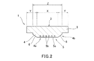
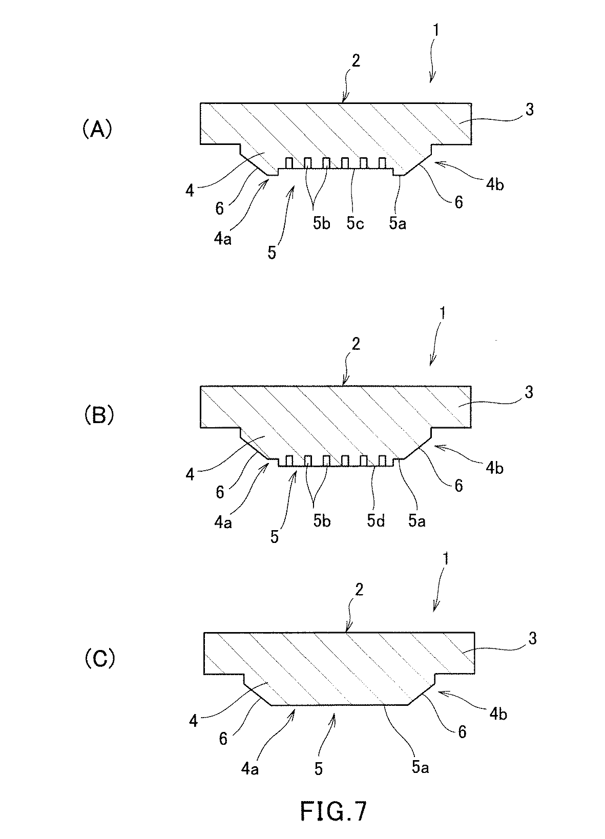
図1は本発明のナノインプリント用モールドの一実施形態を示す平面図であり、図2は図1に示されるナノインプリント用モールドのA−A線における断面図である。図1に示されるモールド1は、メサ構造のナノインプリント用モールドであり、基部3と、この基部3の一方の面から突出した凸構造部4とを有する透明な基材2と、凸構造部4の上面4aに位置する転写形状部5と、凸構造部4の側面4bの周囲方向全域に位置する傾斜部6(図1では斜線を付している)とを備えている。また、基材2は、パターン領域Xと、このパターン領域Xの周囲に位置する非パターン領域Yと、凸構造部領域Zに画定されている。この凸構造部領域Zは、凸構造部4が位置するとともに、ナノインプリント時にモールド1が被加工物に接触する可能性のある領域(最大領域)を示している。また、転写形状部5はパターン領域Xに位置し、傾斜部6はパターン領域Xの周囲の凸構造部領域Zに位置している。尚、図1では、凸構造部4の上面4aに位置する転写形状部5を構成する後述の凹部5bを省略している。
本発明のモールド1を構成する基材2は、被加工物を硬化させるための照射光を透過可能な透明基材である。このような基材2の材料としては、例えば、石英ガラス、珪酸系ガラス、フッ化カルシウム、フッ化マグネシウム、アクリルガラス等、あるいは、これらの任意の積層材を用いることができる。さらに、本発明のナノインプリント用モールドは、熱ナノインプリントにおいても同様の効果を奏するものであり、基材2の材料として、銅、ニッケル、鉄等の金属やその合金、または珪素を用いることができる。また、基材2の厚みは被加工物の材質、凸構造部4の形状、基材の強度、取り扱い適性等を考慮して設定することができ、例えば、300μm〜10mm程度の範囲で適宜設定することができる。
Hereinafter, embodiments of the present invention will be described with reference to the drawings.
FIG. 1 is a plan view showing an embodiment of a nanoimprint mold of the present invention, and FIG. 2 is a cross-sectional view taken along line AA of the nanoimprint mold shown in FIG. A
The
凸構造部4の上面4aに位置する転写形状部5は、図2に示される例では、上面4aと共通面をなす平坦面5aと、この平坦面5aに位置する凹部5bで構成されている。凹部5bは、ナノインプリントによって形成しようとするパターン形状の凹凸が反転した形状に対応した凹部であり、適宜設定することができ、エッチング等により形成することができる。
凸構造部4の側面4bに位置する傾斜部6は、ナノインプリント時に光照射が完了してモールド1を被加工物から離型する際に、硬化した被加工物とモールド1の側面との間に発生する摩擦力を低減し、離型に要する力(離型力)の変動を抑制して、モールドや被加工物に損傷が生じることを防止するためのものである。すなわち、モールド1を押し当てることで余剰となった被加工物は、パターン形成領域Xよりも外側(パターン領域Xの周囲の凸構造部領域Z)にはみ出し、凸構造部4の側面4bに付着する。そして、凸構造部4の側面4bに付着した被加工物は、パターン領域Xに位置する被加工物と同時に硬化する。このため、モールド1を離型する際に、硬化した被加工物と凸構造部4の側面4bとの間に摩擦力が発生するが、この摩擦力を傾斜部6により低減するものである。
In the example shown in FIG. 2, the
The
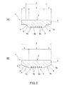
図3は、図1および図2に示されるナノインプリント用のモールド1の傾斜部6を説明するための部分拡大断面図である。図示例では、傾斜部6は、その開始部位6aが凸構造部4の上面4aと一致し、この上面4aに対し一定の角度θをなし、また、凸構造部4の側面4bの高さ方向(矢印aで示される方向)の一部を占めている。したがって、凸構造部4の側面4bは、この傾斜部6と、凸構造部4の上面4aに対して垂直(θ=90°)となっている側面4b′で構成されている。ここで、凸構造部4の側面4b全体が凸構造部4の上面4aに対して垂直(θ=90°)となっている場合(図8のモールド51を参照)に、硬化した被加工物と凸構造部4の側面4bとの間に生じる摩擦力をFとすると、硬化した被加工物と傾斜部6との間に生じる摩擦力はFsinθとなる。このため、傾斜部6が凸構造部4の上面4aに対してなす一定の角度θは小さいほど好ましいこととなり、パターン領域Xよりも外側に存在する凸構造部領域Zの幅W、凸構造部4の上面4aから傾斜部6の終了部位6bまでに要求される高さh等を考慮して適宜設定することができ、角度θは、例えば、10°〜60°の範囲内とすることができる。傾斜部6が凸構造部4の上面4aに対してなす角度θが60°を超えると、ナノインプリント用モールドを被加工物から離型する際に、硬化した被加工物とナノインプリント用モールドの側面との間に発生する摩擦力の低減が不充分なものとなり、離型に要する力(離型力)の変動が大きくなり、ナノインプリント用モールド1や被加工物への損傷が生じることがあり好ましくない。また、10°未満である場合、ナノインプリント装置におけるステージの平行度やナノインプリント用モールドの平行度の影響を受けやすく、本発明の効果である摩擦力の低減が不十分なものとなるため好ましくない。
FIG. 3 is a partially enlarged cross-sectional view for explaining the
ここで、凸構造部4の上面4aから傾斜部6の終了部位6bまでに要求される高さhは、パターン領域Xからはみ出した被加工物の高さに応じて設定され、被加工物へのモールド1の押し当て量(押し込み深さ)、被加工物の流動性、粘弾性等のほか、モールドとの濡れ性により決まる。この高さhのとりうる値の範囲について、詳細に検討する。
まず、高さhの上限は、凸構造部4の高さHに等しい。これは被加工物が傾斜部6にのみ接触している場合に摩擦力の低減が見込めるからである。パターン領域Xからはみ出した被加工物の高さが、高さhの上限(高さH)を超えてしまうような場合には、摩擦力を制御できない。この考え方を言い換えれば、被加工物がパターン領域Xからはみ出しても、傾斜部6にのみ接触していれば良いことになる。
Here, the height h required from the
First, the upper limit of the height h is equal to the height H of the
以上の考え方を基に、次に高さhの下限について検討する。モールド1の凹部5bを有する転写形状部5が被加工物に接触した際、被加工物は毛細管現象により凹部5b内部に入り込む場合がある。ただし傾斜部6では、モールドと被加工物との濡れ性によってメニスカスが形成されることになり、これが被加工物のはみ出しになる。このとき、被加工物は傾斜部6へはみ出していることから、はみ出した被加工物の高さは、凹部5bの深さdと比べて低くなり、実質的に平滑面と変わらなくなる。よって傾斜部6による摩擦力の低減効果を得るためには、モールドと被加工物とを接触させただけでなく、ごく僅かにでも力を加えてモールドを被加工物に押し込む必要が生じる。しかしこの場合、下記のように、樹脂の滴下量と、ナノインプリント装置の駆動制御性に起因する理由により、被加工物のはみ出し量を常に一定に制御することは困難となる。すなわち、例えば、被加工物として基板に供給した樹脂液滴の滴下量が10plであり、この液滴の直径が20〜30μmである場合、このような液滴サイズはナノインプリントにより得ようとするパターンサイズが仮に100nm程度とした場合であっても、非常に大きな数字である。このようにパターンサイズに比べて大きい直径の液滴を用いてモールドの凹部5bに樹脂を充填させ、かつ、はみ出す樹脂の量を制御しようとする場合、ナノインプリント装置内では、モールドと基板との平行度や、押し込み量の再現性等をナノスケールで制御しなければならない。したがって、被加工物のはみ出し量を常に一定に制御することは困難であり、これらを制御するよりも、モールドの傾斜部の高さhを大きくし、被加工物がはみ出る空間に余裕をとる方が、実用上は平易であり、好ましい。ここで、傾斜部6が凸構造部4の上面4aに対してなす角度θの範囲が、上記のように、10°〜60°の範囲内であることから、被加工物は水平方向に広がる。よって被加工物がはみ出る量を考慮すると、高さhは、凹部5bの最大深さdmaxよりも大きい必要がある。
Next, the lower limit of the height h is examined based on the above concept. When the
上記のような検討から、高さhと、凹部5bの最大深さd、凸構造部4の高さHと間にdmax<h≦Hの関係が成立する。更に水平方向へはみ出た樹脂を広げる場合、高さhを十分大きくし、樹脂がはみ出すことが可能な空間を確保しておく必要がある。よって高さhは、好ましくは凹部5bの最大深さdmaxの50倍以上となるように設定することが望ましい。
また、高さhは、凸構造部4の高さ方向で、傾斜部6の終了部位6bと凹部5bの最深部とが10μm以上、好ましくは15μm以上離間するように設定することができる。このような高さhが上記の範囲未満であると、モールド1を押し当てることで余剰となりパターン形成領域Xよりも外側(パターン領域Xの周囲の凸構造部領域Z)にはみ出した被加工物が傾斜部6を超え、凸構造部4の上面4aに対して垂直(θ=90°)となっている側面4b′に付着し、本発明の効果に支障を来すことがある。
上記のように凸構造部4の側面4bの周囲方向全域に位置する傾斜部6は、例えば、凸構造部4の周縁部をマスクエッチング、ラッピングやポリッシング、バフ研磨等により研磨することにより形成することができる。上記のように、傾斜部6が上面4aに対して一定の角度θをなしている場合、モールド1を被加工物から離型する際に、傾斜部6から被加工物が剥がれる動作中に傾斜部6と被加工物との間に作用する摩擦力が一定となるので、離型力のバラツキが低減される。
From the above examination, the relationship of dmax <h ≦ H is established between the height h, the maximum depth d of the
Further, the height h can be set so that the
As described above, the
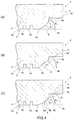
本発明では、上記の傾斜部6は図3に示される形状に限定されるものではなく、傾斜部6が凸構造部4の上面4aに対してなす角度θが一定でないものであってもよい。例えば、図4(A)に示されるように、傾斜部6が凸面形状であってもよい。この例では、凸構造部4の上面4aから傾斜部6が開始する部位6aにおける上面4aに対する角度がθ1であり、傾斜部6の終了部位6bにおける上面4aに対する角度がθ2であり、上面4aに対する角度は、角度θ1から角度θ2まで徐々に大きくなっている。このような実施形態においても、凸構造部4の上面4aに対する傾斜部6の角度は上記の例と同様に設定することがでる。例えば、(θ1+θ2)/2を60°以下、好ましくは45°以下とすることができ、より好ましくは、最も大きい角度θ2を45°以下とすることができる。
また、図4(B)に示されるように、傾斜部6が凹面形状であってもよい。この例では、凸構造部4の上面4aから傾斜部6が開始する部位6aにおける上面4aに対する角度がθ1であり、傾斜部6の終了部位6bにおける上面4aに対する角度がθ2であり、上面4aに対する角度は、角度θ1から角度θ2まで徐々に小さくなっている。このような態様においても、凸構造部4の上面4aに対する傾斜部6の角度は上記の例と同様に設定することがでる。例えば、(θ1+θ2)/2を60°以下、好ましくは45°以下とすることができ、より好ましくは、最も大きい角度θ1を45°以下とすることができる。
In the present invention, the
Further, as shown in FIG. 4B, the
さらに、傾斜部6が段階的に角度が変化する凸面形状、あるいは、凹面形状であってもよく、このような例として、凸面形状の例を図4(C)に示す。図4(C)に示されるように、凸構造部4の上面4aから傾斜部6が開始する面6Aにおける上面4aに対する角度がθ1であり、この面6Aに続く面6Bが上面4aに対する角度がθ2であり、この面6Bに続く面6Cにおける上面4aに対する角度がθ3であり、上面4aに対する角度は、角度θ1から角度θ3まで段階的に大きくなっている。このような態様においても、凸構造部4の上面4aに対する傾斜部6A,6B,6Cの角度は上記の例と同様に設定することがでる。例えば、(θ1+θ2+θ3)/3を60°以下、好ましくは45°以下とすることができ、より好ましくは、最も大きい角度θ3を45°以下とすることができる。
このように、凸構造部4の上面4aに対する角度に変化を有する傾斜部6は、例えば、ウェットエッチング、ラッピングやポリッシング、バフ研磨等により研磨することによって形成することができる。そして、図4(A)、図4(C)に示すように、傾斜部6が凸面形状である場合、モールド1と被加工物との離型において、両者の剥離が生じる箇所が傾斜部6を外側から内側へ移行して上面4aに近づくにしたがって角度θが小さくなり、応力発生を抑制することができ、被加工物の破損を抑えることができる。
Further, the
Thus, the
また、凸構造部4の側面4bに占める傾斜部6は、上記の図3、図4(A)〜図4(C)に示される形態に限定されるものではない。例えば、図5(A)に示されるように、凸構造部4の側面4bの高さ方向の全面が傾斜部6(図3においてh=H)であってもよい。さらに、凸構造部領域Zが基材2の全域に亘る場合(Z=X+Y)の場合、図5(B)に示されるように、傾斜部6の終了する部位6bが基材2(基部3)の端部に位置するものであってもよい。
In addition, the
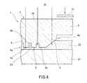
次に、このようなナノインプリント用のモールド1を用いたインプリント装置によるナノインプリントでのパターン形成の一例を図6を参照して説明する。
図6に示されるように、基板21の表面に被加工物として配設された光硬化性の樹脂層22に、モールド1の凸構造部4を所定の深さまで押し込む。そして、この状態で照明光学系(図示せず)から遮光マスク31を介してモールド1の裏面2bに紫外線を照射し、モールド1を透過した紫外線により樹脂層22を硬化させる。このとき、パターン領域Xに位置する樹脂層22とともに、凸構造部領域Zに位置する樹脂層22も硬化される。
その後、ナノインプリント用のモールド1を樹脂層22から離型することにより、モールド1が有する凹部5bが反転した凹凸構造(凹凸パターン)23が被加工物である樹脂層22に転写形成される。この離型の際、パターン領域Xの外側に位置する硬化された樹脂層22は、モールド1の傾斜部6に接触しているので、硬化した樹脂層22とモールド1との間に発生するモールド側面の傾斜に対して平行に働く力(摩擦力)が低減され、離型に要する力(離型力)の変動が抑制される。これにより、ナノインプリント用モールド1や被加工物22への損傷が防止され、微細な凹凸構造(凹凸パターン)23を安定して形成することができる。
Next, an example of pattern formation by nanoimprinting by an imprinting apparatus using such a
As shown in FIG. 6, the
Thereafter, the
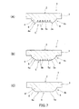
上述の実施形態は例示であり、本発明はこれに限定されるものではない。例えば、凸構造部4の上面4aに位置する転写形状部5は、図2に示されるものに限定されものではなく、図7(A)に示されるように、上面4aと共通面をなす平坦面5aと、凹平面5cと、この凹平面5cに位置する凹部5bで構成されるものであってもよい。また、図7(B)に示されるように、上面4aと共通面をなす平坦面5aと、凸平面5dと、この凸平面5dに位置する凹部5bで構成されるもの、さらに、図7(C)に示されるように、上面4aと共通面をなす平坦面5aのみで構成されるものであってもよい。
The above-described embodiment is an exemplification, and the present invention is not limited to this. For example, the
次に、より具体的な実施例を示して本発明を更に詳細に説明する。
[実施例1]
厚み6.35mmの石英ガラス(65mm角)をナノインプリント用モールド用基材として準備した。
次に、この基材の周縁部(端部から12.5mmの幅)をバフ研磨することにより、図5(B)に示されるような傾斜部を形成した。この傾斜部が凸構造部の上面(40mm角)となす角度は60°(一定)であり、凸構造部の上面から傾斜部の終了部位までの高さh(図5(B)参照)は4mmであった。
Next, the present invention will be described in more detail by showing more specific examples.
[Example 1]
Quartz glass (65 mm square) with a thickness of 6.35 mm was prepared as a base material for a mold for nanoimprinting.
Next, an inclined portion as shown in FIG. 5B was formed by buffing the peripheral portion (width of 12.5 mm from the end portion) of the base material. The angle formed by the inclined portion with the upper surface (40 mm square) of the convex structure portion is 60 ° (constant), and the height h from the upper surface of the convex structure portion to the end portion of the inclined portion (see FIG. 5B) is It was 4 mm.
次に、上記の基材上に市販の感光性レジストを塗布し、凸構造部の上面に位置する感光性レジストを電子線描画により露光、現像して、ピッチ200nm、パターン幅100nmのLSパターンのレジストパターンを形成した。このレジストパターンをマスクとし、凸構造部の上面を下記の条件でドライエッチングして、深さ100nmの凹部を形成して転写形状部とした。
(ドライエッチング条件)
・エッチングガス : CF4
・ガス流量 : 40sccm
・チャンバー圧力 : 4Pa
・投入RF電力 : 400W
これにより、図5(B)に示されるようなナノインプリント用モールドを得た。
Next, a commercially available photosensitive resist is applied onto the substrate, and the photosensitive resist located on the upper surface of the convex structure portion is exposed and developed by electron beam drawing to form an LS pattern having a pitch of 200 nm and a pattern width of 100 nm. A resist pattern was formed. Using this resist pattern as a mask, the upper surface of the convex structure portion was dry-etched under the following conditions to form a recess having a depth of 100 nm to form a transfer shape portion.
(Dry etching conditions)
Etching gas: CF 4
・ Gas flow rate: 40sccm
・ Chamber pressure: 4Pa
・ Input RF power: 400W
Thereby, a mold for nanoimprinting as shown in FIG. 5B was obtained.
[比較例]
ナノインプリント用モールド用基材の周縁部(端部から12.5mmの幅)に対してドライエッチングによるメサ加工を行い、高さ15μmの凸構造部(40mm角)を形成し、この凸構造部の外周部には傾斜部を形成しない以外は、実施例1と同様にして、図8に示されるようなナノインプリント用モールドを作製した。
[Comparative example]
The mesa processing by dry etching is performed on the peripheral part (width of 12.5 mm from the end part) of the nanoimprint mold base material to form a convex structure part (40 mm square) with a height of 15 μm. A nanoimprint mold as shown in FIG. 8 was produced in the same manner as in Example 1 except that the inclined portion was not formed on the outer peripheral portion.
<評 価>
このように作製したナノインプリント用モールド(実施例、比較例)を用いて、下記のように、ナノインプリントを行った。
すなわち、厚み625μmの石英ウエハ上に光硬化性樹脂(東洋合成工業(株)製 PAK−01)を塗布して被加工物とし、石英ウエハ側が当接するようにインプリント装置の基板ステージに載置した。次いで、光硬化性樹脂層にモールドを押し込んだ。このときの光硬化性樹脂層へのモールドのプレス力は1kNであり、比較例のモールドにおける凸構造部の高さ(15μm)よりも小さいものとした。この状態でインプリント装置の照明光学系から平行光(ピーク波長が365nmの紫外線)を100mJ/cm2照射した。これにより、光硬化性樹脂層を硬化させ、その後、モールドを引き離してパターンを形成した。
<Evaluation>
Using the nanoimprint mold (Examples and Comparative Examples) produced in this manner, nanoimprinting was performed as follows.
That is, a photocurable resin (PAK-01 manufactured by Toyo Gosei Kogyo Co., Ltd.) is applied on a quartz wafer having a thickness of 625 μm to form a workpiece, and placed on the substrate stage of the imprint apparatus so that the quartz wafer side contacts. did. Next, a mold was pushed into the photocurable resin layer. At this time, the pressing force of the mold to the photocurable resin layer was 1 kN, which was smaller than the height (15 μm) of the convex structure portion in the mold of the comparative example. In this state, 100 mJ / cm 2 of parallel light (ultraviolet light having a peak wavelength of 365 nm) was irradiated from the illumination optical system of the imprint apparatus. Thereby, the photocurable resin layer was cured, and then the pattern was formed by separating the mold.
このようなパターン形成を各モールドで10回行い、モールドを引き離す際に要した力(N)をナノインプリント装置に内蔵されたロードセルを用いて測定し、この測定値(N)を樹脂とモールドが接触した面積(mm2)で除すことにより離型力(MPa)を算出し、その平均値と変動量(最大値と最小値の差)を表1に示した。また、形成されたパターンについて、欠陥率を下記のように測定し、その結果を表1に示した。
(欠陥率の測定)
光学顕微鏡で各パターンについて5箇所観察し、一つの観察箇所(1.0mm×1.0mm)内で、パターン欠損が確認できた面積の割合を測定し、100個のパターン、計500箇所の平均を算出した。したがって、この欠陥率が大きい程、欠陥が多いことを意味し、本発明では、欠陥率が0.1未満を実用レベルと判定する。
Such pattern formation is performed 10 times for each mold, and the force (N) required for separating the molds is measured using a load cell built in the nanoimprint apparatus, and the measured value (N) is contacted between the resin and the mold. The release force (MPa) was calculated by dividing by the measured area (mm 2 ), and the average value and the fluctuation amount (difference between the maximum value and the minimum value) are shown in Table 1. Moreover, the defect rate was measured about the formed pattern as follows, and the result was shown in Table 1.
(Defect rate measurement)
Observe five patterns for each pattern with an optical microscope, and measure the ratio of the area where pattern defects were confirmed within one observation spot (1.0 mm × 1.0 mm). The average of 100 patterns and a total of 500 spots. Was calculated. Therefore, it means that there are many defects, so that this defect rate is large, and in this invention, it determines with a defect rate being less than 0.1 as a practical use level.
ナノインプリント技術を用いた微細加工に利用可能である。 It can be used for microfabrication using nanoimprint technology.
1…ナノインプリント用モールド
2…基材
3…基部
4…凸構造部
4a…上面
4b…側面
5…転写形状部
6…傾斜部
X…パターン領域
Y…非パターン領域
Z…凸構造部領域
DESCRIPTION OF
Claims (7)
前記転写形状部は、前記上面と共通面をなす平坦面と該平坦面に位置する凹部で構成されるもの、前記上面と共通面をなす平坦面と前記上面よりも凹状態にある凹平面と該凹平面に位置する凹部で構成されるもの、前記上面と共通面をなす平坦面と前記上面よりも凸状態にある凸平面と該凸平面に位置する凹部であって深さが前記上面からの前記凸平面の凸状態の高さよりも大きい凹部で構成されるもの、および、前記上面と共通面をなす平坦面で構成されるもののいずれかであり、
前記傾斜部は前記凸構造部の側面の高さ方向の一部を占め、傾斜部の開始部位は前記凸構造部の上面と共通面をなす前記平坦面と一致し、前記傾斜部を除く前記凸構造部の側面は前記凸構造部の上面に対して垂直となっていることを特徴とするナノインプリント用モールド。 A base having a base and a convex structure protruding from one surface of the base; a transfer shape positioned on the upper surface of the convex structure; and an inclined portion positioned in the entire circumferential direction of the side surface of the convex structure And comprising
The transfer shape portion includes a flat surface that forms a common surface with the upper surface and a concave portion that is located on the flat surface, a flat surface that forms a common surface with the upper surface, and a concave plane that is more concave than the upper surface. A concave surface located on the concave plane, a flat surface that forms a common surface with the upper surface, a convex surface that is more convex than the upper surface, and a concave portion that is positioned on the convex plane, the depth of which is from the upper surface Or a concave portion larger than the height of the convex state of the convex plane , or a flat surface that forms a common surface with the upper surface,
The inclined portion occupies a part of the height direction of the side surface of the convex structure portion, and the start portion of the inclined portion coincides with the flat surface that forms a common surface with the upper surface of the convex structure portion, and excludes the inclined portion. The side surface of a convex structure part is perpendicular | vertical with respect to the upper surface of the said convex structure part, The mold for nanoimprint characterized by the above-mentioned.
前記ナノインプリント用モールドの転写形成部を前記液滴と接触させて光硬化性の前記樹脂層を形成する際に、光硬化性の前記樹脂層が前記凸構造部の傾斜部と接触し、前記傾斜部を除く前記凸構造部の側面には接触しないように制御することを特徴とするパターン形成方法。 A photocurable resin droplet is supplied to a substrate, and the nanoimprint mold according to any one of claims 1 to 5 is brought into contact with the droplet to form a photocurable resin layer. And curing the photocurable resin layer, and then releasing the cured resin layer and the mold,
When the photocurable resin layer is formed by bringing the transfer forming portion of the nanoimprint mold into contact with the droplets, the photocurable resin layer is in contact with the inclined portion of the convex structure portion, and the inclined A pattern forming method characterized by controlling so as not to contact a side surface of the convex structure portion excluding the portion.
Priority Applications (1)
| Application Number | Priority Date | Filing Date | Title |
|---|---|---|---|
| JP2010143418A JP5978552B2 (en) | 2010-06-24 | 2010-06-24 | Nanoimprint mold and pattern forming method |
Applications Claiming Priority (1)
| Application Number | Priority Date | Filing Date | Title |
|---|---|---|---|
| JP2010143418A JP5978552B2 (en) | 2010-06-24 | 2010-06-24 | Nanoimprint mold and pattern forming method |
Publications (2)
| Publication Number | Publication Date |
|---|---|
| JP2012006219A JP2012006219A (en) | 2012-01-12 |
| JP5978552B2 true JP5978552B2 (en) | 2016-08-24 |
Family
ID=45537356
Family Applications (1)
| Application Number | Title | Priority Date | Filing Date |
|---|---|---|---|
| JP2010143418A Active JP5978552B2 (en) | 2010-06-24 | 2010-06-24 | Nanoimprint mold and pattern forming method |
Country Status (1)
| Country | Link |
|---|---|
| JP (1) | JP5978552B2 (en) |
Cited By (1)
| Publication number | Priority date | Publication date | Assignee | Title |
|---|---|---|---|---|
| US11541577B2 (en) | 2019-12-18 | 2023-01-03 | Canon Kabushiki Kaisha | Template apparatus and methods of using the same |
Families Citing this family (10)
| Publication number | Priority date | Publication date | Assignee | Title |
|---|---|---|---|---|
| JP5821409B2 (en) * | 2011-08-24 | 2015-11-24 | 大日本印刷株式会社 | Mold for nanoimprint lithography |
| JP5823937B2 (en) * | 2012-09-07 | 2015-11-25 | 株式会社東芝 | MOLD, MOLD BLANK SUBSTRATE, AND MOLD MANUFACTURING METHOD |
| JP6136271B2 (en) * | 2013-01-08 | 2017-05-31 | 大日本印刷株式会社 | Manufacturing method of imprint mold |
| JP6102519B2 (en) * | 2013-05-28 | 2017-03-29 | 大日本印刷株式会社 | Template substrate, template blank, template for nanoimprint, method for producing template substrate, and method for regenerating template substrate |
| SG11201604509UA (en) * | 2013-12-10 | 2016-07-28 | Canon Nanotechnologies Inc | Imprint lithography template and method for zero-gap imprinting |
| JP6398284B2 (en) * | 2014-04-21 | 2018-10-03 | 大日本印刷株式会社 | Imprint mold, blank for imprint mold, method for producing imprint mold substrate, and method for producing imprint mold |
| JP2016157785A (en) | 2015-02-24 | 2016-09-01 | 株式会社東芝 | Template forming method, template, and template base material |
| JP6957917B2 (en) * | 2017-03-21 | 2021-11-02 | 大日本印刷株式会社 | Mask blank for imprint mold and its manufacturing method, imprint mold and its manufacturing method, and imprint method |
| JP2019161020A (en) * | 2018-03-13 | 2019-09-19 | キヤノン株式会社 | Mold, imprint apparatus, and article manufacturing method |
| JP2019212862A (en) * | 2018-06-08 | 2019-12-12 | キヤノン株式会社 | Mold, planar plate, imprint method, and article manufacturing method |
Family Cites Families (8)
| Publication number | Priority date | Publication date | Assignee | Title |
|---|---|---|---|---|
| JPH0832420B2 (en) * | 1987-12-28 | 1996-03-29 | キヤノン株式会社 | Casting mold and method for manufacturing substrate for information recording medium using the same |
| JP4340086B2 (en) * | 2003-03-20 | 2009-10-07 | 株式会社日立製作所 | Nanoprinting stamper and fine structure transfer method |
| JP2005101233A (en) * | 2003-09-24 | 2005-04-14 | Sankyo Seiki Mfg Co Ltd | Mold manufacturing method, mold, and molded product |
| JP4996150B2 (en) * | 2006-07-07 | 2012-08-08 | 株式会社日立ハイテクノロジーズ | Fine structure transfer apparatus and fine structure transfer method |
| JP5182470B2 (en) * | 2007-07-17 | 2013-04-17 | 大日本印刷株式会社 | Imprint mold |
| JP4815464B2 (en) * | 2008-03-31 | 2011-11-16 | 株式会社日立製作所 | Fine structure transfer stamper and fine structure transfer apparatus |
| JP5161707B2 (en) * | 2008-08-28 | 2013-03-13 | 株式会社日立産機システム | MICROSTRUCTURE TRANSFER MOLD AND MICROSTRUCTURE TRANSFER APPARATUS |
| JP2010094845A (en) * | 2008-10-14 | 2010-04-30 | Dainippon Printing Co Ltd | Method of manufacturing pattern forming body, and method of manufacturing mold for nano-printing |
-
2010
- 2010-06-24 JP JP2010143418A patent/JP5978552B2/en active Active
Cited By (1)
| Publication number | Priority date | Publication date | Assignee | Title |
|---|---|---|---|---|
| US11541577B2 (en) | 2019-12-18 | 2023-01-03 | Canon Kabushiki Kaisha | Template apparatus and methods of using the same |
Also Published As
| Publication number | Publication date |
|---|---|
| JP2012006219A (en) | 2012-01-12 |
Similar Documents
| Publication | Publication Date | Title |
|---|---|---|
| JP5978552B2 (en) | Nanoimprint mold and pattern forming method | |
| JP4406452B2 (en) | Belt-shaped mold and nanoimprint apparatus using the same | |
| JP5935385B2 (en) | Method of manufacturing replica template for nanoimprint and replica template | |
| JP5942551B2 (en) | Manufacturing method of master template and replica template for nanoimprint | |
| JP5935453B2 (en) | Substrate manufacturing method and nanoimprint lithography template manufacturing method | |
| JP6019685B2 (en) | Nanoimprint method and nanoimprint apparatus | |
| JP5480530B2 (en) | Fine structure transfer method and fine structure transfer apparatus | |
| JP2019080047A (en) | Imprint device and article manufacturing method | |
| JP2012200988A (en) | Method for removing foreign matter adhered to mold | |
| JP2011116032A (en) | Mold for imprinting and method for forming pattern using this mold | |
| JP5114962B2 (en) | Imprint mold, imprint evaluation apparatus using the same, resist pattern forming method, and imprint mold manufacturing method | |
| JP2007266384A (en) | Imprint mold and manufacturing method thereof | |
| TW201535044A (en) | Patterning method and manufacturing method of patterning substrate | |
| JP2013033878A (en) | Template for semiconductor imprint | |
| JP6281592B2 (en) | Manufacturing method of replica template | |
| US20080217819A1 (en) | Micro/Nano-Pattern Film Contact Transfer Process | |
| JP6155720B2 (en) | Nanoimprint template pattern arrangement method and nanoimprint template | |
| JP5747670B2 (en) | Molded member and manufacturing method thereof | |
| JP6106949B2 (en) | Pattern formation method | |
| JP5200726B2 (en) | Imprint method, pre-imprint mold, pre-imprint mold manufacturing method, imprint apparatus | |
| JP2016149578A (en) | Production method of replica template for nanoimprinting | |
| JP5295870B2 (en) | Imprint pattern forming method | |
| JP2020111065A (en) | Filler-filled film, single-wafer film, laminated film, bonded body, and method for manufacturing filler-filled film | |
| JP2007253577A (en) | Imprint mold member, imprint mold member manufacturing method, and imprint method | |
| JP2014011431A (en) | Microstructure transcription device, microstructure transcription stamper, and microstructure transcription method |
Legal Events
| Date | Code | Title | Description |
|---|---|---|---|
| A621 | Written request for application examination |
Free format text: JAPANESE INTERMEDIATE CODE: A621 Effective date: 20130425 |
|
| A977 | Report on retrieval |
Free format text: JAPANESE INTERMEDIATE CODE: A971007 Effective date: 20140424 |
|
| A131 | Notification of reasons for refusal |
Free format text: JAPANESE INTERMEDIATE CODE: A131 Effective date: 20140430 |
|
| A521 | Written amendment |
Free format text: JAPANESE INTERMEDIATE CODE: A523 Effective date: 20140613 |
|
| A131 | Notification of reasons for refusal |
Free format text: JAPANESE INTERMEDIATE CODE: A131 Effective date: 20150120 |
|
| A521 | Written amendment |
Free format text: JAPANESE INTERMEDIATE CODE: A523 Effective date: 20150306 |
|
| A131 | Notification of reasons for refusal |
Free format text: JAPANESE INTERMEDIATE CODE: A131 Effective date: 20151013 |
|
| A131 | Notification of reasons for refusal |
Free format text: JAPANESE INTERMEDIATE CODE: A131 Effective date: 20160419 |
|
| A521 | Written amendment |
Free format text: JAPANESE INTERMEDIATE CODE: A523 Effective date: 20160603 |
|
| TRDD | Decision of grant or rejection written | ||
| A01 | Written decision to grant a patent or to grant a registration (utility model) |
Free format text: JAPANESE INTERMEDIATE CODE: A01 Effective date: 20160628 |
|
| A61 | First payment of annual fees (during grant procedure) |
Free format text: JAPANESE INTERMEDIATE CODE: A61 Effective date: 20160711 |
|
| R150 | Certificate of patent or registration of utility model |
Ref document number: 5978552 Country of ref document: JP Free format text: JAPANESE INTERMEDIATE CODE: R150 |