JP2007253577A - Mold member for imprint, manufacturing method therefor, and imprint method - Google Patents
Mold member for imprint, manufacturing method therefor, and imprint method Download PDFInfo
- Publication number
- JP2007253577A JP2007253577A JP2006084347A JP2006084347A JP2007253577A JP 2007253577 A JP2007253577 A JP 2007253577A JP 2006084347 A JP2006084347 A JP 2006084347A JP 2006084347 A JP2006084347 A JP 2006084347A JP 2007253577 A JP2007253577 A JP 2007253577A
- Authority
- JP
- Japan
- Prior art keywords
- substrate
- mold member
- imprint
- mold
- pattern
- Prior art date
- Legal status (The legal status is an assumption and is not a legal conclusion. Google has not performed a legal analysis and makes no representation as to the accuracy of the status listed.)
- Granted
Links
Images


Abstract
Description
本発明は、微細なパターン形成を行うためのインプリント用型部材、インプリント用型部材の製造方法、及びインプリント方法に関する。 The present invention relates to an imprint mold member for forming a fine pattern, a method for manufacturing an imprint mold member, and an imprint method.
一般に、半導体デバイス、光導波路や回折格子等の光学部品、ハードディスクやDVD等の記録デバイス、DNA分析等のバイオチップ、拡散版や導光版などのディスプレイ等の製造プロセスにて微細加工が要求されるパターンの形成には、光学的にパターンを転写する方法(フォトリソグラフィ)が用いられている。 Generally, microfabrication is required in the manufacturing process of semiconductor devices, optical components such as optical waveguides and diffraction gratings, recording devices such as hard disks and DVDs, biochips such as DNA analysis, and displays such as diffusion plates and light guide plates. In order to form a pattern, an optical pattern transfer method (photolithography) is used.
しかしながら、このようなパターン形成方法では、形成するパターンのサイズや形状が露光する光の波長に大きく依存する。例えば、先端的な半導体デバイスの製造においては、フォトリソグラフィに用いる露光波長は150nm以上であるのに対し、最小線幅は65nm以下であり、光の回折現象による解像限界に達している。 However, in such a pattern forming method, the size and shape of the pattern to be formed greatly depend on the wavelength of light to be exposed. For example, in the manufacture of advanced semiconductor devices, the exposure wavelength used for photolithography is 150 nm or more, while the minimum line width is 65 nm or less, reaching the resolution limit due to the light diffraction phenomenon.
そこで、レジストの解像度を増すために、近接効果補正(OPC:Optical Proximity Correction)や位相シフトマスク、変形照明等の超解像技術が用いられている。しかし、マスクパターンを半導体基板上に忠実に転写することが困難となっている。また、マスクや露光装置価格の高騰の問題を抱えている。 Therefore, in order to increase the resolution of the resist, super-resolution techniques such as proximity effect correction (OPC: Optical Proximity Correction), a phase shift mask, and modified illumination are used. However, it is difficult to faithfully transfer the mask pattern onto the semiconductor substrate. In addition, there is a problem of rising prices of masks and exposure apparatuses.
フォトリソグラフィ法を用いている限り、半導体デバイスの製造のみならず、ディスプレイや記録メディア、バイオチップ、光デバイスなど様々なパターン形成においても、これらの光の回折現象によるパターンボケや複雑な機構を必要とする装置コストの問題が同様に存在し、マスクパターンを忠実に転写することが出来ない。 As long as the photolithography method is used, not only the manufacture of semiconductor devices, but also the formation of various patterns such as displays, recording media, biochips, and optical devices requires pattern blurring and complicated mechanisms due to the diffraction phenomenon of these lights. Similarly, there is a problem of the apparatus cost, and the mask pattern cannot be transferred faithfully.
このような背景から、インプリント法(もしくはナノインプリント法)と呼ばれる非常に簡易であるが大量生産に向き、従来の方法よりも格段に微細なパターンを忠実に転写可能な技術が提案されている(例えば、非特許文献1参照。)。
Against this background, a technique called imprint method (or nanoimprint method), which is very simple but suitable for mass production, has been proposed which can faithfully transfer a much finer pattern than conventional methods ( For example, refer
ここで、インプリント法には、大きく分けて光インプリントと熱インプリントとの二種類が提案されている。ここでは、光インプリントによるパターン形成方法について説明する。 Here, two types of imprint methods, optical imprint and thermal imprint, have been proposed. Here, a pattern forming method by optical imprinting will be described.
具体的には、石英などの透光性を有する材料からなるモールド基板(型部材作製用素材)を電子ビームリソグラフィ法などにより露光、現像し、図6(a)に示すようにエッチングにより表面に凹凸のパターン100を有するモールド(型部材)101を作製する。次に、図6(b)に示すように、パターン形成させる基板102上に粘度の低い液体状のレジスト(光硬化性樹脂組成物)103を塗布し、図6(c)に示すように、モールド101をレジスト103に圧着させる。このときのプレス圧力は0.01〜5MPa程度と小さくて良い。
Specifically, a mold substrate (material for forming a mold member) made of a light-transmitting material such as quartz is exposed and developed by an electron beam lithography method or the like, and is etched on the surface as shown in FIG. A mold (mold member) 101 having an
この状態で、モールド101の裏面から光を照射し、図6(d)に示すように、レジスト103を硬化させる。そして、モールド101を離型し、パターン100が転写されたレジスト103の薄い残膜をO2反応性イオンエッチング(RIE)法などにより除去することによって、図6(e) に示すように、基板102上に転写パターン105が形成される。
しかしながら、上記従来のインプリント用型部材を用いてインプリントする場合、モールドの凹部が垂直に形成されていても、光硬化性樹脂を硬化する際に収縮が起こり、図6(e)に示すように、転写パターンが傾斜した形状となってしまい、所望する形状や寸法のものが得られないという問題がある。 However, when imprinting using the above-described conventional imprint mold member, even when the concave portion of the mold is formed vertically, shrinkage occurs when the photocurable resin is cured, as shown in FIG. As described above, there is a problem that the transfer pattern has an inclined shape, and a desired shape and size cannot be obtained.
そのため、このパターンをエッチングしても、形状不良によりエッチング後に所望の寸法が得られない。また、ラインエッジラフネスが悪化してしまうなどの品質の低下や、それに伴う歩留まりを引き起こしてしまう。 Therefore, even if this pattern is etched, a desired dimension cannot be obtained after etching due to a shape defect. In addition, the quality deteriorates, such as the line edge roughness being deteriorated, and the yield is accordingly increased.
本発明は上記事情に鑑みて成されたものであり、基板上に垂直形状に立設された転写パターンが得られるインプリント用型部材、インプリント用型部材の製造方法、及びこのインプリント用型部材を用いたインプリント方法を提供することを目的とする。 The present invention has been made in view of the above circumstances, and an imprint mold member capable of obtaining a transfer pattern erected vertically on a substrate, a method for manufacturing the imprint mold member, and the imprint It is an object of the present invention to provide an imprint method using a mold member.
本発明は、上記課題を解決するため、以下の手段を採用する。
本発明に係るインプリント用型部材は、表面に基板用光硬化性樹脂が配設された基板を押圧して、一表面に形成された凹部と凸部とからなるパターンを前記基板に転写するためのインプリント用型部材であって、前記凹部が、前記一表面から深さ方向に漸次拡開して設けられていることを特徴とする。
The present invention employs the following means in order to solve the above problems.
The imprint mold member according to the present invention presses a substrate having a photocurable resin for a substrate disposed on the surface thereof, and transfers a pattern composed of concave and convex portions formed on one surface to the substrate. The imprint mold member is characterized in that the concave portion is provided so as to gradually expand in the depth direction from the one surface.
この発明は、基板用光硬化性樹脂が配設された基板表面に一表面を押圧したときに、凹部内に圧入された基板上の基板用光硬化性樹脂を、基板側からインプリント用型部材の内部に向かって漸次拡開するように立設させることができる。この際、基板用光硬化性樹脂を硬化させることによって樹脂の先端側が基板側よりも収縮するので、硬化した樹脂を最終的に垂直方向に立設させることができる。 The present invention relates to an imprint mold for imprinting a photocurable resin for a substrate on a substrate press-fitted into a recess when the surface is pressed against the substrate surface on which the photocurable resin for a substrate is disposed. It can stand up so that it may expand gradually toward the inside of a member. At this time, by curing the photo-curing resin for the substrate, the front end side of the resin contracts more than the substrate side, so that the cured resin can be finally erected in the vertical direction.
また、本発明に係るインプリント用型部材は、前記インプリント用型部材であって、透明部材からなる型部材作製用素材から構成されていることを特徴とする。 Moreover, the imprint mold member according to the present invention is the imprint mold member, and is characterized in that it is made of a mold member manufacturing material made of a transparent member.
この発明は、型部材作製用素材が透光性を有するので、型部材の裏面から露光して基板上の光硬化性樹脂を硬化させることができる。 In this invention, since the material for producing the mold member has translucency, the photocurable resin on the substrate can be cured by exposure from the back surface of the mold member.
また、本発明に係るインプリント用型部材の製造方法は、基板用光硬化性樹脂が配設された基板表面を押圧して、一表面に形成された凹部と凸部とからなるパターンを転写するためのインプリント用型部材の製造方法であって、前記型用光硬化性樹脂を硬化させた後、ドライエッチングによって前記インプリント用型部材の前記一表面から深さ方向に漸次拡開した凹部を形成する工程を備えていることを特徴とする。 Also, the method for manufacturing an imprint mold member according to the present invention presses a substrate surface on which a substrate photocurable resin is disposed, and transfers a pattern formed of a concave portion and a convex portion formed on one surface. A method for producing an imprint mold member for curing, wherein the mold photocurable resin is cured, and then gradually spread in the depth direction from the one surface of the imprint mold member by dry etching. A step of forming a recess is provided.
また、本発明に係るインプリント用型部材の製造方法は、基板用光硬化性樹脂が配設された基板表面を押圧して、一表面に形成された凹部と凸部とからなるパターンを転写するためのインプリント用型部材の製造方法であって、収束イオンビームを用いて前記インプリント用型部材の前記一表面から深さ方向に漸次拡開した凹部を形成する工程を備えていることを特徴とする。 Also, the method for manufacturing an imprint mold member according to the present invention presses a substrate surface on which a substrate photocurable resin is disposed, and transfers a pattern formed of a concave portion and a convex portion formed on one surface. A method for producing an imprint mold member for forming a concave portion that gradually expands in the depth direction from the one surface of the imprint mold member using a focused ion beam. It is characterized by.
この発明は、型部材作製用素材に対して、所望の傾斜角度で一表面から深さ方向に漸次拡開する凹部を高精度に加工することができる。 According to the present invention, a concave portion that gradually expands in a depth direction from one surface at a desired inclination angle can be processed with high accuracy with respect to a mold member manufacturing material.
また、本発明に係るインプリント用型部材の製造方法は、前記インプリント用型部材の製造方法であって、前記凹部の深さと幅とのアスペクト比、及び前記基板用光硬化性樹脂の体積収縮率から前記凹部の傾斜角度を決める工程を備えていることを特徴とする。 Further, the imprint mold member manufacturing method according to the present invention is a method for manufacturing the imprint mold member, wherein the aspect ratio between the depth and the width of the concave portion, and the volume of the photocurable resin for the substrate. A step of determining the inclination angle of the recess from the shrinkage rate is provided.
この発明は、基板上の基板用光硬化性樹脂を硬化収縮後に垂直方向に立設させることができる。 According to the present invention, a photocurable resin for a substrate on a substrate can be erected in a vertical direction after curing shrinkage.
また、本発明に係るインプリント方法は、本発明に係るインプリント用型部材の前記一表面を前記基板用光硬化性樹脂が塗布された前記基板に押し付けて変形させて、前記基板上に転写パターン形成することを特徴とする。 Further, the imprint method according to the present invention is such that the one surface of the imprint mold member according to the present invention is pressed and deformed against the substrate coated with the photocurable resin for a substrate, and transferred onto the substrate. A pattern is formed.
この発明は、凹部に圧入された基板上の基板用光硬化性樹脂が、基板側からインプリント用型部材側に向かって漸次拡開した形状となっていても、基板用光硬化性樹脂を硬化させることによって先端側が基板側よりも収縮するので、垂直に立設させることができる。 Even if the photocurable resin for a substrate on the substrate press-fitted into the concave portion is gradually expanded from the substrate side toward the imprint mold member side, the photocurable resin for a substrate is Since the tip side shrinks more than the substrate side by curing, it can be set up vertically.
本発明によれば、基板上に垂直形状に立設された転写パターンを得ることができる。 According to the present invention, it is possible to obtain a transfer pattern erected in a vertical shape on a substrate.
本発明に係る一実施形態について、図1から図4を参照して説明する。
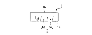
本実施形態に係るモールド(インプリント用型部材)1は、図1から図3に示すように、表面に基板用レジスト(基板用光硬化性樹脂)2が配設された基板3を押圧して、パターン面(一表面)1aに形成された凹部5Aと凸部5Bとからなるパターン5を基板3に転写するものであって、凹部5Aが、パターン面1aから深さ方向に漸次拡開して設けられている。図1に示すように、凹部5Aの角度θは、70度以上90度未満の所定の角度となっている。
An embodiment according to the present invention will be described with reference to FIGS.
As shown in FIGS. 1 to 3, the mold (imprint mold member) 1 according to this embodiment presses a
モールド1は、石英、ガラス、パイレックス(登録商標)といったSiO2を含むものや、サファイアを含む透明部材からなるモールド基板(型部材作製用素材)6から構成されている。
The
次に、本実施形態に係るモールド1の製造方法について説明する。
モールド1の製造方法は、モールド基板6に型用レジスト(型用光硬化性樹脂)7を塗布する工程と、露光、現像してモールド基板6のパターン面1aにパターン5を形成する工程と、凹部5Aの深さと幅とのアスペクト比、及び基板用レジスト2の体積収縮率から凹部5Aの傾斜角度を決める工程と、パターン面1aから深さ方向に漸次拡開した凹部5Aを形成するドライエッチング工程とを備えている。以下、各工程について詳述する。
Next, a method for manufacturing the
The method for manufacturing the
モールド基板6に型用レジスト7を塗布する工程では、まず、モールド基板6として例えば6インチの水晶基板を準備し、例えばZEP520(日本ゼオン株式会社製)といった型用レジスト7を500nmの厚さで表面に塗布する。 In the step of applying the mold resist 7 to the mold substrate 6, first, for example, a 6-inch quartz substrate is prepared as the mold substrate 6, and the mold resist 7 such as ZEP520 (manufactured by Nippon Zeon Co., Ltd.) is formed with a thickness of 500 nm. Apply to the surface.
露光、現像してモールド基板6のパターン面1aにパターン5を形成する工程では、図示しない電子線描画装置によって、図2(a)に示すように、型用レジスト7に対して100nm〜400nmのラインパターンを描画し、かつ有機現像して、図2(b)に示すようにパターン5を形成する。このときの条件は、例えば、描画時のドーズを100μC/cm2、現像時間を2分とする。
In the step of forming the
凹部5Aの傾斜角度を決める工程では、基板用レジスト2の収縮に係る有限要素法シミュレーションや実験データを元に角度θを決定する。インプリントに用いられる基板用レジスト2は3%〜20%の硬化収縮率を持っていることが分かっており、例えば体積収縮率14%とした場合、図3に示すような硬化収縮シミュレーション結果となる。
In the step of determining the inclination angle of the
こうして得られた収縮シミュレーション結果に基づいた傾斜角度を実現するために、例えば図示しないICPドライエッチング装置を用いてドライエッチング工程を行う。このときの条件は、例えば、CF4の流量を30cm3/s(30sccm)、O2の流量を30cm3/s(30sccm)、Arの流量を50cm3/s(50sccm)、圧力を2Pa、ICPパワーを500W、RIEパワーを500Wとする。 In order to realize an inclination angle based on the shrinkage simulation result obtained in this way, for example, a dry etching process is performed using an ICP dry etching apparatus (not shown). The conditions at this time are, for example, a flow rate of CF 4 of 30 cm 3 / s (30 sccm), a flow rate of O 2 of 30 cm 3 / s (30 sccm), a flow rate of Ar of 50 cm 3 / s (50 sccm), a pressure of 2 Pa, The ICP power is 500 W and the RIE power is 500 W.
そして、O2プラズマアッシングによって、型用レジスト7を基板3から剥離する。このときの条件は、例えば、O2の流量を500cm3/s(500sccm)、圧力30Pa、RFパワーを1000Wとする。
Then, the mold resist 7 is peeled from the
次に、こうして得られたモールド1を用いて基板3上に転写パターン8を形成するインプリント方法について説明する。
まず、図4(a)に示すモールド1のパターン面1aに離型剤として図示しないフッ素系表面処理剤EGC−1720(住友スリーエム株式会社製)を浸漬処理しておく。ここで、インプリントの対象となる基板3として、4インチシリコン基板を使用し、図4(b)に示すように、基板3上にラジカル重合型の基板用レジスト2を、例えば350nm厚で塗布する。
Next, an imprint method for forming the transfer pattern 8 on the
First, a fluorinated surface treating agent EGC-1720 (manufactured by Sumitomo 3M Co., Ltd.) (not shown) is immersed in the
そして、モールド1を上側、基板3を下側として、モールド1のパターン面1aと基板3とを対向させ、例えば、プレス圧力0.5Mpaにて、図4(c)に示すように、基板用レジスト2を加圧する。このとき、押圧された基板用レジスト2が凹部5A内に圧入される。このとき、基板用レジスト2は、凹部5Aの形状に合わせて基板3側からモールド1側に向かって漸次拡開して立設した状態となる。
Then, with the
この押圧状態を維持しながら、例えば、露光量1000mJ/cm2にてモールド1の裏面1bから露光して基板用レジスト2を硬化させる。このときの保持時間は1分とする。この際、図4(d)に示すように、凹部5A内の基板用レジスト2の先端側が基板3側よりも収縮して硬化するので、基板3に対して垂直方向に同一断面積に立設された状態となる。こうして、モールド1を離型することにより、図4(e)に示すような転写パターン8が基板3に形成される。
While maintaining this pressed state, for example, the substrate resist 2 is cured by exposure from the
このモールド1によれば、基板用レジスト2が配設された基板3にモールド1のパターン面1aを押圧したときに、凹部5A内に圧入された基板3上の基板用レジスト2を、基板3側からモールド1の内部に向かって漸次拡開するように立設させることができる。この際、基板用レジスト2を硬化させることによって、基板用レジスト2の先端側が基板3側よりも収縮するので、硬化した基板用レジスト2を最終的に垂直方向に立設させることができ、基板3上に垂直形状に立設された転写パターン8を得ることができる。
According to this
また、モールド基板6が透明部材からなるので、インプリントの際、モールド1の裏面1bから露光して基板3上の基板用レジスト2を硬化させることができる。
Since the mold substrate 6 is made of a transparent member, the substrate resist 2 on the
さらに、このモールド1の製造方法によれば、凹部5Aの深さと幅とのアスペクト比、及び基板用レジスト2の体積収縮率から凹部5Aの傾斜角度を決める工程を備えているので、基板3上の基板用レジスト2を硬化収縮後に垂直方向に立設させることができる。
Further, according to the method for manufacturing the
また、ドライエッチングにより凹部5Aを形成する工程を備えているので、モールド基板6に対して、所望の傾斜角度でパターン面1aから深さ方向に漸次拡開する凹部5Aを高精度に加工することができる。
Further, since the step of forming the
また、このモールド1を用いたインプリント方法によれば、基板3上に垂直形状に立設された転写パターン8を得ることができる。
Further, according to the imprint method using this
なお、本発明の技術範囲は上記実施の形態に限定されるものではなく、本発明の趣旨を逸脱しない範囲において種々の変更を加えることが可能である。
例えば、上記実施形態では、モールド1を製造する際に、ドライエッチング工程によって凹部5Aを形成しているが、代わりに、図5に示すように、垂直形状の原凹部10が形成されたモールド基板11に対して、深さ方向に漸次拡開するように収束イオンビーム12を用いて上述の形状の凹部5Aを形成してもよい。
The technical scope of the present invention is not limited to the above embodiment, and various modifications can be made without departing from the spirit of the present invention.
For example, in the above embodiment, when the
この場合、所望の傾斜角度にモールド基板11を保持し、加速電圧5kV〜50kV、電流値5nA〜30nAの収束イオンビーム(FIB)を照射して加工する。
In this case, the
又は、型用レジスト7によるリソグラフィによらずに、平面状のガラス基板に対して収束イオンビームを照射して、上述した形状の凹部5Aを直接加工してもよい。
Alternatively, the
また、ドライエッチング工程にて使用するドライエッチング装置は、ICP型ドライエッチング装置に限らず、RIE型ドライエッチング装置、ECR型ドライエッチング装置、マイクロ波型ドライエッチング装置、並行平板型ドライエッチング装置、ヘリコン派型ドライエッチング装置等、プラズマ発生方法に依存せず、任意のドライエッチング装置を使用しても構わない。 Also, the dry etching apparatus used in the dry etching process is not limited to the ICP type dry etching apparatus, but is also an RIE type dry etching apparatus, an ECR type dry etching apparatus, a microwave type dry etching apparatus, a parallel plate type dry etching apparatus, and a helicon. Any dry etching apparatus may be used without depending on the plasma generation method, such as a small dry etching apparatus.
1 モールド(インプリント用型部材)
1a パターン面(一表面)
2 基板用レジスト(基板用光硬化性樹脂)
3 基板
5 パターン
6,11 モールド基板(型部材作製用素材)
7 型用レジスト(型用光硬化性樹脂)
8 転写パターン
1 Mold (mold material for imprint)
1a Pattern surface (one surface)
2 Substrate resist (photocurable resin for substrates)
3
7 Resist for mold (photo-curable resin for mold)
8 Transfer patterns
Claims (6)
前記凹部が、前記一表面から深さ方向に漸次拡開して設けられていることを特徴とするインプリント用型部材。 An imprint mold member for pressing a substrate on which a photocurable resin for a substrate is disposed on a surface and transferring a pattern composed of a concave portion and a convex portion formed on one surface to the substrate,
The imprint mold member, wherein the concave portion is provided so as to gradually expand in the depth direction from the one surface.
前記型用光硬化性樹脂を硬化させた後、ドライエッチングによって前記インプリント用型部材の前記一表面から深さ方向に漸次拡開した凹部を形成する工程を備えていることを特徴とするインプリント用型部材の製造方法。 A method of manufacturing an imprint mold member for pressing a substrate surface on which a photocurable resin for a substrate is disposed and transferring a pattern formed of a concave portion and a convex portion formed on one surface,
And a step of forming a recess gradually expanding in the depth direction from the one surface of the imprint mold member by dry etching after curing the photocurable resin for the mold. A method for producing a printing mold member.
収束イオンビームを用いて前記インプリント用型部材の前記一表面から深さ方向に漸次拡開した凹部を形成する工程を備えていることを特徴とするインプリント用型部材の製造方法。 A method of manufacturing an imprint mold member for pressing a substrate surface on which a photocurable resin for a substrate is disposed and transferring a pattern formed of a concave portion and a convex portion formed on one surface,
The manufacturing method of the imprint mold member characterized by including the process of forming the recessed part gradually expanded in the depth direction from the said one surface of the said imprint mold member using a focused ion beam.
The imprint mold member according to claim 1 or 2, wherein the one surface of the imprint mold member is pressed against the substrate coated with the photocurable resin for a substrate and deformed to form a transfer pattern on the substrate. How to imprint.
Priority Applications (1)
| Application Number | Priority Date | Filing Date | Title |
|---|---|---|---|
| JP2006084347A JP4867423B2 (en) | 2006-03-27 | 2006-03-27 | Imprint mold member, imprint mold member manufacturing method, and imprint method |
Applications Claiming Priority (1)
| Application Number | Priority Date | Filing Date | Title |
|---|---|---|---|
| JP2006084347A JP4867423B2 (en) | 2006-03-27 | 2006-03-27 | Imprint mold member, imprint mold member manufacturing method, and imprint method |
Publications (2)
| Publication Number | Publication Date |
|---|---|
| JP2007253577A true JP2007253577A (en) | 2007-10-04 |
| JP4867423B2 JP4867423B2 (en) | 2012-02-01 |
Family
ID=38628280
Family Applications (1)
| Application Number | Title | Priority Date | Filing Date |
|---|---|---|---|
| JP2006084347A Expired - Fee Related JP4867423B2 (en) | 2006-03-27 | 2006-03-27 | Imprint mold member, imprint mold member manufacturing method, and imprint method |
Country Status (1)
| Country | Link |
|---|---|
| JP (1) | JP4867423B2 (en) |
Cited By (8)
| Publication number | Priority date | Publication date | Assignee | Title |
|---|---|---|---|---|
| JP2009226762A (en) * | 2008-03-24 | 2009-10-08 | Toppan Printing Co Ltd | Imprint mold, imprint mold manufacturing method and fine structural body |
| JP2010194733A (en) * | 2009-02-23 | 2010-09-09 | Toppan Printing Co Ltd | Method for producing mold for nano-imprints |
| WO2011033584A1 (en) * | 2009-09-18 | 2011-03-24 | 株式会社 東芝 | Mold |
| JP2011187824A (en) * | 2010-03-10 | 2011-09-22 | Fujifilm Corp | Fine pattern manufacturing method, substrate with fine pattern, and light source device and image display device including substrate with fine pattern |
| JP2012019019A (en) * | 2010-07-07 | 2012-01-26 | Toshiba Corp | Method for manufacturing template and method for manufacturing semiconductor device |
| KR101233096B1 (en) | 2009-06-26 | 2013-02-14 | 한국과학기술원 | Method for transferring pattern |
| WO2019160095A1 (en) * | 2018-02-19 | 2019-08-22 | 株式会社ダイセル | Mold manufacturing method |
| CN112599478A (en) * | 2021-01-15 | 2021-04-02 | 苏州芯聚半导体有限公司 | Driving substrate, manufacturing method and display panel |
Citations (3)
| Publication number | Priority date | Publication date | Assignee | Title |
|---|---|---|---|---|
| JPH1050576A (en) * | 1996-07-31 | 1998-02-20 | Sumitomo Electric Ind Ltd | Manufacture of mold for manufacturing microstructure and manufacture of microstructure |
| JP2006082476A (en) * | 2004-09-17 | 2006-03-30 | Seiko Instruments Inc | Mold manufacturing method and part manufactured using mold |
| JP2006137092A (en) * | 2004-11-12 | 2006-06-01 | Sumitomo Electric Ind Ltd | Method for producing minute mold, minute mold and minute structure produced by the method |
-
2006
- 2006-03-27 JP JP2006084347A patent/JP4867423B2/en not_active Expired - Fee Related
Patent Citations (3)
| Publication number | Priority date | Publication date | Assignee | Title |
|---|---|---|---|---|
| JPH1050576A (en) * | 1996-07-31 | 1998-02-20 | Sumitomo Electric Ind Ltd | Manufacture of mold for manufacturing microstructure and manufacture of microstructure |
| JP2006082476A (en) * | 2004-09-17 | 2006-03-30 | Seiko Instruments Inc | Mold manufacturing method and part manufactured using mold |
| JP2006137092A (en) * | 2004-11-12 | 2006-06-01 | Sumitomo Electric Ind Ltd | Method for producing minute mold, minute mold and minute structure produced by the method |
Cited By (11)
| Publication number | Priority date | Publication date | Assignee | Title |
|---|---|---|---|---|
| JP2009226762A (en) * | 2008-03-24 | 2009-10-08 | Toppan Printing Co Ltd | Imprint mold, imprint mold manufacturing method and fine structural body |
| JP2010194733A (en) * | 2009-02-23 | 2010-09-09 | Toppan Printing Co Ltd | Method for producing mold for nano-imprints |
| KR101233096B1 (en) | 2009-06-26 | 2013-02-14 | 한국과학기술원 | Method for transferring pattern |
| WO2011033584A1 (en) * | 2009-09-18 | 2011-03-24 | 株式会社 東芝 | Mold |
| JPWO2011033584A1 (en) * | 2009-09-18 | 2013-02-07 | 株式会社東芝 | mold |
| US8419412B2 (en) | 2009-09-18 | 2013-04-16 | Kabushiki Kaisha Toshiba | Nano-imprint mold and substrate with uneven patterns manufactured by using the mold |
| JP5421380B2 (en) * | 2009-09-18 | 2014-02-19 | 株式会社東芝 | mold |
| JP2011187824A (en) * | 2010-03-10 | 2011-09-22 | Fujifilm Corp | Fine pattern manufacturing method, substrate with fine pattern, and light source device and image display device including substrate with fine pattern |
| JP2012019019A (en) * | 2010-07-07 | 2012-01-26 | Toshiba Corp | Method for manufacturing template and method for manufacturing semiconductor device |
| WO2019160095A1 (en) * | 2018-02-19 | 2019-08-22 | 株式会社ダイセル | Mold manufacturing method |
| CN112599478A (en) * | 2021-01-15 | 2021-04-02 | 苏州芯聚半导体有限公司 | Driving substrate, manufacturing method and display panel |
Also Published As
| Publication number | Publication date |
|---|---|
| JP4867423B2 (en) | 2012-02-01 |
Similar Documents
| Publication | Publication Date | Title |
|---|---|---|
| JP5119579B2 (en) | Imprint mold and manufacturing method thereof | |
| JP4867423B2 (en) | Imprint mold member, imprint mold member manufacturing method, and imprint method | |
| US7922960B2 (en) | Fine resist pattern forming method and nanoimprint mold structure | |
| JP4940784B2 (en) | Imprint mold and imprint mold manufacturing method | |
| JP2008078550A (en) | Imprint mold, its manufacturing method, and pattern formation method | |
| JP2007027361A (en) | Mold for imprint | |
| JP2007266384A (en) | Mold for imprinting and manufacturing method thereof | |
| JP2013175671A (en) | Method for manufacturing replica template for nano-imprint and replica template | |
| JP4935312B2 (en) | Imprint mold and imprint mold manufacturing method | |
| JP2008132722A (en) | Mold for nano-imprinting, its fabricating method and method of manufacturing device using this mold | |
| JP5125655B2 (en) | Imprint mold | |
| JP2007103914A (en) | Mold, imprint device, and method of manufacturing device | |
| JP5114962B2 (en) | Imprint mold, imprint evaluation apparatus using the same, resist pattern forming method, and imprint mold manufacturing method | |
| JP2008200997A (en) | Method for manufacturing mold for nano-imprint | |
| JP2008119870A (en) | Imprinting mold | |
| JP2007210275A (en) | Mold for imprint | |
| JP6277588B2 (en) | Pattern forming method and nanoimprint template manufacturing method | |
| JP2011014875A (en) | Method for manufacturing structure | |
| JP2011014875A5 (en) | ||
| JP2007035998A (en) | Mold for imprint | |
| JP5211505B2 (en) | Imprint mold, imprint mold manufacturing method, and optical imprint method | |
| JP5326192B2 (en) | Imprint mold and imprint mold manufacturing method | |
| JP7178277B2 (en) | Imprint mold manufacturing method | |
| JP4858030B2 (en) | Imprint mold, imprint mold manufacturing method, and pattern forming method | |
| JP2011199136A (en) | Mold for imprint, method of fabricating the same, and pattern transferred body |
Legal Events
| Date | Code | Title | Description |
|---|---|---|---|
| A621 | Written request for application examination |
Free format text: JAPANESE INTERMEDIATE CODE: A621 Effective date: 20090223 |
|
| A977 | Report on retrieval |
Free format text: JAPANESE INTERMEDIATE CODE: A971007 Effective date: 20110715 |
|
| A131 | Notification of reasons for refusal |
Free format text: JAPANESE INTERMEDIATE CODE: A131 Effective date: 20110726 |
|
| A521 | Written amendment |
Free format text: JAPANESE INTERMEDIATE CODE: A523 Effective date: 20110921 |
|
| TRDD | Decision of grant or rejection written | ||
| A01 | Written decision to grant a patent or to grant a registration (utility model) |
Free format text: JAPANESE INTERMEDIATE CODE: A01 Effective date: 20111018 |
|
| A01 | Written decision to grant a patent or to grant a registration (utility model) |
Free format text: JAPANESE INTERMEDIATE CODE: A01 |
|
| A61 | First payment of annual fees (during grant procedure) |
Free format text: JAPANESE INTERMEDIATE CODE: A61 Effective date: 20111031 |
|
| R150 | Certificate of patent or registration of utility model |
Free format text: JAPANESE INTERMEDIATE CODE: R150 |
|
| FPAY | Renewal fee payment (event date is renewal date of database) |
Free format text: PAYMENT UNTIL: 20141125 Year of fee payment: 3 |
|
| LAPS | Cancellation because of no payment of annual fees |