JP5974429B2 - 複合材料構造物及びその製造方法 - Google Patents
複合材料構造物及びその製造方法 Download PDFInfo
- Publication number
- JP5974429B2 JP5974429B2 JP2011158723A JP2011158723A JP5974429B2 JP 5974429 B2 JP5974429 B2 JP 5974429B2 JP 2011158723 A JP2011158723 A JP 2011158723A JP 2011158723 A JP2011158723 A JP 2011158723A JP 5974429 B2 JP5974429 B2 JP 5974429B2
- Authority
- JP
- Japan
- Prior art keywords
- space
- flow path
- base material
- liquid
- microchip
- Prior art date
- Legal status (The legal status is an assumption and is not a legal conclusion. Google has not performed a legal analysis and makes no representation as to the accuracy of the status listed.)
- Active
Links
Images


Classifications
-
- B—PERFORMING OPERATIONS; TRANSPORTING
- B32—LAYERED PRODUCTS
- B32B—LAYERED PRODUCTS, i.e. PRODUCTS BUILT-UP OF STRATA OF FLAT OR NON-FLAT, e.g. CELLULAR OR HONEYCOMB, FORM
- B32B3/00—Layered products comprising a layer with external or internal discontinuities or unevennesses, or a layer of non-planar form; Layered products having particular features of form
- B32B3/26—Layered products comprising a layer with external or internal discontinuities or unevennesses, or a layer of non-planar form; Layered products having particular features of form characterised by a particular shape of the outline of the cross-section of a continuous layer; characterised by a layer with cavities or internal voids ; characterised by an apertured layer
- B32B3/30—Layered products comprising a layer with external or internal discontinuities or unevennesses, or a layer of non-planar form; Layered products having particular features of form characterised by a particular shape of the outline of the cross-section of a continuous layer; characterised by a layer with cavities or internal voids ; characterised by an apertured layer characterised by a layer formed with recesses or projections, e.g. hollows, grooves, protuberances, ribs
-
- B—PERFORMING OPERATIONS; TRANSPORTING
- B01—PHYSICAL OR CHEMICAL PROCESSES OR APPARATUS IN GENERAL
- B01L—CHEMICAL OR PHYSICAL LABORATORY APPARATUS FOR GENERAL USE
- B01L3/00—Containers or dishes for laboratory use, e.g. laboratory glassware; Droppers
- B01L3/50—Containers for the purpose of retaining a material to be analysed, e.g. test tubes
- B01L3/502—Containers for the purpose of retaining a material to be analysed, e.g. test tubes with fluid transport, e.g. in multi-compartment structures
- B01L3/5027—Containers for the purpose of retaining a material to be analysed, e.g. test tubes with fluid transport, e.g. in multi-compartment structures by integrated microfluidic structures, i.e. dimensions of channels and chambers are such that surface tension forces are important, e.g. lab-on-a-chip
- B01L3/502707—Containers for the purpose of retaining a material to be analysed, e.g. test tubes with fluid transport, e.g. in multi-compartment structures by integrated microfluidic structures, i.e. dimensions of channels and chambers are such that surface tension forces are important, e.g. lab-on-a-chip characterised by the manufacture of the container or its components
-
- B—PERFORMING OPERATIONS; TRANSPORTING
- B01—PHYSICAL OR CHEMICAL PROCESSES OR APPARATUS IN GENERAL
- B01L—CHEMICAL OR PHYSICAL LABORATORY APPARATUS FOR GENERAL USE
- B01L3/00—Containers or dishes for laboratory use, e.g. laboratory glassware; Droppers
- B01L3/50—Containers for the purpose of retaining a material to be analysed, e.g. test tubes
- B01L3/502—Containers for the purpose of retaining a material to be analysed, e.g. test tubes with fluid transport, e.g. in multi-compartment structures
- B01L3/5027—Containers for the purpose of retaining a material to be analysed, e.g. test tubes with fluid transport, e.g. in multi-compartment structures by integrated microfluidic structures, i.e. dimensions of channels and chambers are such that surface tension forces are important, e.g. lab-on-a-chip
- B01L3/502715—Containers for the purpose of retaining a material to be analysed, e.g. test tubes with fluid transport, e.g. in multi-compartment structures by integrated microfluidic structures, i.e. dimensions of channels and chambers are such that surface tension forces are important, e.g. lab-on-a-chip characterised by interfacing components, e.g. fluidic, electrical, optical or mechanical interfaces
-
- B—PERFORMING OPERATIONS; TRANSPORTING
- B32—LAYERED PRODUCTS
- B32B—LAYERED PRODUCTS, i.e. PRODUCTS BUILT-UP OF STRATA OF FLAT OR NON-FLAT, e.g. CELLULAR OR HONEYCOMB, FORM
- B32B27/00—Layered products comprising a layer of synthetic resin
- B32B27/06—Layered products comprising a layer of synthetic resin as the main or only constituent of a layer, which is next to another layer of the same or of a different material
- B32B27/08—Layered products comprising a layer of synthetic resin as the main or only constituent of a layer, which is next to another layer of the same or of a different material of synthetic resin
-
- B—PERFORMING OPERATIONS; TRANSPORTING
- B32—LAYERED PRODUCTS
- B32B—LAYERED PRODUCTS, i.e. PRODUCTS BUILT-UP OF STRATA OF FLAT OR NON-FLAT, e.g. CELLULAR OR HONEYCOMB, FORM
- B32B3/00—Layered products comprising a layer with external or internal discontinuities or unevennesses, or a layer of non-planar form; Layered products having particular features of form
- B32B3/02—Layered products comprising a layer with external or internal discontinuities or unevennesses, or a layer of non-planar form; Layered products having particular features of form characterised by features of form at particular places, e.g. in edge regions
- B32B3/08—Layered products comprising a layer with external or internal discontinuities or unevennesses, or a layer of non-planar form; Layered products having particular features of form characterised by features of form at particular places, e.g. in edge regions characterised by added members at particular parts
-
- B—PERFORMING OPERATIONS; TRANSPORTING
- B32—LAYERED PRODUCTS
- B32B—LAYERED PRODUCTS, i.e. PRODUCTS BUILT-UP OF STRATA OF FLAT OR NON-FLAT, e.g. CELLULAR OR HONEYCOMB, FORM
- B32B3/00—Layered products comprising a layer with external or internal discontinuities or unevennesses, or a layer of non-planar form; Layered products having particular features of form
- B32B3/26—Layered products comprising a layer with external or internal discontinuities or unevennesses, or a layer of non-planar form; Layered products having particular features of form characterised by a particular shape of the outline of the cross-section of a continuous layer; characterised by a layer with cavities or internal voids ; characterised by an apertured layer
- B32B3/266—Layered products comprising a layer with external or internal discontinuities or unevennesses, or a layer of non-planar form; Layered products having particular features of form characterised by a particular shape of the outline of the cross-section of a continuous layer; characterised by a layer with cavities or internal voids ; characterised by an apertured layer characterised by an apertured layer, the apertures going through the whole thickness of the layer, e.g. expanded metal, perforated layer, slit layer regular cells B32B3/12
-
- G—PHYSICS
- G01—MEASURING; TESTING
- G01N—INVESTIGATING OR ANALYSING MATERIALS BY DETERMINING THEIR CHEMICAL OR PHYSICAL PROPERTIES
- G01N21/00—Investigating or analysing materials by the use of optical means, i.e. using sub-millimetre waves, infrared, visible or ultraviolet light
- G01N21/17—Systems in which incident light is modified in accordance with the properties of the material investigated
- G01N21/47—Scattering, i.e. diffuse reflection
- G01N21/49—Scattering, i.e. diffuse reflection within a body or fluid
- G01N21/51—Scattering, i.e. diffuse reflection within a body or fluid inside a container, e.g. in an ampoule
-
- B—PERFORMING OPERATIONS; TRANSPORTING
- B01—PHYSICAL OR CHEMICAL PROCESSES OR APPARATUS IN GENERAL
- B01L—CHEMICAL OR PHYSICAL LABORATORY APPARATUS FOR GENERAL USE
- B01L2200/00—Solutions for specific problems relating to chemical or physical laboratory apparatus
- B01L2200/06—Fluid handling related problems
- B01L2200/0636—Focussing flows, e.g. to laminate flows
-
- B—PERFORMING OPERATIONS; TRANSPORTING
- B01—PHYSICAL OR CHEMICAL PROCESSES OR APPARATUS IN GENERAL
- B01L—CHEMICAL OR PHYSICAL LABORATORY APPARATUS FOR GENERAL USE
- B01L2200/00—Solutions for specific problems relating to chemical or physical laboratory apparatus
- B01L2200/06—Fluid handling related problems
- B01L2200/0689—Sealing
-
- B—PERFORMING OPERATIONS; TRANSPORTING
- B01—PHYSICAL OR CHEMICAL PROCESSES OR APPARATUS IN GENERAL
- B01L—CHEMICAL OR PHYSICAL LABORATORY APPARATUS FOR GENERAL USE
- B01L2200/00—Solutions for specific problems relating to chemical or physical laboratory apparatus
- B01L2200/12—Specific details about manufacturing devices
-
- B—PERFORMING OPERATIONS; TRANSPORTING
- B01—PHYSICAL OR CHEMICAL PROCESSES OR APPARATUS IN GENERAL
- B01L—CHEMICAL OR PHYSICAL LABORATORY APPARATUS FOR GENERAL USE
- B01L2300/00—Additional constructional details
- B01L2300/06—Auxiliary integrated devices, integrated components
- B01L2300/0627—Sensor or part of a sensor is integrated
- B01L2300/0645—Electrodes
-
- B—PERFORMING OPERATIONS; TRANSPORTING
- B01—PHYSICAL OR CHEMICAL PROCESSES OR APPARATUS IN GENERAL
- B01L—CHEMICAL OR PHYSICAL LABORATORY APPARATUS FOR GENERAL USE
- B01L2300/00—Additional constructional details
- B01L2300/06—Auxiliary integrated devices, integrated components
- B01L2300/0627—Sensor or part of a sensor is integrated
- B01L2300/0654—Lenses; Optical fibres
-
- B—PERFORMING OPERATIONS; TRANSPORTING
- B01—PHYSICAL OR CHEMICAL PROCESSES OR APPARATUS IN GENERAL
- B01L—CHEMICAL OR PHYSICAL LABORATORY APPARATUS FOR GENERAL USE
- B01L2300/00—Additional constructional details
- B01L2300/08—Geometry, shape and general structure
- B01L2300/0809—Geometry, shape and general structure rectangular shaped
- B01L2300/0816—Cards, e.g. flat sample carriers usually with flow in two horizontal directions
-
- B—PERFORMING OPERATIONS; TRANSPORTING
- B01—PHYSICAL OR CHEMICAL PROCESSES OR APPARATUS IN GENERAL
- B01L—CHEMICAL OR PHYSICAL LABORATORY APPARATUS FOR GENERAL USE
- B01L2300/00—Additional constructional details
- B01L2300/08—Geometry, shape and general structure
- B01L2300/0832—Geometry, shape and general structure cylindrical, tube shaped
- B01L2300/0838—Capillaries
-
- B—PERFORMING OPERATIONS; TRANSPORTING
- B01—PHYSICAL OR CHEMICAL PROCESSES OR APPARATUS IN GENERAL
- B01L—CHEMICAL OR PHYSICAL LABORATORY APPARATUS FOR GENERAL USE
- B01L2300/00—Additional constructional details
- B01L2300/08—Geometry, shape and general structure
- B01L2300/0861—Configuration of multiple channels and/or chambers in a single devices
- B01L2300/0877—Flow chambers
-
- B—PERFORMING OPERATIONS; TRANSPORTING
- B01—PHYSICAL OR CHEMICAL PROCESSES OR APPARATUS IN GENERAL
- B01L—CHEMICAL OR PHYSICAL LABORATORY APPARATUS FOR GENERAL USE
- B01L2300/00—Additional constructional details
- B01L2300/08—Geometry, shape and general structure
- B01L2300/0887—Laminated structure
-
- B—PERFORMING OPERATIONS; TRANSPORTING
- B32—LAYERED PRODUCTS
- B32B—LAYERED PRODUCTS, i.e. PRODUCTS BUILT-UP OF STRATA OF FLAT OR NON-FLAT, e.g. CELLULAR OR HONEYCOMB, FORM
- B32B2307/00—Properties of the layers or laminate
- B32B2307/40—Properties of the layers or laminate having particular optical properties
- B32B2307/412—Transparent
-
- G—PHYSICS
- G01—MEASURING; TESTING
- G01N—INVESTIGATING OR ANALYSING MATERIALS BY DETERMINING THEIR CHEMICAL OR PHYSICAL PROPERTIES
- G01N21/00—Investigating or analysing materials by the use of optical means, i.e. using sub-millimetre waves, infrared, visible or ultraviolet light
- G01N21/17—Systems in which incident light is modified in accordance with the properties of the material investigated
- G01N21/47—Scattering, i.e. diffuse reflection
- G01N21/49—Scattering, i.e. diffuse reflection within a body or fluid
- G01N21/51—Scattering, i.e. diffuse reflection within a body or fluid inside a container, e.g. in an ampoule
- G01N2021/513—Cuvettes for scattering measurements
-
- G—PHYSICS
- G01—MEASURING; TESTING
- G01N—INVESTIGATING OR ANALYSING MATERIALS BY DETERMINING THEIR CHEMICAL OR PHYSICAL PROPERTIES
- G01N21/00—Investigating or analysing materials by the use of optical means, i.e. using sub-millimetre waves, infrared, visible or ultraviolet light
- G01N21/62—Systems in which the material investigated is excited whereby it emits light or causes a change in wavelength of the incident light
- G01N21/63—Systems in which the material investigated is excited whereby it emits light or causes a change in wavelength of the incident light optically excited
- G01N21/64—Fluorescence; Phosphorescence
- G01N21/645—Specially adapted constructive features of fluorimeters
- G01N2021/6482—Sample cells, cuvettes
-
- G—PHYSICS
- G01—MEASURING; TESTING
- G01N—INVESTIGATING OR ANALYSING MATERIALS BY DETERMINING THEIR CHEMICAL OR PHYSICAL PROPERTIES
- G01N21/00—Investigating or analysing materials by the use of optical means, i.e. using sub-millimetre waves, infrared, visible or ultraviolet light
- G01N21/62—Systems in which the material investigated is excited whereby it emits light or causes a change in wavelength of the incident light
- G01N21/63—Systems in which the material investigated is excited whereby it emits light or causes a change in wavelength of the incident light optically excited
- G01N21/64—Fluorescence; Phosphorescence
- G01N21/645—Specially adapted constructive features of fluorimeters
-
- G—PHYSICS
- G01—MEASURING; TESTING
- G01N—INVESTIGATING OR ANALYSING MATERIALS BY DETERMINING THEIR CHEMICAL OR PHYSICAL PROPERTIES
- G01N2201/00—Features of devices classified in G01N21/00
- G01N2201/06—Illumination; Optics
- G01N2201/061—Sources
- G01N2201/06113—Coherent sources; lasers
-
- Y—GENERAL TAGGING OF NEW TECHNOLOGICAL DEVELOPMENTS; GENERAL TAGGING OF CROSS-SECTIONAL TECHNOLOGIES SPANNING OVER SEVERAL SECTIONS OF THE IPC; TECHNICAL SUBJECTS COVERED BY FORMER USPC CROSS-REFERENCE ART COLLECTIONS [XRACs] AND DIGESTS
- Y10—TECHNICAL SUBJECTS COVERED BY FORMER USPC
- Y10T—TECHNICAL SUBJECTS COVERED BY FORMER US CLASSIFICATION
- Y10T428/00—Stock material or miscellaneous articles
- Y10T428/24—Structurally defined web or sheet [e.g., overall dimension, etc.]
- Y10T428/24479—Structurally defined web or sheet [e.g., overall dimension, etc.] including variation in thickness
- Y10T428/24612—Composite web or sheet
Description
この複合材料構造物では、前記空間内における前記部材の位置を熱変形した前記壁面によって位置決めすることにより、前記基材の少なくとも一以上と前記部材とにそれぞれ形成された領域が連絡され繋ぎ合わされている。
この複合材料構造物は、前記領域として液体が通流される流路が形成されたマイクロチップとすることができ、さらに前記流路を通流する液体あるいは該液体に含まれる試料に対して光が照射される光照射部を備えるものとできる。この場合、前記光照射部は、前記基材を構成する前記熱可塑性樹脂よりも光透過性に優れた材料からなる部材によって構成することが好適となる。
この複合材料構造物の製造方法では、前記空間内における前記部材の位置を熱変形した前記壁面によって位置決めすることにより、前記基材の少なくとも一以上と前記部材とにそれぞれ形成された領域を連絡し繋ぎ合わせることができる。
この複合材料構造物の製造方法において、前記基材の熱圧着は、前記基材を構成する前記熱可塑性樹脂の熱変形温度よりも高く、かつ、前記部材を構成する材料の熱変形温度よりも低い温度で行われる。
1.複合材料構造物
2.複合材料構造物の製造方法
3.微小粒子分析用マイクロチップ
図1は、本技術に係る複合材料構造物の構成を説明する上面模式図である。また、図2及び図3は、本技術に係る複合材料構造物の構成を説明する断面模式図である。図2は図1中P−P断面に対応し、図3はQ−Q断面に対応する。
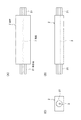
次に、図4〜図6を参照して、上述のマイクロチップAを例に、本技術に係る複合材料構造物の製造方法について説明する。図4は、基材11,12の構成を説明する断面模式図であり、図2において部材2を省略した図に相当する。図5は、部材2の構成を説明する模式図であり、(A)は上面図、(B)は側面図、(C)は正面図を示す。図6は、基材11,12と部材2の接合部の構成を説明する断面模式図であり、(A)は基材11,12の熱変形前、(B)は熱変形後を示す。なお、図6は、図1中Q−Q断面に対応している。
上述したマイクロチップAの具体的な実施形態の一例として、マイクロチップAを微小粒子分析のために用いる例を説明する。なお、微小粒子分析用のマイクロチップとしては、先に挙げた特許文献1を参照可能である。
(1)熱可塑性樹脂からなり、熱圧着により接合された二以上の基材と、前記熱可塑性樹脂よりも熱変形温度が高い材料からなり、前記基材の少なくとも一つに形成された空間内に挿入された一以上の部材と、から構成され、前記空間内に挿入された前記部材が、熱圧着により熱変形した前記基材の前記空間を構成する壁面によって固定保持されている複合材料構造物。
(2)前記空間内における前記部材の位置が前記壁面によって位置決めされている上記(1)記載の複合材料構造物。
(3)前記基材の少なくとも一以上と前記部材とにそれぞれ形成された領域が連絡するように、前記部材が前記空間内に位置決めされている上記(1)又は(2)記載の複合材料構造物。
(4)前記領域として液体が通流される流路が形成されたマイクロチップである上記(3)記載の複合材料構造物。
(5)前記流路を通流する液体あるいは該液体に含まれる試料に対して光が照射される光照射部を備え、前記基材を構成する前記熱可塑性樹脂よりも光透過性に優れた材料からなる前記部材によって、前記光照射部が構成されている上記(4)記載の複合材料構造物。
(1)熱可塑性樹脂からなり、少なくとも一つに形成された空間を有する二以上の基材を配する工程と、前記空間内に、前記熱可塑性樹脂よりも熱変形温度が高い材料からなる一以上の部材を挿入する工程と、前記基材を熱圧着により接合することによって、前記空間内に挿入された前記部材を、熱変形した前記基材の前記空間を構成する壁面によって固定保持させる工程と、を含む複合材料構造物の製造方法。
(2)前記固定保持させる工程において、前記空間内における前記部材の位置を前記壁面によって位置決めする上記(1)記載の製造方法。
(3)前記固定保持させる工程において、前記基材の少なくとも一以上と前記部材とにそれぞれ形成された領域が連絡するように、前記部材を前記空間内に位置決めする上記(1)又は(2)記載の製造方法。
(4)前記固定保持させる工程において、前記基材を構成する前記熱可塑性樹脂の熱変形温度よりも高く、かつ、前記部材を構成する材料の熱変形温度よりも低い温度で、前記基材の熱圧着を行う上記(1)〜(3)のいずれかに記載の製造方法。
Claims (10)
- 熱可塑性樹脂からなり、熱圧着により接合されている二以上の基材と、
前記熱可塑性樹脂よりも熱変形温度が高い材料からなり、前記基材の少なくとも一つが有する空間内に挿入されている一以上の部材と、から構成され、
前記基材のうち少なくとも一つと前記部材のそれぞれに液体が通流される流路が形成されており、
前記流路を通流する前記液体あるいは前記液体に含まれる試料に対して光が照射される光照射部を備え、
前記空間内に挿入されている前記部材が、熱圧着により熱変形した前記基材の前記空間を構成する壁面によって固定保持されているマイクロチップ。 - 前記空間内における前記部材の位置が前記壁面によって位置決めされている請求項1記載のマイクロチップ。
- 前記基材の少なくとも一つと前記部材とにそれぞれ形成された前記流路が連絡するように、前記部材が前記空間内に位置決めされている請求項1又は2記載のマイクロチップ。
- 前記光照射部は前記基材を構成する前記熱可塑性樹脂よりも光透過性に優れた材料からなる請求項1〜3のいずれか一項に記載のマイクロチップ。
- 前記基材の少なくとも一つに形成された前記流路は、微小粒子を含むサンプル液を導入するサンプルインレットと、前記微小粒子を含む液滴を排出する吐出口と、を備える請求項1〜4記載のマイクロチップ。
- 前記基材の少なくとも一つに形成された前記流路は、シース液を導入するシースインレットと、前記サンプル液及び前記シース液が合流する合流部と、を備える請求項5記載のマイクロチップ。
- 熱可塑性樹脂からなり、少なくとも一つに形成された空間を有する二以上の基材を配する工程と、
前記空間内に、前記熱可塑性樹脂よりも熱変形温度が高い材料からなる一以上の部材を挿入する工程と、
前記基材を熱圧着により接合することによって、前記空間内に挿入された前記部材を、熱変形した前記基材の前記空間を構成する壁面によって固定保持させる工程と、
を含み、
前記固定保持させる工程において、前記基材の少なくとも一以上と前記部材とにそれぞれ形成された流路が連絡するように、前記部材を前記空間内に位置決めするマイクロチップの製造方法。 - 前記流路を通流する液体あるいは該液体に含まれる試料に対して光が照射される光照射部を形成する工程と、を更に含む請求項7記載の製造方法。
- 前記固定保持させる工程において、前記空間内における前記部材の位置を前記壁面によって位置決めする請求項7又は8記載の製造方法。
- 前記固定保持させる工程において、前記基材を構成する前記熱可塑性樹脂の熱変形温度よりも高く、かつ、前記部材を構成する材料の熱変形温度よりも低い温度で、前記基材の熱圧着を行う請求項7〜9のいずれか一項に記載の製造方法。
Priority Applications (8)
| Application Number | Priority Date | Filing Date | Title |
|---|---|---|---|
| JP2011158723A JP5974429B2 (ja) | 2011-07-20 | 2011-07-20 | 複合材料構造物及びその製造方法 |
| CN201280034743.XA CN103702826B (zh) | 2011-07-20 | 2012-06-15 | 复合结构体及其制造方法 |
| CN201510420058.6A CN105126940B (zh) | 2011-07-20 | 2012-06-15 | 复合结构体和用于分析微粒子的微芯片 |
| IN261DEN2014 IN2014DN00261A (ja) | 2011-07-20 | 2012-06-15 | |
| PCT/JP2012/003939 WO2013011629A1 (en) | 2011-07-20 | 2012-06-15 | Composite structure and manufacturing method therefor |
| EP12731185.0A EP2734361B1 (en) | 2011-07-20 | 2012-06-15 | Composite structure and manufacturing method therefor |
| US14/131,730 US9610750B2 (en) | 2011-07-20 | 2012-06-15 | Composite structure and manufacturing method therefor |
| US15/444,906 US10414118B2 (en) | 2011-07-20 | 2017-02-28 | Microchip manufactured with thermocompression |
Applications Claiming Priority (1)
| Application Number | Priority Date | Filing Date | Title |
|---|---|---|---|
| JP2011158723A JP5974429B2 (ja) | 2011-07-20 | 2011-07-20 | 複合材料構造物及びその製造方法 |
Publications (3)
| Publication Number | Publication Date |
|---|---|
| JP2013022804A JP2013022804A (ja) | 2013-02-04 |
| JP2013022804A5 JP2013022804A5 (ja) | 2014-07-31 |
| JP5974429B2 true JP5974429B2 (ja) | 2016-08-23 |
Family
ID=46420487
Family Applications (1)
| Application Number | Title | Priority Date | Filing Date |
|---|---|---|---|
| JP2011158723A Active JP5974429B2 (ja) | 2011-07-20 | 2011-07-20 | 複合材料構造物及びその製造方法 |
Country Status (6)
| Country | Link |
|---|---|
| US (2) | US9610750B2 (ja) |
| EP (1) | EP2734361B1 (ja) |
| JP (1) | JP5974429B2 (ja) |
| CN (2) | CN103702826B (ja) |
| IN (1) | IN2014DN00261A (ja) |
| WO (1) | WO2013011629A1 (ja) |
Families Citing this family (2)
| Publication number | Priority date | Publication date | Assignee | Title |
|---|---|---|---|---|
| CN108393103A (zh) * | 2018-03-03 | 2018-08-14 | 北京工业大学 | 一种可实现液滴尺寸不依赖流量的微流控芯片 |
| US11665929B2 (en) * | 2019-06-13 | 2023-05-30 | Intel Corporation | Micro light-emitting diode displays with improved power efficiency |
Family Cites Families (22)
| Publication number | Priority date | Publication date | Assignee | Title |
|---|---|---|---|---|
| JPH0524516Y2 (ja) * | 1987-04-21 | 1993-06-22 | ||
| JPH03156888A (ja) * | 1989-08-28 | 1991-07-04 | Toshiba Corp | 分散型elパネル及びその製造方法 |
| GB8926294D0 (en) * | 1989-11-21 | 1990-01-10 | British Gas Plc | Method of jointing hollow members by fusion |
| US5427663A (en) | 1993-06-08 | 1995-06-27 | British Technology Group Usa Inc. | Microlithographic array for macromolecule and cell fractionation |
| GB9418981D0 (en) | 1994-09-21 | 1994-11-09 | Univ Glasgow | Apparatus and method for carrying out analysis of samples |
| JP3388392B2 (ja) * | 1999-06-02 | 2003-03-17 | 日精樹脂工業株式会社 | Icカード製造装置 |
| AU2002213043A1 (en) * | 2000-10-06 | 2002-04-15 | Protasis Corporation | Fluid separation conduit cartridge |
| US6564475B2 (en) * | 2000-12-22 | 2003-05-20 | K-Swiss Inc. | Footwear with enhanced temperature control |
| CN101158447B (zh) | 2002-12-04 | 2012-12-26 | 斯宾克斯公司 | 流体的可程控微量控制用装置和方法 |
| JP4074921B2 (ja) * | 2003-03-14 | 2008-04-16 | 日本電気株式会社 | 質量分析システムおよび分析方法 |
| JP4695851B2 (ja) * | 2003-07-10 | 2011-06-08 | シチズンホールディングス株式会社 | マイクロ化学チップ温度調節装置 |
| JP4304120B2 (ja) * | 2004-04-30 | 2009-07-29 | ベイバイオサイエンス株式会社 | 生物学的粒子をソーティングする装置及び方法 |
| CN1687766A (zh) | 2005-04-21 | 2005-10-26 | 复旦大学 | 一种纤维电泳芯片及其制备方法 |
| EP1893336A2 (en) * | 2005-05-19 | 2008-03-05 | Koninklijke Philips Electronics N.V. | Functional assembly and method of obtaining it |
| JP4695977B2 (ja) * | 2005-12-21 | 2011-06-08 | 東ソー・クォーツ株式会社 | マイクロチップ及びその製造方法 |
| JP2007263706A (ja) * | 2006-03-28 | 2007-10-11 | Aisin Seiki Co Ltd | バイオアッセイ用マイクロチップ |
| US8312646B2 (en) * | 2006-05-25 | 2012-11-20 | Nike, Inc. | Article of footwear incorporating a tensile element |
| EP1972909A1 (en) | 2007-03-23 | 2008-09-24 | Koninklijke Philips Electronics N.V. | Luminescence sensor |
| US7880108B2 (en) * | 2007-10-26 | 2011-02-01 | Becton, Dickinson And Company | Deflection plate |
| JP2009243965A (ja) * | 2008-03-28 | 2009-10-22 | Sumitomo Bakelite Co Ltd | 流路デバイス、外装ケース付き流路デバイス、流路デバイスの使用方法 |
| JP4572973B2 (ja) * | 2008-06-16 | 2010-11-04 | ソニー株式会社 | マイクロチップ及びマイクロチップにおける送流方法 |
| JP5487638B2 (ja) * | 2009-02-17 | 2014-05-07 | ソニー株式会社 | 微小粒子分取のための装置及びマイクロチップ |
-
2011
- 2011-07-20 JP JP2011158723A patent/JP5974429B2/ja active Active
-
2012
- 2012-06-15 EP EP12731185.0A patent/EP2734361B1/en not_active Not-in-force
- 2012-06-15 CN CN201280034743.XA patent/CN103702826B/zh active Active
- 2012-06-15 WO PCT/JP2012/003939 patent/WO2013011629A1/en active Application Filing
- 2012-06-15 CN CN201510420058.6A patent/CN105126940B/zh active Active
- 2012-06-15 IN IN261DEN2014 patent/IN2014DN00261A/en unknown
- 2012-06-15 US US14/131,730 patent/US9610750B2/en active Active
-
2017
- 2017-02-28 US US15/444,906 patent/US10414118B2/en active Active
Also Published As
| Publication number | Publication date |
|---|---|
| CN105126940A (zh) | 2015-12-09 |
| JP2013022804A (ja) | 2013-02-04 |
| US20140154475A1 (en) | 2014-06-05 |
| WO2013011629A1 (en) | 2013-01-24 |
| IN2014DN00261A (ja) | 2015-06-05 |
| CN105126940B (zh) | 2018-05-18 |
| US9610750B2 (en) | 2017-04-04 |
| US20170203296A1 (en) | 2017-07-20 |
| US10414118B2 (en) | 2019-09-17 |
| CN103702826A (zh) | 2014-04-02 |
| EP2734361A1 (en) | 2014-05-28 |
| EP2734361B1 (en) | 2017-08-09 |
| CN103702826B (zh) | 2015-08-19 |
Similar Documents
| Publication | Publication Date | Title |
|---|---|---|
| JP6003020B2 (ja) | マイクロチップ及び微小粒子分析装置 | |
| JP4661942B2 (ja) | マイクロチップとその流路構造 | |
| KR101850548B1 (ko) | 미소 입자 분류 장치, 마이크로칩 모듈 및 미소 입자들의 분류 방법 | |
| US8246805B2 (en) | Micro-fluidic chip and flow sending method in micro-fluidic chip | |
| EP2191895B1 (en) | Microparticle analysis device, microfluidic chip for microparticle analysis, and microparticle analysis method | |
| US20080213821A1 (en) | Microfluidic Cell Sorter System | |
| Shrirao et al. | Microfluidic flow cytometry: The role of microfabrication methodologies, performance and functional specification | |
| KR20130045236A (ko) | 마이크로칩 및 미립자 분석 장치 | |
| JP5974429B2 (ja) | 複合材料構造物及びその製造方法 | |
| JP5316530B2 (ja) | マイクロチップとその流路構造 | |
| CN107427831B (zh) | 微芯片、分析设备以及分析方法 | |
| JP5092881B2 (ja) | 流路構造及びマイクロチップ | |
| JP6965953B2 (ja) | マイクロチップ及び微小粒子分析装置 | |
| WO2021100618A1 (ja) | マイクロチップ、サンプル分取キット及び微小粒子分取装置 | |
| WO2022185980A1 (ja) | 粒子分取キット | |
| WO2019230489A1 (ja) | マイクロチップ及びサンプル分取キット | |
| JP2013250229A (ja) | 微小粒子分取用マイクロチップ、該微小粒子分取用マイクロチップが搭載された微小粒子分取装置、並びに微小粒子の分取方法 |
Legal Events
| Date | Code | Title | Description |
|---|---|---|---|
| A521 | Written amendment |
Free format text: JAPANESE INTERMEDIATE CODE: A523 Effective date: 20140617 |
|
| A621 | Written request for application examination |
Free format text: JAPANESE INTERMEDIATE CODE: A621 Effective date: 20140617 |
|
| A131 | Notification of reasons for refusal |
Free format text: JAPANESE INTERMEDIATE CODE: A131 Effective date: 20150901 |
|
| A521 | Written amendment |
Free format text: JAPANESE INTERMEDIATE CODE: A523 Effective date: 20151030 |
|
| A131 | Notification of reasons for refusal |
Free format text: JAPANESE INTERMEDIATE CODE: A131 Effective date: 20160308 |
|
| A521 | Written amendment |
Free format text: JAPANESE INTERMEDIATE CODE: A523 Effective date: 20160420 |
|
| TRDD | Decision of grant or rejection written | ||
| A01 | Written decision to grant a patent or to grant a registration (utility model) |
Free format text: JAPANESE INTERMEDIATE CODE: A01 Effective date: 20160621 |
|
| A61 | First payment of annual fees (during grant procedure) |
Free format text: JAPANESE INTERMEDIATE CODE: A61 Effective date: 20160704 |
|
| R151 | Written notification of patent or utility model registration |
Ref document number: 5974429 Country of ref document: JP Free format text: JAPANESE INTERMEDIATE CODE: R151 |
|
| R250 | Receipt of annual fees |
Free format text: JAPANESE INTERMEDIATE CODE: R250 |
|
| R250 | Receipt of annual fees |
Free format text: JAPANESE INTERMEDIATE CODE: R250 |