EP2734361B1 - Composite structure and manufacturing method therefor - Google Patents
Composite structure and manufacturing method therefor Download PDFInfo
- Publication number
- EP2734361B1 EP2734361B1 EP12731185.0A EP12731185A EP2734361B1 EP 2734361 B1 EP2734361 B1 EP 2734361B1 EP 12731185 A EP12731185 A EP 12731185A EP 2734361 B1 EP2734361 B1 EP 2734361B1
- Authority
- EP
- European Patent Office
- Prior art keywords
- substrates
- space
- composite structure
- wall surfaces
- flow path
- Prior art date
- Legal status (The legal status is an assumption and is not a legal conclusion. Google has not performed a legal analysis and makes no representation as to the accuracy of the status listed.)
- Not-in-force
Links
- 239000002131 composite material Substances 0.000 title claims description 46
- 238000004519 manufacturing process Methods 0.000 title claims description 23
- 239000000758 substrate Substances 0.000 claims description 99
- 239000007788 liquid Substances 0.000 claims description 48
- 229920005992 thermoplastic resin Polymers 0.000 claims description 30
- 239000000463 material Substances 0.000 claims description 23
- 230000003287 optical effect Effects 0.000 claims description 23
- 239000011859 microparticle Substances 0.000 description 31
- 238000005516 engineering process Methods 0.000 description 24
- 238000000034 method Methods 0.000 description 15
- 238000004458 analytical method Methods 0.000 description 11
- 238000001514 detection method Methods 0.000 description 11
- 239000002245 particle Substances 0.000 description 7
- 230000008602 contraction Effects 0.000 description 6
- 210000004027 cell Anatomy 0.000 description 5
- 230000015572 biosynthetic process Effects 0.000 description 4
- 239000013078 crystal Substances 0.000 description 4
- 239000011521 glass Substances 0.000 description 4
- 238000003754 machining Methods 0.000 description 4
- 229910052751 metal Inorganic materials 0.000 description 4
- 239000002184 metal Substances 0.000 description 4
- 238000006073 displacement reaction Methods 0.000 description 3
- 229920003229 poly(methyl methacrylate) Polymers 0.000 description 3
- -1 polyethylene Polymers 0.000 description 3
- 239000002861 polymer material Substances 0.000 description 3
- 239000004926 polymethyl methacrylate Substances 0.000 description 3
- VYPSYNLAJGMNEJ-UHFFFAOYSA-N silicon dioxide Inorganic materials O=[Si]=O VYPSYNLAJGMNEJ-UHFFFAOYSA-N 0.000 description 3
- 241000894006 Bacteria Species 0.000 description 2
- 108091005461 Nucleic proteins Proteins 0.000 description 2
- 239000004793 Polystyrene Substances 0.000 description 2
- 238000004891 communication Methods 0.000 description 2
- 238000013461 design Methods 0.000 description 2
- 239000004205 dimethyl polysiloxane Substances 0.000 description 2
- 238000001746 injection moulding Methods 0.000 description 2
- 229920000592 inorganic polymer Polymers 0.000 description 2
- 238000003780 insertion Methods 0.000 description 2
- 230000037431 insertion Effects 0.000 description 2
- 239000002502 liposome Substances 0.000 description 2
- 150000002739 metals Chemical class 0.000 description 2
- 244000005700 microbiome Species 0.000 description 2
- 102000039446 nucleic acids Human genes 0.000 description 2
- 108020004707 nucleic acids Proteins 0.000 description 2
- 150000007523 nucleic acids Chemical class 0.000 description 2
- 229920000620 organic polymer Polymers 0.000 description 2
- 229920000435 poly(dimethylsiloxane) Polymers 0.000 description 2
- 229920002223 polystyrene Polymers 0.000 description 2
- 102000004169 proteins and genes Human genes 0.000 description 2
- 229920005989 resin Polymers 0.000 description 2
- 239000011347 resin Substances 0.000 description 2
- 239000000565 sealant Substances 0.000 description 2
- 239000004065 semiconductor Substances 0.000 description 2
- 239000000126 substance Substances 0.000 description 2
- CHRJZRDFSQHIFI-UHFFFAOYSA-N 1,2-bis(ethenyl)benzene;styrene Chemical compound C=CC1=CC=CC=C1.C=CC1=CC=CC=C1C=C CHRJZRDFSQHIFI-UHFFFAOYSA-N 0.000 description 1
- 238000000018 DNA microarray Methods 0.000 description 1
- 241000196324 Embryophyta Species 0.000 description 1
- 241000233866 Fungi Species 0.000 description 1
- 239000004698 Polyethylene Substances 0.000 description 1
- 239000004743 Polypropylene Substances 0.000 description 1
- 240000004808 Saccharomyces cerevisiae Species 0.000 description 1
- 241000723873 Tobacco mosaic virus Species 0.000 description 1
- 241000700605 Viruses Species 0.000 description 1
- 239000000853 adhesive Substances 0.000 description 1
- 230000001070 adhesive effect Effects 0.000 description 1
- 230000004075 alteration Effects 0.000 description 1
- 229910052782 aluminium Inorganic materials 0.000 description 1
- XAGFODPZIPBFFR-UHFFFAOYSA-N aluminium Chemical compound [Al] XAGFODPZIPBFFR-UHFFFAOYSA-N 0.000 description 1
- 210000004102 animal cell Anatomy 0.000 description 1
- 239000000919 ceramic Substances 0.000 description 1
- 210000000349 chromosome Anatomy 0.000 description 1
- 230000000295 complement effect Effects 0.000 description 1
- 125000004122 cyclic group Chemical group 0.000 description 1
- 238000001312 dry etching Methods 0.000 description 1
- 230000000694 effects Effects 0.000 description 1
- 229920001971 elastomer Polymers 0.000 description 1
- 239000007863 gel particle Substances 0.000 description 1
- PCHJSUWPFVWCPO-UHFFFAOYSA-N gold Chemical compound [Au] PCHJSUWPFVWCPO-UHFFFAOYSA-N 0.000 description 1
- 210000003958 hematopoietic stem cell Anatomy 0.000 description 1
- 238000003384 imaging method Methods 0.000 description 1
- 230000010354 integration Effects 0.000 description 1
- 239000004816 latex Substances 0.000 description 1
- 229920000126 latex Polymers 0.000 description 1
- 238000004811 liquid chromatography Methods 0.000 description 1
- 239000000696 magnetic material Substances 0.000 description 1
- 238000005259 measurement Methods 0.000 description 1
- 229910044991 metal oxide Inorganic materials 0.000 description 1
- 150000004706 metal oxides Chemical class 0.000 description 1
- 239000011325 microbead Substances 0.000 description 1
- 210000003470 mitochondria Anatomy 0.000 description 1
- 238000012986 modification Methods 0.000 description 1
- 230000004048 modification Effects 0.000 description 1
- 210000003463 organelle Anatomy 0.000 description 1
- 239000004417 polycarbonate Substances 0.000 description 1
- 229920000515 polycarbonate Polymers 0.000 description 1
- 229920000573 polyethylene Polymers 0.000 description 1
- 229920000642 polymer Polymers 0.000 description 1
- 229920000098 polyolefin Polymers 0.000 description 1
- 229920001155 polypropylene Polymers 0.000 description 1
- 238000012545 processing Methods 0.000 description 1
- 239000010453 quartz Substances 0.000 description 1
- 238000007789 sealing Methods 0.000 description 1
- 229910052710 silicon Inorganic materials 0.000 description 1
- 239000010703 silicon Substances 0.000 description 1
- 239000000377 silicon dioxide Substances 0.000 description 1
- 239000000243 solution Substances 0.000 description 1
- 230000000087 stabilizing effect Effects 0.000 description 1
- 238000012360 testing method Methods 0.000 description 1
- 238000001039 wet etching Methods 0.000 description 1
Images


Classifications
-
- B—PERFORMING OPERATIONS; TRANSPORTING
- B32—LAYERED PRODUCTS
- B32B—LAYERED PRODUCTS, i.e. PRODUCTS BUILT-UP OF STRATA OF FLAT OR NON-FLAT, e.g. CELLULAR OR HONEYCOMB, FORM
- B32B3/00—Layered products comprising a layer with external or internal discontinuities or unevennesses, or a layer of non-planar shape; Layered products comprising a layer having particular features of form
- B32B3/26—Layered products comprising a layer with external or internal discontinuities or unevennesses, or a layer of non-planar shape; Layered products comprising a layer having particular features of form characterised by a particular shape of the outline of the cross-section of a continuous layer; characterised by a layer with cavities or internal voids ; characterised by an apertured layer
- B32B3/30—Layered products comprising a layer with external or internal discontinuities or unevennesses, or a layer of non-planar shape; Layered products comprising a layer having particular features of form characterised by a particular shape of the outline of the cross-section of a continuous layer; characterised by a layer with cavities or internal voids ; characterised by an apertured layer characterised by a layer formed with recesses or projections, e.g. hollows, grooves, protuberances, ribs
-
- B—PERFORMING OPERATIONS; TRANSPORTING
- B01—PHYSICAL OR CHEMICAL PROCESSES OR APPARATUS IN GENERAL
- B01L—CHEMICAL OR PHYSICAL LABORATORY APPARATUS FOR GENERAL USE
- B01L3/00—Containers or dishes for laboratory use, e.g. laboratory glassware; Droppers
- B01L3/50—Containers for the purpose of retaining a material to be analysed, e.g. test tubes
- B01L3/502—Containers for the purpose of retaining a material to be analysed, e.g. test tubes with fluid transport, e.g. in multi-compartment structures
- B01L3/5027—Containers for the purpose of retaining a material to be analysed, e.g. test tubes with fluid transport, e.g. in multi-compartment structures by integrated microfluidic structures, i.e. dimensions of channels and chambers are such that surface tension forces are important, e.g. lab-on-a-chip
- B01L3/502707—Containers for the purpose of retaining a material to be analysed, e.g. test tubes with fluid transport, e.g. in multi-compartment structures by integrated microfluidic structures, i.e. dimensions of channels and chambers are such that surface tension forces are important, e.g. lab-on-a-chip characterised by the manufacture of the container or its components
-
- B—PERFORMING OPERATIONS; TRANSPORTING
- B01—PHYSICAL OR CHEMICAL PROCESSES OR APPARATUS IN GENERAL
- B01L—CHEMICAL OR PHYSICAL LABORATORY APPARATUS FOR GENERAL USE
- B01L3/00—Containers or dishes for laboratory use, e.g. laboratory glassware; Droppers
- B01L3/50—Containers for the purpose of retaining a material to be analysed, e.g. test tubes
- B01L3/502—Containers for the purpose of retaining a material to be analysed, e.g. test tubes with fluid transport, e.g. in multi-compartment structures
- B01L3/5027—Containers for the purpose of retaining a material to be analysed, e.g. test tubes with fluid transport, e.g. in multi-compartment structures by integrated microfluidic structures, i.e. dimensions of channels and chambers are such that surface tension forces are important, e.g. lab-on-a-chip
- B01L3/502715—Containers for the purpose of retaining a material to be analysed, e.g. test tubes with fluid transport, e.g. in multi-compartment structures by integrated microfluidic structures, i.e. dimensions of channels and chambers are such that surface tension forces are important, e.g. lab-on-a-chip characterised by interfacing components, e.g. fluidic, electrical, optical or mechanical interfaces
-
- B—PERFORMING OPERATIONS; TRANSPORTING
- B32—LAYERED PRODUCTS
- B32B—LAYERED PRODUCTS, i.e. PRODUCTS BUILT-UP OF STRATA OF FLAT OR NON-FLAT, e.g. CELLULAR OR HONEYCOMB, FORM
- B32B27/00—Layered products comprising a layer of synthetic resin
- B32B27/06—Layered products comprising a layer of synthetic resin as the main or only constituent of a layer, which is next to another layer of the same or of a different material
- B32B27/08—Layered products comprising a layer of synthetic resin as the main or only constituent of a layer, which is next to another layer of the same or of a different material of synthetic resin
-
- B—PERFORMING OPERATIONS; TRANSPORTING
- B32—LAYERED PRODUCTS
- B32B—LAYERED PRODUCTS, i.e. PRODUCTS BUILT-UP OF STRATA OF FLAT OR NON-FLAT, e.g. CELLULAR OR HONEYCOMB, FORM
- B32B3/00—Layered products comprising a layer with external or internal discontinuities or unevennesses, or a layer of non-planar shape; Layered products comprising a layer having particular features of form
- B32B3/02—Layered products comprising a layer with external or internal discontinuities or unevennesses, or a layer of non-planar shape; Layered products comprising a layer having particular features of form characterised by features of form at particular places, e.g. in edge regions
- B32B3/08—Layered products comprising a layer with external or internal discontinuities or unevennesses, or a layer of non-planar shape; Layered products comprising a layer having particular features of form characterised by features of form at particular places, e.g. in edge regions characterised by added members at particular parts
-
- B—PERFORMING OPERATIONS; TRANSPORTING
- B32—LAYERED PRODUCTS
- B32B—LAYERED PRODUCTS, i.e. PRODUCTS BUILT-UP OF STRATA OF FLAT OR NON-FLAT, e.g. CELLULAR OR HONEYCOMB, FORM
- B32B3/00—Layered products comprising a layer with external or internal discontinuities or unevennesses, or a layer of non-planar shape; Layered products comprising a layer having particular features of form
- B32B3/26—Layered products comprising a layer with external or internal discontinuities or unevennesses, or a layer of non-planar shape; Layered products comprising a layer having particular features of form characterised by a particular shape of the outline of the cross-section of a continuous layer; characterised by a layer with cavities or internal voids ; characterised by an apertured layer
- B32B3/266—Layered products comprising a layer with external or internal discontinuities or unevennesses, or a layer of non-planar shape; Layered products comprising a layer having particular features of form characterised by a particular shape of the outline of the cross-section of a continuous layer; characterised by a layer with cavities or internal voids ; characterised by an apertured layer characterised by an apertured layer, the apertures going through the whole thickness of the layer, e.g. expanded metal, perforated layer, slit layer regular cells B32B3/12
-
- G—PHYSICS
- G01—MEASURING; TESTING
- G01N—INVESTIGATING OR ANALYSING MATERIALS BY DETERMINING THEIR CHEMICAL OR PHYSICAL PROPERTIES
- G01N21/00—Investigating or analysing materials by the use of optical means, i.e. using sub-millimetre waves, infrared, visible or ultraviolet light
- G01N21/17—Systems in which incident light is modified in accordance with the properties of the material investigated
- G01N21/47—Scattering, i.e. diffuse reflection
- G01N21/49—Scattering, i.e. diffuse reflection within a body or fluid
- G01N21/51—Scattering, i.e. diffuse reflection within a body or fluid inside a container, e.g. in an ampoule
-
- B—PERFORMING OPERATIONS; TRANSPORTING
- B01—PHYSICAL OR CHEMICAL PROCESSES OR APPARATUS IN GENERAL
- B01L—CHEMICAL OR PHYSICAL LABORATORY APPARATUS FOR GENERAL USE
- B01L2200/00—Solutions for specific problems relating to chemical or physical laboratory apparatus
- B01L2200/06—Fluid handling related problems
- B01L2200/0636—Focussing flows, e.g. to laminate flows
-
- B—PERFORMING OPERATIONS; TRANSPORTING
- B01—PHYSICAL OR CHEMICAL PROCESSES OR APPARATUS IN GENERAL
- B01L—CHEMICAL OR PHYSICAL LABORATORY APPARATUS FOR GENERAL USE
- B01L2200/00—Solutions for specific problems relating to chemical or physical laboratory apparatus
- B01L2200/06—Fluid handling related problems
- B01L2200/0689—Sealing
-
- B—PERFORMING OPERATIONS; TRANSPORTING
- B01—PHYSICAL OR CHEMICAL PROCESSES OR APPARATUS IN GENERAL
- B01L—CHEMICAL OR PHYSICAL LABORATORY APPARATUS FOR GENERAL USE
- B01L2200/00—Solutions for specific problems relating to chemical or physical laboratory apparatus
- B01L2200/12—Specific details about manufacturing devices
-
- B—PERFORMING OPERATIONS; TRANSPORTING
- B01—PHYSICAL OR CHEMICAL PROCESSES OR APPARATUS IN GENERAL
- B01L—CHEMICAL OR PHYSICAL LABORATORY APPARATUS FOR GENERAL USE
- B01L2300/00—Additional constructional details
- B01L2300/06—Auxiliary integrated devices, integrated components
- B01L2300/0627—Sensor or part of a sensor is integrated
- B01L2300/0645—Electrodes
-
- B—PERFORMING OPERATIONS; TRANSPORTING
- B01—PHYSICAL OR CHEMICAL PROCESSES OR APPARATUS IN GENERAL
- B01L—CHEMICAL OR PHYSICAL LABORATORY APPARATUS FOR GENERAL USE
- B01L2300/00—Additional constructional details
- B01L2300/06—Auxiliary integrated devices, integrated components
- B01L2300/0627—Sensor or part of a sensor is integrated
- B01L2300/0654—Lenses; Optical fibres
-
- B—PERFORMING OPERATIONS; TRANSPORTING
- B01—PHYSICAL OR CHEMICAL PROCESSES OR APPARATUS IN GENERAL
- B01L—CHEMICAL OR PHYSICAL LABORATORY APPARATUS FOR GENERAL USE
- B01L2300/00—Additional constructional details
- B01L2300/08—Geometry, shape and general structure
- B01L2300/0809—Geometry, shape and general structure rectangular shaped
- B01L2300/0816—Cards, e.g. flat sample carriers usually with flow in two horizontal directions
-
- B—PERFORMING OPERATIONS; TRANSPORTING
- B01—PHYSICAL OR CHEMICAL PROCESSES OR APPARATUS IN GENERAL
- B01L—CHEMICAL OR PHYSICAL LABORATORY APPARATUS FOR GENERAL USE
- B01L2300/00—Additional constructional details
- B01L2300/08—Geometry, shape and general structure
- B01L2300/0832—Geometry, shape and general structure cylindrical, tube shaped
- B01L2300/0838—Capillaries
-
- B—PERFORMING OPERATIONS; TRANSPORTING
- B01—PHYSICAL OR CHEMICAL PROCESSES OR APPARATUS IN GENERAL
- B01L—CHEMICAL OR PHYSICAL LABORATORY APPARATUS FOR GENERAL USE
- B01L2300/00—Additional constructional details
- B01L2300/08—Geometry, shape and general structure
- B01L2300/0861—Configuration of multiple channels and/or chambers in a single devices
- B01L2300/0877—Flow chambers
-
- B—PERFORMING OPERATIONS; TRANSPORTING
- B01—PHYSICAL OR CHEMICAL PROCESSES OR APPARATUS IN GENERAL
- B01L—CHEMICAL OR PHYSICAL LABORATORY APPARATUS FOR GENERAL USE
- B01L2300/00—Additional constructional details
- B01L2300/08—Geometry, shape and general structure
- B01L2300/0887—Laminated structure
-
- B—PERFORMING OPERATIONS; TRANSPORTING
- B32—LAYERED PRODUCTS
- B32B—LAYERED PRODUCTS, i.e. PRODUCTS BUILT-UP OF STRATA OF FLAT OR NON-FLAT, e.g. CELLULAR OR HONEYCOMB, FORM
- B32B2307/00—Properties of the layers or laminate
- B32B2307/40—Properties of the layers or laminate having particular optical properties
- B32B2307/412—Transparent
-
- G—PHYSICS
- G01—MEASURING; TESTING
- G01N—INVESTIGATING OR ANALYSING MATERIALS BY DETERMINING THEIR CHEMICAL OR PHYSICAL PROPERTIES
- G01N21/00—Investigating or analysing materials by the use of optical means, i.e. using sub-millimetre waves, infrared, visible or ultraviolet light
- G01N21/17—Systems in which incident light is modified in accordance with the properties of the material investigated
- G01N21/47—Scattering, i.e. diffuse reflection
- G01N21/49—Scattering, i.e. diffuse reflection within a body or fluid
- G01N21/51—Scattering, i.e. diffuse reflection within a body or fluid inside a container, e.g. in an ampoule
- G01N2021/513—Cuvettes for scattering measurements
-
- G—PHYSICS
- G01—MEASURING; TESTING
- G01N—INVESTIGATING OR ANALYSING MATERIALS BY DETERMINING THEIR CHEMICAL OR PHYSICAL PROPERTIES
- G01N21/00—Investigating or analysing materials by the use of optical means, i.e. using sub-millimetre waves, infrared, visible or ultraviolet light
- G01N21/62—Systems in which the material investigated is excited whereby it emits light or causes a change in wavelength of the incident light
- G01N21/63—Systems in which the material investigated is excited whereby it emits light or causes a change in wavelength of the incident light optically excited
- G01N21/64—Fluorescence; Phosphorescence
- G01N21/645—Specially adapted constructive features of fluorimeters
- G01N2021/6482—Sample cells, cuvettes
-
- G—PHYSICS
- G01—MEASURING; TESTING
- G01N—INVESTIGATING OR ANALYSING MATERIALS BY DETERMINING THEIR CHEMICAL OR PHYSICAL PROPERTIES
- G01N21/00—Investigating or analysing materials by the use of optical means, i.e. using sub-millimetre waves, infrared, visible or ultraviolet light
- G01N21/62—Systems in which the material investigated is excited whereby it emits light or causes a change in wavelength of the incident light
- G01N21/63—Systems in which the material investigated is excited whereby it emits light or causes a change in wavelength of the incident light optically excited
- G01N21/64—Fluorescence; Phosphorescence
- G01N21/645—Specially adapted constructive features of fluorimeters
-
- G—PHYSICS
- G01—MEASURING; TESTING
- G01N—INVESTIGATING OR ANALYSING MATERIALS BY DETERMINING THEIR CHEMICAL OR PHYSICAL PROPERTIES
- G01N2201/00—Features of devices classified in G01N21/00
- G01N2201/06—Illumination; Optics
- G01N2201/061—Sources
- G01N2201/06113—Coherent sources; lasers
-
- Y—GENERAL TAGGING OF NEW TECHNOLOGICAL DEVELOPMENTS; GENERAL TAGGING OF CROSS-SECTIONAL TECHNOLOGIES SPANNING OVER SEVERAL SECTIONS OF THE IPC; TECHNICAL SUBJECTS COVERED BY FORMER USPC CROSS-REFERENCE ART COLLECTIONS [XRACs] AND DIGESTS
- Y10—TECHNICAL SUBJECTS COVERED BY FORMER USPC
- Y10T—TECHNICAL SUBJECTS COVERED BY FORMER US CLASSIFICATION
- Y10T428/00—Stock material or miscellaneous articles
- Y10T428/24—Structurally defined web or sheet [e.g., overall dimension, etc.]
- Y10T428/24479—Structurally defined web or sheet [e.g., overall dimension, etc.] including variation in thickness
- Y10T428/24612—Composite web or sheet
Definitions
- the present technology relates to a composite structure and a manufacturing method therefor. More specifically, the present technology relates to a composite structure that is formed such that a plurality of members made of materials having different heat distortion temperatures are combined utilizing thermal deformation, and to a manufacturing method therefor.
- microchips are being developed in which ultra-precision machining technology of the semiconductor industry is applied, and a region or a flow path for chemical or biological analysis is provided on a substrate made of silicon or glass.
- An analysis system using this kind of microchip is referred to as a micro total analysis system (micro-TAS), a lab-on-chip system or a biochip system.
- the analysis system is attracting attention as a technology that can speed up the analysis, improve efficiency or promote integration, and further can reduce the size of an analyzing device.
- micro-TAS the analysis can be made using a small sample amount, and the microchip is disposable.
- the micro-TAS is expected to be applied, particularly, to biological analysis that uses valuable micro samples and many test substances.
- an electrochemical detector for liquid chromatography and a small electrochemical sensor in clinical practice are known as application examples of micro-TAS.
- a micro-particle analysis technology that optically, electrically or magnetically analyzes characteristics of micro-particles, such as cells or micro beads, in the flow path disposed in the microchip.
- a population a group that is determined to satisfy a predetermined condition by the analysis is separated and collected from the micro-particles.
- Patent Literature 1 discloses "a microchip that includes: a flow path through which liquid containing micro-particles flows; and an orifice from which the liquid flowing through the flow path is discharged to a space outside the chip, wherein a light irradiated portion to detect optical characteristics of the micro-particles is formed at a predetermined section of the flow path".
- This microchip controls a movement direction of a liquid droplet containing the micro-particles discharged from the orifice.
- the microchip is used to separate and collect the micro-particles that are determined, at the light irradiated portion, to have a predetermined optical characteristic.
- the microchip When the microchip is formed by combining a plurality of members, it is necessary to highly accurately position flow paths or regions that are formed in the respective members and to connect them together.
- a method for positioning the flow paths etc. in related art, a very troublesome method is used in which the flow paths etc. of the respective members are connected while observing them using a microscope.
- the present technology provides a composite structure including: at least two substrates which are made of thermoplastic resin and which are bonded by thermocompression; and at least one member which is made of a material whose heat distortion temperature is higher than a heat distortion temperature of the thermoplastic resin and which is inserted into a space formed in at least one of the substrates.
- the member inserted in the space is fixed and held by wall surfaces which form the space of the substrates and which are thermally deformed by thermocompression.
- regions that are respectively formed in at least one of the substrates and in the member are linked and connected together by determining a position of the member in the space by the thermally deformed wall surfaces.
- the composite structure may be a microchip including a flow path which is formed as the regions and through which liquid passes.
- the composite structure may further include a light irradiated portion where light is irradiated onto one of the liquid that flows through the flow path and a sample contained in the liquid.
- the light irradiated portion is formed by the member made of a material having optical transparency that is superior to that of the thermoplastic resin that forms the substrates.
- the present technology provides a manufacturing method of a composite structure, including: arranging at least two substrates which are made of thermoplastic resin and which have a space that is formed in at least one of the substrates; inserting, into the space, at least one member that is made of a material whose heat distortion temperature is higher than a heat distortion temperature of the thermoplastic resin; and bonding the substrates by thermocompression and thereby causing wall surfaces, which form the space of the substrates and which are thermally deformed, to fix and hold the member inserted in the space.
- regions that are respectively formed in at least one of the substrates and in the member can be linked and connected together by determining a position of the member in the space by the thermally deformed wall surfaces.
- thermocompression of the substrates is performed at a temperature which is higher than the heat distortion temperature of the thermoplastic resin that forms the substrates and which is lower than the heat distortion temperature of the material that forms the member.
- a microchip is provided that makes it possible to highly accurately and easily position flow paths or regions that are formed in respective members and to connect them together.
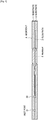
- Fig. 1 is a top schematic view illustrating a configuration of a composite structure according to the present technology.
- Fig. 2 and Fig. 3 are cross-sectional schematic views each illustrating the configuration of the composite structure according to the present technology.
- Fig. 2 corresponds to a cross section taken along a line P-P in Fig. 1
- Fig. 3 corresponds to a cross section taken along a line Q-Q in Fig. 1 .
- the composite structure denoted by a reference numeral A in the drawings is provided with substrates 11 and 12 that are bonded by thermocompression, and an embedded member 2 (hereinafter simply referred to as the "member 2") that is embedded in and bonded to the substrates 11 and 12.
- a region 3 is formed in the substrates 11 and 12 and the member 2.
- the region 3 is explained as a flow path through which liquid passes, and is referred to as the "flow path 3".
- the composite structure A is explained as a microchip that is provided for analyzing the liquid, and is referred to as the "microchip A".
- the substrates 11 and 12 are made of thermoplastic resin and bonded by thermocompression.
- the thermoplastic resin may be a known resin that is used as a microchip material.
- the thermoplastic resin include polycarbonate, polymethyl methacrylate (PMMA) resin, cyclic polyolefin, polyethylene, polystyrene, polypropylene and polydimethylsiloxane (PDMS).
- PMMA polymethyl methacrylate
- PDMS polydimethylsiloxane
- the member 2 is made of a material whose heat distortion temperature is higher than that of the thermoplastic resin that forms the substrates 11 and 12.
- the material of the member 2 include the aforementioned thermoplastic resins, metal, glass, quartz, ceramic and the like.
- the formation of the flow path 3 etc. in the member 2 can be performed by wet etching or dry etching.
- the formation of the flow path 3 etc. can be performed by machining.
- a section of the flow path 3 that is formed in the substrates 11 and 12 and a section of the flow path 3 that is formed in the member 2 are linked and connected together without displacement occurring.
- the liquid introduced into the flow path 3 can flow through the flow path 3 without any disturbance in the flow occurring at a joint between the section formed in the substrates 11 and 12 and the section formed in the member 2.
- the connecting together of the flow path 3 formed in the substrates 11 and 12 and the flow path 3 formed in the member 2 can be achieved by positioning the member 2 with respect to the substrates 11 and 12 utilizing thermal deformation of the substrates 11 and 12 that is generated during thermocompression bonding. More specifically, as shown in Fig. 3 , in the microchip A, the member 2 is fixed and held by wall surfaces 13 of the substrates 11 and 12 that have contracted due to thermal deformation, so that the substrates 11 and 12 and the member 2 are positioned. The positioning of the substrates 11 and 12 and the member 2 that is performed utilizing thermal deformation of the substrates 11 and 12 will be explained in more detail in the next section, "Manufacturing method of composite structure".
- the composite structure formed by combining the two substrates 11 and 12 and the single member 2 is exemplified as the microchip A.
- the composite structure according to the present technology may include three or more substrates and may also include two or more members. Further, here, an example is explained in which the region, such as the flow path 3 etc., is formed in each of the substrates 11 and 12. However, these regions may be all formed in one of the substrates 11 and 12.
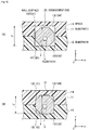
- Fig. 4 is a cross-sectional schematic view illustrating a configuration of the substrates 11 and 12.
- Fig. 4 corresponds to Fig. 2 except that the member 2 is omitted.
- Fig. 5 shows schematic views illustrating a configuration of the member 2, where (A) shows a top view, (B) shows a side view and (C) shows a front view.
- Fig. 4 is a cross-sectional schematic view illustrating a configuration of the substrates 11 and 12.
- Fig. 4 corresponds to Fig. 2 except that the member 2 is omitted.
- Fig. 5 shows schematic views illustrating a configuration
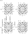
- FIG. 6 shows cross-sectional schematic views illustrating a configuration of a bonding portion between the member 2 and the substrates 11 and 12, where (A) shows the substrates 11 and 12 before thermal deformation and (B) shows the substrates 11 and 12 after thermal deformation. Note that Fig. 6 corresponds to the cross section taken along the line Q-Q in Fig. 1 .
- the substrates 11 and 12 made of thermoplastic resin and having spaces 14 are arranged.
- the spaces 14 are formed in the substrates 11 and 12 such that the member 2 can be inserted into the spaces 14 in a state in which the substrates 11 and 12 are overlapped with each other (refer to Fig. 4 ).
- each of the spaces 14 is a rectangular parallelepiped shaped space that has a surface from which the flow path 3 opens and an opposing surface that is open.
- the spaces 14 are formed using a technique, such as nanoimprinting, injection molding, machining or the like.
- Engagement ends 21 that are inserted into the spaces 14 of the substrates 11 and 12 are formed on both ends of the member 2.
- the engagement ends 21 are formed in an octagonal prism shape, and have an octagonal shape (refer to Fig. 5 (C) ) in a front view.
- the engagement ends 21 are provided on both ends of a main body of the member 2 that has a rectangular parallelepiped shape.
- the single flow path 3 is formed in the main body of the member 2 and in the two engagement ends 21.
- the member 2 formed of a material whose heat distortion temperature is higher than that of the above-described thermoplastic resin is inserted into the spaces 14.
- the engagement ends 21 are inserted into the spaces 14 formed by the overlapped substrates 11 and 12.
- Fig. 6 (A) shows a state in which the engagement ends 21 are inserted into the spaces 14.
- the insertion of the engagement ends 21 into the spaces 14 may be performed such that, after the substrate 11 and the substrate 12 are overlapped with each other, the engagement ends 21 are inserted into the spaces 14.
- the insertion can preferably be performed in the following manner. That is, first, the engagement ends 21 of the member 2 are engaged with recessed portions of the substrate 12 that form the spaces 14. Next, the substrate 11 is overlapped with the substrate 12 such that positions of recessed portions of the substrate 11 that form the spaces 14 match positions of the engagement ends 21 engaged with the substrate 12.
- an inner diameter L 1 of the spaces 14 is equal to or slightly larger than an outer diameter 1 of the engagement ends 21. Note that, even when the inner diameter L 1 of the spaces 14 is larger than the outer diameter 1 of the engagement ends 21, it is necessary for the wall surfaces 13, which form the spaces 14 and which are thermally deformed when the substrates 11 and 12 are bonded by thermocompression, to be able to come into contact with the engagement ends 21, as explained next. Note that, here, the inner diameter L 1 and the outer diameter 1 are not to be understood exclusively as those in a vertical direction (a Y-axis direction) in Fig. 6 , but are to be understood as the diameters in any direction including a horizontal direction (an X-axis direction).
- the substrates 11 and 12 are bonded by thermocompression and thus the member 2 inserted in the spaces 14 is fixed and held by the wall surfaces 13 that form each of the spaces 14 of the thermally deformed substrates 11 and 12.
- the substrates 11 and 12 are bonded by thermocompression.
- the thermocompression bonding is performed at a temperature that is higher than the heat distortion temperature of the thermoplastic resin that forms the substrates 11 and 12 and is lower than the heat distortion temperature of the material that forms the member 2.
- the substrates 11 and 12 are thermally deformed, the wall surfaces 13 that form the spaces 14 thermally contract, and the spaces 14 contract.
- the member 2 does not thermally contract as a result of the thermocompression operation.
- an inner diameter L 2 of the spaces 14 after the thermal deformation becomes smaller than the outer diameter 1 of the engagement ends 21, and each of the engagement ends 21 is fixed and held by the thermally contracted wall surfaces 13, as shown in Fig. 6 (B) .
- the substrates 11 and 12 and the member 2 are bonded together.
- the thermal contraction of the wall surfaces 13 and the contraction of the spaces 14 occur in an isotropic manner.
- four of the wall surfaces 13 that form each of the spaces 14, namely, wall surfaces 131 and 132 that face each other in the Y-axis direction and wall surfaces 133 and 134 that face each other in the X-axis direction expand uniformly to the space 14 side as a result of the thermal contraction.
- each of the engagement ends 21 is held at the center in the space 14 and is positioned by the wall surfaces 131, 132, 133 and 134 that expand by the same amount.
- the section of the flow path 3 formed in the substrates 11 and 12 and the section of the flow path 3 formed in the member 2 are linked and connected together (refer to Fig. 1 and Fig. 2 )
- the thermal contraction of the substrates 11 and 12 is utilized to hold and fix the member 2 at the center in the spaces 14.
- the sections of the flow path 3 that are respectively formed in the member 2 and in the substrates 11 and 12 can be easily and highly accurately positioned and connected together without displacement occurring.
- the inner diameter L 1 of the spaces 14 and the outer diameter 1 of the engagement ends 21 are set to appropriate diameters so that the thermally contracted wall surfaces 13 can come into close contact with each of the engagement ends 21, taking account of a thermal contraction amount of the wall surfaces 13 formed in this manner. More specifically, the inner diameter L 1 of the spaces 14 is designed in advance such that the inner diameter L 2 after the thermal deformation is smaller than the outer diameter 1 of the engagement ends 21.
- the positioning may be performed in only one direction, namely, only in the X-axis direction by the wall surfaces 131 and 132 or only in the Y-axis direction by the wall surfaces 133 and 134.
- the inner diameter L 1 of the spaces 14 in the X-axis direction may be different from that in the Y-axis direction and, in a similar manner, the outer diameter 1 of the engagement ends 21 in the X-axis direction may be different from that in the Y-axis direction.
- the positioning can be performed in a Z-axis direction (in a direction that is parallel to the flow path 3) in addition to the X-axis direction and/or the Y-axis direction.
- the shape of the spaces 14 and the shape of the engagement ends 21 such that some areas of the wall surfaces 13 do not come into contact with each of the engagement ends 21 when the wall surfaces 13 thermally contract. If whole areas of the wall surfaces 13 come into close contact with each of the engagement ends 21 when the wall surfaces 13 thermally contract, there is a risk that the member 2 is deformed and damaged by pressure of the thermoplastic resin that expands to the space 14 side.
- the spaces 14 are formed in a rectangular parallelepiped shape and the engagement ends 21 are formed in an octagonal prism shape.
- the shape of the spaces 14 and the shape of the engagement ends 21 are not limited to a combination of a rectangular parallelepiped shape and an octagonal prism shape, and may be a combination of various shapes.
- the shape of the engagement ends 21 may be a cylindrical shape.
- the spaces 14 may have an octagonal prism shape and the engagement ends 21 may have a cylindrical shape.
- a sealant may be arranged or processing using a sealant may be performed on the bonding portion between the substrates 11 and 12 and the member 2 that are bonded utilizing the thermal deformation of the substrates 11 and 12.
- Sealing can be performed by a method in which an elastic member (an O-ring etc.) made of rubber or the like is arranged on the bonding portion, a method in which an adhesive is applied to the bonding portion, or the like.
- microchip A As a specific example of an embodiment of the above-described microchip A, an example will be explained in which the microchip A is used for analyzing micro-particles. Note that the above-described Patent Literature 1 can be referred to as the microchip for analyzing micro-particles
- the member 2 made of crystal is embedded in a thermoplastic resin substrate that is formed by bonding substrates by thermocompression.
- the flow path 3 through which flows a liquid (hereinafter referred to as a "sample liquid") containing micro-particles to be analyzed, is formed in the substrate and the member 2.
- the sample liquid is introduced into the flow path 3 from a sample inlet 311.
- the micro-particles contained in the sample liquid may be biologically-relevant micro-particles, such as cells, microorganisms and liposomes, or may be synthetic particles such as latex particles, gel particles and industrial particles.
- the biologically-relevant micro-particles include chromosomes that form various types of cells, liposomes, mitochondria and organelles.
- the cells to be targeted include animal cells (hematopoietic cells etc.) and plant cells.
- the microorganisms include bacteria such as coli bacteria, viruses such as tobacco mosaic virus, fungi such as yeast, and the like.
- the biologically-relevant micro-particles can include biologically-relevant polymers, such as nucleic acid, protein and a complex of nucleic acid and protein.
- the industrial particles may be, for example, organic or inorganic polymer materials, metals, or the like.
- the organic polymer materials include polystyrene, styrene-divinylbenzene, polymethyl methacrylate, and the like.
- the inorganic polymer materials include glass, silica, magnetic materials, and the like.
- the metals include gold colloid, aluminum, and the like. Normally, the shape of these particles is a sphere. However, these particles may have a shape other than a sphere, and the size and mass of these particles are not particularly limited.
- the sample liquid is fed through the flow path 3 in a state in which the sample liquid is surrounded by a sheath liquid that is introduced from a sheath inlet 312.
- the sheath liquid introduced from the sheath inlet 312 is divided into streams in two directions and fed.
- the sheath liquid joins the sample liquid such that the streams of the sheath liquid sandwich the sample liquid from two directions.
- a three-dimensional laminar flow is formed at the confluence portion such that a sample liquid laminar flow is located in the center of a sheath liquid laminar flow.
- a reference numeral 4 denotes a suction flow path.
- the suction flow path 4 temporarily reverses the flow by applying a negative pressure to the inside of the flow path 3 in order to resolve the clogging or air bubbles.
- a suction outlet 42 is formed at one end of the suction flow path 4, to which a negative pressure source, such as a vacuum pump, is connected, while the other end of the suction flow path 4 is connected to the flow path 3 at a communication opening 41.
- the micro-particles are caused to flow through the flow path 3 such that the micro-particles are arranged in a row in the formed three-dimensional laminar flow, and are fed to a light irradiated portion that is irradiated by an optical detection device B.
- the optical detection device B includes: an irradiation system that includes a laser light source, a condenser lens that focuses/irradiates a laser beam with respect to the micro-particles, a dichroic mirror, a bandpass filter and the like; and a detection system that detects light to be measured that is emitted from the micro-particles by irradiation of the laser light.
- the detection system is formed by, for example, a photo multiplier tube (PMT), an area imaging device, such as a charge coupled device (CCD) or a complementary metal oxide semiconductor (CMOS) element, and the like.
- PMT photo multiplier tube
- CCD charge coupled device
- CMOS complementary metal oxide semiconductor
- FIG. 8 shows a case in which the irradiation system and the detection system are formed using a same optical path. However, the irradiation system and the detection system may be formed using separate optical paths.
- the light to be measured that is detected by the detection system of the optical detection device B is light emitted from the micro-particles by irradiation of measurement light.
- measurement light For example, forward scattered light, side scattered light, scattered light from Rayleigh-scattering, Mie-scattering or the like, and fluorescence can be used.
- These types of light to be measured are converted into electrical signals, and optical characteristics of the micro-particles are determined based on the electrical signals.
- the sample liquid that has passed through the light irradiated portion is discharged to a space outside the microchip A from an ejection port 321 that is provided on one end of the flow path 3.
- the sample liquid can be discharged to the space outside the microchip A as liquid droplets containing the micro-particles.
- An electric charge is applied to the discharged liquid droplets by an electrode inserted in a charging electrode inlet 5.
- a pair of electrodes are arranged to face each other such that the pair of electrodes sandwich the moving liquid droplets, along a movement direction of the discharged liquid droplets.
- the movement direction of the liquid droplets is controlled by an electric repulsive force (or a suction force) between the pair of electrodes and the liquid droplets.
- a section of the flow path 3 that forms the light irradiated portion that is irradiated by the optical detection device B is made of crystal, which is a material that has excellent optical transparency and small optical error. Therefore, irradiation efficiency of the laser beam onto the micro-particles is high and the light to be measured can be detected with a high degree of accuracy. It is therefore possible to separate and collect the micro-particles by accurately determining the optical characteristics of the micro-particles.
- the material of the member 2 is not limited to crystal as long as it is a material that has excellent optical transparency and small optical error.
- Sections of the flow path 3 that are respectively formed in the substrate and the member 2 are linked and connected together without displacement occurring, by applying the above-described manufacturing method of the composite structure according to the present technology.
- the manufacturing method of the composite structure according to the present technology if the diameter of the flow path 3 is 100 micro meter, for example, it is possible to connect the sections of the flow path 3 at a positioning accuracy of several tens of micro meter or less.
- the microchip A As a result, in the microchip A, the three-dimensional laminar flow that is formed in the flow path 3 by the sample liquid and the sheath liquid can pass through the flow path 3 without disturbance at the joint between the section of the flow path 3 formed in the substrate and the section of the flow path 3 formed in the member 2. Accordingly, in the microchip A, it is possible to accurately measure the optical characteristics of the micro-particles while precisely matching a focal position of the laser beam in the light irradiated portion with a flowing position of the micro-particles. Further, it is possible to control the movement direction of the liquid droplets and to separate and collect the liquid droplets with high precision while stabilizing the shape and size of the liquid droplets discharged from the ejection port 321 to the space outside the microchip A.
- the composite structure according to the present technology may also be configured as follows.
- the manufacturing method for a composite structure may also be configured as follows.
- the present technology is useful when obtaining a structure by combining members that are made of different materials due to constraints of manufacturing processes, such as formation ease etc., and due to functional constraints, such as optical transparency etc.
- the present technology can be used to form a high-performance structure for optical applications.
Landscapes
- Chemical & Material Sciences (AREA)
- Health & Medical Sciences (AREA)
- Analytical Chemistry (AREA)
- General Health & Medical Sciences (AREA)
- Dispersion Chemistry (AREA)
- Hematology (AREA)
- Clinical Laboratory Science (AREA)
- Chemical Kinetics & Catalysis (AREA)
- Biochemistry (AREA)
- Life Sciences & Earth Sciences (AREA)
- Physics & Mathematics (AREA)
- General Physics & Mathematics (AREA)
- Immunology (AREA)
- Pathology (AREA)
- Physical Or Chemical Processes And Apparatus (AREA)
- Micromachines (AREA)
- Lining Or Joining Of Plastics Or The Like (AREA)
- Optical Measuring Cells (AREA)
- Automatic Analysis And Handling Materials Therefor (AREA)
- Combinations Of Printed Boards (AREA)
- Laminated Bodies (AREA)
Description
- The present technology relates to a composite structure and a manufacturing method therefor. More specifically, the present technology relates to a composite structure that is formed such that a plurality of members made of materials having different heat distortion temperatures are combined utilizing thermal deformation, and to a manufacturing method therefor.
- In recent years, microchips are being developed in which ultra-precision machining technology of the semiconductor industry is applied, and a region or a flow path for chemical or biological analysis is provided on a substrate made of silicon or glass. An analysis system using this kind of microchip is referred to as a micro total analysis system (micro-TAS), a lab-on-chip system or a biochip system. The analysis system is attracting attention as a technology that can speed up the analysis, improve efficiency or promote integration, and further can reduce the size of an analyzing device.
- With micro-TAS, the analysis can be made using a small sample amount, and the microchip is disposable. For these reasons, the micro-TAS is expected to be applied, particularly, to biological analysis that uses valuable micro samples and many test substances. For example, an electrochemical detector for liquid chromatography and a small electrochemical sensor in clinical practice are known as application examples of micro-TAS.
- Further, as another application example, a micro-particle analysis technology is known that optically, electrically or magnetically analyzes characteristics of micro-particles, such as cells or micro beads, in the flow path disposed in the microchip. In the micro-particle analysis technology, a population (a group) that is determined to satisfy a predetermined condition by the analysis is separated and collected from the micro-particles.
- For example, Patent Literature 1 discloses "a microchip that includes: a flow path through which liquid containing micro-particles flows; and an orifice from which the liquid flowing through the flow path is discharged to a space outside the chip, wherein a light irradiated portion to detect optical characteristics of the micro-particles is formed at a predetermined section of the flow path". This microchip controls a movement direction of a liquid droplet containing the micro-particles discharged from the orifice. Thus, the microchip is used to separate and collect the micro-particles that are determined, at the light irradiated portion, to have a predetermined optical characteristic.
- PTL 1:
Japanese Patent Application Publication No. 2010-190680 - When the microchip is formed by combining a plurality of members, it is necessary to highly accurately position flow paths or regions that are formed in the respective members and to connect them together. As a method for positioning the flow paths etc., in related art, a very troublesome method is used in which the flow paths etc. of the respective members are connected while observing them using a microscope.
- In light of the above, it is a main object of the present technology to provide a composite structure that makes it possible to highly accurately and easily position flow paths or regions that are formed in respective members and to connect them together.
- In order to solve the above-described problems, the present technology provides a composite structure including: at least two substrates which are made of thermoplastic resin and which are bonded by thermocompression; and at least one member which is made of a material whose heat distortion temperature is higher than a heat distortion temperature of the thermoplastic resin and which is inserted into a space formed in at least one of the substrates. The member inserted in the space is fixed and held by wall surfaces which form the space of the substrates and which are thermally deformed by thermocompression.
- In the composite structure, regions that are respectively formed in at least one of the substrates and in the member are linked and connected together by determining a position of the member in the space by the thermally deformed wall surfaces.
- The composite structure may be a microchip including a flow path which is formed as the regions and through which liquid passes. The composite structure may further include a light irradiated portion where light is irradiated onto one of the liquid that flows through the flow path and a sample contained in the liquid. In this case, it is preferable that the light irradiated portion is formed by the member made of a material having optical transparency that is superior to that of the thermoplastic resin that forms the substrates.
- Further, the present technology provides a manufacturing method of a composite structure, including: arranging at least two substrates which are made of thermoplastic resin and which have a space that is formed in at least one of the substrates; inserting, into the space, at least one member that is made of a material whose heat distortion temperature is higher than a heat distortion temperature of the thermoplastic resin; and bonding the substrates by thermocompression and thereby causing wall surfaces, which form the space of the substrates and which are thermally deformed, to fix and hold the member inserted in the space.
- With the manufacturing method of the composite structure, regions that are respectively formed in at least one of the substrates and in the member can be linked and connected together by determining a position of the member in the space by the thermally deformed wall surfaces.
- In the manufacturing method of the composite structure, the thermocompression of the substrates is performed at a temperature which is higher than the heat distortion temperature of the thermoplastic resin that forms the substrates and which is lower than the heat distortion temperature of the material that forms the member.
- With the present technology, a microchip is provided that makes it possible to highly accurately and easily position flow paths or regions that are formed in respective members and to connect them together.
-
- [
fig.1]Fig. 1 is a top schematic view illustrating a configuration of a composite structure according to the present technology. - [
fig.2]Fig. 2 is a cross-sectional schematic view (a cross section taken along a line P-P inFig. 1 ) illustrating the configuration of the composite structure according to the present technology. - [
fig.3]Fig. 3 is a cross-sectional schematic view (a cross section taken along a line Q-Q inFig. 1 ) illustrating the configuration of the composite structure according to the present technology. - [
fig.4]Fig. 4 is a cross-sectional schematic view illustrating a configuration ofsubstrates - [
fig.5]Fig. 5 shows schematic views illustrating a configuration of amember 2, where (A) shows a top view, (B) shows a side view and (C) shows a front view. - [
fig.6]Fig. 6 shows cross-sectional schematic views illustrating a configuration of a bonding portion between themember 2 and thesubstrates substrates substrates - [
fig.7]Fig. 7 shows cross-sectional schematic views illustrating a configuration of a modified example of the bonding portion between themember 2 and thesubstrates substrates substrates - [
fig.8]Fig. 8 is a schematic view illustrating a specific example of an embodiment of the composite structure according to the present technology. - Hereinafter, preferred embodiments of the present disclosure will be described in detail with reference to the appended drawings. Note that, in this specification and the appended drawings, structural elements that have substantially the same function and structure are denoted with the same reference numerals, and repeated explanation of these structural elements is omitted. The explanation will be made in the following order.
- 1. Composite structure
- 2. Manufacturing method of composite structure
- 3. Microchip for analyzing micro-particles
-
Fig. 1 is a top schematic view illustrating a configuration of a composite structure according to the present technology.Fig. 2 andFig. 3 are cross-sectional schematic views each illustrating the configuration of the composite structure according to the present technology.Fig. 2 corresponds to a cross section taken along a line P-P inFig. 1 , andFig. 3 corresponds to a cross section taken along a line Q-Q inFig. 1 . - The composite structure denoted by a reference numeral A in the drawings is provided with
substrates member 2") that is embedded in and bonded to thesubstrates region 3 is formed in thesubstrates member 2. Hereinafter, theregion 3 is explained as a flow path through which liquid passes, and is referred to as the "flow path 3". Further, the composite structure A is explained as a microchip that is provided for analyzing the liquid, and is referred to as the "microchip A". - The
substrates flow path 3,inlet ports 31, which introduce liquid to be analyzed or liquid containing an analysis target object into theflow path 3 from the outside, and adischarge port 32, which discharges the liquid from the inside of theflow path 3 to the outside, are formed in thesubstrates - The thermoplastic resin may be a known resin that is used as a microchip material. Examples of the thermoplastic resin include polycarbonate, polymethyl methacrylate (PMMA) resin, cyclic polyolefin, polyethylene, polystyrene, polypropylene and polydimethylsiloxane (PDMS). The formation of the
flow path 3 etc. in thesubstrates 11 I and 12 can be performed using a known technique, such as nanoimprinting, injection molding, machining or the like. - The
member 2 is made of a material whose heat distortion temperature is higher than that of the thermoplastic resin that forms thesubstrates member 2 include the aforementioned thermoplastic resins, metal, glass, quartz, ceramic and the like. For example, when themember 2 is made of glass, the formation of theflow path 3 etc. in themember 2 can be performed by wet etching or dry etching. Further, for example, when themember 2 is made of metal, the formation of theflow path 3 etc. can be performed by machining. - As shown in
Fig. 1 andFig. 2 , a section of theflow path 3 that is formed in thesubstrates flow path 3 that is formed in themember 2 are linked and connected together without displacement occurring. Thus, the liquid introduced into theflow path 3 can flow through theflow path 3 without any disturbance in the flow occurring at a joint between the section formed in thesubstrates member 2. - The connecting together of the
flow path 3 formed in thesubstrates flow path 3 formed in themember 2 can be achieved by positioning themember 2 with respect to thesubstrates substrates Fig. 3 , in the microchip A, themember 2 is fixed and held bywall surfaces 13 of thesubstrates substrates member 2 are positioned. The positioning of thesubstrates member 2 that is performed utilizing thermal deformation of thesubstrates - Here, the composite structure formed by combining the two
substrates single member 2 is exemplified as the microchip A. However, the composite structure according to the present technology may include three or more substrates and may also include two or more members. Further, here, an example is explained in which the region, such as theflow path 3 etc., is formed in each of thesubstrates substrates - Next, a manufacturing method of the composite structure according to the present technology will be explained with reference to
Fig. 4 to Fig. 6 , taking the above-described microchip A as an example.Fig. 4 is a cross-sectional schematic view illustrating a configuration of thesubstrates Fig. 4 corresponds toFig. 2 except that themember 2 is omitted.Fig. 5 shows schematic views illustrating a configuration of themember 2, where (A) shows a top view, (B) shows a side view and (C) shows a front view.Fig. 6 shows cross-sectional schematic views illustrating a configuration of a bonding portion between themember 2 and thesubstrates substrates substrates Fig. 6 corresponds to the cross section taken along the line Q-Q inFig. 1 . - Firstly, a first process will be explained. In the first process, the
substrates spaces 14 are arranged. In the first process, thespaces 14 are formed in thesubstrates member 2 can be inserted into thespaces 14 in a state in which thesubstrates Fig. 4 ). When thesubstrates spaces 14 is a rectangular parallelepiped shaped space that has a surface from which theflow path 3 opens and an opposing surface that is open. In a similar manner to theflow path 3, thespaces 14 are formed using a technique, such as nanoimprinting, injection molding, machining or the like. - Engagement ends 21 that are inserted into the
spaces 14 of thesubstrates member 2. The engagement ends 21 are formed in an octagonal prism shape, and have an octagonal shape (refer toFig. 5 (C) ) in a front view. The engagement ends 21 are provided on both ends of a main body of themember 2 that has a rectangular parallelepiped shape. Thesingle flow path 3 is formed in the main body of themember 2 and in the two engagement ends 21. - Next, a second process will be explained. In the second process, the
member 2 formed of a material whose heat distortion temperature is higher than that of the above-described thermoplastic resin is inserted into thespaces 14. In the second process, the engagement ends 21 are inserted into thespaces 14 formed by the overlappedsubstrates Fig. 6 (A) shows a state in which the engagement ends 21 are inserted into thespaces 14. The insertion of the engagement ends 21 into thespaces 14 may be performed such that, after thesubstrate 11 and thesubstrate 12 are overlapped with each other, the engagement ends 21 are inserted into thespaces 14. However, the insertion can preferably be performed in the following manner. That is, first, the engagement ends 21 of themember 2 are engaged with recessed portions of thesubstrate 12 that form thespaces 14. Next, thesubstrate 11 is overlapped with thesubstrate 12 such that positions of recessed portions of thesubstrate 11 that form thespaces 14 match positions of the engagement ends 21 engaged with thesubstrate 12. - In order to easily insert the engagement ends 21 into the
spaces 14, it is preferable that an inner diameter L1 of thespaces 14 is equal to or slightly larger than an outer diameter 1 of the engagement ends 21. Note that, even when the inner diameter L1 of thespaces 14 is larger than the outer diameter 1 of the engagement ends 21, it is necessary for the wall surfaces 13, which form thespaces 14 and which are thermally deformed when thesubstrates Fig. 6 , but are to be understood as the diameters in any direction including a horizontal direction (an X-axis direction). - Next, a third process will be explained. In the third process, the
substrates member 2 inserted in thespaces 14 is fixed and held by the wall surfaces 13 that form each of thespaces 14 of the thermallydeformed substrates spaces 14, thesubstrates substrates member 2. As a result of this thermocompression operation, thesubstrates spaces 14 thermally contract, and thespaces 14 contract. On the other hand, themember 2 does not thermally contract as a result of the thermocompression operation. Thus, an inner diameter L2 of thespaces 14 after the thermal deformation becomes smaller than the outer diameter 1 of the engagement ends 21, and each of the engagement ends 21 is fixed and held by the thermally contracted wall surfaces 13, as shown inFig. 6 (B) . Thus, thesubstrates member 2 are bonded together. - When the thermocompression operation is performed, the thermal contraction of the wall surfaces 13 and the contraction of the
spaces 14 occur in an isotropic manner. Specifically, four of the wall surfaces 13 that form each of thespaces 14, namely, wall surfaces 131 and 132 that face each other in the Y-axis direction and wall surfaces 133 and 134 that face each other in the X-axis direction, expand uniformly to thespace 14 side as a result of the thermal contraction. Thus, each of the engagement ends 21 is held at the center in thespace 14 and is positioned by the wall surfaces 131, 132, 133 and 134 that expand by the same amount. Then, the section of theflow path 3 formed in thesubstrates flow path 3 formed in themember 2 are linked and connected together (refer toFig. 1 andFig. 2 ) - In this manner, the thermal contraction of the
substrates member 2 at the center in thespaces 14. Thus, the sections of theflow path 3 that are respectively formed in themember 2 and in thesubstrates - The inner diameter L1 of the
spaces 14 and the outer diameter 1 of the engagement ends 21 are set to appropriate diameters so that the thermally contracted wall surfaces 13 can come into close contact with each of the engagement ends 21, taking account of a thermal contraction amount of the wall surfaces 13 formed in this manner. More specifically, the inner diameter L1 of thespaces 14 is designed in advance such that the inner diameter L2 after the thermal deformation is smaller than the outer diameter 1 of the engagement ends 21. - Here, a case is explained in which positioning of each of the engagement ends 21 is performed inside the
space 14 in both the X-axis direction and the Y-axis direction. However, the positioning may be performed in only one direction, namely, only in the X-axis direction by the wall surfaces 131 and 132 or only in the Y-axis direction by the wall surfaces 133 and 134. When the positioning is performed in only one direction, the inner diameter L1 of thespaces 14 in the X-axis direction may be different from that in the Y-axis direction and, in a similar manner, the outer diameter 1 of the engagement ends 21 in the X-axis direction may be different from that in the Y-axis direction. Further, the positioning can be performed in a Z-axis direction (in a direction that is parallel to the flow path 3) in addition to the X-axis direction and/or the Y-axis direction. - Further, it is preferable to design the shape of the
spaces 14 and the shape of the engagement ends 21 such that some areas of the wall surfaces 13 do not come into contact with each of the engagement ends 21 when the wall surfaces 13 thermally contract. If whole areas of the wall surfaces 13 come into close contact with each of the engagement ends 21 when the wall surfaces 13 thermally contract, there is a risk that themember 2 is deformed and damaged by pressure of the thermoplastic resin that expands to thespace 14 side. In order to avoid this, here, thespaces 14 are formed in a rectangular parallelepiped shape and the engagement ends 21 are formed in an octagonal prism shape. Thus, when thespaces 14 thermally contract, four of the eight surfaces of each of the engagement ends 21 do not come into contact with the wall surfaces 13 and gaps are formed between the wall surfaces 13 and the four surfaces. As a result, these gaps serve as escapes for the expanded thermoplastic resin and inhibit an excessive pressure from being applied to themember 2. - The shape of the
spaces 14 and the shape of the engagement ends 21 are not limited to a combination of a rectangular parallelepiped shape and an octagonal prism shape, and may be a combination of various shapes. For example, as shown inFig. 7 (A) and Fig. 7 (B) , the shape of the engagement ends 21 may be a cylindrical shape. Further, for example, as shown inFig. 7 (C) and Fig. 7 (D) , thespaces 14 may have an octagonal prism shape and the engagement ends 21 may have a cylindrical shape. In either case, when the wall surfaces 13 thermally contract, some areas of the wall surfaces 13 come into close contact with each of the engagement ends 21 and function to position each of the engagement ends 21 in thespaces 14, while the other areas of the wall surfaces 13 form gaps with each of the engagement ends 21 and function to inhibit an excessive pressure being applying to themember 2. - In order to improve liquid tightness, a sealant may be arranged or processing using a sealant may be performed on the bonding portion between the
substrates member 2 that are bonded utilizing the thermal deformation of thesubstrates - As a specific example of an embodiment of the above-described microchip A, an example will be explained in which the microchip A is used for analyzing micro-particles. Note that the above-described Patent Literature 1 can be referred to as the microchip for analyzing micro-particles
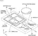
- In the microchip A shown in
FIG. 8 , themember 2 made of crystal is embedded in a thermoplastic resin substrate that is formed by bonding substrates by thermocompression. Theflow path 3, through which flows a liquid (hereinafter referred to as a "sample liquid") containing micro-particles to be analyzed, is formed in the substrate and themember 2. - The sample liquid is introduced into the
flow path 3 from asample inlet 311. The micro-particles contained in the sample liquid may be biologically-relevant micro-particles, such as cells, microorganisms and liposomes, or may be synthetic particles such as latex particles, gel particles and industrial particles. The biologically-relevant micro-particles include chromosomes that form various types of cells, liposomes, mitochondria and organelles. The cells to be targeted include animal cells (hematopoietic cells etc.) and plant cells. The microorganisms include bacteria such as coli bacteria, viruses such as tobacco mosaic virus, fungi such as yeast, and the like. Further, it is assumed that the biologically-relevant micro-particles can include biologically-relevant polymers, such as nucleic acid, protein and a complex of nucleic acid and protein. Further, the industrial particles may be, for example, organic or inorganic polymer materials, metals, or the like. The organic polymer materials include polystyrene, styrene-divinylbenzene, polymethyl methacrylate, and the like. The inorganic polymer materials include glass, silica, magnetic materials, and the like. The metals include gold colloid, aluminum, and the like. Normally, the shape of these particles is a sphere. However, these particles may have a shape other than a sphere, and the size and mass of these particles are not particularly limited. - The sample liquid is fed through the
flow path 3 in a state in which the sample liquid is surrounded by a sheath liquid that is introduced from asheath inlet 312. The sheath liquid introduced from thesheath inlet 312 is divided into streams in two directions and fed. After that, at a confluence portion with the sample liquid introduced from thesample inlet 311, the sheath liquid joins the sample liquid such that the streams of the sheath liquid sandwich the sample liquid from two directions. Thus, a three-dimensional laminar flow is formed at the confluence portion such that a sample liquid laminar flow is located in the center of a sheath liquid laminar flow. - A
reference numeral 4 denotes a suction flow path. When clogging or air bubbles occur in theflow path 3, thesuction flow path 4 temporarily reverses the flow by applying a negative pressure to the inside of theflow path 3 in order to resolve the clogging or air bubbles. Asuction outlet 42 is formed at one end of thesuction flow path 4, to which a negative pressure source, such as a vacuum pump, is connected, while the other end of thesuction flow path 4 is connected to theflow path 3 at acommunication opening 41. - The micro-particles are caused to flow through the
flow path 3 such that the micro-particles are arranged in a row in the formed three-dimensional laminar flow, and are fed to a light irradiated portion that is irradiated by an optical detection device B. The optical detection device B includes: an irradiation system that includes a laser light source, a condenser lens that focuses/irradiates a laser beam with respect to the micro-particles, a dichroic mirror, a bandpass filter and the like; and a detection system that detects light to be measured that is emitted from the micro-particles by irradiation of the laser light. The detection system is formed by, for example, a photo multiplier tube (PMT), an area imaging device, such as a charge coupled device (CCD) or a complementary metal oxide semiconductor (CMOS) element, and the like. Note that, inFIG. 8 , only the condenser lens is shown as the optical detection device B. Further,FIG. 8 shows a case in which the irradiation system and the detection system are formed using a same optical path. However, the irradiation system and the detection system may be formed using separate optical paths. - The light to be measured that is detected by the detection system of the optical detection device B is light emitted from the micro-particles by irradiation of measurement light. For example, forward scattered light, side scattered light, scattered light from Rayleigh-scattering, Mie-scattering or the like, and fluorescence can be used. These types of light to be measured are converted into electrical signals, and optical characteristics of the micro-particles are determined based on the electrical signals.
- The sample liquid that has passed through the light irradiated portion is discharged to a space outside the microchip A from an
ejection port 321 that is provided on one end of theflow path 3. At this time, if the microchip A is vibrated by a vibrating element, the sample liquid can be discharged to the space outside the microchip A as liquid droplets containing the micro-particles. An electric charge is applied to the discharged liquid droplets by an electrode inserted in a chargingelectrode inlet 5. - In the space outside the microchip A, a pair of electrodes are arranged to face each other such that the pair of electrodes sandwich the moving liquid droplets, along a movement direction of the discharged liquid droplets. The movement direction of the liquid droplets is controlled by an electric repulsive force (or a suction force) between the pair of electrodes and the liquid droplets. Thus, the micro-particles contained in the liquid droplets are separated and collected in accordance with the optical characteristics of the micro-particles.
- In the microchip A, a section of the
flow path 3 that forms the light irradiated portion that is irradiated by the optical detection device B is made of crystal, which is a material that has excellent optical transparency and small optical error. Therefore, irradiation efficiency of the laser beam onto the micro-particles is high and the light to be measured can be detected with a high degree of accuracy. It is therefore possible to separate and collect the micro-particles by accurately determining the optical characteristics of the micro-particles. - Further, only the light irradiated portion of the microchip A is made of crystal, which is expensive, and the other portions are made of thermoplastic resin, which is cheap and easily formed. Thus, it is also possible to reduce the cost of the entire microchip A. Note that the material of the
member 2 is not limited to crystal as long as it is a material that has excellent optical transparency and small optical error. - Sections of the
flow path 3 that are respectively formed in the substrate and themember 2 are linked and connected together without displacement occurring, by applying the above-described manufacturing method of the composite structure according to the present technology. With the manufacturing method of the composite structure according to the present technology, if the diameter of theflow path 3 is 100 micro meter, for example, it is possible to connect the sections of theflow path 3 at a positioning accuracy of several tens of micro meter or less. - As a result, in the microchip A, the three-dimensional laminar flow that is formed in the
flow path 3 by the sample liquid and the sheath liquid can pass through theflow path 3 without disturbance at the joint between the section of theflow path 3 formed in the substrate and the section of theflow path 3 formed in themember 2. Accordingly, in the microchip A, it is possible to accurately measure the optical characteristics of the micro-particles while precisely matching a focal position of the laser beam in the light irradiated portion with a flowing position of the micro-particles. Further, it is possible to control the movement direction of the liquid droplets and to separate and collect the liquid droplets with high precision while stabilizing the shape and size of the liquid droplets discharged from theejection port 321 to the space outside the microchip A. - It should be understood by those skilled in the art that various modifications, combinations, sub-combinations and alterations may occur depending on design requirements and other factors insofar as they are within the scope of the appended claims or the equivalents thereof.
- The composite structure according to the present technology may also be configured as follows.
- (1) A composite structure comprising:
- at least two substrates which are made of thermoplastic resin and which are bonded by thermocompression; and
- at least one member which is made of a material whose heat distortion temperature is higher than a heat distortion temperature of the thermoplastic resin and which is inserted into a space formed in at least one of the substrates,
- wherein the member inserted in the space is fixed and held by wall surfaces which form the space of the substrates and which are thermally deformed by thermocompression.
- (2) The composite structure according to (1), wherein
a position of the member in the space is determined by the wall surfaces. - (3) The composite structure according to (1) or (2), wherein
the member is positioned in the space such that regions that are respectively formed in at least one of the substrates and in the member are linked. - (4) The composite structure according to (3), wherein
the composite structure is a microchip including a flow path which is formed as the regions and through which liquid passes. - (5) The composite structure according to (4), further comprising:
- a light irradiated portion where light is irradiated onto one of the liquid that flows through the flow path and a sample contained in the liquid,
- wherein the light irradiated portion is formed by the member made of a material having optical transparency that is superior to that of the thermoplastic resin that forms the substrates.
- In addition, the manufacturing method for a composite structure may also be configured as follows.
- (1) A manufacturing method for a composite structure, comprising:
- arranging at least two substrates which are made of thermoplastic resin and which have a space that is formed in at least one of the substrates;
- inserting, into the space, at least one member that is made of a material whose heat distortion temperature is higher than a heat distortion temperature of the thermoplastic resin; and
- bonding the substrates by thermocompression and thereby causing wall surfaces, which form the space of the substrates and which are thermally deformed, to fix and hold the member inserted in the space.
- (2) The manufacturing method according to (1), wherein
in the step of causing the wall surfaces to fix and hold the member, a position of the member in the space is determined by the wall surfaces. - (3) The manufacturing method according to (1) or (2), wherein
in the step of causing the wall surfaces to fix and hold the member, the member is positioned in the space such that regions that are respectively formed in at least one of the substrates and in the member are linked. - (4) The manufacturing method according to any one of (1) to (3), wherein
in the step of causing the wall surfaces to fix and hold the member, the thermocompression of the substrates is performed at a temperature which is higher than the heat distortion temperature of the thermoplastic resin that forms the substrates and which is lower than the heat distortion temperature of the material that forms the member. - With the composite structure and the manufacturing method therefor according to the present technology, a plurality of members made of different materials can be easily and highly accurately positioned and combined, and an allowance for a tolerance of the members can be increased by combining the members utilizing thermal contraction of the members. Therefore, the present technology is useful when obtaining a structure by combining members that are made of different materials due to constraints of manufacturing processes, such as formation ease etc., and due to functional constraints, such as optical transparency etc. For example, the present technology can be used to form a high-performance structure for optical applications.
-
- A
- Microchip
- B
- Optical detection device
- 11, 12
- Substrate
- 13, 131, 132, 133, 134
- Wall surface
- 14
- Space
- 2
- Embedded member
- 21
- Engagement end
- 3
- Flow path
- 31
- Inlet port
- 311
- Sample inlet
- 312
- Sheath inlet
- 32
- Discharge port
- 321
- Ejection port
- 4
- Suction flow path
- 41
- Communication opening
- 42
- Suction outlet
- 5
- Charging electrode inlet
Claims (9)
- A composite structure comprising:at least two substrates (11, 12) which are made of thermoplastic resin and which are bonded by thermocompression; andat least one member (2) which is made of a material whose heat distortion temperature is higher than a heat distortion temperature of the thermoplastic resin and which is inserted into a space (14) formed in at least one of the substrates (11, 12),wherein the member (2) inserted in the space (14) is fixed and held by wall surfaces (13) which form the space (14) of the substrates (11, 12) and which are thermally deformed by thermocompression.
- The composite structure according to claim 1, wherein
a position of the member (2) in the space (14) is determined by the wall surfaces (13). - The composite structure according to claim 2, wherein
the member (2) is positioned in the space (14) such that regions that are respectively formed in at least one of the substrates (11, 12) and in the member (2) are linked. - The composite structure according to claim 3, wherein
the composite structure is a microchip including a flow path (3) which is formed as the regions and through which liquid passes. - The composite structure according to claim 4, further comprising:a light irradiated portion where light is irradiated onto one of the liquid that flows through the flow path and a sample contained in the liquid,wherein the light irradiated portion is formed by the member (2) made of a material having optical transparency that is superior to that of the thermoplastic resin that forms the substrates (11, 12).
- A manufacturing method for a composite structure, comprising:arranging at least two substrates (11, 12) which are made of thermoplastic resin and which have a space (14) that is formed in at least one of the substrates (11, 12);inserting, into the space (14), at least one member (2) that is made of a material whose heat distortion temperature is higher than a heat distortion temperature of the thermoplastic resin; andbonding the substrates (11, 12) by thermocompression and thereby causing wall surfaces (13), which form the space (14) of the substrates (11, 12) and which are thermally deformed, to fix and hold the member (2) inserted in the space (14).
- The manufacturing method according to claim 6, wherein
in the step of causing the wall surfaces (13) to fix and hold the member (2), a position of the member (2) in the space (14) is determined by the wall surfaces (13). - The manufacturing method according to claim 7, wherein
in the step of causing the wall surfaces (13) to fix and hold the member (2), the member (2) is positioned in the space (14) such that regions that are respectively formed in at least one of the substrates (11, 12) and in the member (2) are linked. - The manufacturing method according to claim 8, wherein
in the step of causing the wall surfaces (13) to fix and hold the member (2), the thermocompression of the substrates (11, 12) is performed at a temperature which is higher than the heat distortion temperature of the thermoplastic resin that forms the substrates (11, 12) and which is lower than the heat distortion temperature of the material that forms the member (2).
Applications Claiming Priority (2)
| Application Number | Priority Date | Filing Date | Title |
|---|---|---|---|
| JP2011158723A JP5974429B2 (en) | 2011-07-20 | 2011-07-20 | Composite material structure and manufacturing method thereof |
| PCT/JP2012/003939 WO2013011629A1 (en) | 2011-07-20 | 2012-06-15 | Composite structure and manufacturing method therefor |
Publications (2)
| Publication Number | Publication Date |
|---|---|
| EP2734361A1 EP2734361A1 (en) | 2014-05-28 |
| EP2734361B1 true EP2734361B1 (en) | 2017-08-09 |
Family
ID=46420487
Family Applications (1)
| Application Number | Title | Priority Date | Filing Date |
|---|---|---|---|
| EP12731185.0A Not-in-force EP2734361B1 (en) | 2011-07-20 | 2012-06-15 | Composite structure and manufacturing method therefor |
Country Status (6)
| Country | Link |
|---|---|
| US (2) | US9610750B2 (en) |
| EP (1) | EP2734361B1 (en) |
| JP (1) | JP5974429B2 (en) |
| CN (2) | CN103702826B (en) |
| IN (1) | IN2014DN00261A (en) |
| WO (1) | WO2013011629A1 (en) |
Families Citing this family (2)
| Publication number | Priority date | Publication date | Assignee | Title |
|---|---|---|---|---|
| CN108393103A (en) * | 2018-03-03 | 2018-08-14 | 北京工业大学 | A kind of achievable drop size does not depend on the micro-fluidic chip of flow |
| US11665929B2 (en) * | 2019-06-13 | 2023-05-30 | Intel Corporation | Micro light-emitting diode displays with improved power efficiency |
Family Cites Families (22)
| Publication number | Priority date | Publication date | Assignee | Title |
|---|---|---|---|---|
| JPH0524516Y2 (en) * | 1987-04-21 | 1993-06-22 | ||
| JPH03156888A (en) * | 1989-08-28 | 1991-07-04 | Toshiba Corp | Dispersion type el panel and manufacture thereof |
| GB8926294D0 (en) * | 1989-11-21 | 1990-01-10 | British Gas Plc | Method of jointing hollow members by fusion |
| US5427663A (en) * | 1993-06-08 | 1995-06-27 | British Technology Group Usa Inc. | Microlithographic array for macromolecule and cell fractionation |
| GB9418981D0 (en) | 1994-09-21 | 1994-11-09 | Univ Glasgow | Apparatus and method for carrying out analysis of samples |
| JP3388392B2 (en) * | 1999-06-02 | 2003-03-17 | 日精樹脂工業株式会社 | IC card manufacturing equipment |
| EP1324828A1 (en) * | 2000-10-06 | 2003-07-09 | Protasis Corporation | Fluid separation conduit cartridge with encryption capability |
| US6564475B2 (en) * | 2000-12-22 | 2003-05-20 | K-Swiss Inc. | Footwear with enhanced temperature control |
| DE60321376D1 (en) | 2002-12-04 | 2008-07-10 | Spinx Inc | DEVICES AND METHOD FOR PROGRAMMABLE MICRO-HANDLING OF FLUIDS |
| JP4074921B2 (en) * | 2003-03-14 | 2008-04-16 | 日本電気株式会社 | Mass spectrometry system and analysis method |
| JP4695851B2 (en) | 2003-07-10 | 2011-06-08 | シチズンホールディングス株式会社 | Micro chemical chip temperature controller |
| JP4304120B2 (en) * | 2004-04-30 | 2009-07-29 | ベイバイオサイエンス株式会社 | Apparatus and method for sorting biological particles |
| CN1687766A (en) | 2005-04-21 | 2005-10-26 | 复旦大学 | Fibrous electrophoresis chip and preparation method |
| CN101175572A (en) * | 2005-05-19 | 2008-05-07 | 皇家飞利浦电子股份有限公司 | Functional assembly and method of obtaining it |
| JP4695977B2 (en) * | 2005-12-21 | 2011-06-08 | 東ソー・クォーツ株式会社 | Microchip and manufacturing method thereof |
| JP2007263706A (en) * | 2006-03-28 | 2007-10-11 | Aisin Seiki Co Ltd | Microchip for bioassay |
| US8312646B2 (en) * | 2006-05-25 | 2012-11-20 | Nike, Inc. | Article of footwear incorporating a tensile element |
| EP1972909A1 (en) | 2007-03-23 | 2008-09-24 | Koninklijke Philips Electronics N.V. | Luminescence sensor |
| US7880108B2 (en) * | 2007-10-26 | 2011-02-01 | Becton, Dickinson And Company | Deflection plate |
| JP2009243965A (en) * | 2008-03-28 | 2009-10-22 | Sumitomo Bakelite Co Ltd | Flow path device, flow path device with exterior case, method for using flow path device |
| JP4572973B2 (en) * | 2008-06-16 | 2010-11-04 | ソニー株式会社 | Microchip and flow-feeding method in microchip |
| JP5487638B2 (en) | 2009-02-17 | 2014-05-07 | ソニー株式会社 | Apparatus for microparticle sorting and microchip |
-
2011
- 2011-07-20 JP JP2011158723A patent/JP5974429B2/en active Active
-
2012
- 2012-06-15 US US14/131,730 patent/US9610750B2/en active Active
- 2012-06-15 IN IN261DEN2014 patent/IN2014DN00261A/en unknown
- 2012-06-15 CN CN201280034743.XA patent/CN103702826B/en active Active
- 2012-06-15 WO PCT/JP2012/003939 patent/WO2013011629A1/en active Application Filing
- 2012-06-15 EP EP12731185.0A patent/EP2734361B1/en not_active Not-in-force
- 2012-06-15 CN CN201510420058.6A patent/CN105126940B/en active Active
-
2017
- 2017-02-28 US US15/444,906 patent/US10414118B2/en active Active
Also Published As
| Publication number | Publication date |
|---|---|
| JP5974429B2 (en) | 2016-08-23 |
| US10414118B2 (en) | 2019-09-17 |
| WO2013011629A1 (en) | 2013-01-24 |
| US20170203296A1 (en) | 2017-07-20 |
| IN2014DN00261A (en) | 2015-06-05 |
| CN103702826A (en) | 2014-04-02 |
| JP2013022804A (en) | 2013-02-04 |
| US9610750B2 (en) | 2017-04-04 |
| US20140154475A1 (en) | 2014-06-05 |
| EP2734361A1 (en) | 2014-05-28 |
| CN103702826B (en) | 2015-08-19 |
| CN105126940A (en) | 2015-12-09 |
| CN105126940B (en) | 2018-05-18 |
Similar Documents
| Publication | Publication Date | Title |
|---|---|---|
| US10315194B2 (en) | Chip device and a particle analyzing apparatus | |
| US9861984B2 (en) | Microchip and channel structure for the same | |
| JP4572973B2 (en) | Microchip and flow-feeding method in microchip | |
| US20080311005A1 (en) | Apparatus for focusing and detecting particles in sample and method of manufacturing the same | |
| CN112261996B (en) | Microfluidic device, method for the production thereof and use thereof | |
| KR20110123210A (en) | Microparticle sorting apparatus, microchip and microchip module | |
| CN110382117A (en) | Microchip and microparticle measuring device | |
| US10414118B2 (en) | Microchip manufactured with thermocompression | |
| US10919035B2 (en) | Microchip, analysis apparatus, and analysis method | |
| JP5316530B2 (en) | Microchip and its channel structure | |
| JP2009276119A (en) | Flow channel structure and microchip |
Legal Events
| Date | Code | Title | Description |
|---|---|---|---|
| PUAI | Public reference made under article 153(3) epc to a published international application that has entered the european phase |
Free format text: ORIGINAL CODE: 0009012 |
|
| 17P | Request for examination filed |
Effective date: 20131015 |
|
| AK | Designated contracting states |
Kind code of ref document: A1 Designated state(s): AL AT BE BG CH CY CZ DE DK EE ES FI FR GB GR HR HU IE IS IT LI LT LU LV MC MK MT NL NO PL PT RO RS SE SI SK SM TR |
|
| DAX | Request for extension of the european patent (deleted) | ||
| GRAP | Despatch of communication of intention to grant a patent |
Free format text: ORIGINAL CODE: EPIDOSNIGR1 |
|
| STAA | Information on the status of an ep patent application or granted ep patent |
Free format text: STATUS: GRANT OF PATENT IS INTENDED |
|
| INTG | Intention to grant announced |
Effective date: 20170119 |
|
| GRAS | Grant fee paid |
Free format text: ORIGINAL CODE: EPIDOSNIGR3 |
|
| GRAA | (expected) grant |
Free format text: ORIGINAL CODE: 0009210 |
|
| STAA | Information on the status of an ep patent application or granted ep patent |
Free format text: STATUS: THE PATENT HAS BEEN GRANTED |
|
| AK | Designated contracting states |
Kind code of ref document: B1 Designated state(s): AL AT BE BG CH CY CZ DE DK EE ES FI FR GB GR HR HU IE IS IT LI LT LU LV MC MK MT NL NO PL PT RO RS SE SI SK SM TR |
|
| REG | Reference to a national code |
Ref country code: GB Ref legal event code: FG4D |
|
| REG | Reference to a national code |
Ref country code: CH Ref legal event code: EP Ref country code: AT Ref legal event code: REF Ref document number: 916359 Country of ref document: AT Kind code of ref document: T Effective date: 20170815 |
|
| REG | Reference to a national code |
Ref country code: IE Ref legal event code: FG4D |
|
| REG | Reference to a national code |
Ref country code: DE Ref legal event code: R096 Ref document number: 602012035637 Country of ref document: DE |
|
| REG | Reference to a national code |
Ref country code: NL Ref legal event code: MP Effective date: 20170809 |
|
| REG | Reference to a national code |
Ref country code: LT Ref legal event code: MG4D |
|
| REG | Reference to a national code |
Ref country code: AT Ref legal event code: MK05 Ref document number: 916359 Country of ref document: AT Kind code of ref document: T Effective date: 20170809 |
|
| PG25 | Lapsed in a contracting state [announced via postgrant information from national office to epo] |
Ref country code: SE Free format text: LAPSE BECAUSE OF FAILURE TO SUBMIT A TRANSLATION OF THE DESCRIPTION OR TO PAY THE FEE WITHIN THE PRESCRIBED TIME-LIMIT Effective date: 20170809 Ref country code: AT Free format text: LAPSE BECAUSE OF FAILURE TO SUBMIT A TRANSLATION OF THE DESCRIPTION OR TO PAY THE FEE WITHIN THE PRESCRIBED TIME-LIMIT Effective date: 20170809 Ref country code: FI Free format text: LAPSE BECAUSE OF FAILURE TO SUBMIT A TRANSLATION OF THE DESCRIPTION OR TO PAY THE FEE WITHIN THE PRESCRIBED TIME-LIMIT Effective date: 20170809 Ref country code: HR Free format text: LAPSE BECAUSE OF FAILURE TO SUBMIT A TRANSLATION OF THE DESCRIPTION OR TO PAY THE FEE WITHIN THE PRESCRIBED TIME-LIMIT Effective date: 20170809 Ref country code: LT Free format text: LAPSE BECAUSE OF FAILURE TO SUBMIT A TRANSLATION OF THE DESCRIPTION OR TO PAY THE FEE WITHIN THE PRESCRIBED TIME-LIMIT Effective date: 20170809 Ref country code: NL Free format text: LAPSE BECAUSE OF FAILURE TO SUBMIT A TRANSLATION OF THE DESCRIPTION OR TO PAY THE FEE WITHIN THE PRESCRIBED TIME-LIMIT Effective date: 20170809 Ref country code: NO Free format text: LAPSE BECAUSE OF FAILURE TO SUBMIT A TRANSLATION OF THE DESCRIPTION OR TO PAY THE FEE WITHIN THE PRESCRIBED TIME-LIMIT Effective date: 20171109 |
|
| PG25 | Lapsed in a contracting state [announced via postgrant information from national office to epo] |
Ref country code: IS Free format text: LAPSE BECAUSE OF FAILURE TO SUBMIT A TRANSLATION OF THE DESCRIPTION OR TO PAY THE FEE WITHIN THE PRESCRIBED TIME-LIMIT Effective date: 20171209 Ref country code: ES Free format text: LAPSE BECAUSE OF FAILURE TO SUBMIT A TRANSLATION OF THE DESCRIPTION OR TO PAY THE FEE WITHIN THE PRESCRIBED TIME-LIMIT Effective date: 20170809 Ref country code: GR Free format text: LAPSE BECAUSE OF FAILURE TO SUBMIT A TRANSLATION OF THE DESCRIPTION OR TO PAY THE FEE WITHIN THE PRESCRIBED TIME-LIMIT Effective date: 20171110 Ref country code: LV Free format text: LAPSE BECAUSE OF FAILURE TO SUBMIT A TRANSLATION OF THE DESCRIPTION OR TO PAY THE FEE WITHIN THE PRESCRIBED TIME-LIMIT Effective date: 20170809 Ref country code: PL Free format text: LAPSE BECAUSE OF FAILURE TO SUBMIT A TRANSLATION OF THE DESCRIPTION OR TO PAY THE FEE WITHIN THE PRESCRIBED TIME-LIMIT Effective date: 20170809 Ref country code: BG Free format text: LAPSE BECAUSE OF FAILURE TO SUBMIT A TRANSLATION OF THE DESCRIPTION OR TO PAY THE FEE WITHIN THE PRESCRIBED TIME-LIMIT Effective date: 20171109 Ref country code: RS Free format text: LAPSE BECAUSE OF FAILURE TO SUBMIT A TRANSLATION OF THE DESCRIPTION OR TO PAY THE FEE WITHIN THE PRESCRIBED TIME-LIMIT Effective date: 20170809 |
|
| PG25 | Lapsed in a contracting state [announced via postgrant information from national office to epo] |
Ref country code: RO Free format text: LAPSE BECAUSE OF FAILURE TO SUBMIT A TRANSLATION OF THE DESCRIPTION OR TO PAY THE FEE WITHIN THE PRESCRIBED TIME-LIMIT Effective date: 20170809 Ref country code: DK Free format text: LAPSE BECAUSE OF FAILURE TO SUBMIT A TRANSLATION OF THE DESCRIPTION OR TO PAY THE FEE WITHIN THE PRESCRIBED TIME-LIMIT Effective date: 20170809 Ref country code: CZ Free format text: LAPSE BECAUSE OF FAILURE TO SUBMIT A TRANSLATION OF THE DESCRIPTION OR TO PAY THE FEE WITHIN THE PRESCRIBED TIME-LIMIT Effective date: 20170809 |
|
| REG | Reference to a national code |
Ref country code: DE Ref legal event code: R097 Ref document number: 602012035637 Country of ref document: DE |
|
| PG25 | Lapsed in a contracting state [announced via postgrant information from national office to epo] |
Ref country code: IT Free format text: LAPSE BECAUSE OF FAILURE TO SUBMIT A TRANSLATION OF THE DESCRIPTION OR TO PAY THE FEE WITHIN THE PRESCRIBED TIME-LIMIT Effective date: 20170809 Ref country code: EE Free format text: LAPSE BECAUSE OF FAILURE TO SUBMIT A TRANSLATION OF THE DESCRIPTION OR TO PAY THE FEE WITHIN THE PRESCRIBED TIME-LIMIT Effective date: 20170809 Ref country code: SK Free format text: LAPSE BECAUSE OF FAILURE TO SUBMIT A TRANSLATION OF THE DESCRIPTION OR TO PAY THE FEE WITHIN THE PRESCRIBED TIME-LIMIT Effective date: 20170809 Ref country code: SM Free format text: LAPSE BECAUSE OF FAILURE TO SUBMIT A TRANSLATION OF THE DESCRIPTION OR TO PAY THE FEE WITHIN THE PRESCRIBED TIME-LIMIT Effective date: 20170809 |
|
| PLBE | No opposition filed within time limit |
Free format text: ORIGINAL CODE: 0009261 |
|
| STAA | Information on the status of an ep patent application or granted ep patent |
Free format text: STATUS: NO OPPOSITION FILED WITHIN TIME LIMIT |
|
| REG | Reference to a national code |
Ref country code: FR Ref legal event code: PLFP Year of fee payment: 7 |
|
| 26N | No opposition filed |
Effective date: 20180511 |
|
| PG25 | Lapsed in a contracting state [announced via postgrant information from national office to epo] |
Ref country code: SI Free format text: LAPSE BECAUSE OF FAILURE TO SUBMIT A TRANSLATION OF THE DESCRIPTION OR TO PAY THE FEE WITHIN THE PRESCRIBED TIME-LIMIT Effective date: 20170809 |
|
| REG | Reference to a national code |
Ref country code: CH Ref legal event code: PL |
|
| GBPC | Gb: european patent ceased through non-payment of renewal fee |
Effective date: 20180615 |
|
| REG | Reference to a national code |
Ref country code: BE Ref legal event code: MM Effective date: 20180630 |
|
| REG | Reference to a national code |
Ref country code: IE Ref legal event code: MM4A |
|
| PG25 | Lapsed in a contracting state [announced via postgrant information from national office to epo] |
Ref country code: MC Free format text: LAPSE BECAUSE OF FAILURE TO SUBMIT A TRANSLATION OF THE DESCRIPTION OR TO PAY THE FEE WITHIN THE PRESCRIBED TIME-LIMIT Effective date: 20170809 Ref country code: LU Free format text: LAPSE BECAUSE OF NON-PAYMENT OF DUE FEES Effective date: 20180615 |
|
| PG25 | Lapsed in a contracting state [announced via postgrant information from national office to epo] |
Ref country code: IE Free format text: LAPSE BECAUSE OF NON-PAYMENT OF DUE FEES Effective date: 20180615 Ref country code: GB Free format text: LAPSE BECAUSE OF NON-PAYMENT OF DUE FEES Effective date: 20180615 Ref country code: LI Free format text: LAPSE BECAUSE OF NON-PAYMENT OF DUE FEES Effective date: 20180630 Ref country code: CH Free format text: LAPSE BECAUSE OF NON-PAYMENT OF DUE FEES Effective date: 20180630 |
|
| PG25 | Lapsed in a contracting state [announced via postgrant information from national office to epo] |
Ref country code: BE Free format text: LAPSE BECAUSE OF NON-PAYMENT OF DUE FEES Effective date: 20180630 |
|
| PG25 | Lapsed in a contracting state [announced via postgrant information from national office to epo] |
Ref country code: MT Free format text: LAPSE BECAUSE OF NON-PAYMENT OF DUE FEES Effective date: 20180615 |
|
| PG25 | Lapsed in a contracting state [announced via postgrant information from national office to epo] |
Ref country code: TR Free format text: LAPSE BECAUSE OF FAILURE TO SUBMIT A TRANSLATION OF THE DESCRIPTION OR TO PAY THE FEE WITHIN THE PRESCRIBED TIME-LIMIT Effective date: 20170809 |
|
| PG25 | Lapsed in a contracting state [announced via postgrant information from national office to epo] |
Ref country code: HU Free format text: LAPSE BECAUSE OF FAILURE TO SUBMIT A TRANSLATION OF THE DESCRIPTION OR TO PAY THE FEE WITHIN THE PRESCRIBED TIME-LIMIT; INVALID AB INITIO Effective date: 20120615 Ref country code: PT Free format text: LAPSE BECAUSE OF FAILURE TO SUBMIT A TRANSLATION OF THE DESCRIPTION OR TO PAY THE FEE WITHIN THE PRESCRIBED TIME-LIMIT Effective date: 20170809 |
|
| PG25 | Lapsed in a contracting state [announced via postgrant information from national office to epo] |
Ref country code: MK Free format text: LAPSE BECAUSE OF NON-PAYMENT OF DUE FEES Effective date: 20170809 Ref country code: CY Free format text: LAPSE BECAUSE OF FAILURE TO SUBMIT A TRANSLATION OF THE DESCRIPTION OR TO PAY THE FEE WITHIN THE PRESCRIBED TIME-LIMIT Effective date: 20170809 |
|
| PG25 | Lapsed in a contracting state [announced via postgrant information from national office to epo] |
Ref country code: AL Free format text: LAPSE BECAUSE OF FAILURE TO SUBMIT A TRANSLATION OF THE DESCRIPTION OR TO PAY THE FEE WITHIN THE PRESCRIBED TIME-LIMIT Effective date: 20170809 |
|
| PGFP | Annual fee paid to national office [announced via postgrant information from national office to epo] |
Ref country code: FR Payment date: 20210622 Year of fee payment: 10 Ref country code: DE Payment date: 20210526 Year of fee payment: 10 |
|
| REG | Reference to a national code |
Ref country code: DE Ref legal event code: R119 Ref document number: 602012035637 Country of ref document: DE |
|
| PG25 | Lapsed in a contracting state [announced via postgrant information from national office to epo] |
Ref country code: FR Free format text: LAPSE BECAUSE OF NON-PAYMENT OF DUE FEES Effective date: 20220630 |
|
| PG25 | Lapsed in a contracting state [announced via postgrant information from national office to epo] |
Ref country code: DE Free format text: LAPSE BECAUSE OF NON-PAYMENT OF DUE FEES Effective date: 20230103 |