JP5967955B2 - Photoelectric conversion device and imaging system - Google Patents
Photoelectric conversion device and imaging system Download PDFInfo
- Publication number
- JP5967955B2 JP5967955B2 JP2012018413A JP2012018413A JP5967955B2 JP 5967955 B2 JP5967955 B2 JP 5967955B2 JP 2012018413 A JP2012018413 A JP 2012018413A JP 2012018413 A JP2012018413 A JP 2012018413A JP 5967955 B2 JP5967955 B2 JP 5967955B2
- Authority
- JP
- Japan
- Prior art keywords
- capacitor
- signal
- photoelectric conversion
- conversion device
- pixel
- Prior art date
- Legal status (The legal status is an assumption and is not a legal conclusion. Google has not performed a legal analysis and makes no representation as to the accuracy of the status listed.)
- Expired - Fee Related
Links
- 238000006243 chemical reaction Methods 0.000 title claims description 39
- 238000003384 imaging method Methods 0.000 title claims description 20
- 239000003990 capacitor Substances 0.000 claims description 189
- 238000012545 processing Methods 0.000 claims description 58
- 230000003321 amplification Effects 0.000 claims description 18
- 238000003199 nucleic acid amplification method Methods 0.000 claims description 18
- 239000011159 matrix material Substances 0.000 claims description 7
- 230000003287 optical effect Effects 0.000 claims description 7
- 238000000034 method Methods 0.000 claims description 4
- 230000009467 reduction Effects 0.000 claims description 3
- 238000005070 sampling Methods 0.000 description 71
- 238000012546 transfer Methods 0.000 description 10
- 238000012935 Averaging Methods 0.000 description 6
- 238000010586 diagram Methods 0.000 description 6
- 238000004891 communication Methods 0.000 description 5
- 101100056187 Arabidopsis thaliana WIN1 gene Proteins 0.000 description 4
- 101100365736 Candida albicans (strain SC5314 / ATCC MYA-2876) SEP7 gene Proteins 0.000 description 4
- 101150105385 SHS1 gene Proteins 0.000 description 4
- 230000008859 change Effects 0.000 description 4
- 230000003071 parasitic effect Effects 0.000 description 3
- 239000011295 pitch Substances 0.000 description 3
- 101100042555 Arabidopsis thaliana SHN2 gene Proteins 0.000 description 2
- 101000723938 Homo sapiens Transcription factor HIVEP3 Proteins 0.000 description 2
- 102100028336 Transcription factor HIVEP3 Human genes 0.000 description 2
- 238000012937 correction Methods 0.000 description 2
- 230000006866 deterioration Effects 0.000 description 2
- 230000008901 benefit Effects 0.000 description 1
- 238000009792 diffusion process Methods 0.000 description 1
- 230000005484 gravity Effects 0.000 description 1
- 230000006872 improvement Effects 0.000 description 1
- 230000006641 stabilisation Effects 0.000 description 1
- 238000011105 stabilization Methods 0.000 description 1
Images


Classifications
-
- H—ELECTRICITY
- H10—SEMICONDUCTOR DEVICES; ELECTRIC SOLID-STATE DEVICES NOT OTHERWISE PROVIDED FOR
- H10F—INORGANIC SEMICONDUCTOR DEVICES SENSITIVE TO INFRARED RADIATION, LIGHT, ELECTROMAGNETIC RADIATION OF SHORTER WAVELENGTH OR CORPUSCULAR RADIATION
- H10F39/00—Integrated devices, or assemblies of multiple devices, comprising at least one element covered by group H10F30/00, e.g. radiation detectors comprising photodiode arrays
- H10F39/10—Integrated devices
- H10F39/12—Image sensors
-
- H—ELECTRICITY
- H04—ELECTRIC COMMUNICATION TECHNIQUE
- H04N—PICTORIAL COMMUNICATION, e.g. TELEVISION
- H04N25/00—Circuitry of solid-state image sensors [SSIS]; Control thereof
- H04N25/40—Extracting pixel data from image sensors by controlling scanning circuits, e.g. by modifying the number of pixels sampled or to be sampled
- H04N25/46—Extracting pixel data from image sensors by controlling scanning circuits, e.g. by modifying the number of pixels sampled or to be sampled by combining or binning pixels
-
- H—ELECTRICITY
- H04—ELECTRIC COMMUNICATION TECHNIQUE
- H04N—PICTORIAL COMMUNICATION, e.g. TELEVISION
- H04N25/00—Circuitry of solid-state image sensors [SSIS]; Control thereof
- H04N25/70—SSIS architectures; Circuits associated therewith
- H04N25/76—Addressed sensors, e.g. MOS or CMOS sensors
- H04N25/767—Horizontal readout lines, multiplexers or registers
-
- H—ELECTRICITY
- H04—ELECTRIC COMMUNICATION TECHNIQUE
- H04N—PICTORIAL COMMUNICATION, e.g. TELEVISION
- H04N25/00—Circuitry of solid-state image sensors [SSIS]; Control thereof
- H04N25/70—SSIS architectures; Circuits associated therewith
- H04N25/76—Addressed sensors, e.g. MOS or CMOS sensors
- H04N25/78—Readout circuits for addressed sensors, e.g. output amplifiers or A/D converters
-
- H—ELECTRICITY
- H04—ELECTRIC COMMUNICATION TECHNIQUE
- H04N—PICTORIAL COMMUNICATION, e.g. TELEVISION
- H04N25/00—Circuitry of solid-state image sensors [SSIS]; Control thereof
- H04N25/40—Extracting pixel data from image sensors by controlling scanning circuits, e.g. by modifying the number of pixels sampled or to be sampled
- H04N25/44—Extracting pixel data from image sensors by controlling scanning circuits, e.g. by modifying the number of pixels sampled or to be sampled by partially reading an SSIS array
- H04N25/447—Extracting pixel data from image sensors by controlling scanning circuits, e.g. by modifying the number of pixels sampled or to be sampled by partially reading an SSIS array by preserving the colour pattern with or without loss of information
-
- H—ELECTRICITY
- H04—ELECTRIC COMMUNICATION TECHNIQUE
- H04N—PICTORIAL COMMUNICATION, e.g. TELEVISION
- H04N25/00—Circuitry of solid-state image sensors [SSIS]; Control thereof
- H04N25/70—SSIS architectures; Circuits associated therewith
- H04N25/76—Addressed sensors, e.g. MOS or CMOS sensors
Landscapes
- Engineering & Computer Science (AREA)
- Multimedia (AREA)
- Signal Processing (AREA)
- Transforming Light Signals Into Electric Signals (AREA)
Description
本発明は光電変換装置に関し、特に、信号を加算する機能を備える光電変換装置および撮像システムに関する。 The present invention relates to a photoelectric conversion device, and more particularly to a photoelectric conversion device and an imaging system having a function of adding signals.
光電変換装置は、デジタルスチルカメラやデジタルカムコーダのような撮像システムに用いられる。光電変換装置に対しては様々な要求があり、その中には出力レートの向上がある。
高出力レートを実現するために、光電変換装置内で複数の画素に基づく信号を加算することで、光電変換装置から出力される信号の数を減らす技術が知られている。信号を加算することによって、解像度の低下による画質の低下を抑制しながら、高出力レートを得ることができる。
特許文献1には、行列状に配列された画素に対して、行に沿った方向ならびに列に沿った方向に信号を加算する撮像装置が記載されている。特許文献1には、水平方向、すなわち行に沿った方向に重み付け加算を行うことが記載されている。
The photoelectric conversion device is used in an imaging system such as a digital still camera or a digital camcorder. There are various requirements for the photoelectric conversion device, and among them, there is an improvement in output rate.
In order to realize a high output rate, a technique is known in which the number of signals output from the photoelectric conversion device is reduced by adding signals based on a plurality of pixels in the photoelectric conversion device. By adding the signals, it is possible to obtain a high output rate while suppressing a decrease in image quality due to a decrease in resolution.
しかしながら、特許文献1に記載された構成では、画素の各列に対して設けられた2つの保持容量間で、接続されているスイッチの個数が異なるため、2つの保持容量間の容量値に差が生じる可能性がある。その結果、各保持容量で保持する電荷量に差が生じ、生成される画像の画質が劣化する可能性がある。
本発明は、上記画質の劣化を低減することを目的とする。
However, in the configuration described in
An object of the present invention is to reduce the deterioration of the image quality.
本発明の一つの側面である光電変換装置は、複数の列に設けられた複数の画素と、各々が、前記列に対応して設けられた複数の信号処理部と、信号線と、を有する光電変換装置であって、前記信号処理部は、対応する前記列の画素に基づく信号を保持する第1の容量と第2の容量と、前記第1の容量と前記信号線との間に設けられたスイッチと、前記第2の容量と電気的に接続された容量調整部を有し、一の前記信号処理部が有する前記第1の容量および別の一の前記信号処理部が有する第2の容量を接続可能な接続部と、を備え、前記容量調整部は、一方の主電極が前記第2の容量と電気的に接続され、他方の主電極が電源または前記一方の主電極に電気的に接続されたMOSトランジスタを有すること、を特徴とする。 A photoelectric conversion device according to one aspect of the present invention includes a plurality of pixels provided in a plurality of columns, a plurality of signal processing units provided corresponding to the columns, and a signal line. In the photoelectric conversion device, the signal processing unit is provided between a first capacitor and a second capacitor that hold signals based on the corresponding pixel in the column, and between the first capacitor and the signal line. And the second capacitor included in one of the signal processing units and the second capacitor included in the other one of the signal processing units. A connecting portion capable of connecting a capacitor of the capacitor , wherein the capacitor adjusting portion has one main electrode electrically connected to the second capacitor, and the other main electrode electrically connected to a power source or the one main electrode. It has the characteristic that it has the MOS transistor connected electrically .
本発明によれば、信号加算時における画質の劣化を低減することができる。 According to the present invention, it is possible to reduce deterioration in image quality at the time of signal addition.
一般に、信号の平均化と信号の加算とは同義に扱うことができる。以下の実施形態においても、平均化と加算とを総称して加算として説明する。 In general, signal averaging and signal addition can be treated synonymously. In the following embodiments, averaging and addition are collectively referred to as addition.
(実施例1)
本発明に係る第1の実施形態では、第1の動作モードである全画素読み出しモードに加え、第2の動作モードである水平方向の重み付け加算モードで動作する光電変換装置を例にとって説明する。水平方向とは、行列状に配列された画素アレイにおいて、行に沿った方向のことである。
Example 1
In the first embodiment of the present invention, a photoelectric conversion device that operates in the horizontal weighted addition mode that is the second operation mode in addition to the all-pixel readout mode that is the first operation mode will be described as an example. The horizontal direction is a direction along a row in a pixel array arranged in a matrix.
まず、図1を参照しながら本実施例にかかる光電変換装置の構成例を説明する。画素アレイ110には画素100が行列状に配列される。ここでは3行×4列分の画素アレイを示している。制御部である行選択回路120は、信号Read、Reset、およびSelectを画素アレイに供給することで画素100の動作を制御する。画素100から出力されて信号が第1の垂直信号線130に伝達される。第1の垂直信号線130に出力された信号は、読み出し部である信号処理部150aおよび150bで処理される。信号処理部150a、150bで処理された信号は、水平信号線170a、170bを介して、対応する出力アンプ180a、180bに伝達され、出力端子OUT1、OUT2から出力される。信号処理部150a、150bは、それぞれ画素の列に対応して回路を備える。列線選択回路160a、160bは、信号処理部150a、150bに含まれる回路のうちの列を選択するための信号を出力する。負荷トランジスタ部140a、140b、信号処理部150a、150b、ならびに列選択回路160a、160bは、画素アレイ110を挟むように設けられている。画素アレイの左から奇数番目の列(以下、奇数列)の画素からの信号は信号処理部150bを経て出力端子OUT2から出力され、画素アレイの左から偶数番目の列(以下、偶数列)の画素からの信号は信号処理部110aを経て出力端子OUT1から出力される。単板式のカラー光電変換装置を考えると、ベイヤ配列においては、同色のフィルタが1画素おきに設けられているので、ある行に着目すると、各出力端子OUT1とOUT2の各々に着目すると、同一の色の画素に基づく信号のみが出力される。行選択回路120および列選択回路160は、ともに制御部と呼ぶ。また、例えば信号処理部150a、150bのように複数のものを指す場合、信号処理部150として表記するものとする。
First, a configuration example of a photoelectric conversion apparatus according to the present embodiment will be described with reference to FIG.
次に、画素100の構成を説明する。画素配列110に含まれる各画素100はフォトダイオード101、転送トランジスタ102、リセットトランジスタ104、FD(Floating Diffusion)部106、増幅トランジスタ103、および選択トランジスタ105を含む。光電変換部であるフォトダイオード101は、入射する光量に応じて電荷を生成および蓄積する。転送部である転送トランジスタ102は、フォトダイオード101とFD部106との間の導通または非導通を切り替える。画素出力部である増幅トランジスタ103のゲート電極はFD部106と接続される。リセット部であるリセットトランジスタ104は、電源VDDと増幅トランジスタ103のゲート端子との導通、または非導通を切り替える。転送トランジスタ102とリセットトランジスタ104が同時に導通しているときには、フォトダイオード101が電源VDDによってリセットされる。増幅トランジスタ103は画素選択部である選択トランジスタ105が導通している期間には、負荷トランジスタ部140に含まれる定電流源とともに、ソースフォロワ回路を形成する。これにより、第1の信号線である第1の垂直出力線130には、その時の増幅トランジスタ103のゲート電位、言い換えるとFD部106の電位、に応じた出力が第1垂直信号線に現れる。転送トランジスタ102を制御するための信号aRead、リセットトランジスタ104を制御するための信号Reset、選択トランジスタ105を制御するために信号Selectは同一の行に含まれる画素に対して行選択回路120から共通に与えられる。
Next, the configuration of the
図2は、読み出し部である信号処理部150a、bをより具体的に示した構成例である。ここでは画素のm列目、m+5列目までに対応する部分を抜き出している。画素アレイ110を挟んで150a、150bが配置されているが、接続される画素の列が異なるのみで、構成は信号処理部150aと同一なので説明を省略する。画素の各列に対してサンプルホールドスイッチ200、サンプリング容量260−265、クランプ容量210、クランプスイッチ240、信号書き込みスイッチ230、加算制御スイッチ270−276、および列選択スイッチ250、およびダミースイッチ251を含む。第1の垂直信号線130はサンプルホールドスイッチ200とクランプ容量210とを介して第2の垂直信号線220と接続されている。第2の垂直信号線220には、サンプリング容量260−265がそれぞれスイッチ230を介して接続されている。サンプリング容量260−265にはさらに加算制御スイッチ270−276が接続される。また、サンプリング容量260、262、264は列選択スイッチ250を介してそれぞれ水平信号線280へと接続される。水平信号線容量290は水平信号線280がもつ容量である。水平信号線容量290は、水平信号線280の配線に付随する寄生容量および、スイッチ250が接続されることにより生じるMOSトランジスタの接合容量を含む。一方、サンプリング容量261、263、265にはダミースイッチ251が接続されている。ダミースイッチ251を設けることで、サンプリング容量260−265に接続するスイッチの数をそろえて、サンプリング容量260−265から見える、容量成分の差を低減している。また、ダミースイッチ251のソース−ドレイン間はショートされている。ダミースイッチ251は、列選択スイッチ250とは違い、水平信号線280に接続しないことで、水平信号線容量290を増加させず、後述の回路ゲインの低下を抑制している。ここで、サンプリング容量260、262、264を第1の容量、サンプリング容量261、263、265を第2の容量とする。また、スイッチ272、274のように、別の列の第1の容量と第2の容量とを接続するスイッチを接続部と呼ぶ。
FIG. 2 is a configuration example more specifically showing the
次に図1および2に示した構成の光電変換装置において信号を読み出す動作を記載する。 Next, an operation of reading a signal in the photoelectric conversion device having the configuration shown in FIGS. 1 and 2 will be described.
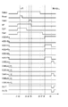
(全画素読み出しモード)
まず、加算動作を行わない動作モードについて図3を参照しながら説明する。ここでは全画素読み出しモードと称するが、画素アレイの全ての画素を読み出さなければならないわけではなく、画素間での加算処理を行わないことを意味するものとする。
(All-pixel readout mode)
First, an operation mode in which the addition operation is not performed will be described with reference to FIG. Although referred to herein as an all-pixel readout mode, it does not mean that all the pixels in the pixel array must be read out, and means that no addition processing is performed between the pixels.
時刻t1に、信号Select(n)がハイレベルになる。これによってn行目の画素に含まれる選択トランジスタ105がオンしてソースフォロワ動作を行うので、増幅トランジスタ103のゲート電極の電位、すなわちFD106の電位に対応したレベルが第1の垂直信号線130に現れる。すなわち、時刻t1に、n行目の画素が選択された状態が開始する。同じく時刻t1には、信号SPおよびCLPがハイレベルになるので、クランプ容量210には第1の垂直信号線に現れたレベルと電圧とCPDCとの電位差が与えられた状態となる。
At time t1, the signal Select (n) becomes high level. As a result, the
時刻t2から信号Reset(n)がパルス状にハイレベルになると、FD106の電位が電源電圧VDDに応じてリセットされる。これにより第1に垂直信号線130およびクランプ容量210の端子AにはFD部106をリセットしたことに対応するレベルが現れる。
When the signal Reset (n) becomes a high level in a pulse shape from time t2, the potential of the
時刻t3に信号CLPがローレベルになると、クランプスイッチ240が非導通状態になるので、第2の垂直信号線220が電気的に浮遊状態となる。これにより、クランプ容量210には、FD部106をリセットしたことに対応するレベルと電圧CPDCの電位差が保持される。
When the signal CLP becomes low level at the time t3, the
時刻t4に信号aRead(n)がハイレベルになると、フォトダイオード101に蓄積された電荷がFD部106へと転送される。転送された電荷量に応じてFD部106の電位が変化し、これに対応したレベルが第1の垂直信号線130に現れる。クランプ容量210には、FD部106をリセットしたことに対応するレベルと電圧CPDCとの電位差が保持されたままである。したがって、第2の垂直信号線220の電位は、FD部106をリセットしたことに対応するレベルと、フォトダイオード101からFD部106へと電荷を転送したことに対応するレベルとの差分ΔVinに容量で決まるゲインのかかった分だけ変動する。クランプ容量210の容量値をCcpとすると、第2の垂直信号線220に生じる電圧変化ΔVは、
ΔV = (Ccp・2・Csp)×ΔVin ・・・(1)
となる。
When the signal aRead (n) becomes a high level at time t4, the charge accumulated in the
ΔV = (Ccp · 2 · Csp) × ΔVin (1)
It becomes.
FD部106をリセットしたことに対応するレベルには、リセットトランジスタ104をスイッチングしたことによるノイズ成分や、画素を構成するトランジスタに固有のノイズ成分を含む。また、フォトダイオード101からFD部106に電荷を転送したことによるレベルにも、このノイズ成分が重畳されているので、クランプ容量210を用いて上述の動作を行うことでノイズを低減することができる。
The level corresponding to the reset of the
時刻t5に信号SPがローレベルになるとサンプルホールドスイッチ200が非導通になり、クランプ容量210と第1の垂直信号線130とは非導通状態になる。これによってΔVがサンプリング容量260−265に保持される。
When the signal SP becomes low level at time t5, the
時刻t6に信号Select(n)がローレベルになり、n行目の画素100に含まれる増幅トランジスタ103第1の垂直信号線130が非導通状態となることで、ソースフォロワ動作が終了する。つまり、n行目の画素が選択された状態が終了する。
At time t6, the signal Select (n) becomes low level, and the first
時刻t8に、ADDH1a、ADDH2a、およびADDH1bがハイレベルになる。このとき、図2の(a)、(b)より、各列に設けたサンプリング容量つまり、サンプリング容量260と261、サンプリング容量262と263、およびサンプリング容量264と265がそれぞれ並列で接続された状態で読み出される。
At time t8, ADDH1a, ADDH2a, and ADDH1b become high level. At this time, from FIGS. 2A and 2B, the sampling capacitors provided in each column, that is, the
時刻t9から信号CSEL(m)、CSEL(m+1)、・・・、CSEL(m+5)が順次供給されると、各列のサンプリング容量260−265に保持された信号が水平信号線280に出力される。サンプリング容量260−265に保持された信号を水平信号線280に出力するときには、容量の比で決まるゲインがかかる。水平線容量290の容量値をCcom、出力アンプ180のゲインをGampとすると、出力端子OUTに現れる出力Voutは、
Vout= ΔV x {Csp/(Csp+Ccom)} × Gamp
・・・(2)
となる。
When the signals CSEL (m), CSEL (m + 1),..., CSEL (m + 5) are sequentially supplied from time t9, the signals held in the
Vout = ΔV x {Csp / (Csp + Ccom)} × Gamp
... (2)
It becomes.
ダミースイッチを設けることで、サンプリング容量260−265の容量値が同一とみなせるため、上述の通りサンプリング容量の容量値をすべてCspとした。
Since the capacitance values of the
期間「n+1行」、「n+2行」以降も同様の動作が繰り返される。 The same operation is repeated after the period “n + 1 row” and “n + 2 row”.
(重み付け加算モード)
次に、水平方向に重み付けをして加算をする動作モードについて説明する。
(Weighted addition mode)
Next, an operation mode in which addition is performed by weighting in the horizontal direction will be described.
重み付け加算動作の説明に先立ち、重み付けをしない加算動作を説明する。図4(c)は、カラー光電変換装置において一般的に用いられる、ベイヤ配列のカラーフィルタの配列を示している。R、G、Bはそれぞれ赤、緑、青の色の光を透過させるフィルタである。このうち、n行目の配列を抜き出したものが図4(a)である。添え字は図の左側から数えた画素の位置を示し、( )で囲った数字は加算時の比率を示す。一般に、カラーフィルタを備えた光電変換装置において、行に沿った方向の加算を行う場合、同色の画素のうち隣接する画素からの信号を加算する。したがって、図4(a)においてG1とG3、R2とR4、G5とG7、R6とR8、・・・のような組み合わせで加算される。 Prior to the description of the weighted addition operation, the addition operation without weighting will be described. FIG. 4C shows an array of Bayer array color filters generally used in a color photoelectric conversion device. R, G, and B are filters that transmit red, green, and blue light, respectively. Among these, FIG. 4A shows an n-th row extracted. The subscript indicates the position of the pixel counted from the left side of the figure, and the number enclosed in () indicates the ratio at the time of addition. In general, when performing addition in a direction along a row in a photoelectric conversion device including a color filter, signals from adjacent pixels among pixels of the same color are added. Therefore, in FIG. 4A, addition is performed in combinations such as G1 and G3, R2 and R4, G5 and G7, R6 and R8,.
仮に、2つの画素の信号を1:1の比率で加算すると、G1とG3とを加算した後の信号の空間的な重心の位置はG1とG3の中間であるG2で示す位置となる。同様に、R2とR4はR3に、G5とG7はG6に、R6とR8はR7に、それぞれ加算後の信号の空間的な重心位置が現れる。したがって、光電変換装置の外部の映像信号処理回路等によって合成した画像のn行目の信号は、図4(a)の右側に示すような配置となる。つまり、加算後のGとRの空間的な位置は等ピッチにはならず、GとRとが近寄った偏心配置となる。このような色重心の偏心は、空間周波数の高い被写体を撮影した際に偽信号の原因となりうる。 If the signals of the two pixels are added at a ratio of 1: 1, the position of the spatial center of gravity of the signal after adding G1 and G3 becomes a position indicated by G2 which is between G1 and G3. Similarly, R2 and R4 appear in R3, G5 and G7 appear in G6, and R6 and R8 appear in R7, respectively. Therefore, the signals in the nth row of the image synthesized by the video signal processing circuit or the like outside the photoelectric conversion device are arranged as shown on the right side of FIG. In other words, the spatial positions of G and R after addition do not have equal pitches, but an eccentric arrangement in which G and R are close to each other. Such eccentricity of the color centroid can cause a false signal when a subject having a high spatial frequency is photographed.
このような偏心を改善するための手法が重み付け加算である。図4(b)を用いて重み付け加算の概念を説明する。重み付け加算においては、隣り合って設けられた3個のR画素を1:2:1の比率で加算する。すなわち、R2、R4、R6の画素であれば、1:2:1の比率で加算する。これにより、加算後のR画素の空間的な重心位置はR4で示す位置になる。同様にして、R6、R8、R10の画素を1:2:1の比率で加算する。一方、G画素については従来と同様に1:1の比率で加算する。したがって、出力端子OUTの後段に設けられた映像信号処理回路によって得られるn行目の信号は、図4(b)の右側に示すような配置になり、G画素とR画素とが互いに等ピッチに配列される。これにより、重み付けを行わない加算動作の場合に生じる偽信号が発生しにくくなるという利点がある。 A technique for improving such eccentricity is weighted addition. The concept of weighted addition will be described with reference to FIG. In the weighted addition, three adjacent R pixels are added at a ratio of 1: 2: 1. That is, if the pixels are R2, R4, and R6, they are added at a ratio of 1: 2: 1. Thereby, the spatial center-of-gravity position of the R pixel after the addition becomes a position indicated by R4. Similarly, R6, R8, and R10 pixels are added at a ratio of 1: 2: 1. On the other hand, G pixels are added at a ratio of 1: 1 as in the conventional case. Therefore, the n-th row signal obtained by the video signal processing circuit provided at the subsequent stage of the output terminal OUT is arranged as shown on the right side of FIG. 4B, and the G pixel and the R pixel are arranged at the same pitch. Arranged. Thereby, there is an advantage that a false signal generated in the case of the addition operation without weighting is hardly generated.
図5は、図1および2に示した光電変換装置における、重み付け加算モードの動作タイミングの例を示した図である。ここでは、図3で示した全画素読み出しモードにおける動作と異なる点を中心に説明する。全画素読み出しモードでは各列の備えたサンプリング容量のうち、260−261、262−263、および264−265を1組の容量として扱い、1画素からの信号を保持していた。これに対して、重み付け加算モードでは、サンプリング容量を二つに分割して利用する点で異なっている。 図2をもとに、信号処理部150a、150bの動作をそれぞれ説明する。図5に示したタイミング図において、信号ADDH2、ADDH3のタイミングが、全画素読み出しモードとは異なる。
FIG. 5 is a diagram illustrating an example of operation timing in the weighted addition mode in the photoelectric conversion device illustrated in FIGS. 1 and 2. Here, the description will focus on differences from the operation in the all-pixel readout mode shown in FIG. In the all-pixel readout mode, 260-261, 262-263, and 264-265 are handled as one set of sampling capacitors provided in each column, and signals from one pixel are held. On the other hand, the weighted addition mode is different in that the sampling capacity is divided into two. The operation of the
まず、信号処理部150aにおいては、隣接する2列の加算平均信号を出力する。時刻t8にADDH1、ADDH3がハイレベルとなり、加算スイッチ271、272、273、275、276が導通状態になる。サンプリング容量260、261、262、263が並列に接続されるため、信号が加算される。
First, the
その後、時刻t9にADDH3はローレベルになり、サンプリング容量260、261、262、263で保持された信号の平均値が保持される。つまり、(m)列と(m+2)列は1:1の割合で加算される。その後、時刻t10においてCSEL(m)がハイレベルになると、式(2)で示した回路ゲインにより、水平信号線280へと伝達される。
Thereafter, ADDH3 becomes low level at time t9, and the average value of the signals held by the
次に信号処理部150bの動作を説明する。時刻t8でADDHb1、ADDHb3がハイレベルとなり、加算スイッチ270、272、273、274、276が導通状態になる。サンプリング容量261、262、263、264が並列に接続されるため、信号が加算される。
Next, the operation of the
その後、時刻t9にADDH3はローレベルになり、サンプリング容量261、262、263、264で保持された信号の平均値が保持される。つまり、m+1列、(m+3)列、および(m+5)列の信号が1:2:1の割合で加算される。本例ではダミースイッチ251を設けることにより、サンプリング容量261、262、263、264の容量値が略同一になるよう調整をしているため、上述の1:2:1の割合での平均が精度よく実現できる。例えば、ダミースイッチ251がない場合には、スイッチの分寄生容量にずれが生じるため、スイッチ250の接合容量をΔCpとした場合、上述の加算において加算されるサンプリング容量の比は(C+ΔCp):(2xC+ΔCp):Cとなり、重み付けのバランスが1:2:1からくずれ、得られる画像の画質が低下する可能性がある。特に、素子の微細化などの理由からサンプリング容量260−265の値を大きく設定できない場合には、スイッチの接合容量を含めた寄生容量の影響が無視できなくなる。
Thereafter, ADDH3 becomes low level at time t9, and the average value of the signals held in the
その後、時刻t10においてCSEL(m+2)がハイレベルになると、式(2)で示した回路ゲインにより、水平信号線280へと伝達される。以後、同様の動作により順次読み出される。
Thereafter, when CSEL (m + 2) becomes high level at time t10, the signal is transmitted to the
以上の動作により、G画素とR画素と加算後の重心が互いに等ピッチに配列され、色重心のずれによる偽信号が発生しにくくなる。 With the above operation, the G pixel, the R pixel, and the added centroids are arranged at equal pitches, and a false signal due to a shift of the color centroid is less likely to occur.
上述の列選択スイッチ250とダミースイッチ251とは、ともにMOSトランジスタで構成することができる。このとき、両者のサイズを等しくすることで、第1および第2の容量に付随する容量値を一致させやすくなる。
Both the
なお、本実施例においては各列のサンプリング容量260−265の容量値の差を抑制する手段として、ダミースイッチを設けたが、ダミースイッチである必要はない。例えば、サンプリング262と263で容量値を(サンプリング容量262の容量値)<(サンプリング容量263の容量値)とすることで、読み出しスイッチ250の接合容量に相当する差分を抑制することもできる。すなわち、2つのサンプリング容量の容量値の差を低減するための容量調整部を設けることにより、重み付け加算を精度よく行うことができ、得られる画像から偽信号を低減することができる。容量調整部は、容量素子であってもよく、これ以降の実施例についても同様である。
In this embodiment, a dummy switch is provided as a means for suppressing the difference in the capacitance values of the
また、本実施例では水平信号容量290を増加させないために、ダミースイッチのソース端子とドレイン端子という主電極間をショートさせたが、例えば図6に示すよう1列分の等価回路の通り、ソースを固定電位に接続するなど、水平信号容量290を増加させない構成になっていればよい。
In this embodiment, in order not to increase the
(実施例2)
第1の実施例においては、画素に起因するノイズ成分を、信号処理部に含まれるクランプ容量を用いて低減するものを例示した。本発明に係る第2の実施例では画素に起因するノイズ成分を低減することに加えて、信号を増幅することができる構成を説明する。本実施例においても、第1の動作モードである全画素読み出しモードに加えて、第2の動作モードである重みつけ加算モードと、で動作できる光電変換装置を例にとって説明する。
(Example 2)
In the first embodiment, an example in which the noise component due to the pixel is reduced by using the clamp capacitor included in the signal processing unit is illustrated. In the second embodiment according to the present invention, a configuration capable of amplifying signals in addition to reducing noise components caused by pixels will be described. Also in the present embodiment, a photoelectric conversion apparatus that can operate in the weighted addition mode that is the second operation mode in addition to the all-pixel readout mode that is the first operation mode will be described as an example.
図7は、本実施例に係る信号処理部のうち1列分の回路を抜き出したものである。列増幅部Ampは、クランプ容量710、演算増幅部760、短絡スイッチ740およびフィードバック容量750を含む。クランプ容量710の一方の端子Aは第1の垂直信号線130に接続されており、他方の端子Bは演算増幅部760の反転入力端子に接続されるとともに、フィードバック容量780の一方の端子、および短絡スイッチ740の一方と接続されている。フィードバック容量750の他方の端子は、短絡スイッチ740の他方の電極および演算増幅器760の出力端子と接続される。演算増幅器760の非反転入力端子には基準電圧VC0Rが供給される。また、短絡スイッチは信号PC0Rによって制御される。信号PC0Rは、例えば不図示のタイミング制御回路部から供給される。列増幅部Ampのフィードバック容量を複数設けて、その接続を切り替えることで列増幅部Ampの増幅率を可変とすることができる。また、後述するが、クランプ容量710は、ノイズ低減部としても作用する。
FIG. 7 shows a circuit for one column extracted from the signal processing unit according to this embodiment. The column amplifier Amp includes a
演算増幅器760の出力端子、すなわち列増幅部Ampの出力端子は、スイッチ700、701を介してそれぞれサンプリング容量260s、261sおよびサンプリング容量260n、261nが接続されている。サンプリング容量にはさらにそれぞれ、加算制御スイッチ270s、270s、272sおよび270n、271n、272nが接続されており、列選択スイッチ250を介してそれぞれ水平信号線280s、nに接続される。水平信号線280s、280nは容量値Ccomを持つ。水平信号線容量は第1の水平信号線が持つ容量を模式的に表している。水平信号線280sは、出力部で差動増幅器790の非反転転端子、水平信号線280nは差動増幅器790反転入力端子に接続される。
サンプリング容量260s、261sは、それぞれ実施例1で説明した第1と第2の容量に対応する。同様に、サンプリング容量260n、261nは、それぞれ実施例1で説明した第1と第2の容量に対応する。これらのサンプリング容量は、スイッチ272を介して他の列のサンプリング容量のうち、第2または第1の容量に接続される。
The
図1における信号処理部150aと150bの両者が実質的に同じ構成であるため、両者を説明する図面として、図7がある。図7においては、信号ADDH1、ADDH2、ADDH3と示している。以下で説明するタイミング図では、信号処理部150aであればADDH1a、ADDH2a、ADDH3aが与えられ、信号処理部150bであればADDH1b、ADDH2b、ADDH3bが与えられるものとする。これは、本実施例以降の実施例についても同様である。
Since both the
(全画素読み出しモード)
次に図8を参照にしながら全画素読み出しモードの動作を説明する。なお、第1の垂直信号線130に接続される画素領域は、図1に示したものと同様であるとする。
(All-pixel readout mode)
Next, the operation in the all-pixel readout mode will be described with reference to FIG. Note that the pixel region connected to the first
時刻t1に信号SSelect(n)がハイレベルになると、n行目の画素に含まれる選択トランジスタが導通状態となり、増幅トランジスタがソースフォロワ動作を行うので、増幅トランジスタのゲート電極の電位、すなわちFD部106の電位に対応したレベルが第1の垂直信号線に現れる。 When the signal SSelect (n) becomes high level at time t1, the selection transistor included in the pixel in the n-th row is turned on, and the amplification transistor performs the source follower operation. Therefore, the potential of the gate electrode of the amplification transistor, that is, the FD portion A level corresponding to the potential of 106 appears on the first vertical signal line.
時刻t2から信号RESET(n)がパルス状にハイレベルになると、FD部106の電位が電源電圧VDDに応じてリセットされる。これによって第1の垂直信号線およびクランプ容量の端子Aには、FD部106をリセットしたことに対応するレベルが現れる。時刻t3から信号PC0Rがパルス状にハイレベルになると、短絡スイッチ740によって、演算増幅器760の反転入力端子と出力端子とが短絡される。このとき、演算増幅器760の反転入力端子は、演算増幅器760の仮想接地によりVC0Rの電位になる。つまり、フィードバック容量750の両端がVC0Rにリセットされ、クランプ容量710の端子BもVC0Rになる。
When the signal RESET (n) becomes a high level in a pulse shape from time t2, the potential of the
時刻t3には信号SHSおよびSHNもハイレベルとなるので、このときの演算増幅器の出力によってサンプリング容量がリセットされる。そして、信号PC0Rがローレベルになるとクランプ容量の端子Bは電気的浮遊状態となるので、クランプ容量には、FD部106をリセットしたことに対応するレベルと電圧VC0Rとの電圧差が保持される。
At time t3, the signals SHS and SHN also become high level, so that the sampling capacitor is reset by the output of the operational amplifier at this time. When the signal PC0R becomes a low level, the terminal B of the clamp capacitor is in an electrically floating state. Therefore, the clamp capacitor holds a voltage difference between the level corresponding to the reset of the
時刻t4から信号SHNがパルス状にハイレベルになると、このときの列増幅部Ampの出力がサンプリング容量260n、261nに保持される。サンプリング容量260n、261nに保持される信号には、列増幅部Ampに起因するオフセット成分が含まれる。
When the signal SHN becomes a pulse-like high level from time t4, the output of the column amplifier Amp at this time is held in the
時刻t5から信号READ(n)がパルス状にハイレベルになると、フォトダイオード101に蓄積された電荷がFD部106へと転送される。転送された電荷量に応じてFD部106の電位が変化し、これに対応したレベルが第1の垂直信号線130に現れる。クランプ容量には、FD部106をリセットしたことに対応するレベルと電圧PC0Rとの電位差が保持されたままであるので、クランプ容量の端子Bの電位は、FD部106をリセットしたことに対応したレベルと、フォトダイオード101からFD部106へと電荷を転送したことに対応するレベルとの差分ΔVinだけ変化する。第1の実施形態と異なるのは、ΔVinに対してクランプ容量とフィードバック容量Cfの容量値の比で決まるゲインがかかることである。つまり、クランプ容量の容量値をC0、フィードバック容量Cfの容量値をCfとすると、列信号部Ampの出力AmpOUTは
AmpOUT = (C0/Cf)x ΔVin ・・・(3)
となる。FDをリセットしたことに対応するレベルには、リセットトランジスタ104をスイッチングしたことによるノイズ成分や、画素を構成するトランジスタに固有のノイズ成分を含む。したがって、クランプ容量を用いて上述の動作を行うことで画素に起因するノイズ成分を低減することができる。さらに、本実施形態によれば電圧変化ΔVinをC0/Cfのゲインで増幅することができる。
When the signal READ (n) becomes a high level in a pulse shape from time t5, the charge accumulated in the
It becomes. The level corresponding to the resetting of the FD includes a noise component caused by switching the
時刻t6から信号SHSがハイレベルになり、その後ローレベルになると式(3)で表される電圧をサンプリング容量に保持する。サンプリング容量に保持される信号には、列信号部Ampの出力オフセットが含まれる。 When the signal SHS becomes high level from time t6 and then becomes low level, the voltage expressed by the equation (3) is held in the sampling capacitor. The signal held in the sampling capacitor includes the output offset of the column signal section Amp.
時刻t7に信号SSelect(n)がローレベルとなり、n行目の画素100に含まれる増幅トランジスタ103と第1の垂直信号線130とが非導通状態となることで、ソースフォロワ動作が終了する。言い換えると、n行目の画素が選択された状態が終了する。
At time t7, the signal SSelect (n) becomes a low level, and the
時刻t7に加算制御スイッチがハイレベルとなり、各列のサンプリング容量が接続される。時刻t8から信号CSEL(m)、CSEL(m+1)が順次供給されると、サンプリング容量に保持された信号が水平信号線に出力される。サンプリング容量に保持される信号を水平信号線に出力するには、容量の比で決まるゲインがかかる。水平信号線の容量値をCComとすると、水平信号線に現れる電圧Vs1は
Vs1 = { Csp/(Csp+CCom)}x(C0/Cf)x ΔVin
・・・(4)
となる。同様に、サンプリングに保持された信号を水平信号線に出力されるとともに容量の比できまるゲインがかかる。水平信号線の容量値をCComとすると、水平信号線に現れる電圧Vn1は、
Vn1 = {Csp/(Csp+CCom)}x(C0/Cf)x VC0R
・・・(5)
となる。差動増幅器に入力されるVs1とVn1の差分が出力端子OUTから出力される。Vs1とVn1の両者には列増幅部Ampの出力オフセットが含まれるので、出力端子OUTからは列増幅部Ampの出力オフセットが低減された信号として出力される。
At time t7, the addition control switch becomes high level, and the sampling capacitors of each column are connected. When signals CSEL (m) and CSEL (m + 1) are sequentially supplied from time t8, the signal held in the sampling capacitor is output to the horizontal signal line. In order to output the signal held in the sampling capacitor to the horizontal signal line, a gain determined by the capacitance ratio is applied. When the capacitance value of the horizontal signal line is CCom, the voltage Vs1 appearing on the horizontal signal line is Vs1 = {Csp / (Csp + CCom)} x (C0 / Cf) xΔVin
... (4)
It becomes. Similarly, a signal held in sampling is output to the horizontal signal line, and a gain determined by a capacitance ratio is applied. When the capacitance value of the horizontal signal line is CCom, the voltage Vn1 appearing on the horizontal signal line is
Vn1 = {Csp / (Csp + CCom)} x (C0 / Cf) xVC0R
... (5)
It becomes. The difference between Vs1 and Vn1 input to the differential amplifier is output from the output terminal OUT. Since both Vs1 and Vn1 include the output offset of the column amplifier Amp, the signal is output from the output terminal OUT as a signal with a reduced output offset of the column amplifier Amp.
(重み付け加算モード)
次に重みつけ加算モードについて説明する。図9に重み付け加算モードの駆動パターンを示す。サンプリング容量への信号書き込みの動作は全画素読みモードと同様のため、省略する。ここでは、図8に示した全画素読み出しモードと異なる点を中心に説明する。全画素読み出しモードでは各列のサンプリング容量を二つを一つ容量として扱っていた。これに対して、重み付け加算モードでは、サンプリング容量をそれぞれ分割して利用する点で異なる。実施例1と同様に、全画素読みモードとの違いは加算平均期間の信号制御にある。サンプリング容量260s、261sより構成される信号経路、およびサンプリング容量260n、261nより構成される信号経路それぞれにおいて、実施例1の図5で示した動作と同様に加算平均動作、および信号出力を行う。
(Weighted addition mode)
Next, the weighted addition mode will be described. FIG. 9 shows a driving pattern in the weighted addition mode. Since the signal writing operation to the sampling capacitor is the same as in the all-pixel reading mode, the description is omitted. Here, the description will focus on differences from the all-pixel readout mode shown in FIG. In the all-pixel readout mode, two sampling capacities in each column are treated as one capacity. In contrast, the weighted addition mode is different in that the sampling capacity is divided and used. Similar to the first embodiment, the difference from the all-pixel reading mode is in the signal control during the averaging period. In each of the signal path configured by the
以上の本発明の構成によれば、読み出し回路でゲインをかけて出力することが可能になり、よりS/N比を向上させつつ、精度よく重み付け加算を実施することができる。 According to the configuration of the present invention described above, it is possible to output with gain applied by the readout circuit, and weighted addition can be performed with high accuracy while further improving the S / N ratio.
本実施例においても、ダミースイッチ251を設けることにより、サンプリング容量260s、261s、260n、261nの容量値が略同一になるよう調整をしている。尚、本実施例においても、サンプリング262と263で容量値を(サンプリング容量262の容量値)<(サンプリング容量263の容量値)とすることで、読み出しスイッチ250の接合容量に相当する差分を抑制することもできる。すなわち、2つのサンプリング容量の容量値の差を低減するための容量調整部を設けることにより、重み付け加算を精度よく行うことができ、得られる画像から偽信号を低減することができる。
Also in the present embodiment, the dummy switches 251 are provided so that the capacitance values of the
また、本実施例では水平信号容量290を増加させないために、ダミースイッチのソース−ドレインをショートさせたが、例えば図6に示すよう1列分の等価回路の通り、ソースを固定電位に接続するなど、水平信号容量290を増加させない構成になっていればよい。
In this embodiment, in order not to increase the
(第3実施例)
次に、本発明に係る第3実施例を説明する。第2の実施例と大きく異なるのは、信号処理部の構成である。本実施例に係る信号処理部は、第1及び第2の容量に加えて、第3の容量を有する。そして、第1の垂直信号線から供給された信号を前記第3の容量に信号を保持させる第1の工程と、第1の容量が保持した信号を信号線に出力する第2の工程が少なくとも一部を時間的に並行して行うことを特徴とする。本実施例によれば、垂直加算動作および、水平加算平均動作が可能となる。
(Third embodiment)
Next, a third embodiment according to the present invention will be described. A significant difference from the second embodiment is the configuration of the signal processing unit. The signal processing unit according to the present embodiment has a third capacitor in addition to the first and second capacitors. The first step of holding the signal supplied from the first vertical signal line in the third capacitor and the second step of outputting the signal held by the first capacitor to the signal line are at least It is characterized in that a part is performed in parallel in time. According to this embodiment, a vertical addition operation and a horizontal addition average operation are possible.
図10に本実施例における信号処理部の1列分の構成を示す。実施例2と異なる点は第1の保持部である第3の容量1010s、1011s、1012s、および1010n、1011n、1012nはそれぞれ互いに並列に設けられている。第3の保持容量と第1および第2の容量との間にはバッファ部である差動増幅器1040を備えている。
FIG. 10 shows the configuration of one column of the signal processing unit in the present embodiment. The difference from the second embodiment is that the
第3の容量1010s、1011s、1012s、および1010n、1011n、1012nの組はそれぞれ、一方の端子が互いに短絡されるとともに差動増幅器1040の反転入力端子に接続される。第3の容量の他方の端子は、それぞれスイッチ1051s、1052s、1053sおよび1051n、1052n、1053nを介して、共通のノード1060s、1060nに接続されている。さらに、1070s、1070nを介して、差動増幅器1040の出力端子に接続されている。
The
サンプリング容量260s、261sは、それぞれ実施例1で説明した第1と第2の容量に対応する。同様に、サンプリング容量260n、261nは、それぞれ実施例1で説明した第1と第2の容量に対応する。これらのサンプリング容量は、スイッチ272を介して他の列のサンプリング容量のうち、第2または第1の容量に接続される。
The
前述の式(2)に示したように、第1および第2の容量は、信号線260に伝達される信号に対するゲインを低減させないために、小さくすることが困難であるが、第3の容量はこの限りではない。したがって、第3の容量の容量値を、第1の容量の容量値よりも小さくすることができる。
As shown in the above equation (2), the first and second capacitors are difficult to reduce because the gain for the signal transmitted to the
(全画素読み出しモード)
図11に、全画素読み出しモード時の動作を説明するためのタイミング図を示す。第1の垂直信号線130と接続される画素領域は、図1に示したものと同様であるとする。
(All-pixel readout mode)
FIG. 11 is a timing chart for explaining the operation in the all-pixel readout mode. The pixel region connected to the first
時刻t1に信号SSelect(n)がハイレベルになると、n行目の画素に含まれる選択トランジスタが導通状態となり、ソースフォロワ動作を行うので、増幅トランジスタのゲート電極の電位すなわちFD部106の電位に対応したレベルが第1の垂直信号線に現れる。
When the signal SSelect (n) becomes high level at time t1, the selection transistor included in the pixel in the n-th row becomes conductive and performs a source follower operation. Therefore, the potential of the gate electrode of the amplification transistor, that is, the potential of the
時刻t2から信号RESET(n)がパルス状にハイレベルになると、FD部106の電位が電源電圧VDDに応じてリセットされる。これによって第1の垂直信号線およびクランプ容量の端子Aには、FD部106をリセットしたことに対応するレベルが現れる。
When the signal RESET (n) becomes a high level in a pulse shape from time t2, the potential of the
時刻t3から信号PC0Rがパルス上にハイレベルになると、短絡スイッチ740によって、演算増幅器760の反転入力端子と出力端子とが短絡される。このとき、演算増幅器760の反転入力端子は、演算増幅器760の仮想接地によりVC0Rの電位になる。つまり、フィードバック容量750の両端がVC0Rにリセットされ、クランプ容量710の端子BもVC0Rになる。時刻t3には信号SHS1、SHS2、SHS3およびSHN1、SHN2、SHN3もハイレベルとなるので、このときの演算増幅器の出力によってサンプリング容量はリセットされる。そして、信号PC0Rがローレベルになるとクランプ容量の端子Bは電気的浮遊状態となるので、クランプ容量には、FD部106をリセットしたことに対応するレベルと電圧VC0Rとの電圧差が保持される。
When the signal PC0R becomes high level on the pulse from time t3, the inverting input terminal and the output terminal of the
時刻t4から信号SHN1がパルス状にハイレベルになると、このときの列増幅部Ampの出力が第1の保持容量1010n、1011n、1012nに保持される。第1の保持容量1010n、1011n、1012nに保持される信号には、列増幅部Ampの出力オフセットが含まれる。時刻t5から信号READ(n)がパルス状にハイレベルになると、フォトダイオード101に蓄積された電荷がFD部106へと転送される。転送された電荷量に応じてFD部106の電位が変化し、これに対応したレベルが第1の垂直信号線130に現れる。クランプ容量には、FD部106をリセットしたことに対応するレベルと電圧PC0Rとの電位差が保持されたままであるので、クランプ容量の端子Bの電位は、FD部106をリセットしたことに対応したレベルと、フォトダイオード101からFD部106へと電荷を転送したことに対応するレベルとの差分ΔVinだけ変化する。実施例2で説明したとおり、
式(3)で表すことができる。
When the signal SHN1 becomes a high level in a pulse form from time t4, the output of the column amplifier Amp at this time is held in the
It can be expressed by equation (3).
時刻t6から信号SHS1がハイレベルになり、その後ローレベルになると式(3)で表される電圧を第1の保持容量1010sに保持する。第1の保持容量1010sに保持される信号には、列信号部Ampの出力オフセットが含まれる。
When the signal SHS1 becomes high level from time t6 and then becomes low level, the voltage expressed by the equation (3) is held in the first holding
時刻t7に信号SSelect(n)がローレベルとなり、n行目の画素100に含まれる増幅トランジスタ103と第1の垂直信号線130とが非導通状態となることで、ソースフォロワ動作が終了する。
At time t7, the signal SSelect (n) becomes a low level, and the
一方、時刻t1において信号FBがハイレベルになり、スイッチ1060s、1060nが導通状態になる。これにより、差動増幅器1040の反転入力端子と接続された第1の保持容量の電極の電位はVClAmpは差動増幅器1040の出力オフセットが重畳されたレベルとなる。
On the other hand, at time t1, the signal FB becomes high level, and the
時刻t8において信号FBがローレベルになり、信号FBOがハイレベルになる。その後時刻t9にて信号VADD1が、時刻t10にて信号SW2がハイレベルになる、差動増幅器1040の出力端子と第2の保持容量が電気的に接続された状態となる。この動作によって、差動増幅器1040の出力オフセットが除去された信号が差動増幅器1040の出力端子に現れる。時刻t12以降は実施例2と同様に、第2の保持容量から水平信号線へ信号が読み出される。
At time t8, the signal FB becomes low level and the signal FBO becomes high level. Thereafter, the signal VADD1 becomes high level at time t9 and the signal SW2 becomes high level at time t10, and the output terminal of the
一方で、時刻t15からは「n+1」行目の読出しが開始する。時刻t1から時刻t7で示した「n行」を行うことにより、「n行」目の信号を第2の保持容量から水平信号線へ読みだす動作の一部を、「n+1行」目の信号を第1の保持容量に保持する動作が並行して行われる。 On the other hand, reading of the “n + 1” th row starts from time t15. By performing the “n-th row” shown from the time t1 to the time t7, a part of the operation of reading the “n-th row” signal from the second storage capacitor to the horizontal signal line is changed to the “n + 1-th row” signal. Are stored in the first storage capacitor in parallel.
本実施例によれば、画素からの信号を第1の保持容量に保持させる第1の工程、および第2の保持容量に保持された信号を水平出力線に出力する第2の工程の少なくとも一部が重複して行われることで、信号出力ない期間が時刻t8から時刻t13までとなり、画素信号の読出し速度を向上させることができる。 According to this embodiment, at least one of the first step of holding the signal from the pixel in the first holding capacitor and the second step of outputting the signal held in the second holding capacitor to the horizontal output line. Since the portions are overlapped, the period in which no signal is output is from time t8 to time t13, and the reading speed of the pixel signal can be improved.
(重み付け加算モード)
次に図12のタイミング図を参照しながら、垂直3行加算モード、および重み付け加算モードについて説明する。
(Weighted addition mode)
Next, the vertical three-row addition mode and the weighted addition mode will be described with reference to the timing chart of FIG.
時刻t1に信号Selectがハイレベルになると、n行目の画素に含まれる選択トランジスタが導通状態となり、増幅トランジスタがソースフォロワ動作を行うので、増幅トランジスタのゲート電極の電位すなわちFD部106の電位に対応したレベルが第1の垂直信号線に現れる。
When the signal Select becomes high level at time t1, the selection transistor included in the pixel in the n-th row becomes conductive, and the amplification transistor performs the source follower operation. Therefore, the potential of the gate electrode of the amplification transistor, that is, the potential of the
時刻t2から信号RESETがパルス状にハイレベルになると、FD部106の電位が電源電圧VDDに応じてリセットされる。これによって第1の垂直信号線およびクランプ容量の端子Aには、FD部106をリセットしたことに対応するレベルが現れる。
When the signal RESET becomes a high level in a pulse shape from time t2, the potential of the
時刻t3から信号PC0Rがパルス上にハイレベルになると、短絡スイッチ740によって、演算増幅器760の反転入力端子と出力端子とが短絡される。このとき、演算増幅器760の反転入力端子は、演算増幅器760の仮想接地によりVC0Rの電位になる。つまり、フィードバック容量750の両端がVC0Rにリセットされ、クランプ容量710の端子BもVC0Rになる。時刻t3には信号SHS1、SHS2、SHS3およびSHN1、SHN2、SHN3もハイレベルとなるので、このときの演算増幅器の出力によってサンプリング容量はリセットされる。そして、信号PC0Rがローレベルになるとクランプ容量の端子Bは電気的浮遊状態となるので、クランプ容量には、FD106をリセットしたことに対応するレベルと電圧VC0Rとの電圧差が保持される。
When the signal PC0R becomes high level on the pulse from time t3, the inverting input terminal and the output terminal of the
時刻t4から信号SHN1がパルス状にハイレベルになると、全画素読み出しモードで記載の通り、このときの列増幅部Ampの出力が第1の保持容量1010nに保持される。時刻t5から信号READ(n)がパルス状にハイレベルになると、フォトダイオード101に蓄積された電荷がFD106へと転送される。転送された電荷量に応じてFD106の電位が変化し、これに対応したレベルが第1の垂直信号線130に現れる。クランプ容量には、FD106をリセットしたことに対応するレベルと電圧PC0Rとの電位差が保持されたままであるので、クランプ容量の端子Bの電位は、FD106をリセットしたことに対応したレベルと、フォトダイオード101からFD106へと電荷を転送したことに対応するレベルとの差分ΔVinだけ変化する。実施例2で述べたとおり、列増幅部の出力は式(3)で表される。
When the signal SHN1 becomes a high level in a pulse form from time t4, the output of the column amplifier Amp at this time is held in the
時刻t6から信号SHS1がハイレベルになり、その後ローレベルになると式(3)で表される電圧をサンプリング容量1010sに保持する。
When the signal SHS1 becomes high level from time t6 and then becomes low level, the voltage expressed by the equation (3) is held in the
時刻t7にSSelectがパルス状にハイレベルになり、上述の動作を繰り返すことにより、サンプリング容量1011n、1011sにはそれぞれ、n+1行目の画素のリセット信号および光信号が保持される。
At time t7, SSelect becomes a high level in a pulse shape, and the above operation is repeated, whereby the reset signal and the optical signal of the pixel in the (n + 1) th row are held in the
時刻t8からは同様にn+2行目のリセット信号および、光信号が第1の保持容量1012n、1012sに保持される。
Similarly, from time t8, the reset signal and the optical signal in the (n + 2) th row are held in the
時刻t9において、信号FBがローレベルになり、信号FB0がハイレベルになる。 At time t9, the signal FB becomes low level and the signal FB0 becomes high level.
その後、時刻t10にて信号VADD1、VADD2、VADD3がハイレベルになると第1の保持容量の電極が電気的に保持されるので、第1の保持容量1010s、1011s、1012sおよび、1010n、1011n、1012nで保持されている3行分の信号がそれぞれ平均化される。また時刻t11にて、SW2がハイレベルになることで、第2の保持容量、260s、261sにはそれぞれ第1の保持容量1010s、1011s、1012sの平均化された信号が、260n、261nにはそれぞれ第1の保持容量1010n、1011n、1012nの平均化された信号が保持される。
After that, when the signals VADD1, VADD2, and VADD3 become high level at time t10, the electrodes of the first holding capacitors are electrically held, so that the
また、時刻t12では水平方向の画素信号の加算平均、時刻t13からは水平出力線への信号の読出しをそれぞれ実施例1で述べたものと同様の動作で実施する。一方、全画読出しモードと同様に、時刻t14では画素からの信号を第一の保持容量に保持させる第1の工程、および第2の保持容量に保持された信号を水平出力線に出力する第2の工程の少なくとも一部を時間的に並行して実施している。 Further, at time t12, the averaging of the pixel signals in the horizontal direction is performed, and from time t13, the signal reading to the horizontal output line is performed in the same manner as described in the first embodiment. On the other hand, as in the full image readout mode, at time t14, the first step of holding the signal from the pixel in the first holding capacitor, and the first step of outputting the signal held in the second holding capacitor to the horizontal output line. At least a part of the two steps is performed in parallel in time.
本実施例においても、ダミースイッチ251を設けることにより、サンプリング容量260s、261s、260n、261nの容量値が略同一になるよう調整をしている。尚、本実施例においても、サンプリング262と263で容量値を(サンプリング容量262の容量値)<(サンプリング容量263の容量値)とすることで、読み出しスイッチ250の接合容量に相当する差分を抑制することもできる。すなわち、2つのサンプリング容量の容量値の差を低減するための容量調整部を設けることにより、重み付け加算を精度よく行うことができ、得られる画像から偽信号を低減することができる。
Also in the present embodiment, the dummy switches 251 are provided so that the capacitance values of the
また、本実施例では水平信号容量290を増加させないために、ダミースイッチのソース−ドレインをショートさせたが、例えば図6に示すよう1列分の等価回路の通り、ソースを固定電位に接続するなど、水平信号容量290を増加させない構成になっていればよい。
In this embodiment, in order not to increase the
本実施例によれば、垂直方向の平均化を第1の保持容量で行っており、ジャギーを抑制することができる。画素からの信号を第1の保持容量に保持させる第一の工程および、第2の保持容量に保持された信号を水平出力線に出力する第3の工程の少なくとも一部を並行して行う。これにより、同一列の複数の画素からの信号を加算しつつ信号を高速に読み出すことができるので、ジャギーを抑制しつつフレームレートを向上させることが可能となる。 According to the present embodiment, vertical averaging is performed with the first storage capacitor, and jaggies can be suppressed. At least a part of the first step of holding the signal from the pixel in the first holding capacitor and the third step of outputting the signal held in the second holding capacitor to the horizontal output line are performed in parallel. As a result, signals can be read at high speed while adding signals from a plurality of pixels in the same column, so that it is possible to improve the frame rate while suppressing jaggies.
(実施例4)
次に、本実施形態に係る撮像システムの概略を、図13を用いて説明する。
Example 4
Next, an outline of the imaging system according to the present embodiment will be described with reference to FIG.
撮像システム800は、例えば、光学部810、撮像装置1000、映像信号処理回路部830、記録・通信部840、タイミング制御回路部850、システムコントロール回路部860、および再生・表示部870を含む。撮像装置1000は、先述の各実施例で説明した光電変換装置が用いられる。ここでは、図1に示したタイミングジェネレータ106が、撮像装置ではなく、タイミング制御回路部850に含まれる場合を例示している。
The
レンズなどの光学系である光学部は810、被写体からの光を撮像装置1000の、複数の画素が2次元状に配列された画素アレイに結像させ、被写体の像を形成する。撮像装置1000は、タイミング制御回路部850からの信号に基づくタイミングで、画素部に結像された光に応じた信号を出力する。
An
撮像装置1000から出力された信号は、映像信号処理部である映像信号処理回路部830に入力され、映像信号処理回路部830が、プログラムなどによって定められた方法に従って、入力された電気信号に対してAD変換などの処理を行う。映像信号処理回路部での処理によって得られた信号は画像データとして記録・通信部840に送られる。記録・通信部840は、画像を形成するための信号を再生・表示部870に送り、再生・表示部870に動画や静止画像が再生・表示させる。記録通信部は、また、映像信号処理回路部830からの信号を受けて、システムコントロール回路部860とも通信を行うほか、不図示の記録媒体に、画像を形成するための信号を記録する動作も行う。
A signal output from the
システムコントロール回路部860は、撮像システムの動作を統括的に制御するものであり、光学部810、タイミング制御回路部850、記録・通信部840、および再生・表示部870の駆動を制御する。また、システムコントロール回路部860は、例えば記録媒体である不図示の記憶装置を備え、ここに撮像システムの動作を制御するのに必要なプログラムなどが記録される。また、システムコントロール回路部860は、例えばユーザの操作に応じて駆動モードを切り替える信号を撮像システム内で供給する。具体的な例としては、読み出す行やリセットする行の変更、電子ズームに伴う画角の変更や、電子防振に伴う画角のずらしなどである。
The system
タイミング制御回路部850は、制御部であるシステムコントロール回路部860による制御に基づいて撮像装置1000および映像信号処理回路部830の駆動タイミングを制御する。
The timing
映像信号処理回路部830は、先述の各実施例で説明した補正係数を保持し、撮像装置1000から出力された信号に対して補正処理を行う。
The video signal
以上で説明した各実施例は、本発明を説明するための例示的なものであって、本発明の技術的思想を逸脱しない範囲で様々に変更あるいは組み合わせることが可能である。 Each embodiment described above is an example for explaining the present invention, and can be variously changed or combined without departing from the technical idea of the present invention.
110 画素領域
150a、150b 信号処理部
251 ダミースイッチ
110
Claims (14)
各々が、前記行列の列に対応して設けられた複数の信号処理部と、
信号線と、
を有する光電変換装置であって、
前記複数の信号処理部の各々は、
対応する前記列の画素に基づく信号を保持する第1の容量と第2の容量と、
前記第1の容量と前記信号線とを電気的に接続するスイッチと、
前記第2の容量と電気的に接続された容量調整部を有し、
一の前記信号処理部が有する前記第1の容量および別の一の前記信号処理部が有する第2の容量を互いに並列に電気的に接続可能な接続部と、を備え、
前記容量調整部は、一方の主電極が前記第2の容量と電気的に接続され、他方の主電極が電源または前記一方の主電極に電気的に接続されたMOSトランジスタを有することを特徴とする光電変換装置。 A plurality of pixels arranged in a matrix;
A plurality of signal processing units each corresponding to a column of the matrix;
A signal line;
A photoelectric conversion device comprising:
Each of the plurality of signal processing units includes:
A first capacitor and a second capacitor for holding a signal based on the corresponding pixel in the column;
A switch for electrically connecting the first capacitor and the signal line;
A capacity adjustment unit electrically connected to the second capacity;
E Bei and one said signal processing unit electrically connectable in parallel to each other a second capacitor, wherein the first capacitor and the signal processing unit of another has to have a connection portion,
The capacitance adjusting unit includes a MOS transistor in which one main electrode is electrically connected to the second capacitor and the other main electrode is electrically connected to a power source or the one main electrode. A photoelectric conversion device.
前記画素に基づく信号を保持する第3の容量と、
前記第3の容量が保持した信号を前記第1または第2の容量に伝達するバッファ部と、をさらに有することを特徴とする請求項1から7のいずれかに記載の光電変換装置。 The signal processing unit
A third capacitor for holding a signal based on the pixel;
The photoelectric conversion device according to any one of claims 1 to 7, characterized by further comprising a buffer unit for transmitting a signal the third capacitor is held in the first or second capacitor.
ことを特徴とする請求項8に記載の光電変換装置。 9. The photoelectric conversion device according to claim 8 , wherein a capacitance value of the third capacitor is smaller than a capacitance value of the first capacitor.
一の前記画素に基づく信号を、前記第1の容量から前記信号線に伝達する動作と、
別の前記画素に基づく信号を、前記第3の容量に保持させる動作と、の少なくとも一部を並行して行う
ことを特徴とする請求項8または9に記載の光電変換装置。 Each of the plurality of columns includes a plurality of the pixels,
An operation of transmitting a signal based on one pixel from the first capacitor to the signal line;
A signal based on another of the pixel, the photoelectric conversion device according to claim 8 or 9, characterized in that in parallel operation and to be held in the third capacitor, at least part of the.
前記接続部により、異なる列の複数の前記画素に基づく信号を加算しない第2の動作モードと、で動作すること
を特徴とする請求項1から10のいずれかに記載の光電変換装置。 A first operation mode for adding signals based on the plurality of pixels in different columns by the connection unit;
The photoelectric conversion device according to any one of the connecting part, different from a second mode of operation without adding the signal based on a plurality of the pixel columns in claim 1, characterized in that the operation 10.
各々が、前記行列の列に対応して設けられた複数の信号処理部と、
信号線と、
を有する光電変換装置であって、
前記複数の信号処理部の各々は、
対応する前記列の画素に基づく信号を保持する第1の容量と第2の容量と、
前記第1の容量と前記信号線とを電気的に接続するスイッチと、
前記第2の容量と電気的に接続されたMOSトランジスタと、
一の前記信号処理部が有する前記第1の容量および別の一の前記信号処理部が有する第2の容量を互いに並列に電気的に接続可能な接続部と、を備え、
前記MOSトランジスタのソース端子およびドレイン端子が短絡されていること、
を特徴とする光電変換装置。 A plurality of pixels arranged in a matrix;
A plurality of signal processing units each corresponding to a column of the matrix;
A signal line;
A photoelectric conversion device comprising:
Each of the plurality of signal processing units includes:
A first capacitor and a second capacitor for holding a signal based on the corresponding pixel in the column;
A switch for electrically connecting the first capacitor and the signal line;
A MOS transistor electrically connected to the second capacitor;
A connection section capable of electrically connecting the first capacitor of one signal processing unit and the second capacitor of another signal processing unit in parallel with each other;
The source terminal and drain terminal of the MOS transistor are short-circuited;
A photoelectric conversion device characterized by the above.
前記複数の画素に像を形成する光学系と、
前記光電変換装置から出力された信号を処理して画像データを生成する映像信号処理部と、
をさらに備えたこと
を特徴とする撮像システム。 A photoelectric conversion device according to any one of claims 1 to 13 ,
An optical system for forming an image on the plurality of pixels;
A video signal processing unit that processes the signal output from the photoelectric conversion device to generate image data;
An imaging system characterized by further comprising:
Priority Applications (3)
| Application Number | Priority Date | Filing Date | Title |
|---|---|---|---|
| JP2012018413A JP5967955B2 (en) | 2012-01-31 | 2012-01-31 | Photoelectric conversion device and imaging system |
| US13/753,182 US9305946B2 (en) | 2012-01-31 | 2013-01-29 | Photoelectric conversion apparatus that maintains image quality and image pickup system |
| CN201310043409.7A CN103227906B (en) | 2012-01-31 | 2013-01-31 | Photoelectric conversion device and image picking system |
Applications Claiming Priority (1)
| Application Number | Priority Date | Filing Date | Title |
|---|---|---|---|
| JP2012018413A JP5967955B2 (en) | 2012-01-31 | 2012-01-31 | Photoelectric conversion device and imaging system |
Publications (3)
| Publication Number | Publication Date |
|---|---|
| JP2013157889A JP2013157889A (en) | 2013-08-15 |
| JP2013157889A5 JP2013157889A5 (en) | 2015-02-26 |
| JP5967955B2 true JP5967955B2 (en) | 2016-08-10 |
Family
ID=48838146
Family Applications (1)
| Application Number | Title | Priority Date | Filing Date |
|---|---|---|---|
| JP2012018413A Expired - Fee Related JP5967955B2 (en) | 2012-01-31 | 2012-01-31 | Photoelectric conversion device and imaging system |
Country Status (3)
| Country | Link |
|---|---|
| US (1) | US9305946B2 (en) |
| JP (1) | JP5967955B2 (en) |
| CN (1) | CN103227906B (en) |
Families Citing this family (8)
| Publication number | Priority date | Publication date | Assignee | Title |
|---|---|---|---|---|
| JP6239975B2 (en) * | 2013-12-27 | 2017-11-29 | キヤノン株式会社 | Solid-state imaging device and imaging system using the same |
| JP6368128B2 (en) * | 2014-04-10 | 2018-08-01 | キヤノン株式会社 | Imaging device and imaging apparatus |
| JP6562675B2 (en) * | 2015-03-26 | 2019-08-21 | キヤノン株式会社 | Photoelectric conversion device, imaging system, and driving method of photoelectric conversion device |
| JP6527035B2 (en) * | 2015-06-30 | 2019-06-05 | 浜松ホトニクス株式会社 | Solid-state imaging device |
| CN107277396B (en) * | 2016-03-30 | 2021-02-26 | 松下知识产权经营株式会社 | Image pickup apparatus |
| JP7353752B2 (en) | 2018-12-06 | 2023-10-02 | キヤノン株式会社 | Photoelectric conversion device and imaging system |
| US11082643B2 (en) | 2019-11-20 | 2021-08-03 | Waymo Llc | Systems and methods for binning light detectors |
| JP7606370B2 (en) * | 2021-03-10 | 2024-12-25 | キヤノン株式会社 | Photoelectric conversion device and method for controlling photoelectric conversion device |
Family Cites Families (13)
| Publication number | Priority date | Publication date | Assignee | Title |
|---|---|---|---|---|
| JP3437208B2 (en) * | 1993-03-15 | 2003-08-18 | キヤノン株式会社 | Signal processing device |
| US20050224842A1 (en) | 2002-06-12 | 2005-10-13 | Takayuki Toyama | Solid-state imaging device, method for driving dolid-state imaging device, imaging method, and imager |
| JP2005277709A (en) * | 2004-03-24 | 2005-10-06 | Renesas Technology Corp | Solid-state image pickup device |
| JP4290066B2 (en) * | 2004-05-20 | 2009-07-01 | キヤノン株式会社 | Solid-state imaging device and imaging system |
| JP4349310B2 (en) * | 2004-12-27 | 2009-10-21 | ソニー株式会社 | Solid-state imaging device driving method, solid-state imaging device, and imaging apparatus |
| JP4416668B2 (en) | 2005-01-14 | 2010-02-17 | キヤノン株式会社 | Solid-state imaging device, control method thereof, and camera |
| JP4921911B2 (en) * | 2006-09-29 | 2012-04-25 | オリンパス株式会社 | Solid-state imaging device |
| JP2009141631A (en) * | 2007-12-05 | 2009-06-25 | Canon Inc | Photoelectric conversion device and imaging device |
| JP5151507B2 (en) * | 2008-01-29 | 2013-02-27 | ソニー株式会社 | Solid-state imaging device, signal readout method of solid-state imaging device, and imaging apparatus |
| JP5173503B2 (en) | 2008-03-14 | 2013-04-03 | キヤノン株式会社 | Imaging apparatus and imaging system |
| JP5161676B2 (en) | 2008-07-07 | 2013-03-13 | キヤノン株式会社 | Imaging apparatus and imaging system |
| JP5288955B2 (en) * | 2008-09-09 | 2013-09-11 | キヤノン株式会社 | Solid-state imaging device, imaging system, and driving method of solid-state imaging device |
| JP4891308B2 (en) | 2008-12-17 | 2012-03-07 | キヤノン株式会社 | Solid-state imaging device and imaging system using solid-state imaging device |
-
2012
- 2012-01-31 JP JP2012018413A patent/JP5967955B2/en not_active Expired - Fee Related
-
2013
- 2013-01-29 US US13/753,182 patent/US9305946B2/en not_active Expired - Fee Related
- 2013-01-31 CN CN201310043409.7A patent/CN103227906B/en not_active Expired - Fee Related
Also Published As
| Publication number | Publication date |
|---|---|
| CN103227906A (en) | 2013-07-31 |
| JP2013157889A (en) | 2013-08-15 |
| CN103227906B (en) | 2016-04-13 |
| US20130193310A1 (en) | 2013-08-01 |
| US9305946B2 (en) | 2016-04-05 |
Similar Documents
| Publication | Publication Date | Title |
|---|---|---|
| JP5288955B2 (en) | Solid-state imaging device, imaging system, and driving method of solid-state imaging device | |
| JP5967955B2 (en) | Photoelectric conversion device and imaging system | |
| US8913166B2 (en) | Solid-state imaging apparatus | |
| JP6253272B2 (en) | Imaging apparatus, imaging system, signal processing method, program, and storage medium | |
| JP6011546B2 (en) | Imaging device and imaging apparatus | |
| JP4659868B2 (en) | Solid-state imaging device and imaging system | |
| CN102843526B (en) | Picture pick-up device and control method thereof | |
| US20130002916A1 (en) | Image sensing device and image sensing system | |
| US9313433B2 (en) | Solid-state imaging device and electronic camera | |
| CN102164252B (en) | Solid-state image pickup apparatus and driving method therefor | |
| JP7116599B2 (en) | Imaging device, semiconductor device and camera | |
| JP6634035B2 (en) | Imaging device and imaging device | |
| JP6445866B2 (en) | Imaging apparatus, imaging system, and driving method of imaging apparatus | |
| CN102625058B (en) | An imaging apparatus, an imaging system, and a driving method of an imaging apparatus | |
| US9001247B2 (en) | Imaging system and method for driving imaging system | |
| JP2017011346A (en) | Imaging apparatus and imaging system | |
| JP6060500B2 (en) | Image sensor | |
| JP5284521B2 (en) | Photoelectric conversion device, imaging system, and driving method of photoelectric conversion device | |
| JP5188641B2 (en) | Photoelectric conversion device and imaging device | |
| JP2014217012A (en) | Solid-state imaging element and imaging device |
Legal Events
| Date | Code | Title | Description |
|---|---|---|---|
| A521 | Request for written amendment filed |
Free format text: JAPANESE INTERMEDIATE CODE: A523 Effective date: 20150108 |
|
| A621 | Written request for application examination |
Free format text: JAPANESE INTERMEDIATE CODE: A621 Effective date: 20150108 |
|
| A977 | Report on retrieval |
Free format text: JAPANESE INTERMEDIATE CODE: A971007 Effective date: 20160122 |
|
| A131 | Notification of reasons for refusal |
Free format text: JAPANESE INTERMEDIATE CODE: A131 Effective date: 20160202 |
|
| A521 | Request for written amendment filed |
Free format text: JAPANESE INTERMEDIATE CODE: A523 Effective date: 20160309 |
|
| TRDD | Decision of grant or rejection written | ||
| A01 | Written decision to grant a patent or to grant a registration (utility model) |
Free format text: JAPANESE INTERMEDIATE CODE: A01 Effective date: 20160607 |
|
| A61 | First payment of annual fees (during grant procedure) |
Free format text: JAPANESE INTERMEDIATE CODE: A61 Effective date: 20160705 |
|
| R151 | Written notification of patent or utility model registration |
Ref document number: 5967955 Country of ref document: JP Free format text: JAPANESE INTERMEDIATE CODE: R151 |
|
| LAPS | Cancellation because of no payment of annual fees |