JP5954991B2 - Optoelectronics semiconductor components - Google Patents
Optoelectronics semiconductor components Download PDFInfo
- Publication number
- JP5954991B2 JP5954991B2 JP2011546655A JP2011546655A JP5954991B2 JP 5954991 B2 JP5954991 B2 JP 5954991B2 JP 2011546655 A JP2011546655 A JP 2011546655A JP 2011546655 A JP2011546655 A JP 2011546655A JP 5954991 B2 JP5954991 B2 JP 5954991B2
- Authority
- JP
- Japan
- Prior art keywords
- scattering
- semiconductor chip
- scattering element
- optoelectronic semiconductor
- component according
- Prior art date
- Legal status (The legal status is an assumption and is not a legal conclusion. Google has not performed a legal analysis and makes no representation as to the accuracy of the status listed.)
- Active
Links
- 239000004065 semiconductor Substances 0.000 title claims description 157
- 230000005693 optoelectronics Effects 0.000 title claims description 37
- 238000006243 chemical reaction Methods 0.000 claims description 84
- 239000011159 matrix material Substances 0.000 claims description 32
- 239000002245 particle Substances 0.000 claims description 28
- 238000000149 argon plasma sintering Methods 0.000 claims description 25
- 239000000463 material Substances 0.000 claims description 21
- 238000000034 method Methods 0.000 claims description 20
- 230000005855 radiation Effects 0.000 claims description 14
- 238000007650 screen-printing Methods 0.000 claims description 12
- 238000004519 manufacturing process Methods 0.000 claims description 6
- 239000000919 ceramic Substances 0.000 claims description 5
- 229910010293 ceramic material Inorganic materials 0.000 claims description 5
- 229910004298 SiO 2 Inorganic materials 0.000 claims description 2
- 229910010413 TiO 2 Inorganic materials 0.000 claims description 2
- 230000005670 electromagnetic radiation Effects 0.000 claims 2
- 239000000853 adhesive Substances 0.000 claims 1
- 230000001070 adhesive effect Effects 0.000 claims 1
- 230000015572 biosynthetic process Effects 0.000 claims 1
- 229920001296 polysiloxane Polymers 0.000 description 12
- 239000000470 constituent Substances 0.000 description 8
- 230000000694 effects Effects 0.000 description 7
- 239000004593 Epoxy Substances 0.000 description 6
- 230000003287 optical effect Effects 0.000 description 5
- TWNQGVIAIRXVLR-UHFFFAOYSA-N oxo(oxoalumanyloxy)alumane Chemical compound O=[Al]O[Al]=O TWNQGVIAIRXVLR-UHFFFAOYSA-N 0.000 description 4
- 238000009792 diffusion process Methods 0.000 description 3
- 239000000203 mixture Substances 0.000 description 3
- 230000008878 coupling Effects 0.000 description 2
- 238000010168 coupling process Methods 0.000 description 2
- 238000005859 coupling reaction Methods 0.000 description 2
- 229910052751 metal Inorganic materials 0.000 description 2
- 239000002184 metal Substances 0.000 description 2
- 229910018072 Al 2 O 3 Inorganic materials 0.000 description 1
- VYPSYNLAJGMNEJ-UHFFFAOYSA-N Silicium dioxide Chemical compound O=[Si]=O VYPSYNLAJGMNEJ-UHFFFAOYSA-N 0.000 description 1
- 238000004026 adhesive bonding Methods 0.000 description 1
- 239000006185 dispersion Substances 0.000 description 1
- 238000004049 embossing Methods 0.000 description 1
- 239000011344 liquid material Substances 0.000 description 1
- 238000004020 luminiscence type Methods 0.000 description 1
- 239000004033 plastic Substances 0.000 description 1
- 229920005989 resin Polymers 0.000 description 1
- 239000011347 resin Substances 0.000 description 1
- 229910052814 silicon oxide Inorganic materials 0.000 description 1
- 238000001228 spectrum Methods 0.000 description 1
- 238000004528 spin coating Methods 0.000 description 1
- 230000000087 stabilizing effect Effects 0.000 description 1
- 229920005992 thermoplastic resin Polymers 0.000 description 1
- 229920001187 thermosetting polymer Polymers 0.000 description 1
- 239000012780 transparent material Substances 0.000 description 1
- 239000011345 viscous material Substances 0.000 description 1
Images


Classifications
-
- H—ELECTRICITY
- H01—ELECTRIC ELEMENTS
- H01L—SEMICONDUCTOR DEVICES NOT COVERED BY CLASS H10
- H01L25/00—Assemblies consisting of a plurality of individual semiconductor or other solid state devices ; Multistep manufacturing processes thereof
- H01L25/03—Assemblies consisting of a plurality of individual semiconductor or other solid state devices ; Multistep manufacturing processes thereof all the devices being of a type provided for in the same subgroup of groups H01L27/00 - H01L33/00, or in a single subclass of H10K, H10N, e.g. assemblies of rectifier diodes
- H01L25/04—Assemblies consisting of a plurality of individual semiconductor or other solid state devices ; Multistep manufacturing processes thereof all the devices being of a type provided for in the same subgroup of groups H01L27/00 - H01L33/00, or in a single subclass of H10K, H10N, e.g. assemblies of rectifier diodes the devices not having separate containers
- H01L25/075—Assemblies consisting of a plurality of individual semiconductor or other solid state devices ; Multistep manufacturing processes thereof all the devices being of a type provided for in the same subgroup of groups H01L27/00 - H01L33/00, or in a single subclass of H10K, H10N, e.g. assemblies of rectifier diodes the devices not having separate containers the devices being of a type provided for in group H01L33/00
- H01L25/0753—Assemblies consisting of a plurality of individual semiconductor or other solid state devices ; Multistep manufacturing processes thereof all the devices being of a type provided for in the same subgroup of groups H01L27/00 - H01L33/00, or in a single subclass of H10K, H10N, e.g. assemblies of rectifier diodes the devices not having separate containers the devices being of a type provided for in group H01L33/00 the devices being arranged next to each other
-
- H—ELECTRICITY
- H01—ELECTRIC ELEMENTS
- H01L—SEMICONDUCTOR DEVICES NOT COVERED BY CLASS H10
- H01L33/00—Semiconductor devices having potential barriers specially adapted for light emission; Processes or apparatus specially adapted for the manufacture or treatment thereof or of parts thereof; Details thereof
-
- H—ELECTRICITY
- H01—ELECTRIC ELEMENTS
- H01L—SEMICONDUCTOR DEVICES NOT COVERED BY CLASS H10
- H01L2924/00—Indexing scheme for arrangements or methods for connecting or disconnecting semiconductor or solid-state bodies as covered by H01L24/00
- H01L2924/0001—Technical content checked by a classifier
- H01L2924/0002—Not covered by any one of groups H01L24/00, H01L24/00 and H01L2224/00
-
- H—ELECTRICITY
- H01—ELECTRIC ELEMENTS
- H01L—SEMICONDUCTOR DEVICES NOT COVERED BY CLASS H10
- H01L2933/00—Details relating to devices covered by the group H01L33/00 but not provided for in its subgroups
- H01L2933/0091—Scattering means in or on the semiconductor body or semiconductor body package
-
- H—ELECTRICITY
- H01—ELECTRIC ELEMENTS
- H01L—SEMICONDUCTOR DEVICES NOT COVERED BY CLASS H10
- H01L33/00—Semiconductor devices having potential barriers specially adapted for light emission; Processes or apparatus specially adapted for the manufacture or treatment thereof or of parts thereof; Details thereof
- H01L33/48—Semiconductor devices having potential barriers specially adapted for light emission; Processes or apparatus specially adapted for the manufacture or treatment thereof or of parts thereof; Details thereof characterised by the semiconductor body packages
- H01L33/50—Wavelength conversion elements
-
- H—ELECTRICITY
- H01—ELECTRIC ELEMENTS
- H01L—SEMICONDUCTOR DEVICES NOT COVERED BY CLASS H10
- H01L33/00—Semiconductor devices having potential barriers specially adapted for light emission; Processes or apparatus specially adapted for the manufacture or treatment thereof or of parts thereof; Details thereof
- H01L33/48—Semiconductor devices having potential barriers specially adapted for light emission; Processes or apparatus specially adapted for the manufacture or treatment thereof or of parts thereof; Details thereof characterised by the semiconductor body packages
- H01L33/58—Optical field-shaping elements
Landscapes
- Engineering & Computer Science (AREA)
- Microelectronics & Electronic Packaging (AREA)
- Power Engineering (AREA)
- Computer Hardware Design (AREA)
- Manufacturing & Machinery (AREA)
- Physics & Mathematics (AREA)
- Condensed Matter Physics & Semiconductors (AREA)
- General Physics & Mathematics (AREA)
- Led Device Packages (AREA)
- Solid State Image Pick-Up Elements (AREA)
- Light Receiving Elements (AREA)
Description
ここに記載されているのは、オプトエレクトロニクス半導体構成部材である。 Described herein are optoelectronic semiconductor components.
本願は、独国特許第10 2009 005 907.5号に優先権を主張するものであり、その開示内容は、参照によってここに取り込まれるものとする。 The present application claims priority from German Patent No. 10 2009 005 907.5, the disclosure of which is hereby incorporated by reference.
本発明の解決すべき課題は、構成部材にわたって均一に分散されたビーム放射を可能にし、またこれによってこの構成部材の外部の観察者に対して輝度の違いが目立たないようにすることである。 The problem to be solved by the present invention is to allow for uniformly distributed beam radiation across the component, and thus to make the difference in brightness inconspicuous for observers outside the component.
本発明の半導体構成部材の少なくとも1つの実施形態によれば、この構成部材には、例えばマトリクス状に配置されかつビームを放射する複数の半導体チップが含まれている。この半導体チップは、共通の支持体に載置されている。ここでの関連において「マトリクス状」とは、複数のビーム放射半導体チップが有利には行および列の形態で支持体に載置されていることである。ここでこの半導体チップは、必ずしも規則的なグリッドで支持体に配置される必要はない。 According to at least one embodiment of the semiconductor component of the present invention, the component includes a plurality of semiconductor chips arranged in a matrix and emitting a beam, for example. This semiconductor chip is placed on a common support. In this context, “matrix” means that a plurality of beam-emitting semiconductor chips are mounted on the support, preferably in the form of rows and columns. Here, the semiconductor chip does not necessarily have to be arranged on the support with a regular grid.
例えば、上記のマトリクス状に配置された半導体チップに中間スペースが形成される。言い換えると、この場合に上記の半導体チップは、互いに間隔が空けられて配置されるのである。上記の構成部材を上から見ると、上記の中間スペースは、それぞれ互いに隣り合う2つの半導体チップの側面と、また半導体チップ側を向いた支持体表面の側面とによって区切られているのである。 For example, an intermediate space is formed in the semiconductor chips arranged in the matrix. In other words, in this case, the above-described semiconductor chips are arranged so as to be spaced from each other. When the above component members are viewed from above, the intermediate space is divided by the side surfaces of two semiconductor chips adjacent to each other and the side surface of the support surface facing the semiconductor chip side.
上記のビーム放射半導体チップは、例えばルミネセンスダイオードチップとすることが可能である。ここでこれらのルミネセンスダイオードチップは、発光ダイオードまたはレーザダイオードとすることができ、これらは、紫外光から赤外光までの範囲のビームを放射する。上記のルミネセンスダイオードチップは、有利には電磁ビームのスペクトルの可視または紫外領域において光を発する。上記の共通の支持体は、プリント基板または支持フレーム(リードフレーム)とすることが可能である。上記の構成部材は、例えば、表面実装形とすることができる。上記の支持体は、熱硬化性樹脂材料または熱可塑性樹脂材料によって構成することができ、またはセラミック材料によって構成することもでき、またはこのような材料から構成することが可能である。マトリクス状に配置される複数のビーム放射半導体チップは、共通の支持体上に載置される。 The beam emitting semiconductor chip can be a luminescence diode chip, for example. Here, these luminescent diode chips can be light-emitting diodes or laser diodes, which emit a beam in the range from ultraviolet light to infrared light. Said luminescent diode chip advantageously emits light in the visible or ultraviolet region of the spectrum of the electromagnetic beam. The common support can be a printed circuit board or a support frame (lead frame). The above-mentioned constituent member can be a surface mount type, for example. The support described above can be composed of a thermosetting resin material or a thermoplastic resin material, or can be composed of a ceramic material, or can be composed of such a material. A plurality of beam emitting semiconductor chips arranged in a matrix are mounted on a common support.
上記の半導体構成部材の少なくとも1つの実施形態によれば、上記の半導体チップから放射される電磁ビームを変換するため、少なくとも1つの変換素子が少なくとも1つの半導体チップに後置されている。この少なくとも1つの変換素子は、半導体構成部材のビーム出射路に沿って上記の半導体チップに後置されている。このビーム出射路は、半導体チップによる放射から、上記の構成部材から電磁ビームが出力結合されるまでのビームの光路である。この少なくとも1つの変換素子により、1つの波長の光が別の1つの波長の光に変換される。例えば上記の少なくとも1つの変換素子により、少なくとも1つの半導体チップから1次放射される青色の光の一部分が黄色の光に変換され、この黄色の光を青色の光と混合として白色光にすることができる。すなわち、上記の少なくとも1つの変換素子は、上記の半導体構成素子の動作時に光コンバータの機能を有するのである。上記の少なくとも1つの変換素子は有利には、上記の少なくとも1つの半導体チップのビーム出射面に載置され、上記の少なくとも1つの半導体チップと直接接触接続している。これは、例えば上記の半導体チップに変換素子を接着することによって達成することができる。また上記の変換素子をスクリーン印刷によって半導体チップのビーム出射面に載置することも可能である。これによって有利にも、上記の半導体チップによって1次放射される電磁ビームをチップの近くで色変換することができる。しかしながら上記の少なくとも1つの変換素子が、間接的にだけ半導体チップと接触接続させることも可能である。このことが意味し得るのは、変換素子/半導体チップの境界面間にギャップが構成されて変換素子と半導体チップとが接触しないことである。このギャップは、例えば空気などの気体で充填することができる。 According to at least one embodiment of the semiconductor component described above, at least one conversion element is placed on the at least one semiconductor chip in order to convert the electromagnetic beam emitted from the semiconductor chip. The at least one conversion element is placed on the semiconductor chip along the beam emission path of the semiconductor component. This beam emission path is an optical path of the beam from the radiation by the semiconductor chip to the electromagnetic coupling of the electromagnetic beam from the above constituent members. The light of one wavelength is converted into light of another wavelength by the at least one conversion element. For example, a part of blue light primarily emitted from at least one semiconductor chip is converted into yellow light by the at least one conversion element, and the yellow light is mixed with blue light to form white light. Can do. That is, the at least one conversion element has a function of an optical converter when the semiconductor component operates. The at least one conversion element is advantageously mounted on the beam exit surface of the at least one semiconductor chip and is in direct contact connection with the at least one semiconductor chip. This can be achieved, for example, by adhering a conversion element to the semiconductor chip. It is also possible to place the conversion element on the beam emitting surface of the semiconductor chip by screen printing. This advantageously makes it possible to color-convert the electromagnetic beam primarily emitted by the semiconductor chip as described above. However, it is also possible for the at least one conversion element to be contacted with the semiconductor chip only indirectly. This may mean that a gap is formed between the interface between the conversion element / semiconductor chip and the conversion element does not contact the semiconductor chip. This gap can be filled with a gas, for example air.
上記の変換素子は、シリコーン、エポキシ、シリコーンとエポキシとの混合物または透明なセラミックから構成することができ、この中に変換材料の粒子を入れることができる。 The conversion element can be composed of silicone, epoxy, a mixture of silicone and epoxy, or a transparent ceramic, into which particles of conversion material can be placed.
例えば、各半導体チップにちょうど1つの変換素子を対応付ける。ここで可能であるのは、各半導体チップに1つの変換素子を一義的に対応付けることである。 For example, exactly one conversion element is associated with each semiconductor chip. Here, it is possible to uniquely associate one conversion element with each semiconductor chip.
上記の構成部材の少なくとも1つの実施形態によれば、オプトエレクトロニクス構成部材には、各半導体チップに従属する少なくとも1つの散乱素子が含まれており、この散乱素子により、上記の半導体チップから放射される電磁ビームが拡散して散乱する。この散乱素子は有利には、上記の少なくとも1つの変換素子と直接接触している。上記の散乱素子には、例えば、マトリクス材料が含まれており、この材料に付加的にビームを散乱させる粒子が入れられる。この場合、上記の半導体チップから放射される電磁ビームは、ビーム散乱性粒子(デフューザ粒子とも称される)において散乱する。また同様に可能であるのは、上記の散乱素子を、例えば透明な材料からなる粗面化した板として構成することである。上記の散乱素子の実施形態には少なくとも2つの選択肢がある。まず1つには、ちょうど1つの散乱素子をすべての半導体チップに従属させることができる。別の1つは、各半導体チップに専用の1散乱素子を従属させ、ひいては一義的に対応付けることができる。ここで実証することができたのは、半導体チップから放射される電磁ビームが散乱素子によって殊に均一化されるため、上記の構成部材の放射特性において不均一性が回避されかつ強度ピークが平坦化されることである。したがって有利にも外部の観察者に対する眩惑作用が回避され、これによって上記の構成部材のビーム出射面は有利にもその輝度が一層均一および一様に見えるのである。 According to at least one embodiment of the above component, the optoelectronic component includes at least one scattering element subordinate to each semiconductor chip, which is emitted from the semiconductor chip. The electromagnetic beam diffuses and scatters. This scattering element is preferably in direct contact with the at least one conversion element. The scattering element includes, for example, a matrix material, and particles that additionally scatter the beam are placed in this material. In this case, the electromagnetic beam emitted from the semiconductor chip is scattered by beam scattering particles (also referred to as diffuser particles). Similarly, it is possible to configure the scattering element as a roughened plate made of, for example, a transparent material. There are at least two options for the scattering element embodiments described above. For one thing, exactly one scattering element can be subordinate to all semiconductor chips. Another one is that a dedicated one scattering element is subordinated to each semiconductor chip, which can be uniquely associated. What can be demonstrated here is that the electromagnetic beam emitted from the semiconductor chip is particularly uniformed by the scattering element, so that non-uniformity is avoided in the radiation characteristics of the above components and the intensity peak is flat. It is to become. Therefore, the dazzling effect on the external observer is advantageously avoided, so that the brightness of the beam exit surface of the component is advantageously more uniform and uniform.
この関連において「放射特性」とは、半導体構成部材の光軸に対するずれに依存する強度および色などの光放射特性のことである。 In this connection, “radiation characteristics” refers to light emission characteristics such as intensity and color depending on the deviation of the semiconductor component from the optical axis.
上記の構成部材の光軸は、半導体チップ側を向いた構成部材の支持体表面に対して垂直に延材している。 The optical axis of the constituent member extends perpendicularly to the support surface of the constituent member facing the semiconductor chip side.
上記の構成部材のビーム出射面は、例えば、すべての散乱素子または変換素子の枠によって囲まれている面のことである。 The beam emission surface of the above-described component is, for example, a surface surrounded by the frame of all scattering elements or conversion elements.
上記のような散乱素子を入れることの別の利点は、外部から入射する外部光が拡散して散乱素子によって反射されるため、この拡散して反射される外部光と、上記の構成部材によって形成される電磁ビームとが重ならないことである。これによって結果的に得られる利点は、このような散乱素子より、すでに述べた作用の他に付加的に有色光のコントラストが増大することである。 Another advantage of including a scattering element as described above is that external light incident from the outside is diffused and reflected by the scattering element, and thus formed by the diffused and reflected external light and the above-described components. The electromagnetic beam is not overlapped. The resulting advantage of this is that the contrast of the colored light is increased in addition to the effects already described, over such scattering elements.
さらに上記の散乱素子および変換素子は有利には互いに直接接触接続している。すなわち、散乱素子/変換素子の境界面においてギャップも、中間スペースないしは中断も形成されないのである。有利にもこれによって可能になるのは、上記の変換素子によって放射されるかまたは変換素子によって伝達される電磁ビームが可能な限りに大量に上記の散乱素子によって捉えられ、拡散されて散乱されることである。例えばこれは、上記の散乱素子が変換素子の上に接着されるかまたはスクリーン印刷プロセスによって散乱素子が変換素子に被着されることによって行われる。 Furthermore, the scattering element and the conversion element are preferably in direct contact with each other. That is, no gaps or intermediate spaces or interruptions are formed at the scattering element / conversion element interface. This advantageously makes it possible to capture as much of the electromagnetic beam emitted by or transmitted by the conversion element as possible, scattered and scattered by the scattering element. That is. For example, this can be done by adhering the scattering element above the conversion element or by attaching the scattering element to the conversion element by a screen printing process.
少なくとも1つの実施形態によれば、上記のオプトエレクトロニクス半導体構成部材には、マトリクス状に配置された複数のビーム放射半導体チップが含まれており、ここでこの半導体チップは、共通の支持体に載置される。さらに上記のオプトエレクトロニクス半導体構成部材には、少なくとも1つの変換素子が含まれており、この変換素子は、半導体チップによって放射される電磁ビームを変換するためにこの少なくとも1つの半導体チップに従属している。さらに各半導体チップには、この半導体チップによって放射される電磁ビームを拡散して散乱させる散乱素子が従属しており、この散乱素子は、上記の変換素子と直接接触接続している。ここでこの散乱素子は、ただ1つの散乱素子とするかまたは複数の散乱素子とすることが可能である。 According to at least one embodiment, the optoelectronic semiconductor component includes a plurality of beam emitting semiconductor chips arranged in a matrix, wherein the semiconductor chips are mounted on a common support. Placed. The optoelectronic semiconductor component further includes at least one conversion element, the conversion element being subordinate to the at least one semiconductor chip for converting an electromagnetic beam emitted by the semiconductor chip. Yes. Further, each semiconductor chip has a scattering element that diffuses and scatters the electromagnetic beam emitted by the semiconductor chip. This scattering element is in direct contact connection with the conversion element. Here, the scattering element can be a single scattering element or a plurality of scattering elements.
ここで説明するオプトエレクトロニクス半導体構成部材のベースになっている知識は殊に、散乱素子が設けられていない場合、上記の構成部材のビーム出射面の外部の観察者に対し、中間スペースを通して、上記の構成部材の支持体が識別可能であり、またこれにより、この構成部材のビーム出射面を観察した際に輝度の違いが生じてしまうことである。 The knowledge on which the optoelectronic semiconductor component described here is based is particularly known in the absence of a scattering element for the observer outside the beam exit surface of the component through the intermediate space. It is possible to identify the support member of the component member, and this causes a difference in luminance when the beam emission surface of the component member is observed.
したがって外部の観察者に対し、上記の半導体チップが設けられている明るく発光する領域と、半導体チップ間の中間スペースである発光していない暗い領域とからなる不均一な放射像が生じてしまう。ここではこのような不均一な放射像を回避するため、ここで説明する構成部材では、散乱素子を各半導体チップに従属させているというアイデアを利用し、ここでは散乱素子と変換素子とが直接接触接続している。この場合に外部の観察者に対して構成部材の中間スペースが暗く見えるという問題は、上記の構成部材のビーム出射面を上から見ると、上記の暗く見える中間スペースに、上記の散乱素子によって拡散して散乱される電磁ビームが重ね合わされることによって解決される。したがって上記の構成部材のビーム出射面を観察すると、上記のように暗く見える中間スペースには少なくとも局所的に、中間スペースの領域の散乱素子によって拡散して散乱される電磁ビームが重なっているのである。 Therefore, a non-uniform radiation image consisting of a bright light-emitting area where the semiconductor chip is provided and a dark area where light is not emitted, which is an intermediate space between the semiconductor chips, is generated for an external observer. Here, in order to avoid such a non-uniform radiation image, the component described here uses the idea that the scattering element is subordinate to each semiconductor chip. Here, the scattering element and the conversion element are directly connected to each other. Contact connection. In this case, the problem that the intermediate space of the structural member looks dark to the external observer is that the scattering element diffuses into the dark intermediate space when the beam exit surface of the structural member is viewed from above. This is solved by superimposing the scattered electromagnetic beams. Therefore, when observing the beam emission surface of the above-described component member, the electromagnetic space that is diffused and scattered by the scattering elements in the intermediate space region overlaps at least locally in the intermediate space that looks dark as described above. .
このことにより、観察者に対し、ビーム放射構成部材が均一であるという印象を持たせることができ、ビーム出射面にわたる輝度の違いが低減される。ここでの関連において「輝度」とは、構成部材のビーム出射面の明るさに対する尺度であり、面積当たり光の強度によって定義される。これにより、上記の構成部材は、ビーム出射面から見ると、外部の観察者には輝度が均一であるように見えるのである。 This can give the viewer the impression that the beam radiation component is uniform and reduce the difference in brightness across the beam exit surface. In this context, “brightness” is a measure for the brightness of the beam exit surface of the component and is defined by the intensity of light per area. As a result, when viewed from the beam exit surface, the above-described structural members appear to have uniform brightness to an external observer.
有利にも上記の少なくとも1つの散乱素子を半導体チップに載置することによって眩惑作用が回避される。それは、上記の散乱素子により、半導体チップによって放射された電磁ビームが拡散されて散乱するからである。これによってこの構成部材の放射特性において不均一性および強度ピークを回避することができる。 Advantageously, the dazzling effect is avoided by placing the at least one scattering element on a semiconductor chip. This is because the electromagnetic beam emitted by the semiconductor chip is diffused and scattered by the scattering element. This avoids inhomogeneities and intensity peaks in the radiation characteristics of this component.
少なくとも1つの実施形態によれば、隣り合う半導体チップ間の側方の間隔は、1〜150μmであり、有利には10〜150μmである。すなわち、隣り合う2つのチップの2つの側面の間隔は、10〜150μmである。これにより、極めてコンパクトでありかつスペースを節約する半導体構成部材が可能になる。さらにこれにより、中間スペースが占めるスペースを可能なかぎりに小さく維持することができる。 According to at least one embodiment, the lateral spacing between adjacent semiconductor chips is 1 to 150 μm, preferably 10 to 150 μm. That is, the distance between two side surfaces of two adjacent chips is 10 to 150 μm. This allows a semiconductor component that is extremely compact and saves space. Furthermore, this makes it possible to keep the space occupied by the intermediate space as small as possible.
上記のオプトエレクトロニクス半導体構成部材の少なくとも1つの実施形態によれば、上記の少なくとも1つの散乱素子は、マトリクス材料によって構成され、このマトリクス材料にビーム散乱粒子(拡散粒子とも称される)が入れられる。このマトリクス材料は、シリコーン、エポキシまたはシリコーンおよびエポキシからなる混合物とすることができる。この散乱素子はまたセラミック材料によって構成することも可能である。このマトリクス材料にはビーム散乱粒子が入れられ、この粒子によってマトリクス材料に入射するビームが拡散されて散乱される。ここでこのマトリクス材料は有利には、半導体チップによって形成される電磁ビームに対して透明な材料とすることができ、これにより、構成部材から可能な限りに多くのビームが出力結合されることが保証される。 According to at least one embodiment of the optoelectronic semiconductor component, the at least one scattering element is constituted by a matrix material into which beam scattering particles (also referred to as diffusing particles) are placed. . The matrix material can be silicone, epoxy or a mixture of silicone and epoxy. The scattering element can also be composed of a ceramic material. Beam scattering particles are placed in the matrix material, and the beam incident on the matrix material is diffused and scattered by the particles. Here, the matrix material can advantageously be a material that is transparent to the electromagnetic beam formed by the semiconductor chip, so that as many beams as possible are coupled out of the component. Guaranteed.
上記のオプトエレクトロニクス半導体構成部材の少なくとも1つの実施形態によれば、少なくとも1つのビーム散乱粒子は、少なくとも酸化ケイ素(SiO2),ZrO2,TiO2および/またはAlxOyの材料からなるか、またはこれらの材料のうちの少なくとも1つを含む。例えば、酸化アルミニウムは、Al2O3とすることが可能である。上記のビーム散乱粒子は、半導体構成部材に入れる前に上記のマトリクス材料と混ぜ合わされる。有利にはこのビーム散乱粒子をマトリクス材料内に分散させて、ビーム散乱粒子の濃度が、硬化したマトリクス材料において均一になるようにする。有利には、硬化されて散乱素子になる上記のマトリクス材料によって上記の電磁ビームが等方的に散乱される。放射ビームが粒子において散乱することにより、色の均一性が改善され、また電磁ビームの強度が平坦化される。ここで「色均一性」とは、散乱素子のビーム出射面を通る空間的な放射についての色調の安定性のことである。 According to at least one embodiment of the optoelectronic semiconductor component described above, does the at least one beam scattering particle comprise at least a material of silicon oxide (SiO 2 ), ZrO 2 , TiO 2 and / or Al x O y ? Or at least one of these materials. For example, the aluminum oxide can be Al 2 O 3 . The beam scattering particles are mixed with the matrix material before entering the semiconductor component. The beam scattering particles are preferably dispersed in the matrix material so that the concentration of the beam scattering particles is uniform in the cured matrix material. Advantageously, the electromagnetic beam is scattered isotropically by the matrix material, which is cured to become a scattering element. Scattering of the radiation beam at the particles improves color uniformity and flattens the intensity of the electromagnetic beam. Here, “color uniformity” refers to the stability of color tone with respect to spatial radiation passing through the beam exit surface of the scattering element.
上記のオプトエレクトロニクス半導体構成部材の少なくとも1つの実施形態によれば、上記のマトリクス材料におけるビーム散乱粒子の濃度は、1重量%以上である。この濃度は、有利には5重量%以上である。ここで実証することができたのは、上記の散乱素子におけるビーム散乱粒子がこのような濃度以上になれば、半導体チップから放射される電磁ビームが上記の散乱素子によって拡散して散乱し、外部の観察者に対し、ビーム出射面に暗く見える中間スペースが目立たなくなるのである。 According to at least one embodiment of the optoelectronic semiconductor component, the concentration of beam scattering particles in the matrix material is 1% by weight or more. This concentration is advantageously greater than or equal to 5% by weight. It was proved here that when the beam scattering particle in the above scattering element exceeds the above concentration, the electromagnetic beam emitted from the semiconductor chip is diffused and scattered by the above scattering element, Therefore, an intermediate space that looks dark on the beam exit surface becomes inconspicuous.
上記の半導体構成部材の少なくとも1つの実施形態によれば、上記の少なくとも1つの散乱素子は、マトリクス材料から構成され、このマトリクス材料にマイクロ構造が入れられる。すなわち、上記のマイクロ構造は、例えば粗粒のマイクロ構造(粒子とも称される)形態でマトリクス材料に入れられるのである。有利には上記の粗粒状のマイクロ構造は、それを取り囲むマトリクス材料とは異なる屈折率を有しているため、上記の電磁ビームは、拡散して上記のマイクロ構造において散乱するかまたは光学的に屈折する。粗粒のマイクロ構造は、シリコーン、エポキシまたはシリコーンおよびエポキシからなる混合物から構成することが可能である。 According to at least one embodiment of the semiconductor component described above, the at least one scattering element is composed of a matrix material, and a microstructure is placed in the matrix material. That is, the above-mentioned microstructure is put into the matrix material in the form of, for example, a coarse-grained microstructure (also called a particle). Advantageously, the coarse-grained microstructure has a refractive index different from that of the surrounding matrix material, so that the electromagnetic beam is diffused and scattered in the microstructure or optically. Refract. The coarse-grained microstructure can be composed of silicone, epoxy or a mixture of silicone and epoxy.
上記の半導体構成部材の少なくとも1つの実施形態によれば、上記の少なくとも1つの散乱素子は、光を散乱するシートまたは光を散乱する小板である。すなわち、半導体構成部材のビーム出射路に沿って上記の光散乱シートまたは小板が上記の変換素子に直接続いており、半導体チップによって放射される電磁ビームが拡散して散乱するのである。例えば、上記の光散乱シートまたは小板は、半導体チップ側を向いた、変換素子の上側面に接着される。上記の変換素子および光散乱シートまたは小板は有利には、互いに直接に接触接続しており、また変換素子/シートないしは変換素子/小板との境界面に、ギャップも中断も形成されることがない。上記のシートの厚さは有利には10〜50μmであり、殊に有利には30μmである。上記の小板は有利には500μm〜1mmの厚さを有する。上記のシートまたは小板は、電磁ビームに対して透明な材料、例えばシリコーンによって構成され、硬化させてシートまたは小板にする前にこのシリコーンにビーム散乱粒子が入れられる。光散乱シートは有利には、5重量%以上のビーム散乱粒子濃度を有する。 According to at least one embodiment of the semiconductor component described above, the at least one scattering element is a sheet that scatters light or a platelet that scatters light. That is, the light scattering sheet or platelet directly follows the conversion element along the beam emission path of the semiconductor component, and the electromagnetic beam emitted by the semiconductor chip is diffused and scattered. For example, the above light scattering sheet or platelet is adhered to the upper side surface of the conversion element facing the semiconductor chip side. The conversion element and the light scattering sheet or platelet are preferably in direct contact with each other, and gaps and interruptions are formed at the interface between the conversion element / sheet or the conversion element / plate. There is no. The thickness of the sheet is preferably from 10 to 50 μm, particularly preferably 30 μm. The platelets preferably have a thickness of 500 μm to 1 mm. The sheet or platelet is composed of a material that is transparent to the electromagnetic beam, such as silicone, into which the beam scattering particles are placed prior to curing into a sheet or platelet. The light scattering sheet preferably has a beam scattering particle concentration of 5% by weight or more.
択一的には上記の光散乱小板をセラミック材料によって構成することも可能である。 Alternatively, the light scattering platelets can be made of a ceramic material.
ビーム散乱粒子をマトリクス材料に入れるのに加えてまたはこれとは択一的に上記のシートも小板も共にその外側表面に構造化部分、例えば粗面を有することができる。上記のシートまたは小板は、硬化の後、半導体チップ側を向いた変換素子の表面に接着することが可能である。また粘性のある材料を直接載置し、つぎに硬化させることも可能である。 In addition to or in addition to placing the beam scattering particles in the matrix material, both the above-described sheets and platelets can have a structured portion, for example a rough surface, on the outer surface thereof. The above sheet or platelet can be bonded to the surface of the conversion element facing the semiconductor chip side after curing. It is also possible to place a viscous material directly and then cure it.
少なくとも1つの実施形態によれば、各半導体チップにはちょうど1つの散乱素子が従属されており、この散乱素子は、半導体チップに対応付けられた変換素子を側方に向かって突き出ている。散乱素子は、接着、スクリーン印刷または類似のものにより、半導体チップ側を向いた、変換素子の上側面に載置される。有利には上記の散乱素子は、変換素子の側方に突き出ており、また半導体チップの側方にも突き出ている。散乱素子は、覆われていないすべて側面において少なくとも5μm以上かつ最大で75μmだけ半導体チップを突き出ている。上記の散乱素子をこのように構成することにより、半導体チップに載置される散乱素子相互のそれぞれの間隔を低減ないしは最小化することができる。電磁ビームが放射される際、半導体チップによって放射される電磁ビームは拡散して散乱される。 According to at least one embodiment, exactly one scattering element is subordinate to each semiconductor chip, which scatters laterally through the conversion element associated with the semiconductor chip. The scattering element is placed on the upper side of the conversion element facing the semiconductor chip by gluing, screen printing or the like. Advantageously, the scattering element protrudes laterally of the conversion element and also protrudes laterally of the semiconductor chip. The scattering element has a semiconductor chip protruding at least 5 μm and a maximum of 75 μm on all sides that are not covered. By configuring the above scattering element in this way, it is possible to reduce or minimize the distance between the scattering elements mounted on the semiconductor chip. When the electromagnetic beam is emitted, the electromagnetic beam emitted by the semiconductor chip is diffused and scattered.
有利には電磁ビームは、上記の散乱素子における光分散により、拡散によって散乱され、また散乱素子の領域からの電磁ビームも拡散によって散乱される。ここで光出力結合面を上から見ると、これらの散乱素子の領域によって少なくとも部分的に上記の中間スペースが覆われる。したがってビーム出射面では少なくとも部分的に上記の暗く見える中間スペースが電磁ビームによって覆われ、ここでこの電磁ビームは、散乱素子により、上記の中間スペースの領域にわたっても散乱される。これにより、構成部材のビーム出射面が注視される場合、外部の観察者に対し有利にも電磁ビームを放射する領域と、中間スペースとの間での輝度の違いが小さくなる。したがってビーム出射面は、輝度が一層均一および一様に見え、これにより、観察者に対し、ビーム出射面全体にわたって均一にビームを放射する構成部材の印象が生じるのである。 The electromagnetic beam is preferably scattered by diffusion due to light dispersion in the scattering element, and the electromagnetic beam from the area of the scattering element is also scattered by diffusion. Here, when the light output coupling surface is viewed from above, the intermediate space is at least partially covered by the regions of these scattering elements. The intermediate space which appears dark at least partially on the beam exit surface is therefore covered by an electromagnetic beam, which is scattered by the scattering element over the region of the intermediate space. Thereby, when the beam emission surface of a structural member is watched, the difference in the brightness between the region where the electromagnetic beam is radiated advantageously to the external observer and the intermediate space is reduced. The beam exit surface thus appears more uniform and uniform in brightness, which gives the observer the impression of a component that emits the beam uniformly over the entire beam exit surface.
少なくとも1つの実施形態によれば、上記の半導体チップにはちょうど1つの散乱素子が後置され、この散乱素子により、すべての半導体チップが覆われる。ここでこの散乱素子は、関連するビーム出射面を有する。例えば、上記の散乱素子は、シートまたはプレートとすることができ、これらは、半導体チップとは反対側の、変換素子の上側面全体に載置される。この実施形態において散乱素子は、半導体チップだけではなく、半導体チップ間の中間スペースも完全に覆う。有利には散乱素子が自立式であるようにする。すなわち、載置後にこの散乱素子が別の固定および安定化手段を必要としないようにするのである。この場合に有利には散乱素子は、この散乱素子によって中間スペースが覆われる領域においてその形状を維持するため、中断箇所、不均一性が構成されることも、類似のものが構成されることもない。したがって上記のような暗く見える中間スペースは有利にも電磁ビームによって完全に覆われる。ここでこの電磁ビームは、散乱素子により、上記の中間スペースの領域にわたっても散乱される。これにより、電磁ビームを放射する領域と、中間スペースの領域との間の輝度の違いがさらに低減される。ビーム出射面の外部の観察者にとっては、電磁ビームの放射は、さらに均一に、またビーム出射面全体にわたって一層一様に分散しているように見える。また有利にも外部の観察者に対する眩惑作用が低減される。それは、半導体チップから放射される電磁ビームは、上記の散乱素子によってその強度が平滑化されるである。またさらに、構成部材のビーム出射面全体にわたって色調が均一化されかつ安定化される。このような散乱素子は殊に、半導体チップが多い構成部材に有利である。それは、この場合に構成部材のビーム出射面の面積が大きくなり、構成部材のすでに述べた有利な発光特性だけではなく、この散乱素子が、例えばただ1つの方法ステップにおいて載置することができるからである。 According to at least one embodiment, exactly one scattering element is placed after the semiconductor chip, and this scattering element covers all the semiconductor chips. The scattering element here has an associated beam exit surface. For example, the scattering element can be a sheet or a plate, which is mounted on the entire upper surface of the conversion element, opposite the semiconductor chip. In this embodiment, the scattering element completely covers not only the semiconductor chip but also the intermediate space between the semiconductor chips. Advantageously, the scattering element is self-supporting. That is, the scattering element is not required to have a separate fixing and stabilizing means after placement. In this case, the scatter element preferably maintains its shape in the area covered by the scatter element so that it can be interrupted, non-uniform, or similar. Absent. The intermediate space which appears dark as described above is therefore advantageously completely covered by the electromagnetic beam. Here, this electromagnetic beam is scattered by the scattering element over the region of the intermediate space. This further reduces the difference in brightness between the region emitting the electromagnetic beam and the intermediate space region. To an observer outside the beam exit surface, the radiation of the electromagnetic beam appears to be more evenly distributed and more evenly distributed throughout the beam exit surface. Also, the dazzling effect on the external observer is advantageously reduced. That is, the intensity of the electromagnetic beam emitted from the semiconductor chip is smoothed by the scattering element. Furthermore, the color tone is made uniform and stabilized over the entire beam exit surface of the component. Such a scattering element is particularly advantageous for components having many semiconductor chips. This is because, in this case, the area of the beam exit surface of the component is increased and not only the previously mentioned advantageous light emission properties of the component, but also this scattering element can be mounted in a single method step, for example. It is.
さらに本発明ではオプトエレクトロニクス半導体素子の作製方法が提供される。この方法により、ここで説明する構成部材を作製することができる。すなわち、上記の構成部材に関連して示したすべての特徴は、この方法に対しても示されているのであり、またその逆が成り立つのである。 Furthermore, the present invention provides a method for producing an optoelectronic semiconductor device. By this method, the constituent members described here can be produced. That is, all the features shown in relation to the above components are also shown for this method and vice versa.
上記の方法の少なくとも1つの実施形態によれば、まず支持素子を準備する。この支持素子は、例えばシートとすることが可能である。 According to at least one embodiment of the above method, first a support element is provided. The support element can be a sheet, for example.
第2のステップでは、スクリーン印刷プロセスを用いて少なくとも1つの変換素子を上記の支持素子上に形成する。第1テンプレートを載置した後、スクリーン印刷プロセスを用いて少なくとも1つの変換素子の材料を、例えばドクタによって支持素子に載置する。載置の後、また場合によっては材料を硬化させた後、第1テンプレートを支持素子から除去する。上記の少なくとも1つの変換素子用の材料として、例えばシリコーンを有する層または透明なセラミック製の層とすることができ、この層に上記の変換粒子が入れられる。 In the second step, at least one conversion element is formed on the support element using a screen printing process. After placing the first template, the material of the at least one conversion element is placed on the support element, for example by a doctor, using a screen printing process. After mounting and possibly curing the material, the first template is removed from the support element. The material for the at least one conversion element can be, for example, a layer comprising silicone or a transparent ceramic layer, into which the conversion particles are placed.
第3のステップでは、上記の支持素子上に載置した第2テンプレートを使用し、第2のスクリーン印刷プロセスにより、少なくとも1つの変換素子の覆われていない外側面全体に、第2の層として少なくとも1つの散乱素子を載置する。この散乱素子により、変換素子の覆われていないすべての側面と、支持素子とは反対側にある上側面とが覆われる。上記の材料は、例えばドクタによって載置することでき、引き続いて硬化される。 In the third step, the second template placed on the support element is used, and the second screen printing process forms a second layer on the entire uncovered outer surface of the at least one conversion element. At least one scattering element is mounted. This scattering element covers all the uncovered side surfaces of the conversion element and the upper side surface opposite to the support element. The above material can be placed, for example, by a doctor and subsequently cured.
上記の少なくとも1つの変換素子と第2層とからなる結合体から支持層および第2テンプレートを剥がした後、この結合体を少なくとも1つのビーム放射半導体チップ上に被着する。 After the support layer and the second template are peeled off from the combined body composed of the at least one conversion element and the second layer, the combined body is deposited on at least one beam emitting semiconductor chip.
以下では、本発明で説明する構成部材ならびに本発明で説明する方法を実施例およびそれに対応する図面によって詳説する。 In the following, the components described in the present invention and the method described in the present invention will be described in detail with reference to examples and the corresponding drawings.
実施例および図面において、同じまたは機能が同じ構成部材にはそれぞれ同じ参照符号が付されている。図示した素子は、縮尺通りとみなすべきではなく、むしろ個々の素子は、わかり易くするために誇張して大きく示されていることがある。 In the embodiments and the drawings, the same reference numerals are assigned to the same or similar components. The illustrated elements should not be considered to scale, but rather the individual elements may be exaggerated and enlarged for clarity.
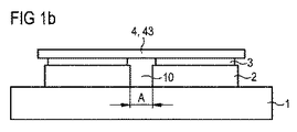
図1aにはここに説明する、支持体1を有するオプトエレクトロニクス半導体構成部材が概略断面図で示されている。マトリクス状に配置される半導体チップ2は、共通の支持体上に1に載置されている。 FIG. 1a shows a schematic cross-sectional view of an optoelectronic semiconductor component having a support 1 as described herein. The semiconductor chips 2 arranged in a matrix are mounted on a common support.
支持体1は、プラスチック、セラミックまたは金属によって構成することができる。支持体1は、プリント基板として構成され、または支持体1が金属製の場合にはこの構成部材の支持フレーム(リードフレーム)として構成される。 The support 1 can be made of plastic, ceramic or metal. The support 1 is configured as a printed circuit board, or is configured as a support frame (lead frame) of this component when the support 1 is made of metal.
半導体チップ2は、支持体1と導電的に接続されている。半導体チップ2の上には変換素子3が載置されており、この変換素子により、半導体チップ2から1次放射されたビームが、別の波長のビームに変換される。この実施例において変換素子3は、1つずつの光学CLC(Chip Level Conversion)層であり、この層により、半導体チップ2から1次放射された青色の光の一部が黄色の光に変換される。変換素子3はそれぞれ、シリコーンによって構成される層または透明なセラミック製の層とすることが可能であり、これに変換粒子が入れられる。
The
変換素子3にはそれぞれ、拡散された光を散乱させる散乱素子4が、光散乱小板41の形態で載置されており、この光散乱小板は、各半導体チップ2から側方に長さBだけ突き出ている。ここでは光散乱小板41は、それぞれ最大で75μmだけ半導体チップ2を突き出ている。光散乱小板41は、ここでは750μmの厚さを有する。光散乱小板41の材料はシリコーンであり、このシリコーンは、硬化させて小板4にする前に、酸化アルミニウムからなるビーム散乱粒子と混ぜ合わされる。光散乱小板41における酸化アルミニウムの濃度は、5重量%である。このような濃度によれば、構成部材のビーム出射面に沿った輝度の違いを最小化することについて、また外部の観察者に対して眩惑作用を回避することに極めて大きな効果を得ることできる。上記の構成部材のビーム出射面は、半導体チップ2側とは反対側を向いた光散乱小板41の上側面によって構成され、また決定される。さらにビーム出射面全体にわたって均一な色印象が得られるため、外部の観察者に対して、上記の構成部材は、あらかじめ設定可能な1つの色印象にしたがった見え方をするのである。半導体チップと半導体チップとの間の個々の側面の間隔は、Aによって決まり、また10〜150μmの範囲である。この実施例では、間隔Aは、100μmである。
Each of the
図1bには、散乱素子4が、関連する層によって構成されるオプトエレクトロニクス半導体構成部材が示されている。この実施例において層は、関連する光を散乱するシート43の形態の層である。光散乱シート43は、10〜50μmの厚さ、有利には30μmの厚さを有する。光散乱シート43はここでも、電磁ビームに対して透明なシリコーンによって構成され、硬化の前にこのシリコーンに濃度5重量%の酸化アルミニウム製のビーム散乱粒子が入れられている。光散乱シート43は、上記の構成部材を上から見ると、すべての半導体チップを覆い、また半導体チップ間の中間スペース10も完全に覆っている。有利にもこれにより光散乱シート43から中間スペース10の領域を介しても出射されかつ拡散によって散乱されるビームによって、暗く見える中間スペース10を覆うことができる。光散乱シート43には隙間がなくまたこの光散乱シートが、関連して層として構成されることにより、図1aに示した実施例の場合よりも、中間スペース10にはさらに完全にまた均一に、光散乱シート32によって散乱された電磁ビームが重ね合わせるかないしは中間スペースがこの電磁ビームによって覆われる。これによって有利にも回避されるのは、外部の観察者が、半導体チップ間の暗く見える中間スペース10を識別してこれに気づくことである。また有利にも、図1aの実施例についての説明で述べた別の所望の効果が得られる。このような散乱素子4は、多数の半導体チップ2を有する構成部材に対して殊に適している。それは、この場合にビーム出射面は面積が大きく、構成部材のすでに述べた有利な発光特性だけが得られるのではなく、光散乱シート43をただ1つの方法ステップにおいて被着することができるからである。したがって散乱素子4のこの実施形態により、コストが節約されるだけでなく、それを作製する時間も節約されるのである。
FIG. 1 b shows an optoelectronic semiconductor component in which the
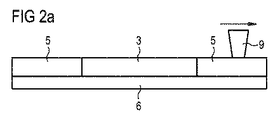
図2a,2b,2cおよび2dに関連し、概略断面図に基づいてここで説明する構成部材の作製方法を詳しく説明する。この構成部材は、例えば図1aの構成部材に相応する。図2aには、この作製プロセスに対する支持素子6として使用されるシートが示されている。支持素子6には第1テンプレート5が載置される。この実施例ではドクタ9である型押手段を用い、テンプレート5の開口部に変換素子3の材料を入れる。変換素子3の材料は、シリコーンを有する層またはセラミック材料からなる層とすることができ、この材料には変換粒子が入れられている。スクリーン印刷によってテンプレート5の上に変換素子3を載置しまた場合によって材料を硬化させた後、テンプレート5を支持素子6および変換素子3から除去する。変換素子3により、支持素子6上に第1の層が形成される。
In connection with FIGS. 2 a, 2 b, 2 c and 2 d, a method for producing the constituent members described here will be described in detail based on schematic sectional views. This component corresponds, for example, to the component of FIG. FIG. 2a shows a sheet used as
第2ステップでは第2の層7を支持素子6の上に載置し、また第2のスクリーンプロセスにより、ドクタ9を使用して第2テンプレート8上に散乱素子4を第2の層として被着する。第2の層7は、覆われていないすべての外側面において変換素子3を覆い、また変換素子3と直接接触接続する。これについては図2Bを参照されたい。変換素子3の上に第2の層7を載置した後、支持素子6からも、変換素子3および第2の層7からなる結合体からも第2テンプレート8を取り除く。ここでこの第2の層は、例えば変換層であり、この層により、変換素子3から放射される光が着色された光に変換される。
In the second step, the
第2変換層7aについては上記のプロセスを繰り返すことができ、また第3または別のステップにおいて上記の散乱素子が第2変換層7a上に載置される。
The process described above can be repeated for the
ここで説明したスクリーン印刷方式とは択一的に濃厚な液体状の材料をテンプレート5ないしは8上に滴下することができる。引き続いてスピンコーティングプロセスにより、支持素子6の表面に上記の材料を塗布してつぎに硬化させることができる。この結合体は続いて1つずつの半導体チップ2に載置される。この載置は、例えば、プレート搬送および/または接着によって行なうことが可能である。
As an alternative to the screen printing method described here, a thick liquid material can be dropped on the
また同様に可能であるのは、適当なテンプレートを使用し、個別の作製プロセスによって、マトリクス状に配置される多くの変換素子3を作製することであり、これは、例えばスクリーン印刷プロセスを用い、相応に得られるテンプレート5を使用して行われる。例えば第2のスクリーン印刷プロセスにより、板状の第2層が形成され、この層により、変換素子3の覆われていないすべての外側面が覆われて互いに関連させられる。支持素子6も第2テンプレート8も共に硬化させて除去した後、変換素子3と、変換素子3を包囲しかつこれに関連する第2層7とからなる板状の結合体が得られる。引き続いてこの板状の結合体を、マトリクス状に配置された半導体チップ2に直接載置することができる。この場合に上記の結合体は、上から見てすべての半導体チップ2のすべての構成部材およびこの構成部材の中間スペース10を覆う。有利にもこのようなプロセスは、殊にコスト的に有利である。
It is also possible to produce a number of
図3aには支持体1が概略平面図で示されており、この支持体上には半導体チップ2があり、また載置されている。半導体チップ2は、行および列の形態でマトリクス状に配置されている。
FIG. 3a shows a support 1 in a schematic plan view, on which a
図3bにはマトリクス状に配置された図3aの半導体チップが示されており、ここでは半導体チップ2上に個別の小板状の変換素子3が付加的に載置されている。それぞれの変換素子3に対応する1つずつの半導体チップへのこの変換素子の載置は、例えば、(ピックアンドプレースとも称される)プレート搬送および/または接着によって行うことができる。
FIG. 3 b shows the semiconductor chip of FIG. 3 a arranged in a matrix, in which individual small plate-
図3cには完成したオプトエレクトロニクス半導体構成部材が示されており、ここでは散乱素子4が、関連する層の形態で、例えば関連する光散乱シート43の形態で上記のマトリクス状に配置された半導体チップ2の上に載置されている。上から見ると半導体チップ2の表面もすべての中間スペース10も共に光散乱シート43によって覆われている。
FIG. 3c shows the completed optoelectronic semiconductor component, in which the
図3cに示した完成済のオプトエレクトロニクス半導体構成部材を線A−Aに沿い、側面図において観察すると、図1bに示したオプトエレクトロニクス半導体構成部材が得られる。 When the completed optoelectronic semiconductor component shown in FIG. 3c is observed in a side view along line AA, the optoelectronic semiconductor component shown in FIG. 1b is obtained.
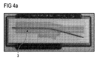
図4aにはスイッチオフされた動作状態にある上記のようなオプトエレクトロニクス半導体構成部材が概略平面図で示されている。ここからわかるのは、マトリクス状に配置された半導体チップ3およびやや明るく見える箇所であり、この箇所は、半導体チップ2上に載置された変換素子3を示している。
FIG. 4a shows a schematic plan view of such an optoelectronic semiconductor component in the switched-off operating state. What can be seen from this is the
図4bには、散乱素子が載置されていないオプトエレクトロニクス半導体構成部材がスイッチオンされた動作状態で示されている。明るく光る点は、外部の観察者が識別可能な半導体チップ2の放射面を示している。半導体チップ2の間にはそれぞれ中間スペース10があり、この中間スペースが暗く見えている。ここからわかるのは、半導体チップから中間スペースにかけて極めて大きな輝度の違いが生じることである。
In FIG. 4b, the optoelectronic semiconductor component on which no scattering element is mounted is shown in the switched-on operating state. The bright point indicates the radiation surface of the
図4cにはスイッチオンされた動作状態で本発明のオプトエレクトロニクス半導体構成部材が示されており、ここでは半導体チップ2上に、関連するシート43の形態の散乱素子4が載置にされている。この散乱素子4により、位置に依存する輝度の上記のような違いが均一化される。ここでもなお部分的に識別される明るく発光する点は、外部の観察者に識別可能な半導体チップ2の放射面である。散乱素子4を載置した後、中間スペース10はもはや識別することができないため、散乱素子4により、半導体チップから中間スペースにかけての半導体チップの輝度の違いを回避することができる。図4dおよび4eはこのようなオプトエレクトロニクス構成部材の平面図を示している。
FIG. 4 c shows the optoelectronic semiconductor component according to the invention in the switched-on operating state, in which a
図4dには散乱素子4のない構成部材が示されており、ここではマトリクス状に配置された半導体チップ2と、半導体チップ2上に載置された変換素子3とを識別することができる。グリッド状の暗い箇所は、この構成部材の中間スペース10である。
FIG. 4d shows a component without the
図4eは、完成したオプトエレクトロニクス構成部材の平面図を示しており、ここでは散乱素子4により、関連するシートが構成されており、このシートにより、すべての半導体チップおよびすべての中間スペース10が隙間なく覆われる。ここでは中間スペース10を識別することが格段に難しくなっている。
FIG. 4e shows a plan view of the completed optoelectronic component, in which the
本発明は、実施例に基づく上記の説明に限定されることはない。むしろ本発明にはあらゆる新規の特徴、ならびに殊に特許請求の範囲に示した特徴の任意の組み合わせを含む特徴のあらゆる組み合わせが含まれる。このことは、この特徴または組み合わせそのものが明示的に特許請求の範囲または実施例に示されていない場合であっても有効である。 The present invention is not limited to the above description based on the embodiments. Rather, the invention includes all novel features, and in particular any combination of features including any combination of the features recited in the claims. This is valid even if this feature or combination itself is not explicitly recited in the claims or examples.
Claims (12)
該オプトエレクトロニクス半導体構成素子は、
− ビームを放射し、かつ共通の支持体(1)に載置されている複数の半導体チップ(2)を有しており、
当該複数の半導体チップ(2)は、前記支持体(1)とは反対側を向いた1つずつのビーム出射面を有しており、
隣り合う2つの半導体チップ(2)の側方の間隔は10μmないし150μmの間であり、
前記オプトエレクトロニクス半導体構成素子はさらに、
− 前記複数の半導体チップ(2)から放射される電磁ビームを変換するために当該複数の半導体チップ(2)に従属する複数の変換素子(3)と、
− 前記の半導体チップ(2)から放射される電磁ビームを拡散させて散乱させるために各半導体チップ(2)に続く1つの散乱素子(4)とを有しており、
− 前記1つの散乱素子(4)は、すべての半導体チップ(2)を覆っており、前記1つの散乱素子(4)は、関連するビーム出射面を有しており、
− 前記1つの散乱素子(4)は、光散乱シート(43)または光散乱板(41)であり、
− 前記1つの散乱素子(4)は、前記複数の変換素子(3)と直接接触接続しており、
− 前記複数の変換素子(3)と前記1つの散乱素子(4)とは結合体を構成し、該結合体は、対応する前記の半導体チップ(2)に接着剤によって被着されているため、前記の各変換素子(3)は、一意に1つの半導体チップ(2)に対応付けられており、
− 前記複数の変換素子(3)は、対応する前記半導体チップ(2)の前記ビーム出射面だけを覆っているため、前記複数の変換素子(3)は、前記ビーム出射面と交差する方向に延在している、対応する前記半導体チップ(2)の側面を覆ってはおらず、
− 前記複数の変換素子(3)は、前記の対応する半導体チップ(2)のビーム出射面から側方にはみ出ていない、
ことを特徴とする、
オプトエレクトロニクス半導体構成素子。 In optoelectronic semiconductor components,
The optoelectronic semiconductor component is:
-Having a plurality of semiconductor chips (2) emitting a beam and mounted on a common support (1);
The plurality of semiconductor chips (2) have one beam exit surface facing the opposite side to the support (1),
The lateral distance between two adjacent semiconductor chips (2) is between 10 μm and 150 μm,
The optoelectronic semiconductor component further comprises:
- a plurality of transducers (3) subordinate to the plurality of semiconductor chips (2) to convert the electromagnetic radiation emitted from said plurality of semiconductor chips (2),
- has a connection Ku one scattering element (4) to the semiconductor chip (2) to scatter by diffusing electromagnetic radiation emitted from said semiconductor chip (2),
The one scattering element (4) covers all the semiconductor chips (2), the one scattering element (4) has an associated beam exit surface;
The one scattering element (4) is a light scattering sheet (43) or a light scattering plate (41);
The one scattering element (4) is in direct contact connection with the plurality of conversion elements (3);
- Configure the conjugate with the plurality of conversion elements (3) and before Symbol one scattering element (4), the conjugate is applied by an adhesive to a corresponding said semiconductor chip (2) Therefore, each of the conversion elements (3) is uniquely associated with one semiconductor chip (2),
- said plurality of converter elements (3), since covering only the radiation exit surface of the corresponding semiconductor chip (2), said plurality of conversion elements (3), in a direction intersecting with the beam exit surface Does not cover the corresponding side of the corresponding semiconductor chip (2),
The plurality of conversion elements (3) do not protrude laterally from the beam exit surface of the corresponding semiconductor chip (2);
It is characterized by
Optoelectronic semiconductor components.
請求項1に記載のオプトエレクトロニクス半導体構成素子。 The light scattering sheet (43) has a thickness of 10 to 50 μm,
The optoelectronic semiconductor component according to claim 1.
請求項1に記載のオプトエレクトロニクス半導体構成素子。 The light scattering plate (41) has a thickness of 500 μm to 1 mm.
The optoelectronic semiconductor component according to claim 1.
当該のマトリクス材料に前記のビーム散乱粒子が入れられている、
請求項1から3までのいずれか1項に記載のオプトエレクトロニクス半導体構成素子。 Before SL one scattering element (4) is constituted by a matrix material,
The beam scattering particles are contained in the matrix material;
The optoelectronic semiconductor component according to any one of claims 1 to 3.
SiO2,ZrO2,TiO2またはAlxOy
のうちの少なくとも1つから構成されるか、当該の材料のうちの1つを含む、
請求項4に記載のオプトエレクトロニクス半導体構成素子。 The at least one beam scattering particle is composed of the following materials: SiO 2 , ZrO 2 , TiO 2 or Al x O y.
Or comprises one of the materials of interest,
The optoelectronic semiconductor component according to claim 4.
請求項4または5に記載のオプトエレクトロニクス半導体構成素子。 The concentration of beam scattering particles in the matrix material is greater than 1% by weight,
The optoelectronic semiconductor component according to claim 4 or 5.
請求項1から6までのいずれか1項に記載のオプトエレクトロニクス半導体構成素子。 Before SL one scattering element (4) is composed of a matrix material microstructure has been introduced,
The optoelectronic semiconductor component according to any one of claims 1 to 6.
請求項1から7までのいずれか1項に記載のオプトエレクトロニクス半導体構成素子。 Before SL one scattering element (4) covers the all surfaces exposed semiconductor chip the conversion element which is not covered by (2) (3),
The optoelectronic semiconductor component according to any one of claims 1 to 7 .
請求項1から8までのいずれか1項に記載のオプトエレクトロニクス半導体構成素子。 Said scattering element (4) is self-supporting,
9. The optoelectronic semiconductor component according to any one of claims 1 to 8 .
請求項1から9までのいずれか1項に記載のオプトエレクトロニクス半導体構成素子。 The beam emitting semiconductor chip (2) is a light emitting diode chip or a laser diode chip.
Optoelectronic semiconductor component according to any one of claims 1 to 9.
前記1つの散乱素子(4)は、セラミック材料から構成されている、
請求項1から10までのいずれか1項に記載のオプトエレクトロニクス半導体構成素子。 Each of the plurality of conversion elements (3) is made of a transparent ceramic having particles of a conversion material,
Before SL one scattering element (4) is composed of ceramic material,
The optoelectronic semiconductor component according to any one of claims 1 to 10 .
− 第1スクリーン印刷プロセスを用いて前記の支持素子(6)に複数の変換素子(3)を構成するステップと、
− 第2スクリーン印刷プロセスを用いて前記複数の変換素子(3)の覆われていない外側面に1つの散乱素子(4)を構成して、前記複数の変換素子(3)と、前記1つの散乱素子(4)とから構成される結合体が形成されるようにするステップと、
− 当該結合体から前記の支持素子(6)を剥離するステップと、
− 引き続いて前記複数の変換素子(3)および前記1つの散乱素子(4)からなる結合体を複数のビーム放射半導体チップ(2)に載置するステップとを有することを特徴とする、
請求項1から11までのいずれか1項に記載のオプトエレクトロニクス半導体構成素子を作製する方法。 -Providing a support element (6);
-Forming a plurality of conversion elements (3) on said support element (6) using a first screen printing process;
- constitute one scattering element (4) on the outer surface uncovered with said plurality of transducer elements by using the second screen printing process (3), said plurality of conversion elements and (3), before Symbol 1 The formation of a combination comprising two scattering elements (4);
-Peeling said support element (6) from said combination;
- and having a step of placing the plurality of conversion elements (3) and said comprised of one scattering element (4) conjugate to a plurality of radiation-emitting semiconductor chip (2) Subsequently,
Method of making an optoelectronic semiconductor component according to any one of claims 1 to 11.
Applications Claiming Priority (3)
| Application Number | Priority Date | Filing Date | Title |
|---|---|---|---|
| DE102009005907.5 | 2009-01-23 | ||
| DE102009005907A DE102009005907A1 (en) | 2009-01-23 | 2009-01-23 | Optoelectronic semiconductor device |
| PCT/EP2009/067888 WO2010083929A1 (en) | 2009-01-23 | 2009-12-23 | Optoelectronic semiconductor component |
Publications (3)
| Publication Number | Publication Date |
|---|---|
| JP2012516044A JP2012516044A (en) | 2012-07-12 |
| JP2012516044A5 JP2012516044A5 (en) | 2012-12-27 |
| JP5954991B2 true JP5954991B2 (en) | 2016-07-20 |
Family
ID=41862160
Family Applications (1)
| Application Number | Title | Priority Date | Filing Date |
|---|---|---|---|
| JP2011546655A Active JP5954991B2 (en) | 2009-01-23 | 2009-12-23 | Optoelectronics semiconductor components |
Country Status (8)
| Country | Link |
|---|---|
| US (1) | US8916886B2 (en) |
| EP (1) | EP2382673B1 (en) |
| JP (1) | JP5954991B2 (en) |
| KR (1) | KR101647866B1 (en) |
| CN (1) | CN102292836B (en) |
| DE (1) | DE102009005907A1 (en) |
| TW (1) | TWI420647B (en) |
| WO (1) | WO2010083929A1 (en) |
Families Citing this family (28)
| Publication number | Priority date | Publication date | Assignee | Title |
|---|---|---|---|---|
| DE102010034915A1 (en) | 2010-08-20 | 2012-02-23 | Osram Opto Semiconductors Gmbh | Optoelectronic semiconductor component and scattering body |
| DE102011013369A1 (en) * | 2010-12-30 | 2012-07-05 | Osram Opto Semiconductors Gmbh | A method of manufacturing a plurality of semiconductor devices |
| DE102011050450A1 (en) | 2011-05-18 | 2012-11-22 | Osram Opto Semiconductors Gmbh | Optoelectronic semiconductor chip, optoelectronic semiconductor component and method for producing an optoelectronic semiconductor component |
| DE102011087614A1 (en) * | 2011-12-02 | 2013-06-06 | Osram Opto Semiconductors Gmbh | Optoelectronic arrangement for use in headlight in vehicle, has planar light conductor for mixing of electromagnetic radiation, arranged downstream to semiconductor chips in radiation pattern and covering gap between semiconductor chips |
| DE102012200973A1 (en) * | 2012-01-24 | 2013-07-25 | Osram Opto Semiconductors Gmbh | LIGHT AND METHOD FOR PRODUCING A LIGHT |
| DE102012101892B4 (en) * | 2012-03-06 | 2021-05-12 | OSRAM Opto Semiconductors Gesellschaft mit beschränkter Haftung | Wavelength conversion element, light-emitting semiconductor component and display device therewith as well as method for producing a wavelength conversion element |
| DE102012206970A1 (en) * | 2012-04-26 | 2013-10-31 | Osram Gmbh | Optical device for illumination device used in e.g. motor vehicle headlamp, has light scattering medium is constructed and arranged, such that it acts on light scattering from the first wavelength region light |
| JP5960565B2 (en) * | 2012-09-28 | 2016-08-02 | スタンレー電気株式会社 | Light emitting device for automobile headlamp and method for manufacturing the same |
| JP6093611B2 (en) * | 2013-03-18 | 2017-03-08 | スタンレー電気株式会社 | Light emitting device and manufacturing method thereof |
| DE102013207460A1 (en) * | 2013-04-24 | 2014-10-30 | Osram Opto Semiconductors Gmbh | Optoelectronic component |
| DE102013214877A1 (en) | 2013-07-30 | 2015-02-19 | Osram Opto Semiconductors Gmbh | Method for producing a cover element and an optoelectronic component, cover element and optoelectronic component |
| DE102013214896B4 (en) * | 2013-07-30 | 2021-09-09 | OSRAM Opto Semiconductors Gesellschaft mit beschränkter Haftung | Method for producing a converter element and an optoelectronic component, converter element and optoelectronic component |
| JP6694815B2 (en) | 2013-08-20 | 2020-05-20 | ルミレッズ ホールディング ベーフェー | Light emitting device |
| JP6079544B2 (en) * | 2013-10-07 | 2017-02-15 | 豊田合成株式会社 | Light emitting device and method for manufacturing light emitting device |
| US9499740B2 (en) | 2013-11-22 | 2016-11-22 | Nitto Denko Corporation | Light extraction element |
| DE102014102828A1 (en) * | 2014-03-04 | 2015-09-10 | Osram Opto Semiconductors Gmbh | Arrangement with a light-emitting diode |
| KR102424178B1 (en) * | 2014-09-02 | 2022-07-25 | 루미리즈 홀딩 비.브이. | Light source |
| DE102014112883A1 (en) * | 2014-09-08 | 2016-03-10 | Osram Opto Semiconductors Gmbh | Optoelectronic component |
| DE102014112973A1 (en) * | 2014-09-09 | 2016-03-10 | Osram Opto Semiconductors Gmbh | Optoelectronic component |
| JP6552190B2 (en) * | 2014-12-11 | 2019-07-31 | シチズン電子株式会社 | Light emitting device and method of manufacturing light emitting device |
| DE102015105474A1 (en) * | 2015-04-10 | 2016-10-13 | Osram Opto Semiconductors Gmbh | Converter component for an optoelectronic light-emitting device |
| DE102015106865A1 (en) * | 2015-05-04 | 2016-11-10 | Osram Opto Semiconductors Gmbh | Method for producing a converter component |
| JP6217705B2 (en) | 2015-07-28 | 2017-10-25 | 日亜化学工業株式会社 | Light emitting device and manufacturing method thereof |
| JP2017224867A (en) * | 2017-09-28 | 2017-12-21 | 日亜化学工業株式会社 | Light-emitting device and manufacturing method therefor |
| JP7083647B2 (en) | 2018-01-16 | 2022-06-13 | スタンレー電気株式会社 | Light emitting device |
| US11489005B2 (en) | 2019-12-13 | 2022-11-01 | Lumileds Llc | Segmented LED arrays with diffusing elements |
| US11680696B2 (en) | 2019-12-13 | 2023-06-20 | Lumileds Llc | Segmented LED arrays with diffusing elements |
| JP7531090B2 (en) | 2022-04-28 | 2024-08-09 | 日亜化学工業株式会社 | Light emitting device and light emitting module |
Family Cites Families (39)
| Publication number | Priority date | Publication date | Assignee | Title |
|---|---|---|---|---|
| JPS48102585A (en) * | 1972-04-04 | 1973-12-22 | ||
| JP3114805B2 (en) | 1998-04-15 | 2000-12-04 | 日亜化学工業株式会社 | Planar light source, display backlight using the same, and illuminated operation switch |
| JP4109756B2 (en) * | 1998-07-07 | 2008-07-02 | スタンレー電気株式会社 | Light emitting diode |
| DE19845229C1 (en) * | 1998-10-01 | 2000-03-09 | Wustlich Daniel | White light background lighting system, especially for flat displays, comprises blue-emitting LED chips and a diffuser foil with a coating containing a blue-to-white light conversion powder |
| US6271631B1 (en) | 1998-10-15 | 2001-08-07 | E.L. Specialists, Inc. | Alerting system using elastomeric EL lamp structure |
| GB2373368B (en) * | 2001-03-12 | 2004-10-27 | Arima Optoelectronics Corp | Light emitting devices |
| JP2003110146A (en) * | 2001-07-26 | 2003-04-11 | Matsushita Electric Works Ltd | Light-emitting device |
| JP2003191521A (en) * | 2001-12-26 | 2003-07-09 | Kyocera Corp | Method for assembling optical print head |
| WO2003098707A1 (en) | 2002-05-22 | 2003-11-27 | Applied Optotech Limited | Led array |
| JP4401681B2 (en) | 2003-05-19 | 2010-01-20 | 日東樹脂工業株式会社 | Light diffuser and optical member or optical device using the same |
| US7250715B2 (en) * | 2004-02-23 | 2007-07-31 | Philips Lumileds Lighting Company, Llc | Wavelength converted semiconductor light emitting devices |
| JP4360945B2 (en) | 2004-03-10 | 2009-11-11 | シチズン電子株式会社 | Lighting device |
| US7514867B2 (en) * | 2004-04-19 | 2009-04-07 | Panasonic Corporation | LED lamp provided with optical diffusion layer having increased thickness and method of manufacturing thereof |
| JP4667803B2 (en) * | 2004-09-14 | 2011-04-13 | 日亜化学工業株式会社 | Light emitting device |
| JP2006140362A (en) * | 2004-11-15 | 2006-06-01 | Nitto Denko Corp | Optical semiconductor device sealing sheet and optical semiconductor device manufacturing method using the same |
| US7344902B2 (en) * | 2004-11-15 | 2008-03-18 | Philips Lumileds Lighting Company, Llc | Overmolded lens over LED die |
| JP2006162846A (en) * | 2004-12-06 | 2006-06-22 | Asahi Glass Co Ltd | Diffusion plate for direct type backlight |
| US20060138938A1 (en) | 2004-12-27 | 2006-06-29 | Tan Kheng L | White LED utilizing organic dyes |
| US7564180B2 (en) * | 2005-01-10 | 2009-07-21 | Cree, Inc. | Light emission device and method utilizing multiple emitters and multiple phosphors |
| EP1862035B1 (en) * | 2005-03-14 | 2013-05-15 | Koninklijke Philips Electronics N.V. | Phosphor in polycrystalline ceramic structure and a light-emitting element comprising same |
| KR100593933B1 (en) | 2005-03-18 | 2006-06-30 | 삼성전기주식회사 | Side-emitting led package having scattering area and backlight apparatus incorporating the led lens |
| US7358543B2 (en) * | 2005-05-27 | 2008-04-15 | Avago Technologies Ecbu Ip (Singapore) Pte. Ltd. | Light emitting device having a layer of photonic crystals and a region of diffusing material and method for fabricating the device |
| JP2007067204A (en) * | 2005-08-31 | 2007-03-15 | Toshiba Lighting & Technology Corp | Light-emitting diode device |
| TWM289865U (en) * | 2005-11-08 | 2006-04-21 | Lighthouse Technology Co Ltd | Sectional light emitting diode backlight unit |
| JP4969119B2 (en) * | 2006-03-20 | 2012-07-04 | 日本碍子株式会社 | Light emitting diode device |
| DE102006024165A1 (en) | 2006-05-23 | 2007-11-29 | Patent-Treuhand-Gesellschaft für elektrische Glühlampen mbH | Optoelectronic semiconductor chip with a wavelength conversion substance and optoelectronic semiconductor component with such a semiconductor chip and method for producing the optoelectronic semiconductor chip |
| WO2008007232A2 (en) * | 2006-06-08 | 2008-01-17 | Koninklijke Philips Electronics N.V. | Light-emitting device |
| DE102007021009A1 (en) * | 2006-09-27 | 2008-04-10 | Osram Opto Semiconductors Gmbh | Light-emitting diode arrangement and method for producing such |
| DE102006051746A1 (en) | 2006-09-29 | 2008-04-03 | Osram Opto Semiconductors Gmbh | Optoelectronic component with a luminescence conversion layer |
| TWI338380B (en) * | 2006-10-11 | 2011-03-01 | Chuan Yu Hung | Light emitting diode incorporating high refractive index material |
| JP5392978B2 (en) * | 2006-10-30 | 2014-01-22 | 住友ベークライト株式会社 | Resin composition and semiconductor package manufactured using the resin composition |
| US20080121911A1 (en) * | 2006-11-28 | 2008-05-29 | Cree, Inc. | Optical preforms for solid state light emitting dice, and methods and systems for fabricating and assembling same |
| US7902560B2 (en) * | 2006-12-15 | 2011-03-08 | Koninklijke Philips Electronics N.V. | Tunable white point light source using a wavelength converting element |
| CN201137827Y (en) * | 2006-12-29 | 2008-10-22 | 东莞市科锐德数码光电科技有限公司 | High light amount LED fluorescent lamp |
| US9159888B2 (en) | 2007-01-22 | 2015-10-13 | Cree, Inc. | Wafer level phosphor coating method and devices fabricated utilizing method |
| US20080179618A1 (en) | 2007-01-26 | 2008-07-31 | Ching-Tai Cheng | Ceramic led package |
| JP5158472B2 (en) | 2007-05-24 | 2013-03-06 | スタンレー電気株式会社 | Semiconductor light emitting device |
| US8177382B2 (en) * | 2008-03-11 | 2012-05-15 | Cree, Inc. | Apparatus and methods for multiplanar optical diffusers and display panels for using the same |
| DE102008054029A1 (en) * | 2008-10-30 | 2010-05-06 | Osram Opto Semiconductors Gmbh | Optoelectronic semiconductor device |
-
2009
- 2009-01-23 DE DE102009005907A patent/DE102009005907A1/en not_active Withdrawn
- 2009-12-23 WO PCT/EP2009/067888 patent/WO2010083929A1/en active Application Filing
- 2009-12-23 JP JP2011546655A patent/JP5954991B2/en active Active
- 2009-12-23 EP EP09798937.0A patent/EP2382673B1/en active Active
- 2009-12-23 KR KR1020117019381A patent/KR101647866B1/en active IP Right Grant
- 2009-12-23 US US13/146,124 patent/US8916886B2/en active Active
- 2009-12-23 CN CN200980155142.2A patent/CN102292836B/en active Active
-
2010
- 2010-01-21 TW TW099101615A patent/TWI420647B/en not_active IP Right Cessation
Also Published As
| Publication number | Publication date |
|---|---|
| CN102292836B (en) | 2016-05-25 |
| US8916886B2 (en) | 2014-12-23 |
| US20120161162A1 (en) | 2012-06-28 |
| EP2382673B1 (en) | 2019-01-30 |
| KR101647866B1 (en) | 2016-08-11 |
| DE102009005907A1 (en) | 2010-07-29 |
| EP2382673A1 (en) | 2011-11-02 |
| JP2012516044A (en) | 2012-07-12 |
| TWI420647B (en) | 2013-12-21 |
| WO2010083929A1 (en) | 2010-07-29 |
| KR20110107384A (en) | 2011-09-30 |
| CN102292836A (en) | 2011-12-21 |
| TW201044549A (en) | 2010-12-16 |
Similar Documents
| Publication | Publication Date | Title |
|---|---|---|
| JP5954991B2 (en) | Optoelectronics semiconductor components | |
| US20110266576A1 (en) | Optoelectronic Semiconductor Component | |
| US9035339B2 (en) | Light emitting device and method | |
| KR101892593B1 (en) | A light emitting device and the manufacturing method | |
| JP5647028B2 (en) | Light emitting device and manufacturing method thereof | |
| US7315119B2 (en) | Light-emitting device having a phosphor particle layer with specific thickness | |
| US9576941B2 (en) | Light-emitting device and method of manufacturing the same | |
| JP4046118B2 (en) | LIGHT EMITTING ELEMENT, LIGHT EMITTING DEVICE USING SAME, AND SURFACE EMITTING LIGHTING DEVICE | |
| JP6099679B2 (en) | Beam emitting semiconductor element, lighting device and display device | |
| JP6215525B2 (en) | Semiconductor light emitting device | |
| JP5330306B2 (en) | Light emitting device | |
| US10424700B2 (en) | LED lamp sources, and the manufacturing methods and the backlight modules thereof | |
| JP6253949B2 (en) | LED light emitting device | |
| KR20110055744A (en) | Led with controlled angular non-uniformity | |
| US11106077B2 (en) | Light emitting module and method of manufacturing the same | |
| TWI733185B (en) | Surface light source module for backlight device and manufacturing method thereof | |
| JP2011114093A (en) | Lighting system | |
| JP2007207572A (en) | Light source device, back-light unit, and display device | |
| KR102428344B1 (en) | Optoelectronic component | |
| JP5450680B2 (en) | Semiconductor light emitting device | |
| JP6259329B2 (en) | LED light emitting device | |
| JP2012186337A (en) | Light-emitting device and manufacturing method thereof | |
| JP2004343149A (en) | Light emitting element and method of fabricating the same | |
| JP6189661B2 (en) | Semiconductor light emitting device | |
| JP2022513293A (en) | Optoelectronic lighting equipment and manufacturing method |
Legal Events
| Date | Code | Title | Description |
|---|---|---|---|
| A521 | Request for written amendment filed |
Free format text: JAPANESE INTERMEDIATE CODE: A523 Effective date: 20121106 |
|
| A621 | Written request for application examination |
Free format text: JAPANESE INTERMEDIATE CODE: A621 Effective date: 20121106 |
|
| A131 | Notification of reasons for refusal |
Free format text: JAPANESE INTERMEDIATE CODE: A131 Effective date: 20131125 |
|
| A601 | Written request for extension of time |
Free format text: JAPANESE INTERMEDIATE CODE: A601 Effective date: 20140224 |
|
| A602 | Written permission of extension of time |
Free format text: JAPANESE INTERMEDIATE CODE: A602 Effective date: 20140303 |
|
| A521 | Request for written amendment filed |
Free format text: JAPANESE INTERMEDIATE CODE: A523 Effective date: 20140324 |
|
| A131 | Notification of reasons for refusal |
Free format text: JAPANESE INTERMEDIATE CODE: A131 Effective date: 20140616 |
|
| A601 | Written request for extension of time |
Free format text: JAPANESE INTERMEDIATE CODE: A601 Effective date: 20140912 |
|
| A602 | Written permission of extension of time |
Free format text: JAPANESE INTERMEDIATE CODE: A602 Effective date: 20140922 |
|
| A521 | Request for written amendment filed |
Free format text: JAPANESE INTERMEDIATE CODE: A523 Effective date: 20141015 |
|
| A02 | Decision of refusal |
Free format text: JAPANESE INTERMEDIATE CODE: A02 Effective date: 20150216 |
|
| A521 | Request for written amendment filed |
Free format text: JAPANESE INTERMEDIATE CODE: A523 Effective date: 20150615 |
|
| A911 | Transfer to examiner for re-examination before appeal (zenchi) |
Free format text: JAPANESE INTERMEDIATE CODE: A911 Effective date: 20150622 |
|
| A912 | Re-examination (zenchi) completed and case transferred to appeal board |
Free format text: JAPANESE INTERMEDIATE CODE: A912 Effective date: 20150807 |
|
| A61 | First payment of annual fees (during grant procedure) |
Free format text: JAPANESE INTERMEDIATE CODE: A61 Effective date: 20160614 |
|
| R150 | Certificate of patent or registration of utility model |
Ref document number: 5954991 Country of ref document: JP Free format text: JAPANESE INTERMEDIATE CODE: R150 |
|
| R250 | Receipt of annual fees |
Free format text: JAPANESE INTERMEDIATE CODE: R250 |
|
| R250 | Receipt of annual fees |
Free format text: JAPANESE INTERMEDIATE CODE: R250 |
|
| R250 | Receipt of annual fees |
Free format text: JAPANESE INTERMEDIATE CODE: R250 |
|
| R250 | Receipt of annual fees |
Free format text: JAPANESE INTERMEDIATE CODE: R250 |
|
| R250 | Receipt of annual fees |
Free format text: JAPANESE INTERMEDIATE CODE: R250 |