JP5919723B2 - Display panel, display device and electronic device - Google Patents
Display panel, display device and electronic device Download PDFInfo
- Publication number
- JP5919723B2 JP5919723B2 JP2011229995A JP2011229995A JP5919723B2 JP 5919723 B2 JP5919723 B2 JP 5919723B2 JP 2011229995 A JP2011229995 A JP 2011229995A JP 2011229995 A JP2011229995 A JP 2011229995A JP 5919723 B2 JP5919723 B2 JP 5919723B2
- Authority
- JP
- Japan
- Prior art keywords
- anode electrode
- organic
- layer
- pixel
- hole injection
- Prior art date
- Legal status (The legal status is an assumption and is not a legal conclusion. Google has not performed a legal analysis and makes no representation as to the accuracy of the status listed.)
- Active
Links
- 239000010410 layer Substances 0.000 claims description 96
- 238000002347 injection Methods 0.000 claims description 51
- 239000007924 injection Substances 0.000 claims description 51
- 239000012044 organic layer Substances 0.000 claims description 35
- 230000005525 hole transport Effects 0.000 claims description 19
- 239000010409 thin film Substances 0.000 claims description 13
- 239000002184 metal Substances 0.000 claims description 8
- 229910052751 metal Inorganic materials 0.000 claims description 8
- 238000005215 recombination Methods 0.000 claims description 7
- 230000006798 recombination Effects 0.000 claims description 7
- 238000005401 electroluminescence Methods 0.000 description 48
- 239000000758 substrate Substances 0.000 description 14
- 238000005516 engineering process Methods 0.000 description 12
- 238000007740 vapor deposition Methods 0.000 description 10
- 239000003990 capacitor Substances 0.000 description 7
- 238000004519 manufacturing process Methods 0.000 description 7
- 238000000034 method Methods 0.000 description 6
- 239000011159 matrix material Substances 0.000 description 5
- 239000007769 metal material Substances 0.000 description 5
- 238000003860 storage Methods 0.000 description 5
- 238000009826 distribution Methods 0.000 description 4
- 239000000203 mixture Substances 0.000 description 4
- 230000004044 response Effects 0.000 description 4
- 230000007423 decrease Effects 0.000 description 3
- 238000000151 deposition Methods 0.000 description 3
- 239000000463 material Substances 0.000 description 3
- 230000004048 modification Effects 0.000 description 3
- 238000012986 modification Methods 0.000 description 3
- 230000015556 catabolic process Effects 0.000 description 2
- 238000006731 degradation reaction Methods 0.000 description 2
- 230000000694 effects Effects 0.000 description 2
- 239000011521 glass Substances 0.000 description 2
- 230000006872 improvement Effects 0.000 description 2
- 239000004973 liquid crystal related substance Substances 0.000 description 2
- 230000009467 reduction Effects 0.000 description 2
- 238000007789 sealing Methods 0.000 description 2
- 229910000838 Al alloy Inorganic materials 0.000 description 1
- 230000008859 change Effects 0.000 description 1
- 230000000052 comparative effect Effects 0.000 description 1
- 230000008021 deposition Effects 0.000 description 1
- 238000010586 diagram Methods 0.000 description 1
- 230000003287 optical effect Effects 0.000 description 1
- 150000002894 organic compounds Chemical class 0.000 description 1
Images


Classifications
-
- H—ELECTRICITY
- H10—SEMICONDUCTOR DEVICES; ELECTRIC SOLID-STATE DEVICES NOT OTHERWISE PROVIDED FOR
- H10K—ORGANIC ELECTRIC SOLID-STATE DEVICES
- H10K59/00—Integrated devices, or assemblies of multiple devices, comprising at least one organic light-emitting element covered by group H10K50/00
- H10K59/80—Constructional details
- H10K59/805—Electrodes
- H10K59/8051—Anodes
- H10K59/80515—Anodes characterised by their shape
-
- H—ELECTRICITY
- H10—SEMICONDUCTOR DEVICES; ELECTRIC SOLID-STATE DEVICES NOT OTHERWISE PROVIDED FOR
- H10K—ORGANIC ELECTRIC SOLID-STATE DEVICES
- H10K50/00—Organic light-emitting devices
- H10K50/80—Constructional details
- H10K50/805—Electrodes
- H10K50/81—Anodes
- H10K50/813—Anodes characterised by their shape
-
- H—ELECTRICITY
- H10—SEMICONDUCTOR DEVICES; ELECTRIC SOLID-STATE DEVICES NOT OTHERWISE PROVIDED FOR
- H10K—ORGANIC ELECTRIC SOLID-STATE DEVICES
- H10K2102/00—Constructional details relating to the organic devices covered by this subclass
- H10K2102/301—Details of OLEDs
- H10K2102/302—Details of OLEDs of OLED structures
-
- H—ELECTRICITY
- H10—SEMICONDUCTOR DEVICES; ELECTRIC SOLID-STATE DEVICES NOT OTHERWISE PROVIDED FOR
- H10K—ORGANIC ELECTRIC SOLID-STATE DEVICES
- H10K50/00—Organic light-emitting devices
- H10K50/10—OLEDs or polymer light-emitting diodes [PLED]
- H10K50/14—Carrier transporting layers
- H10K50/15—Hole transporting layers
-
- H—ELECTRICITY
- H10—SEMICONDUCTOR DEVICES; ELECTRIC SOLID-STATE DEVICES NOT OTHERWISE PROVIDED FOR
- H10K—ORGANIC ELECTRIC SOLID-STATE DEVICES
- H10K50/00—Organic light-emitting devices
- H10K50/10—OLEDs or polymer light-emitting diodes [PLED]
- H10K50/17—Carrier injection layers
-
- H—ELECTRICITY
- H10—SEMICONDUCTOR DEVICES; ELECTRIC SOLID-STATE DEVICES NOT OTHERWISE PROVIDED FOR
- H10K—ORGANIC ELECTRIC SOLID-STATE DEVICES
- H10K59/00—Integrated devices, or assemblies of multiple devices, comprising at least one organic light-emitting element covered by group H10K50/00
- H10K59/10—OLED displays
- H10K59/12—Active-matrix OLED [AMOLED] displays
Landscapes
- Physics & Mathematics (AREA)
- Optics & Photonics (AREA)
- Electroluminescent Light Sources (AREA)
- Devices For Indicating Variable Information By Combining Individual Elements (AREA)
Description
本技術は、有機EL(Electro Luminescence)素子を画素ごとに備えた表示パネルおよびそれを備えた表示装置に関する。また、本技術は、上記の表示装置を備えた電子機器に関する。 The present technology relates to a display panel including an organic EL (Electro Luminescence) element for each pixel and a display device including the display panel. The present technology also relates to an electronic device including the display device.
近年、画像表示を行う表示装置の分野では、画素の発光素子として、流れる電流値に応じて発光輝度が変化する電流駆動型の光学素子、例えば有機EL素子を用いた表示装置が開発され、商品化が進められている。有機EL素子は、液晶素子などと異なり自発光素子である。そのため、有機EL素子を用いた表示装置(有機EL表示装置)では、光源(バックライト)が必要ないので、光源を必要とする液晶表示装置と比べて、薄型化、高輝度化することができる。特に、駆動方式としてアクティブマトリクス方式を用いた場合には、各画素をホールド点灯させることができ、低消費電力化することもできる。そのため、有機EL表示装置は、次世代のフラットパネルディスプレイの主流になると期待されている。 In recent years, in the field of display devices that perform image display, display devices using current-driven optical elements, such as organic EL elements, whose light emission luminance changes according to the value of a flowing current have been developed as light-emitting elements of pixels. Is being promoted. Unlike a liquid crystal element or the like, the organic EL element is a self-luminous element. Therefore, a display device (organic EL display device) using an organic EL element does not require a light source (backlight), so that it can be made thinner and brighter than a liquid crystal display device that requires a light source. . In particular, when the active matrix method is used as the driving method, each pixel can be lighted on hold and power consumption can be reduced. Therefore, organic EL display devices are expected to become the mainstream of next-generation flat panel displays.
アクティブマトリックス型の表示装置においては、画素ごとに配した有機EL素子に流れる電流が、有機EL素子ごとに設けた画素回路内に設けた薄膜トランジスタ(TFT; Thin Film Transistor)によって制御される(特許文献1参照)。 In an active matrix display device, a current flowing in an organic EL element arranged for each pixel is controlled by a thin film transistor (TFT) provided in a pixel circuit provided for each organic EL element (Patent Document) 1).
有機EL素子は、アノード電極とカソード電極との間に有機化合物からなる薄膜が設けられている電子素子である。有機EL素子では、アノード電極とカソード電極それぞれからホールと電子が注入され、これらホールと電子との再結合によって発生するエネルギーが光として取り出される。そのため、正孔の注入特性を向上させることで、駆動電圧の低減や、発光効率の向上等がもたらされる。 An organic EL element is an electronic element in which a thin film made of an organic compound is provided between an anode electrode and a cathode electrode. In an organic EL element, holes and electrons are injected from each of an anode electrode and a cathode electrode, and energy generated by recombination of these holes and electrons is extracted as light. Therefore, by improving the hole injection characteristics, the drive voltage is reduced, the light emission efficiency is improved, and the like.
有機EL素子が低分子蒸着型である場合に、有機EL素子をアレイ状に並べるときには、発光層は、蒸着マスクを用いて画素毎に選択的に蒸着することにより形成される。しかし、有機層のうち発光層以外の層は、生産性の向上や、生産コストの削減を考えると、各画素で共通に形成されることが望ましい。とはいえ、正孔注入層(HIL)を各画素で共通化すると、正孔注入層の抵抗率の低さにより、隣接する画素間でリーク電流が生じ、所望の画素以外の画素までもが発光する。その結果、混色が発生し、画質が低下してしまうという問題があった。 When the organic EL element is a low molecular vapor deposition type, when the organic EL elements are arranged in an array, the light emitting layer is formed by selectively vapor-depositing each pixel using a vapor deposition mask. However, it is desirable that the layers other than the light emitting layer in the organic layer are formed in common for each pixel in consideration of improvement in productivity and reduction in production cost. However, if the hole injection layer (HIL) is shared by each pixel, a leak current is generated between adjacent pixels due to the low resistivity of the hole injection layer, and even pixels other than the desired pixel may be damaged. Emits light. As a result, there is a problem that color mixing occurs and the image quality deteriorates.
本技術はかかる問題点に鑑みてなされたものであり、その目的は、隣接する画素間のリーク電流を低減することの可能な表示パネル、表示装置および電子機器を提供することにある。 The present technology has been made in view of such a problem, and an object of the present technology is to provide a display panel, a display device, and an electronic apparatus that can reduce a leakage current between adjacent pixels.
本技術による表示パネルは、表示領域に複数の画素を備えている。各画素は、有機EL素子と、有機EL素子を駆動する画素回路とを有している。有機EL素子は、Al系金属で構成されたアノード電極と、カソード電極と、アノード電極とカソード電極との間に設けられた有機層とを有している。アノード電極の側面は、当該アノード電極のカソード電極側の断面積が当該アノード電極のカソード電極とは反対側の断面積よりも大きくなるような構造となっている。有機層は、正孔注入効率を高める正孔注入層と、正孔輸送効率を高める正孔輸送層と、電子と正孔との再結合により発光する発光層と、電子輸送効率を高める電子輸送層とを有している。有機層のうち少なくとも正孔注入層は、表示領域内の全ての画素を含む領域全体に渡って形成されており、かつ、各アノード電極の側面に対応する箇所に高抵抗構造を有している。高抵抗構造は、段切れ構造、または局所的な薄膜構造である。 A display panel according to the present technology includes a plurality of pixels in a display area. Each pixel has an organic EL element and a pixel circuit that drives the organic EL element. The organic EL element has an anode electrode made of an Al-based metal, a cathode electrode, and an organic layer provided between the anode electrode and the cathode electrode. The side surface of the anode electrode has a structure in which the cross-sectional area of the anode electrode on the cathode electrode side is larger than the cross-sectional area of the anode electrode on the side opposite to the cathode electrode. The organic layer includes a hole injection layer that increases hole injection efficiency, a hole transport layer that increases hole transport efficiency, a light-emitting layer that emits light by recombination of electrons and holes, and an electron transport that increases electron transport efficiency. And have a layer. At least the hole injection layer in the organic layer is formed over the entire region including all the pixels in the display region, and has a high resistance structure at a position corresponding to the side surface of each anode electrode. . The high resistance structure is a stepped structure or a local thin film structure.
本技術による表示装置は、上記の表示パネルと、各画素を駆動する駆動回路とを備えている。本技術による電子機器は、上記の表示装置を備えている。 A display device according to the present technology includes the display panel and a drive circuit that drives each pixel. An electronic apparatus according to the present technology includes the display device described above.
本技術による表示パネル、表示装置および電子機器では、有機EL素子のアノード電極の側面は、当該アノード電極のカソード電極側の断面積が当該アノード電極のカソード電極とは反対側の断面積よりも大きくなるような構造となっている。これにより、例えば、正孔注入層を、表示領域内の全ての画素を含む領域に対応する領域全体に渡って積層したときに、正孔注入層のうち各アノード電極の側面に対応する箇所に高抵抗構造を形成することができる。 In the display panel, display device, and electronic apparatus according to the present technology, the side surface of the anode electrode of the organic EL element has a larger cross-sectional area on the cathode electrode side of the anode electrode than a cross-sectional area of the anode electrode on the side opposite to the cathode electrode. It becomes the structure which becomes. Thereby, for example, when the hole injection layer is laminated over the entire region corresponding to the region including all the pixels in the display region, the hole injection layer is formed at a position corresponding to the side surface of each anode electrode. A high resistance structure can be formed.
本技術による表示パネル、表示装置および電子機器によれば、正孔注入層の製造過程で、正孔注入層のうち各アノード電極の側面に対応する箇所に高抵抗構造を形成することができるようにしたので、隣接する画素間でリーク電流が生じるのを抑制することができる。その結果、混色や画質低下を抑制することが可能となる。 According to the display panel, the display device, and the electronic apparatus according to the present technology, it is possible to form a high resistance structure at a position corresponding to the side surface of each anode electrode in the hole injection layer in the manufacturing process of the hole injection layer. As a result, it is possible to suppress the occurrence of a leak current between adjacent pixels. As a result, it is possible to suppress color mixing and image quality degradation.
以下、発明を実施するための形態について、図面を参照して詳細に説明する。なお、説明は以下の順序で行う。
1.実施の形態(表示装置)
正孔注入層がアノード電極の側面で段切れしている例
2.適用例(電子機器)
上記実施の形態の表示装置が電子機器に適用される例
DESCRIPTION OF EMBODIMENTS Hereinafter, embodiments for carrying out the invention will be described in detail with reference to the drawings. The description will be given in the following order.
1. Embodiment (display device)
1. Example in which the hole injection layer is disconnected at the side surface of the anode electrode. Application example (electronic equipment)
Example in which the display device of the above embodiment is applied to an electronic device
<1.実施の形態>
[構成]
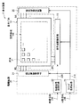
図1は、本技術による一実施の形態に係る表示装置1の概略構成を表したものである。この表示装置1は、表示パネル10と、表示パネル10を駆動する駆動回路20とを備えている。駆動回路20は、例えば、タイミング生成回路21、映像信号処理回路22、信号線駆動回路23、走査線駆動回路24、および電源線駆動回路25を有している。
<1. Embodiment>
[Constitution]
FIG. 1 illustrates a schematic configuration of a
(表示パネル10)
表示パネル10は、複数の画素11が表示パネル10の表示領域10A全面に渡って2次元配置されたものである。画素11は、表示パネル110上の画面を構成する最小単位の点に対応するものである。表示パネル10がカラー表示パネルである場合には、画素11は、例えば赤、緑または青などの単色の光を発する副画素に相当し、表示パネル10がモノクロ表示パネルである場合には、画素11は、白色光を発する画素に相当する。
(Display panel 10)
The
表示パネル10は、駆動回路20によって各画素11がアクティブマトリクス駆動されることにより、外部から入力された映像信号20Aに基づく画像を表示するものである。図2は、画素11の回路構成の一例を表したものである。画素11は、例えば、図2に示したように、画素回路12と、有機EL素子13とを有している。
The
画素回路12は、例えば、図2に示したように、駆動トランジスタTr1、書き込みトランジスタTr2および保持容量Csによって構成されたものであり、2Tr1Cの回路構成となっている。書き込みトランジスタTr2は、後述の信号線DTLの電圧をサンプリングするとともに駆動トランジスタTr1のゲートに書き込むものである。駆動トランジスタTr1は、書き込みトランジスタTr2によって書き込まれた電圧の大きさに応じて有機EL素子13に流れる電流を制御するものである。保持容量Csは、駆動トランジスタTr1のゲート−ソース間に所定の電圧を保持するものである。なお、画素回路12は、上述の2Tr1Cの回路構成とは異なる回路構成となっていてもよい。
For example, as illustrated in FIG. 2, the pixel circuit 12 includes a drive transistor Tr1, a write transistor Tr2, and a storage capacitor Cs, and has a circuit configuration of 2Tr1C. The write transistor Tr2 samples a voltage of a signal line DTL, which will be described later, and writes it to the gate of the drive transistor Tr1. The drive transistor Tr1 controls the current flowing through the
駆動トランジスタTr1および書き込みトランジスタTr2は、例えば、nチャネルMOS型の薄膜トランジスタ(TFT(Thin Film Transistor))により形成されている。なお、TFTの種類は特に限定されるものではなく、例えば、逆スタガー構造(ボトムゲート型)であってもよいし、スタガー構造(トップゲート型)であってもよい。また、駆動トランジスタTr1または書き込みトランジスタTr2は、pチャネルMOS型のTFTであってもよい。 The drive transistor Tr1 and the write transistor Tr2 are formed of, for example, an n-channel MOS thin film transistor (TFT (Thin Film Transistor)). Note that the type of TFT is not particularly limited, and may be, for example, an inverted stagger structure (bottom gate type) or a stagger structure (top gate type). Further, the drive transistor Tr1 or the write transistor Tr2 may be a p-channel MOS type TFT.
表示パネル10は、図2に示したように、行方向に延在する複数の書込線WSLと、列方向に延在する複数の信号線DTLと、行方向に延在する複数の電源線DSLとを有している。各信号線DTLと各書込線WSLとの交差点近傍には、画素11が設けられている。各信号線DTLは、後述の信号線駆動回路23の出力端(図示せず)と、書き込みトランジスタTr2のソースまたはドレインとに接続されている。各書込線WSLは、後述の書込線駆動回路24の出力端(図示せず)と、書き込みトランジスタTr2のゲートに接続されている。各電源線DSLは、固定の電圧を出力する電源の出力端(図示せず)と、駆動トランジスタTr1のソースまたはドレインに接続されている。
As shown in FIG. 2, the
書き込みトランジスタTr2のゲートは、書込線WSLに接続されている。書き込みトランジスタTr2のソースまたはドレインが信号線DTLに接続され、書き込みトランジスタTr2のソースおよびドレインのうち信号線DTLに未接続の端子が駆動トランジスタTr1のゲートに接続されている。駆動トランジスタTr1のソースまたはドレインが電源線DSLに接続され、駆動トランジスタTr1のソースおよびドレインのうち電源線DSLに未接続の端子が有機EL素子13のアノードに接続されている。保持容量Csの一端が駆動トランジスタTr1のゲートに接続され、保持容量Csの他端が駆動トランジスタTr1のソース(図2では有機EL素子13側の端子)に接続されている。つまり、保持容量Csは、駆動トランジスタTr1のゲート−ソース間に挿入されている。有機EL素子13のカソードは、グラウンド線GNDに接続されている。グラウンド線GNDは、基準電位(例えばグラウンド電位)となっている外部回路(図示せず)と電気的に接続されるものである。
The gate of the write transistor Tr2 is connected to the write line WSL. The source or drain of the write transistor Tr2 is connected to the signal line DTL, and the terminal not connected to the signal line DTL among the source and drain of the write transistor Tr2 is connected to the gate of the drive transistor Tr1. The source or drain of the drive transistor Tr1 is connected to the power supply line DSL, and the terminal not connected to the power supply line DSL among the source and drain of the drive transistor Tr1 is connected to the anode of the
(表示パネル10内の構造)
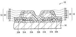
次に、図3、図4を参照しつつ、表示パネル10内の構造について説明する。図3は、表示パネル10内の有機EL素子13およびその近傍の断面構成の一例を表したものである。図4は、表示パネル10内の有機EL素子13およびその近傍の断面構成の他の例を表したものである。表示パネル10は、例えば、図3、図4に示したように、TFT基板14上に、各画素11に対応して設けられた複数の有機EL素子13を有している。なお、TFT基板14は、画素回路12などの形成された基板であって、かつ、少なくとも最上面に、画素回路12と電気的に接続された金属層(図示せず)を有している。有機EL素子13は、その金属層に接して形成されている。
(Structure in the display panel 10)
Next, the structure inside the
有機EL素子13は、例えば、図3、図4に示したように、TFT基板14側に設けられたアノード電極31と、アノード電極31上に設けられた有機層32と、有機層32上に設けられたカソード電極33とを有している。アノード電極31は、有機層32へ正孔を注入するものである。アノード電極31は、例えば、正孔注入性の良い材料で構成されており、例えばAl系金属で構成されている。Al系金属は、AlやAl合金を含む概念である。有機層32は、有機層32内に流れる電流量に応じた明るさで発光するものである。有機層32は、例えば、アノード電極31側から順に、正孔注入効率を高める正孔注入層32Aと、後述の発光層32Cへの正孔輸送効率を高める正孔輸送層32Bと、電子と正孔との再結合により発光する発光層32Cと、発光層32Cへの電子輸送効率を高める電子輸送層32Dとを積層してなる積層構造を有している。カソード電極33は、有機層32へ電子を注入するためのものである。カソード電極33は、電子注入性の良い材料で構成されており、例えば、MgAgなどの半透過型の金属材料で構成されている。有機EL素子13は低分子蒸着型の素子であり、有機層32は蒸着により形成されたものである。
For example, as shown in FIGS. 3 and 4, the
ところで、アノード電極31の側面は、当該アノード電極31のカソード電極33側の断面積が当該アノード電極31のカソード電極33とは反対側の断面積よりも大きくなるような構造となっている。アノード電極31の側面は、例えば、図3に示したように、逆テーパーになっている。なお、アノード電極31の側面は、例えば、図4に示したように、ひさし状になっていてもよい。
By the way, the side surface of the
有機層32のうち、発光層32C以外の全ての層は、表示領域10A内の全ての画素11を含む領域全体に渡って形成されている。一方、発光層32Cは、有機EL素子13ごとに選択的に形成されており、例えば、アノード電極31と対向する領域ごとに選択的に形成されている。ここで、正孔輸送層32Bおよび電子輸送層32Dは、全ての画素11で共通化されている。ただし、正孔輸送層32Bおよび電子輸送層32Dでは、抵抗率が正孔注入層32Aの抵抗率よりも大きく、しかも厚さが薄いため、積層面内方向の抵抗が大きくなっている。そのため、正孔輸送層32Bおよび電子輸送層32Dは、全ての画素11で共通化されているといっても、電気的には実質的に画素11ごとに分離されている。
Of the
一方、正孔注入層32Aは、各アノード電極31の側面に対応する箇所に高抵抗構造を有している。図3に記載の正孔注入層32Aでは、高抵抗構造は、段切れ構造である。この段切れ構造は、アノード電極31上に、正孔注入層32Aを蒸着により形成する際に、アノード電極31の側面に形成された逆テーパよって形成されたものである。図4に記載の正孔注入層32Aでも、高抵抗構造は、段切れ構造である。この段切れ構造は、アノード電極31上に、正孔注入層32Aを蒸着により形成する際に、アノード電極31の側面に形成されたひさし状の形状よって形成されたものである。
On the other hand, the
なお、図示しないが、上記の逆テーパや、ひさし状の形状における高さや奥行きの深さによっては、各アノード電極31の側面に対応する箇所に段切れ構造ができず、局所的な薄膜構造が形成されることもある。局所的な薄膜構造では、正孔注入層32Aの厚さが、正孔注入層32Aのうち、アノード電極31の側面に対応しない部位の厚さよりも薄くなっている。そのため、局所的な薄膜構造では、正孔注入層32Aの抵抗率が、正孔注入層32Aのうち、アノード電極31の側面に対応しない部位の抵抗率よりも高くなっている。従って、この場合には、高抵抗構造は、局所的な薄膜構造である。
Although not shown, depending on the reverse taper and the height and depth of the eaves-like shape, a stepped structure cannot be formed at a position corresponding to the side surface of each
図5、図6は、画素間に流れるリーク電流を電流密度の分布で表したものであり、具体的には図中の左側の画素を発光させたときの、その画素の周囲の電流密度の分布を表したものである。図5は、正孔注入層32Aに高抵抗構造が設けられているときの電流密度分布の一例を表したものである。図6は、正孔注入層32Aに高抵抗構造が設けられていないときの電流密度分布の一例を表したものである。図5、図6において、縦軸の電流密度は、図中の左側の画素を発光させた時に、その画素に流れる電流の密度で規格化されている。
5 and 6 show the leakage current flowing between the pixels as a current density distribution. Specifically, the current density around the pixel when the pixel on the left side in the figure is caused to emit light is shown. It represents the distribution. FIG. 5 shows an example of a current density distribution when a high resistance structure is provided in the
図5では、正孔注入層32Aの高抵抗構造の位置で、電流密度が不連続に変化しており、しかも急激に減少している。そのため、発光画素に隣接する画素(図5の右側の画素)には、発光画素からのリーク電流が到達していない。一方、図6では、電流密度が発光画素から遠ざかるにつれて、なだらかに減少している。そのため、発光画素からのリーク電流が、発光画素に隣接する画素(図5の右側の画素)にまで到達している。以上のことから、正孔注入層32Aの高抵抗構造が、発光画素からのリーク電流を効果的に遮断していることがわかる。
In FIG. 5, the current density changes discontinuously at the position of the high resistance structure of the
(駆動回路20)
次に、駆動回路20について簡単に説明する。駆動回路20は、上述したように、例えば、図1に示したように、タイミング生成回路21、映像信号処理回路22、信号線駆動回路23、書込線駆動回路24および電源線駆動回路25を有している。タイミング生成回路21は、駆動回路20内の各回路が連動して動作するように制御するものである。タイミング生成回路21は、例えば、外部から入力された同期信号20Bに応じて(同期して)、上述した各回路に対して制御信号21Aを出力するようになっている。
(Drive circuit 20)
Next, the
映像信号処理回路22は、外部から入力されたデジタルの映像信号20Aを補正すると共に、補正した後の映像信号をアナログに変換して信号線駆動回路23に出力するものである。信号線駆動回路23は、映像信号処理回路22から入力されたアナログの映像信号を、制御信号21Aの入力に応じて(同期して)各信号線DTLに出力するものである。書込線駆動回路24は、制御信号21Aの入力に応じて(同期して)、複数の書込線WSLを所定の単位ごとに順次選択するものである。電源線駆動回路25は、例えば、制御信号21Aの入力に応じて(同期して)、複数の電源線DSLを所定の単位ごとに順次選択するものである。なお、コンタクト構造14を介して接続端子15から出力される電流量は、電源線駆動回路25による電源線DSLの選択の態様に応じて変化する。
The video
[有機EL素子13の製造方法]
次に、図7を参照しつつ、有機EL素子13の製造方法について説明する。図7は、有機EL素子13の製造過程の一例を表したものである。
[Method for Manufacturing Organic EL Element 13]
Next, a method for manufacturing the
まず、TFT基板14上にアノード電極31を形成する(図7(A))。例えば、TFT基板14上に、すり鉢状の開口を有するマスク層を形成し、その開口に、所定の金属材料を充填する。その後、マスク層を除去する。これにより、側面が逆テーパとなったアノード電極31を形成することができる。
First, the
なお、正孔注入層32Aの側面をひさし状にする場合には、例えば、以下のようにする。まず、TFT基板14上に、開口を有する第1マスク層を形成し、その開口に、所定の金属材料を充填する。次に、先の開口よりも大きな径の開口を有する第2マスク層を形成する。このとき、充填した金属材料の上面全体が開口の底面に露出するように第2マスク層を形成する。その後、第2マスク層の開口に、所定の金属材料を充填する。その後、第1マスク層および第2マスク層を除去する。これにより、側面がひさし状となったアノード電極31を形成することができる。
In addition, when making the side surface of the
次に、例えば蒸着法を用いて、アノード電極31を含む所定の領域(表示領域10A内の全ての画素11を含む領域に対応する領域)全体に渡って、正孔注入層32Aを構成する材料を積層する。これにより、図7(B)に示したように、アノード電極31の側面に対応して高抵抗構造(段切れ構造)が形成された正孔注入層32Aを形成することができる。その後は、例えば蒸着法を用いて、正孔輸送層32B、有機層32Cおよび電子輸送層32Dを順次形成する。例えば、正孔注入層32Aの上面上に正孔輸送層32Bを形成し、正孔輸送層32Bの上面のうちアノード電極31の直上に有機層32Cを形成し、有機層32Cを含む所定の領域全体に渡って、電子輸送層32Dを形成する。このようにして、TFT基板14上に有機層13を形成する。その後、有機層13を含む表面全体にカソード電極33を形成する。このようにして、TFT基板14上に有機EL素子13を形成することができる。
Next, the material constituting the
[効果]
次に、本実施の形態の表示装置1の効果について説明する。
[effect]
Next, effects of the
有機EL素子が低分子蒸着型である場合に、有機EL素子をアレイ状に並べるときには、発光層は、通常、蒸着マスクを用いて画素毎に選択的に蒸着することにより形成される。しかし、有機層のうち発光層以外の層は、生産性の向上や、生産コストの削減を考えると、各画素で共通に形成されることが望ましい。とはいえ、正孔注入層を各画素で共通化すると、正孔注入層の抵抗率の低さにより、隣接する画素間でリーク電流が生じる。例えば、図6に示したように、発光画素からのリーク電流が、発光画素に隣接する画素(図6の右側の画素)に到達する。そのため、所望の画素以外の画素までもが発光するので、混色が発生し、画質が低下してしまう。 When the organic EL elements are of a low molecular vapor deposition type, when the organic EL elements are arranged in an array, the light emitting layer is usually formed by selectively depositing each pixel using a deposition mask. However, it is desirable that the layers other than the light emitting layer in the organic layer are formed in common for each pixel in consideration of improvement in productivity and reduction in production cost. However, if the hole injection layer is shared by each pixel, a leak current is generated between adjacent pixels due to the low resistivity of the hole injection layer. For example, as shown in FIG. 6, the leakage current from the light emitting pixel reaches a pixel adjacent to the light emitting pixel (the pixel on the right side in FIG. 6). For this reason, even pixels other than the desired pixel emit light, so that color mixing occurs and image quality deteriorates.
一方、本実施の形態では、アノード電極31の側面31Aが、当該アノード電極31のカソード電極33側の断面積が当該アノード電極31のカソード電極33とは反対側の断面積よりも大きくなるような構造となっている。具体的には、アノード電極31の側面31Aが、逆テーパー、またはひさし状となっている。これにより、例えば、正孔注入層32Aを、表示領域10A内の全ての画素11を含む領域に対応する領域全体に渡って積層したときに、正孔注入層32Aのうち各アノード電極31の側面31Aに対応する箇所に高抵抗構造が形成される。その結果、例えば、図5に示したように、正孔注入層32Aの高抵抗構造の位置で、電流密度が急激に減少するので、隣接する画素11間にリーク電流が生じるのを抑制することができる。その結果、混色や画質低下を抑制することが可能となる。
On the other hand, in the present embodiment, the
<2.適用例>
以下、上記各実施の形態およびそれらの変形例で説明した表示装置1の適用例について説明する。上述の表示装置1は、テレビジョン装置、デジタルカメラ、ノート型パーソナルコンピュータ、携帯電話等の携帯端末装置あるいはビデオカメラなど、外部から入力された映像信号あるいは内部で生成した映像信号を、映像あるいは映像として表示するあらゆる分野の電子機器の表示装置に適用することが可能である。
<2. Application example>
Hereinafter, application examples of the
(モジュール)
上述の表示装置1は、例えば、図8に示したようなモジュールとして、後述する適用例1〜5などの種々の電子機器に組み込まれる。このモジュールは、例えば、基板34の一辺に、封止用基板35から露出した領域210を設け、この露出した領域210に、駆動回路20の配線を延長して外部接続端子(図示せず)を形成したものである。外部接続端子には、信号の入出力のためのフレキシブルプリント配線基板(FPC;Flexible Printed Circuit)220が設けられていてもよい。
(module)
The above-described
(適用例1)
図9は、上述の表示装置1が適用されるテレビジョン装置の外観を表したものである。このテレビジョン装置は、例えば、フロントパネル310およびフィルターガラス320を含む映像表示画面部300を有しており、この映像表示画面部300は、上述の表示装置1により構成されている。
(Application example 1)
FIG. 9 illustrates an appearance of a television device to which the above-described
(適用例2)
図10は、上述の表示装置1が適用されるデジタルカメラの外観を表したものである。このデジタルカメラは、例えば、フラッシュ用の発光部410、表示部420、メニュースイッチ430およびシャッターボタン440を有しており、その表示部420は、上述の表示装置1により構成されている。
(Application example 2)
FIG. 10 shows the appearance of a digital camera to which the above-described
(適用例3)
図11は、上述の表示装置1が適用されるノート型パーソナルコンピュータの外観を表したものである。このノート型パーソナルコンピュータは、例えば、本体510,文字等の入力操作のためのキーボード520および映像を表示する表示部530を有しており、その表示部530は、上述の表示装置1により構成されている。
(Application example 3)
FIG. 11 shows the appearance of a notebook personal computer to which the above-described
(適用例4)
図12は、上述の表示装置1が適用されるビデオカメラの外観を表したものである。このビデオカメラは、例えば、本体部610,この本体部610の前方側面に設けられた被写体撮影用のレンズ620,撮影時のスタート/ストップスイッチ630および表示部640を有しており、その表示部640は、上述の表示装置1により構成されている。
(Application example 4)
FIG. 12 shows the appearance of a video camera to which the
(適用例5)
図13は、上述の表示装置1が適用される携帯電話機の外観を表したものである。この携帯電話機は、例えば、上側筐体710と下側筐体720とを連結部(ヒンジ部)730で連結したものであり、ディスプレイ740,サブディスプレイ750,ピクチャーライト760およびカメラ770を有している。そのディスプレイ740またはサブディスプレイ750は、上述の表示装置1により構成されている。
(Application example 5)
FIG. 13 shows the appearance of a mobile phone to which the above-described
以上、実施の形態、変形例および適用例を挙げて本技術を説明したが、本技術は上記実施の形態等に限定されるものではなく、種々変形が可能である。 Although the present technology has been described with the embodiment, the modification, and the application example, the present technology is not limited to the above-described embodiment and the like, and various modifications can be made.
例えば、上記実施の形態等では、上述の表示装置1がアクティブマトリクス型である場合について説明したが、アクティブマトリクス駆動のための画素回路12の構成は上記実施の形態等で説明したものに限られず、必要に応じて容量素子やトランジスタを画素回路12に追加してもよい。その場合、画素回路12の変更に応じて、上述した信号線駆動回路23、書込線駆動回路24、電源線駆動回路25のほかに、必要な駆動回路を追加してもよい。
For example, in the above-described embodiment, the case where the above-described
また、例えば、上記実施の形態等では、映像信号処理回路22、信号線駆動回路23、書込線駆動回路24、電源線駆動回路25の駆動をタイミング生成回路21が制御していたが、他の回路がこれらの駆動を制御するようにしてもよい。また、映像信号処理回路22、信号線駆動回路23、書込線駆動回路24、電源線駆動回路25の制御は、ハードウェア(回路)で行われていてもよいし、ソフトウェア(プログラム)で行われていてもよい。
Further, for example, in the above-described embodiment, the
また、例えば、本技術は以下のような構成を取ることができる。
(1)
表示領域に複数の画素を備え、
各画素は、有機EL素子と、前記有機EL素子を駆動する画素回路とを有し、
前記有機EL素子は、アノード電極と、カソード電極と、前記アノード電極と前記カソード電極との間に設けられた有機層とを有し、
前記アノード電極の側面は、当該アノード電極の前記カソード電極側の断面積が当該アノード電極の前記カソード電極とは反対側の断面積よりも大きくなるような構造となっている
表示パネル。
(2)
前記有機層は、正孔注入効率を高める正孔注入層と、正孔輸送効率を高める正孔輸送層と、電子と正孔との再結合により発光する発光層と、電子輸送効率を高める電子輸送層とを有し、
前記有機層のうち少なくとも正孔注入層は、前記表示領域内の全ての画素を含む領域全体に渡って形成されており、かつ、各アノード電極の側面に対応する箇所に高抵抗構造を有する
(1)に記載の表示パネル。
(3)
前記高抵抗構造は、段切れ構造、または局所的な薄膜構造である
(2)に記載の表示パネル。
(4)
前記アノード電極の側面は、逆テーパーになっている
(1)ないし(3)のいずれか1つに記載の表示パネル。
(5)
前記アノード電極の側面は、ひさし状になっている
(1)ないし(3)のいずれか1つに記載の表示パネル。
(6)
前記有機層は、蒸着によって形成されたものである
(1)ないし(5)のいずれか1つに記載の表示パネル。
(7)
表示領域に複数の画素を備えた表示パネルと、各画素を駆動する駆動回路とを備え、
各画素は、有機EL素子と、前記有機EL素子を駆動する画素回路とを有し、
前記有機EL素子は、アノード電極と、カソード電極と、前記アノード電極と前記カソード電極との間に設けられた有機層とを有し、
前記アノード電極の側面は、当該アノード電極の前記カソード電極側の断面積が当該アノード電極の前記カソード電極とは反対側の断面積よりも大きくなるような構造となっている
表示装置。
(8)
表示装置を備え、
前記表示装置は、表示領域に複数の画素を備えた表示パネルと、各画素を駆動する駆動回路とを有し、
各画素は、有機EL素子と、前記有機EL素子を駆動する画素回路とを有し、
前記有機EL素子は、アノード電極と、カソード電極と、前記アノード電極と前記カソード電極との間に設けられた有機層とを有し、
前記アノード電極の側面は、当該アノード電極の前記カソード電極側の断面積が当該アノード電極の前記カソード電極とは反対側の断面積よりも大きくなるような構造となっている
電子機器。
For example, this technique can take the following composition.
(1)
The display area has a plurality of pixels,
Each pixel has an organic EL element and a pixel circuit that drives the organic EL element,
The organic EL element has an anode electrode, a cathode electrode, and an organic layer provided between the anode electrode and the cathode electrode,
The side surface of the anode electrode has a structure in which a cross-sectional area of the anode electrode on the cathode electrode side is larger than a cross-sectional area of the anode electrode on the side opposite to the cathode electrode.
(2)
The organic layer includes a hole injection layer that increases hole injection efficiency, a hole transport layer that increases hole transport efficiency, a light emitting layer that emits light by recombination of electrons and holes, and an electron that increases electron transport efficiency. A transport layer,
Among the organic layers, at least the hole injection layer is formed over the entire region including all the pixels in the display region, and has a high resistance structure at a position corresponding to the side surface of each anode electrode. The display panel according to 1).
(3)
The display panel according to (2), wherein the high resistance structure is a stepped structure or a local thin film structure.
(4)
The display panel according to any one of (1) to (3), wherein a side surface of the anode electrode has an inverse taper.
(5)
The display panel according to any one of (1) to (3), wherein a side surface of the anode electrode has an eaves shape.
(6)
The display panel according to any one of (1) to (5), wherein the organic layer is formed by vapor deposition.
(7)
A display panel having a plurality of pixels in a display area, and a drive circuit for driving each pixel;
Each pixel has an organic EL element and a pixel circuit that drives the organic EL element,
The organic EL element has an anode electrode, a cathode electrode, and an organic layer provided between the anode electrode and the cathode electrode,
The side surface of the anode electrode has a structure in which a cross-sectional area of the anode electrode on the cathode electrode side is larger than a cross-sectional area of the anode electrode on the side opposite to the cathode electrode.
(8)
A display device,
The display device includes a display panel including a plurality of pixels in a display area, and a drive circuit that drives each pixel.
Each pixel has an organic EL element and a pixel circuit that drives the organic EL element,
The organic EL element has an anode electrode, a cathode electrode, and an organic layer provided between the anode electrode and the cathode electrode,
The electronic device has a structure in which a side surface of the anode electrode has a cross-sectional area of the anode electrode on the cathode electrode side larger than a cross-sectional area of the anode electrode on the side opposite to the cathode electrode.
1…表示装置、10…表示パネル、10A…表示領域、11…画素、12…画素回路、13…有機EL素子、14…TFT基板、20…駆動回路、20A…映像信号、20B…同期信号、21…タイミング生成回路、21A…制御信号、22…映像信号処理回路、23…信号線駆動回路、24…書込線駆動回路、25…電源線駆動回路、31…アノード電極、31A…側面、32…有機層、32A…正孔注入層、32B…正孔輸送層、32C…発光層、32D…電子輸送層、33…カソード電極、34…基板、35…封止用基板、210…領域、220…FPC、300…映像表示画面部、310…フロントパネル、320…フィルターガラス、410…発光部、420,530,640…表示部、430…メニュースイッチ、440…シャッターボタン、510…本体、520…キーボード、610…本体部、620…レンズ、630…スタート/ストップスイッチ、710…上側筐体、720…下側筐体、730…連結部、740…ディスプレイ、750…サブディスプレイ、760…ピクチャーライト、770…カメラ、Cs…保持容量、DTL…信号線、GND…グラウンド線、DSL…電源線、Tr1…駆動トランジスタ、Tr2…書き込みトランジスタ、WSL…書込線。
DESCRIPTION OF
Claims (5)
各画素は、有機EL素子と、前記有機EL素子を駆動する画素回路とを有し、
前記有機EL素子は、Al系金属で構成されたアノード電極と、カソード電極と、前記アノード電極と前記カソード電極との間に設けられた有機層とを有し、
前記アノード電極の側面は、当該アノード電極の前記カソード電極側の断面積が当該アノード電極の前記カソード電極とは反対側の断面積よりも大きくなるような構造となっており、
前記有機層は、正孔注入効率を高める正孔注入層と、正孔輸送効率を高める正孔輸送層と、電子と正孔との再結合により発光する発光層と、電子輸送効率を高める電子輸送層とを有し、
前記有機層のうち少なくとも正孔注入層は、前記表示領域内の全ての画素を含む領域全体に渡って形成されており、かつ、各アノード電極の側面に対応する箇所に高抵抗構造を有し、
前記高抵抗構造は、段切れ構造、または局所的な薄膜構造である
表示パネル。 The display area has a plurality of pixels,
Each pixel has an organic EL element and a pixel circuit that drives the organic EL element,
The organic EL element has an anode electrode made of an Al-based metal, a cathode electrode, and an organic layer provided between the anode electrode and the cathode electrode,
The side surface of the anode electrode has a structure in which a cross-sectional area of the anode electrode on the cathode electrode side is larger than a cross-sectional area of the anode electrode on the side opposite to the cathode electrode ,
The organic layer includes a hole injection layer that increases hole injection efficiency, a hole transport layer that increases hole transport efficiency, a light emitting layer that emits light by recombination of electrons and holes, and an electron that increases electron transport efficiency. A transport layer,
At least the hole injection layer in the organic layer is formed over the entire region including all the pixels in the display region, and has a high resistance structure at a position corresponding to the side surface of each anode electrode. ,
The high resistance structure is a display panel having a stepped structure or a local thin film structure .
請求項1に記載の表示パネル。 The display panel according to claim 1 , wherein a side surface of the anode electrode has an inverse taper.
請求項1に記載の表示パネル。 The display panel according to claim 1 , wherein a side surface of the anode electrode has a peak shape.
各画素は、有機EL素子と、前記有機EL素子を駆動する画素回路とを有し、
前記有機EL素子は、Al系金属で構成されたアノード電極と、カソード電極と、前記アノード電極と前記カソード電極との間に設けられた有機層とを有し、
前記アノード電極の側面は、当該アノード電極の前記カソード電極側の断面積が当該アノード電極の前記カソード電極とは反対側の断面積よりも大きくなるような構造となっており、
前記有機層は、正孔注入効率を高める正孔注入層と、正孔輸送効率を高める正孔輸送層と、電子と正孔との再結合により発光する発光層と、電子輸送効率を高める電子輸送層とを有し、
前記有機層のうち少なくとも正孔注入層は、前記表示領域内の全ての画素を含む領域全体に渡って形成されており、かつ、各アノード電極の側面に対応する箇所に高抵抗構造を有し、
前記高抵抗構造は、段切れ構造、または局所的な薄膜構造である
表示装置。 A display panel having a plurality of pixels in a display area, and a drive circuit for driving each pixel;
Each pixel has an organic EL element and a pixel circuit that drives the organic EL element,
The organic EL element has an anode electrode made of an Al-based metal, a cathode electrode, and an organic layer provided between the anode electrode and the cathode electrode,
The side surface of the anode electrode has a structure in which a cross-sectional area of the anode electrode on the cathode electrode side is larger than a cross-sectional area of the anode electrode on the side opposite to the cathode electrode ,
The organic layer includes a hole injection layer that increases hole injection efficiency, a hole transport layer that increases hole transport efficiency, a light emitting layer that emits light by recombination of electrons and holes, and an electron that increases electron transport efficiency. A transport layer,
At least the hole injection layer in the organic layer is formed over the entire region including all the pixels in the display region, and has a high resistance structure at a position corresponding to the side surface of each anode electrode. ,
The display device in which the high resistance structure is a stepped structure or a local thin film structure .
前記表示装置は、表示領域に複数の画素を備えた表示パネルと、各画素を駆動する駆動回路とを有し、
各画素は、有機EL素子と、前記有機EL素子を駆動する画素回路とを有し、
前記有機EL素子は、Al系金属で構成されたアノード電極と、カソード電極と、前記アノード電極と前記カソード電極との間に設けられた有機層とを有し、
前記アノード電極の側面は、当該アノード電極の前記カソード電極側の断面積が当該アノード電極の前記カソード電極とは反対側の断面積よりも大きくなるような構造となっており、
前記有機層は、正孔注入効率を高める正孔注入層と、正孔輸送効率を高める正孔輸送層と、電子と正孔との再結合により発光する発光層と、電子輸送効率を高める電子輸送層とを有し、
前記有機層のうち少なくとも正孔注入層は、前記表示領域内の全ての画素を含む領域全体に渡って形成されており、かつ、各アノード電極の側面に対応する箇所に高抵抗構造を有し、
前記高抵抗構造は、段切れ構造、または局所的な薄膜構造である
電子機器。 A display device,
The display device includes a display panel including a plurality of pixels in a display area, and a drive circuit that drives each pixel.
Each pixel has an organic EL element and a pixel circuit that drives the organic EL element,
The organic EL element has an anode electrode made of an Al-based metal, a cathode electrode, and an organic layer provided between the anode electrode and the cathode electrode,
The side surface of the anode electrode has a structure in which a cross-sectional area of the anode electrode on the cathode electrode side is larger than a cross-sectional area of the anode electrode on the side opposite to the cathode electrode ,
The organic layer includes a hole injection layer that increases hole injection efficiency, a hole transport layer that increases hole transport efficiency, a light emitting layer that emits light by recombination of electrons and holes, and an electron that increases electron transport efficiency. A transport layer,
At least the hole injection layer in the organic layer is formed over the entire region including all the pixels in the display region, and has a high resistance structure at a position corresponding to the side surface of each anode electrode. ,
The high resistance structure is an electronic device having a stepped structure or a local thin film structure .
Priority Applications (4)
| Application Number | Priority Date | Filing Date | Title |
|---|---|---|---|
| JP2011229995A JP5919723B2 (en) | 2011-10-19 | 2011-10-19 | Display panel, display device and electronic device |
| PCT/JP2012/076179 WO2013058146A1 (en) | 2011-10-19 | 2012-10-10 | Display panel, display device, and electronic apparatus |
| US14/346,889 US9401494B2 (en) | 2011-10-19 | 2012-10-10 | Display panel, display unit, and electronic apparatus |
| CN201280050067.5A CN103891408B (en) | 2011-10-19 | 2012-10-10 | Display floater, display unit and electronic equipment |
Applications Claiming Priority (1)
| Application Number | Priority Date | Filing Date | Title |
|---|---|---|---|
| JP2011229995A JP5919723B2 (en) | 2011-10-19 | 2011-10-19 | Display panel, display device and electronic device |
Publications (3)
| Publication Number | Publication Date |
|---|---|
| JP2013089505A JP2013089505A (en) | 2013-05-13 |
| JP2013089505A5 JP2013089505A5 (en) | 2014-11-06 |
| JP5919723B2 true JP5919723B2 (en) | 2016-05-18 |
Family
ID=48140794
Family Applications (1)
| Application Number | Title | Priority Date | Filing Date |
|---|---|---|---|
| JP2011229995A Active JP5919723B2 (en) | 2011-10-19 | 2011-10-19 | Display panel, display device and electronic device |
Country Status (4)
| Country | Link |
|---|---|
| US (1) | US9401494B2 (en) |
| JP (1) | JP5919723B2 (en) |
| CN (1) | CN103891408B (en) |
| WO (1) | WO2013058146A1 (en) |
Families Citing this family (7)
| Publication number | Priority date | Publication date | Assignee | Title |
|---|---|---|---|---|
| EP3002797B1 (en) * | 2014-09-30 | 2020-04-29 | Novaled GmbH | A light emitting organic device and an active OLED display |
| JP7203499B2 (en) * | 2018-03-07 | 2023-01-13 | 株式会社ジャパンディスプレイ | Display device |
| TWI675472B (en) * | 2018-08-14 | 2019-10-21 | 友達光電股份有限公司 | Organic light emitting device and fabricating method thereof |
| CN110299389B (en) * | 2019-06-26 | 2021-06-04 | 合肥视涯技术有限公司 | Organic light emitting display device |
| CN113078270A (en) * | 2020-01-06 | 2021-07-06 | 京东方科技集团股份有限公司 | Organic electroluminescent structure, manufacturing method thereof and display device |
| CN114864838A (en) * | 2020-01-06 | 2022-08-05 | 京东方科技集团股份有限公司 | Organic electroluminescent structure and display device |
| JP2021163577A (en) * | 2020-03-31 | 2021-10-11 | ソニーセミコンダクタソリューションズ株式会社 | Display device and electronic apparatus |
Family Cites Families (12)
| Publication number | Priority date | Publication date | Assignee | Title |
|---|---|---|---|---|
| US20020036291A1 (en) * | 2000-06-20 | 2002-03-28 | Parker Ian D. | Multilayer structures as stable hole-injecting electrodes for use in high efficiency organic electronic devices |
| KR100712295B1 (en) * | 2005-06-22 | 2007-04-27 | 삼성에스디아이 주식회사 | Organic electroluminescence device and method for fabricating the same |
| JP4203772B2 (en) | 2006-08-01 | 2009-01-07 | ソニー株式会社 | Display device and driving method thereof |
| KR100823511B1 (en) * | 2006-11-10 | 2008-04-21 | 삼성에스디아이 주식회사 | Organic light emission display and fabrication method thereof |
| JP2008235066A (en) * | 2007-03-22 | 2008-10-02 | Toppan Printing Co Ltd | Organic el element and its manufacturing method |
| WO2009133680A1 (en) * | 2008-04-28 | 2009-11-05 | パナソニック株式会社 | Display device and method for manufacturing same |
| JP5199773B2 (en) * | 2008-07-30 | 2013-05-15 | 住友化学株式会社 | Organic electroluminescence device and method for producing the same |
| WO2010134237A1 (en) * | 2009-05-22 | 2010-11-25 | シャープ株式会社 | Organic el display device and method for manufacturing same |
| JP5633516B2 (en) * | 2009-09-30 | 2014-12-03 | 凸版印刷株式会社 | Organic electroluminescent device, organic electroluminescent display panel, and organic electroluminescent display panel manufacturing method |
| CN102165593B (en) * | 2009-12-22 | 2015-01-28 | 松下电器产业株式会社 | Display device and manufacturing method thereof |
| KR101182442B1 (en) * | 2010-01-27 | 2012-09-12 | 삼성디스플레이 주식회사 | OLED display apparatus and Method thereof |
| JP5919807B2 (en) * | 2011-03-30 | 2016-05-18 | ソニー株式会社 | ORGANIC LIGHT EMITTING ELEMENT, METHOD FOR MANUFACTURING ORGANIC LIGHT EMITTING ELEMENT, AND DISPLAY DEVICE |
-
2011
- 2011-10-19 JP JP2011229995A patent/JP5919723B2/en active Active
-
2012
- 2012-10-10 WO PCT/JP2012/076179 patent/WO2013058146A1/en active Application Filing
- 2012-10-10 US US14/346,889 patent/US9401494B2/en not_active Expired - Fee Related
- 2012-10-10 CN CN201280050067.5A patent/CN103891408B/en active Active
Also Published As
| Publication number | Publication date |
|---|---|
| JP2013089505A (en) | 2013-05-13 |
| US20140231789A1 (en) | 2014-08-21 |
| WO2013058146A1 (en) | 2013-04-25 |
| CN103891408B (en) | 2016-08-17 |
| US9401494B2 (en) | 2016-07-26 |
| CN103891408A (en) | 2014-06-25 |
Similar Documents
| Publication | Publication Date | Title |
|---|---|---|
| US20190347992A1 (en) | Display device, method of laying out light emitting elements, and electronic device | |
| JP5811709B2 (en) | Luminescent panel, display device and electronic device | |
| JP5919723B2 (en) | Display panel, display device and electronic device | |
| US8581275B2 (en) | Organic EL display and electronic apparatus | |
| US9219087B2 (en) | Display, display drive method, method of manufacturing display, and electronic apparatus | |
| US8854283B2 (en) | Display apparatus, pixel layout method for display apparatus, and electronic device | |
| JP2013058323A (en) | Light-emitting panel, display device, and electronic apparatus | |
| JP2009169071A (en) | Display device | |
| JP2010002476A (en) | Light emission display and electronic apparatus | |
| TWI423220B (en) | Display device, method of laying out wiring in display device, and electronic device | |
| JP5392545B2 (en) | Display device | |
| JP2010003880A (en) | Display and electronic apparatus | |
| JP2009169070A (en) | Color image display device, shadow mask and method of manufacturing color image display device using shadow mask | |
| JP2010002531A (en) | Display device and electronic equipment | |
| JP5617319B2 (en) | Display device and electronic device | |
| JP2013057726A (en) | Display panel, display device and, electronic device | |
| JP2013089510A (en) | Display panel, display device and electronic apparatus | |
| JP5590285B2 (en) | Display device | |
| JP2012185327A (en) | Writing circuit, display panel, display device, and electronic appliance | |
| JP5737568B2 (en) | Display panel, display device and electronic device | |
| JP5927601B2 (en) | Luminescent panel, display device and electronic device | |
| JP5766491B2 (en) | Luminescent panel, display device and electronic device | |
| JP5737570B2 (en) | Display device and electronic device | |
| JP2013057737A (en) | Display panel and display device | |
| JP2013073051A (en) | Circuit board, manufacturing method thereof, and electronic apparatus |
Legal Events
| Date | Code | Title | Description |
|---|---|---|---|
| A521 | Request for written amendment filed |
Free format text: JAPANESE INTERMEDIATE CODE: A523 Effective date: 20140917 |
|
| A621 | Written request for application examination |
Free format text: JAPANESE INTERMEDIATE CODE: A621 Effective date: 20140917 |
|
| A131 | Notification of reasons for refusal |
Free format text: JAPANESE INTERMEDIATE CODE: A131 Effective date: 20150901 |
|
| A521 | Request for written amendment filed |
Free format text: JAPANESE INTERMEDIATE CODE: A523 Effective date: 20151014 |
|
| TRDD | Decision of grant or rejection written | ||
| A01 | Written decision to grant a patent or to grant a registration (utility model) |
Free format text: JAPANESE INTERMEDIATE CODE: A01 Effective date: 20160315 |
|
| A61 | First payment of annual fees (during grant procedure) |
Free format text: JAPANESE INTERMEDIATE CODE: A61 Effective date: 20160328 |
|
| R151 | Written notification of patent or utility model registration |
Ref document number: 5919723 Country of ref document: JP Free format text: JAPANESE INTERMEDIATE CODE: R151 |
|
| R250 | Receipt of annual fees |
Free format text: JAPANESE INTERMEDIATE CODE: R250 |
|
| R250 | Receipt of annual fees |
Free format text: JAPANESE INTERMEDIATE CODE: R250 |