JP5919807B2 - ORGANIC LIGHT EMITTING ELEMENT, METHOD FOR MANUFACTURING ORGANIC LIGHT EMITTING ELEMENT, AND DISPLAY DEVICE - Google Patents
ORGANIC LIGHT EMITTING ELEMENT, METHOD FOR MANUFACTURING ORGANIC LIGHT EMITTING ELEMENT, AND DISPLAY DEVICE Download PDFInfo
- Publication number
- JP5919807B2 JP5919807B2 JP2011281214A JP2011281214A JP5919807B2 JP 5919807 B2 JP5919807 B2 JP 5919807B2 JP 2011281214 A JP2011281214 A JP 2011281214A JP 2011281214 A JP2011281214 A JP 2011281214A JP 5919807 B2 JP5919807 B2 JP 5919807B2
- Authority
- JP
- Japan
- Prior art keywords
- electrode
- light emitting
- insulating film
- organic
- layer
- Prior art date
- Legal status (The legal status is an assumption and is not a legal conclusion. Google has not performed a legal analysis and makes no representation as to the accuracy of the status listed.)
- Expired - Fee Related
Links
Images


Classifications
-
- H—ELECTRICITY
- H10—SEMICONDUCTOR DEVICES; ELECTRIC SOLID-STATE DEVICES NOT OTHERWISE PROVIDED FOR
- H10K—ORGANIC ELECTRIC SOLID-STATE DEVICES
- H10K59/00—Integrated devices, or assemblies of multiple devices, comprising at least one organic light-emitting element covered by group H10K50/00
- H10K59/10—OLED displays
- H10K59/12—Active-matrix OLED [AMOLED] displays
- H10K59/122—Pixel-defining structures or layers, e.g. banks
-
- H—ELECTRICITY
- H10—SEMICONDUCTOR DEVICES; ELECTRIC SOLID-STATE DEVICES NOT OTHERWISE PROVIDED FOR
- H10K—ORGANIC ELECTRIC SOLID-STATE DEVICES
- H10K50/00—Organic light-emitting devices
- H10K50/80—Constructional details
- H10K50/805—Electrodes
- H10K50/81—Anodes
- H10K50/818—Reflective anodes, e.g. ITO combined with thick metallic layers
-
- H—ELECTRICITY
- H10—SEMICONDUCTOR DEVICES; ELECTRIC SOLID-STATE DEVICES NOT OTHERWISE PROVIDED FOR
- H10K—ORGANIC ELECTRIC SOLID-STATE DEVICES
- H10K50/00—Organic light-emitting devices
- H10K50/80—Constructional details
- H10K50/84—Passivation; Containers; Encapsulations
- H10K50/844—Encapsulations
-
- H—ELECTRICITY
- H10—SEMICONDUCTOR DEVICES; ELECTRIC SOLID-STATE DEVICES NOT OTHERWISE PROVIDED FOR
- H10K—ORGANIC ELECTRIC SOLID-STATE DEVICES
- H10K59/00—Integrated devices, or assemblies of multiple devices, comprising at least one organic light-emitting element covered by group H10K50/00
- H10K59/10—OLED displays
- H10K59/12—Active-matrix OLED [AMOLED] displays
- H10K59/123—Connection of the pixel electrodes to the thin film transistors [TFT]
-
- H—ELECTRICITY
- H10—SEMICONDUCTOR DEVICES; ELECTRIC SOLID-STATE DEVICES NOT OTHERWISE PROVIDED FOR
- H10K—ORGANIC ELECTRIC SOLID-STATE DEVICES
- H10K59/00—Integrated devices, or assemblies of multiple devices, comprising at least one organic light-emitting element covered by group H10K50/00
- H10K59/10—OLED displays
- H10K59/12—Active-matrix OLED [AMOLED] displays
- H10K59/126—Shielding, e.g. light-blocking means over the TFTs
-
- H—ELECTRICITY
- H10—SEMICONDUCTOR DEVICES; ELECTRIC SOLID-STATE DEVICES NOT OTHERWISE PROVIDED FOR
- H10K—ORGANIC ELECTRIC SOLID-STATE DEVICES
- H10K2102/00—Constructional details relating to the organic devices covered by this subclass
- H10K2102/301—Details of OLEDs
- H10K2102/302—Details of OLEDs of OLED structures
- H10K2102/3023—Direction of light emission
- H10K2102/3026—Top emission
-
- H—ELECTRICITY
- H10—SEMICONDUCTOR DEVICES; ELECTRIC SOLID-STATE DEVICES NOT OTHERWISE PROVIDED FOR
- H10K—ORGANIC ELECTRIC SOLID-STATE DEVICES
- H10K50/00—Organic light-emitting devices
- H10K50/80—Constructional details
- H10K50/85—Arrangements for extracting light from the devices
- H10K50/852—Arrangements for extracting light from the devices comprising a resonant cavity structure, e.g. Bragg reflector pair
-
- H—ELECTRICITY
- H10—SEMICONDUCTOR DEVICES; ELECTRIC SOLID-STATE DEVICES NOT OTHERWISE PROVIDED FOR
- H10K—ORGANIC ELECTRIC SOLID-STATE DEVICES
- H10K59/00—Integrated devices, or assemblies of multiple devices, comprising at least one organic light-emitting element covered by group H10K50/00
- H10K59/30—Devices specially adapted for multicolour light emission
Description
本技術は、有機層下に素子分離膜としての絶縁膜を有する有機発光素子、有機発光素子の製造方法および表示装置に関する。 The present technology relates to an organic light emitting element having an insulating film as an element separation film under an organic layer, a method for manufacturing the organic light emitting element , and a display device.
近年、フラットパネルディスプレイの一つとして、有機発光素子を用いた有機発光ディスプレイが注目されている。有機発光ディスプレイは、バックライトが不要なため薄型化・軽量化が可能となる。また、自発光型であるため視野角が広く、消費電力が低いという特性を有し、更に、高精細度の高速ビデオ信号に対しても十分な応答性を有するものと考えられており、実用化に向けて開発が進められている。 In recent years, an organic light emitting display using an organic light emitting element has attracted attention as one of flat panel displays. Organic light-emitting displays can be made thinner and lighter because no backlight is required. In addition, since it is a self-luminous type, it has the characteristics of wide viewing angle and low power consumption, and is considered to have sufficient response to high-definition high-speed video signals. Development is progressing toward the realization.
有機発光素子の構成としては、例えば、基板の上に、TFT(Thin Film Transistor;薄膜トランジスタ)および平坦化層などを間にして、第1電極,発光層を含む有機層および第2電極が順に形成されたものが知られている(例えば、特許文献1)。第1電極の周縁には、第1電極と第2電極との間の絶縁性を確保するために絶縁膜(素子分離膜)が設けられる(例えば、特許文献2,3)。この絶縁膜は非常に膜厚の薄い有機層や第2電極の断線による素子特性の劣化を防止するため、なだらかなテーパ形状で設けられる。 As a configuration of the organic light emitting element, for example, a first electrode, an organic layer including a light emitting layer, and a second electrode are sequentially formed on a substrate with a TFT (Thin Film Transistor) and a planarizing layer interposed therebetween. Is known (for example, Patent Document 1). An insulating film (element isolation film) is provided on the periphery of the first electrode in order to ensure insulation between the first electrode and the second electrode (for example, Patent Documents 2 and 3). This insulating film is provided with a gentle taper shape in order to prevent deterioration of element characteristics due to a very thin organic layer or disconnection of the second electrode.
しかしながら、このようななだらかなテーパ形状の絶縁膜では、第1電極が絶縁膜に広く覆われ、開口率が低くなるという問題が生じていた。特に小型の高精細な表示装置に適用させる場合には、この問題が大きく影響する。 However, such a gently tapered insulating film has a problem that the first electrode is widely covered with the insulating film and the aperture ratio is lowered. In particular, when applied to a small high-definition display device, this problem greatly affects.
本技術はかかる問題点に鑑みてなされたもので、その目的は、有機層および第2電極の断線を防止できると共に高開口率の有機発光素子、有機発光素子の製造方法および表示装置を提供することにある。 The present technology has been made in view of such problems, and an object thereof is to provide a high aperture ratio organic light emitting device , a method for manufacturing the organic light emitting device , and a display device that can prevent disconnection of the organic layer and the second electrode. There is.
本技術による第1の有機発光素子は、第1電極および第2電極と、第1電極と第2電極との間の、発光層を含む有機層と、第1電極の周縁を表面から側面にかけて覆うと共に有機層に接する内壁面を有し、その内壁面に、稜線が第1電極の表面に平行な少なくとも一つの角部を有する絶縁膜とを備え、内壁面のうち第1電極側の第1面の第1電極の表面とのなす角度は、70°以上90°未満であり、内壁面のうち第2電極側の第2面の第1電極の表面とのなす角度は、20°以上45°以下であるものである。 The first organic light emitting device according to the present technology includes a first electrode and a second electrode, an organic layer including a light emitting layer between the first electrode and the second electrode, and a periphery of the first electrode from the surface to the side surface. An inner wall surface covering and in contact with the organic layer, the inner wall surface including an insulating film having at least one corner parallel to the surface of the first electrode on the inner wall surface; The angle formed with the surface of the first electrode of one surface is 70 ° or more and less than 90 °, and the angle formed with the surface of the first electrode on the second electrode side of the inner wall surface is 20 ° or more. It is 45 degrees or less .
本技術による第2の有機発光素子は、第1電極および第2電極と、第1電極と前記第2電極との間の、発光層を含む有機層と、第1電極の側面を覆うと共に、側面の上端から下端にかけて傾斜面を有する絶縁膜とを備えたものである。 The second organic light emitting device according to the present technology covers the first electrode and the second electrode, the organic layer including the light emitting layer between the first electrode and the second electrode, the side surface of the first electrode, And an insulating film having an inclined surface from the upper end to the lower end of the side surface.
本技術による第1の表示装置は上記第1の有機発光素子、本技術による第2の表示装置は上記第2の有機発光素子をそれぞれ備えたものである。
本技術による有機発光素子の製造方法は、第1電極を形成し、第1電極の周縁を表面から側面にかけて覆う絶縁膜を形成し、第1電極との間に、発光層を含む有機層を設けて第2電極を形成し、絶縁膜の形成では、有機層に接する内壁面を形成するとともに、内壁面に、稜線が第1電極の表面に平行な少なくとも一つの角部を形成し、角部を絶縁膜に対する逆スパッタリング処理により形成して、内壁面のうち第1電極側の第1面の第1電極の表面とのなす角度を、70°以上90°未満とし、内壁面のうち第2電極側の第2面の第1電極の表面とのなす角度を、20°以上45°以下とするものである。
A first display device according to the present technology includes the first organic light-emitting element, and a second display device according to the present technology includes the second organic light-emitting element.
In the method for manufacturing an organic light emitting device according to the present technology, a first electrode is formed, an insulating film is formed to cover the periphery of the first electrode from the surface to the side surface, and an organic layer including a light emitting layer is formed between the first electrode and the first electrode. In the formation of the insulating film, the inner wall surface in contact with the organic layer is formed, and at least one corner portion whose ridge line is parallel to the surface of the first electrode is formed on the inner wall surface. And forming an angle between the first electrode side of the first electrode side of the inner wall surface and the surface of the first electrode at 70 ° or more and less than 90 °, An angle between the second electrode-side second surface and the surface of the first electrode is set to 20 ° to 45 °.
本技術の第1の有機発光素子、有機発光素子の製造方法または表示装置では、有機層に接する絶縁膜(素子分離膜)の内壁面に、当該角部を境として第1電極の表面(水平面)に対する傾斜角度が異なる複数の面、即ち、第1電極側の相対的に急峻な面(第1面)と、相対的により傾斜角度のなだらかな第2電極側の1または2以上の面(第2面)が存在する。この第2面によって第2電極での断線が抑制される一方、第1面では開口の大きさが確保される。 In the first organic light-emitting element , the method for manufacturing the organic light- emitting element , or the display device according to the present technology, the surface of the first electrode (horizontal plane) is formed on the inner wall surface of the insulating film (element separation film) in contact with the organic layer with the corner portion as a boundary. ) Having a different inclination angle, that is, a relatively steep surface (first surface) on the first electrode side and one or more surfaces on the second electrode side having a relatively gentle inclination angle (first surface). The second side) exists. While this second surface suppresses disconnection at the second electrode, the size of the opening is ensured on the first surface.
本技術の第2の有機発光素子または表示装置では、絶縁膜が第1電極の側面を上端から下端にかけて傾斜して覆うようにしたので、第1電極の表面には絶縁膜が形成されずに第1電極の表面全体が露出され、かつ、この絶縁膜の傾斜面によって第2電極の断線が抑えられる。 In the second organic light emitting element or the display device of the present technology, the insulating film covers the side surface of the first electrode so as to be inclined from the upper end to the lower end, so that the insulating film is not formed on the surface of the first electrode. The entire surface of the first electrode is exposed, and disconnection of the second electrode is suppressed by the inclined surface of the insulating film.
本技術の第1の有機発光素子、有機発光素子の製造方法および表示装置では、素子分離膜としての絶縁膜の内壁面に少なくとも一つの角部を設け、また、本技術の第2の有機発光素子および表示装置では、素子分離膜としての絶縁膜に傾斜面を設けるようにしたので、有機層および第2電極の断線を防止による素子特性の劣化を防止し、かつ、開口率を向上させることができる。 In the first organic light-emitting element , the method for manufacturing the organic light- emitting element , and the display device of the present technology, at least one corner is provided on the inner wall surface of the insulating film as the element isolation film, In the element and the display device, since the insulating film as the element isolation film is provided with the inclined surface, the element characteristic is prevented from being deteriorated by preventing disconnection of the organic layer and the second electrode, and the aperture ratio is improved. Can do.
以下、本技術の実施の形態について、図面を参照して詳細に説明する。なお、説明は以下の順序で行う。
1.第1の実施の形態(絶縁膜が角部を有する例)
2.変形例(絶縁膜が複数の角部を有する例)
3.第2の実施の形態(絶縁膜が傾斜面を有する例)
3.適用例
Hereinafter, embodiments of the present technology will be described in detail with reference to the drawings. The description will be given in the following order.
1. First embodiment (an example in which the insulating film has corners)
2. Modification (example where the insulating film has a plurality of corners)
3. Second embodiment (an example in which the insulating film has an inclined surface)
3. Application examples
〔第1の実施の形態〕
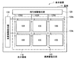
図1は、本開示の一実施の形態に係る表示装置(表示装置1)の構成を表すものである。この表示装置1は、有機EL(Electroluminescence)表示装置であり、基板11の上に、表示領域110として、複数の有機EL素子(有機発光素子)10R,10G,10Bがマトリクス状に配置されている。有機EL素子10R,10G,10Bは、それぞれ赤色の光(波長620nm〜750nm),緑色の光(波長495nm〜570nm),青色の光(波長450nm〜495nm)を発生する。表示領域110の周辺には、映像表示用の信号線駆動回路120および走査線駆動回路130が設けられている。
[First Embodiment]
FIG. 1 illustrates a configuration of a display device (display device 1) according to an embodiment of the present disclosure. The display device 1 is an organic EL (Electroluminescence) display device, and a plurality of organic EL elements (organic light emitting elements) 10R, 10G, and 10B are arranged in a matrix form on a
表示領域110内には、アクティブ型の駆動回路(画素駆動回路140)が設けられている。画素駆動回路140は、図2に示したように駆動トランジスタTr1および書き込みトランジスタTr2を有し、トランジスタTr1,Tr2の間の領域にはキャパシタCsが設けられている。第1の電源ライン(Vcc)と第2の電源ライン(GND)との間において、有機EL素子10R(または有機EL素子10G,10B)がトランジスタTr1に直列に接続されている。信号線駆動回路120は、列方向に配置された複数の信号線120Aを通じてトランジスタTr2のソース電極に画像信号を供給する。走査線駆動回路130は、行方向に配置された複数の走査線130Aを通じてトランジスタTr2のゲート電極に走査信号を順次供給する。
An active driving circuit (pixel driving circuit 140) is provided in the
図3は図1に示した有機EL素子10R,10Gの断面構成を表したものである。なお、図3には有機EL素子10Bは示していないが、有機EL素子10R,10Gと略同じ構成を有している。有機EL素子10R,10Gは、それぞれ、基板11の側から、上述した画素駆動回路140を含む駆動回路層12、平坦化層13、陽極としての第1電極14、絶縁膜15、後述する発光層16Cを含む有機層16、および陰極としての第2電極17がこの順に積層された構成を有している。発光層16Cで発生した光は第2電極17側から取り出される。
FIG. 3 shows a cross-sectional configuration of the
このような有機EL素子10R,10G,10Bは、保護膜18により被覆され、更にこの保護膜18上に接着層30を間にして封止パネル20が全面にわたって貼り合わされることにより封止されている。
Such
基板11は、ガラス,シリコン(Si)ウェハ、樹脂あるいは導電性基板などにより構成されている。導電性基板を使用する場合は、表面を酸化シリコン(SiO2)や樹脂で絶縁化しておく。駆動回路層12の構成は、特に限定されず、例えば、駆動回路層12のTFTはボトムゲート型でもトップゲート型でもよい。また、MOSFET(Metal Oxide Semiconductor Field Effect Transistor)により構成されていてもよい。
The
平坦化層13は、画素駆動回路140が形成された基板11の表面を平坦化するためのものであり、微細な接続孔13Aが設けられるためパターン精度が良い材料により構成されていることが好ましい。駆動回路層12の駆動トランジスタTr1は、平坦化層13に設けられた接続孔13Aを介して第1電極14に電気的に接続されている。接続孔13Aには、導電性金属よりなるプラグ13Bが設けられている。平坦化層13の構成材料としては、例えば、アクリルやポリイミド等の有機材料、あるいは酸化シリコン(SiO2),窒化シリコン(SiNx)または酸窒化シリコン(SiON)などの無機材料が挙げられる。
The
第1電極14は、反射層としての機能も兼ねており、できるだけ高い反射率を有するようにすることが発光効率を高める上では望ましい。しかし、第1電極14を例えばアルミニウム(Al),アルミニウム合金あるいは銀(Ag)合金等の高反射率の金属材料により形成すると、正孔注入障壁の問題から第1電極14に接する有機層16(後述する正孔注入層16A)には、抵抗値の高い材料を用いることが困難となる。即ち、隣接する有機EL素子10Rと有機EL素子10G(または有機EL素子10Gと有機EL素子10B,有機EL素子10Bと有機EL素子10R)との間でリーク電流が発生し易くなる。詳細については後述するが、本実施の形態では、絶縁膜15の内壁面15Aに設けた角部15Bにより、リーク電流の発生を抑えることができるため、第1電極14に高反射率の材料を用いることが可能となる。角部15Bを形成する際に第1電極14の表面が削られ、絶縁膜15から露出した部分では、絶縁膜15と重なっている部分に比べて例えば4〜25nm程度第1電極14は薄くなる。
The
また、第1電極14は陽極として使用するため、正孔注入性の高い材料により構成されていることが望ましい。このような第1電極14としては、例えば、積層方向の厚み(以下、単に厚みと言う)が30nm以上1000nm以下であり、クロム(Cr),金(Au),白金(Pt),ニッケル(Ni),銅(Cu),モリブデン(Mo),タングステン(W),チタン(Ti),タンタル(Ta)あるいは銀(Ag)などの金属元素の単体または合金が挙げられる。第1電極14の表面には、インジウムとスズの酸化物(ITO)などの透明導電膜が設けられていてもよい。第1電極の厚みは、配線抵抗と反射率(表面ラフネス)の
バランスにより調整する。
In addition, since the
なお、アルミニウム(Al)合金のように、反射率が高くても、表面の酸化皮膜の存在や、仕事関数が大きくないことによる正孔注入障壁が問題となる材料においても、適切な正孔注入層16Aを設けることによって第1電極14として使用することが可能である。例えば、30nmのアルミニウム層を単体で用いてもよく、20nmのチタン,タングステン,銅,タンタルまたはモリブデンに15nmのアルミニウムを積層させて第1電極14を構成してもよい。本実施の形態では、第1電極14は第1電極14−1,14−2の2層からなる。
Appropriate hole injection is possible even in materials such as aluminum (Al) alloys that have a high reflectivity, but have a problem of the presence of an oxide film on the surface and a hole injection barrier due to a low work function. It can be used as the
絶縁膜15は、第1電極14の周縁を表面(第2電極17との対向面)から側面(端面)にかけて覆うように設けられ、第1電極14と第2電極17との間の絶縁性および隣接する有機EL素子10R,10G,10B間の絶縁性を確保すると共に発光領域を正確に所望の形状にするためのものである。
The insulating
絶縁膜15は、例えば酸窒化シリコンにより構成されているが、これに限定されるものではない。例えば、酸化シリコン,窒化シリコンあるいはアクリルやポリイミド等の有機材料により構成されていてもよい。第1電極14上の絶縁膜15により囲まれた領域(開口)が発光領域に対応している。この開口(発光領域)の平面形状は特に限定されないが、本実施の形態では、矩形状となっている。画素配置によっては三角形状、円状にすることも可能である。有機層16および上部電極17は、有機EL素子10R,10G,10Bに共通であり、第1電極14上の開口部だけでなく絶縁膜15の上にも設けられているが、発光が生じるのは絶縁膜15の開口部だけである。この開口の面積を狭めることのないよう、絶縁膜15の内壁面15Aは縦断面形状が順テーパ状であることが好ましい。絶縁膜15の厚みは10nm以上100nm以下程度であることが好ましく、絶縁膜15に角部15Bを形成する際に削られた分の第1電極14の厚みと絶縁膜15の厚みとの合計が、100nm以下であることがより好ましい。絶縁膜15の厚みが10nm未満であると、第1電極14の側面が露出してしまい、100nmより厚いと、第2電極が断線する虞があるためである。
The insulating
絶縁膜15は、図4の断面構造に示したように、当該絶縁膜15の開口側の、頂部から第1電極14の表面14Aに至る面、即ち有機層16に接する内壁面15Aに1または2以上の角部15Bを有している。ここでは一例として1の角部15Bを有するものとする。この角部15Bは、その稜線が第1電極14の表面(水平面)14Aに実質的に平行になるように設けられている。このような角部15Bを設けた結果、内壁面15Aは角部15Bの稜線を境として傾斜角度の異なる2つの面15A1,15A2を有する構成となっている。なお、実質的に平行とは製造上の誤差を含むものである。ここでは、第1電極14側の面15A1(第1面)の第1電極14の表面14Aに対する角度をθ1、第2電極17側の面15A2(第2面)の第1電極14の表面14Aに対する角度をθ2とする。上記のように、絶縁膜15の断面形状は順テーパ状であることが好ましいため、θ1>θ2となる。本実施の形態では、傾斜角度の大きな面15A1は、後述のように主として開口の面積を確保し、かつ絶縁膜15に接する有機層16(後述の正孔注入層16A)の抵抗値を局所的に上昇させる機能を有している。一方、傾斜角度の小さな面15A2は、第2電極17の断線および電流集中(電界集中)による有機層16の劣化を防止する機能を有している。即ち、第2電極17に対し絶縁膜15の内壁面15Aが大きな傾斜を有すると、第2電極17の断線や、有機層16が局所的に薄くなることによる電流集中が生じやすくなるため、傾斜角度の小さな面15A2により、有機層16のカバレッジを改善し、第2電極17での断線や電流集中の発生を抑えている。
As shown in the cross-sectional structure of FIG. 4, the insulating
有機層16は、有機EL素子10R,10G,10Bの発光色にかかわらず同一の構造
を有しており、図5に示したように例えば、正孔注入層16A,正孔輸送層16B,発光層16C,電子輸送層16Dおよび電子注入層16Eが第1電極14の側からこの順に積層されている。
The
有機EL素子10R,10G,10B毎にそれぞれ赤,緑および青の各色の発光層を設けるようにしてもよいが、高解像度や開口率の向上のためには、上記のように発光層を共通の構造とすることが好ましい。しかしながら、共通の発光層は、隣接する素子間で有機層(特に、正孔注入層)を介して駆動電流のリークが発生し易くなる。このリーク電流により、非発光画素が発光画素からの影響で発光し、発光効率が低下する虞がある。特許文献2のように逆テーパ形状の絶縁膜を一旦形成した後、順テーパ形状に成形し直す方法にも提案されているが、製造工程の途中、特に有機層の成膜後に熱処理を行うと素子の特性が劣化する可能性が高くなる。
Each of the
本実施の形態では、絶縁膜15の内壁面15Aのうち、第1電極14側の面15A1の傾斜角度が大きいので、面15A1の直上の正孔注入層16Aの膜厚は、他の部分と比較して相対的に薄くなる。これにより、隣接する有機EL素子10R,10G,10B間の正孔注入層16Aの抵抗値が局所的に上昇し、リーク電流の発生が抑制される。
In this embodiment, among the
正孔注入層16Aは、正孔注入効率を高めるためのものであると共に、リークを防止するためのバッファ層である。正孔注入層16Aは、例えば、厚みが5nm以上300nm以下であり、パターニングされずに所謂ベタ膜の状態で基板11の全面に設けられている。正孔注入層16Aは、例えば化1または化2に示したヘキサアザトリフェニレン誘導体により構成されている。
The

正孔輸送層16Bは、発光層16Cへの正孔輸送効率を高めるためのものである。発光層16Cでは、電界がかかると電子と正孔との再結合が起こり、光を発生する。電子輸送層16Dは、発光層16Cへの電子輸送効率を高めるためのものである。電子注入層16Eは、発光層16Cへの電子注入効率を高めるためのものである。
The hole transport layer 16B is for increasing the efficiency of transporting holes to the light emitting layer 16C. In the light emitting layer 16C, when an electric field is applied, recombination of electrons and holes occurs, and light is generated. The electron transport layer 16D is for increasing the efficiency of electron transport to the light emitting layer 16C. The
正孔輸送層16Bは、例えば、厚みが40nm程度であり、4,4′,4″−トリス(3−メチルフェニルフェニルアミノ)トリフェニルアミン(m−MTDATA)またはα−ナフチルフェニルジアミン(αNPD)により構成されている。 The hole transport layer 16B has, for example, a thickness of about 40 nm and is 4,4 ′, 4 ″ -tris (3-methylphenylphenylamino) triphenylamine (m-MTDATA) or α-naphthylphenyldiamine (αNPD). It is comprised by.
発光層16Cは、白色発光用の発光層であり、例えば、第1電極14と第2電極17との間に互いに積層して設けられた赤色発光層16CR,緑色発光層16CGおよび青色発光層16CBを有している。赤色発光層16CR,緑色発光層16CGおよび青色発光層16CBは、陽極である第1電極14の側からこの順に積層されている。赤色発光層16CRは、電界をかけることにより、第1電極14から正孔注入層16Aおよび正孔輸送層16Bを介して注入された正孔の一部と、第2電極17から電子注入層16Eおよび電子輸送層16Dを介して注入された電子の一部とが再結合して、赤色の光を発生するものである。緑色発光層16CGは、電界をかけることにより、第1電極14から正孔注入層16Aおよび正孔輸送層16Bを介して注入された正孔の一部と、第2電極17から電子注入層16Eおよび電子輸送層16Dを介して注入された電子の一部とが再結合して、緑色の光を発生するものである。青色発光層16CBは、電界をかけることにより、第1電極14から正孔注入層16Aおよび正孔輸送層16Bを介して注入された正孔の一部と、第2電極17から電子注入層16Eおよび電子輸送層16Dを介して注入された電子の一部とが再結合して、青色の光を発生するものである。
The light emitting layer 16C is a light emitting layer for white light emission, for example, a red light emitting layer 16CR, a green light emitting layer 16CG, and a blue light emitting layer 16CB provided to be stacked between the
赤色発光層16CRは、例えば、赤色発光材料,正孔輸送性材料,電子輸送性材料および両電荷輸送性材料のうち少なくとも1種を含んでいる。赤色発光材料は、蛍光性のものでも燐光性のものでもよい。本実施の形態では、赤色発光層16CRは、例えば、厚みが5nm程度であり、4,4−ビス(2,2−ジフェニルビニン)ビフェニル(DPVBi)に2,6−ビス[(4’−メトキシジフェニルアミノ)スチリル]−1,5−ジシアノナフタレン(BSN)を30重量%混合したものにより構成されている。 The red light emitting layer 16CR includes, for example, at least one of a red light emitting material, a hole transporting material, an electron transporting material, and a charge transporting material. The red light emitting material may be fluorescent or phosphorescent. In the present embodiment, the red light emitting layer 16CR has a thickness of about 5 nm, for example, and 4,6-bis (2,2-diphenylbinine) biphenyl (DPVBi) has 2,6-bis [(4′- Methoxydiphenylamino) styryl] -1,5-dicyanonaphthalene (BSN) is mixed with 30% by weight.
緑色発光層16CGは、例えば、緑色発光材料,正孔輸送性材料,電子輸送性材料および両電荷輸送性材料のうち少なくとも1種を含んでいる。緑色発光材料は、蛍光性のものでも燐光性のものでもよい。本実施の形態では、緑色発光層16CGは、例えば、厚みが10nm程度であり、DPVBiにクマリン6を5重量%混合したものにより構成されている。 The green light emitting layer 16CG includes, for example, at least one of a green light emitting material, a hole transporting material, an electron transporting material, and a both charge transporting material. The green light emitting material may be fluorescent or phosphorescent. In the present embodiment, the green light emitting layer 16CG has a thickness of about 10 nm, for example, and is composed of DPVBi mixed with 5% by weight of coumarin 6.
青色発光層16CBは、例えば、青色発光材料,正孔輸送性材料,電子輸送性材料および両電荷輸送性材料のうち少なくとも1種を含んでいる。青色発光材料は、蛍光性のものでも燐光性のものでもよい。本実施の形態では、青色発光層16CBは、例えば、厚みが30nm程度であり、DPVBiに4,4’−ビス[2−{4−(N,N−ジフェニルアミノ)フェニル}ビニル]ビフェニル(DPAVBi)を2.5重量%混合したものにより構成されている。 The blue light emitting layer 16CB includes, for example, at least one of a blue light emitting material, a hole transporting material, an electron transporting material, and a charge transporting material. The blue light emitting material may be fluorescent or phosphorescent. In the present embodiment, the blue light emitting layer 16CB has a thickness of, for example, about 30 nm, and DPVBi has 4,4′-bis [2- {4- (N, N-diphenylamino) phenyl} vinyl] biphenyl (DPAVBi ) Is mixed with 2.5% by weight.
電子輸送層16Dは、例えば、厚みが20nm程度であり、8−ヒドロキシキノリンアルミニウム(Alq3 )により構成されている。 The electron transport layer 16D has, for example, a thickness of about 20 nm and is made of 8-hydroxyquinoline aluminum (Alq3).
電子注入層16Eは、例えば、厚みが0.3nm程度であり、LiFあるいはLi2O等により構成されている。
The
後述するように、有機EL素子10R,10G,10Bは有機層16を共振部とした共振構造を有するものである。発光点から反射面までの距離を適切に調整することが可能となるため、有機層16の膜厚は、80nm以上500nm以下であることが好ましく、150nm以上350nm以下であることがより好ましい。
As will be described later, the
第2電極17は、有機EL素子10R,10G,10Bの全てを覆うように金属導電膜により設けられている。具体的には、アルミニウム(Al),マグネシウム(Mg),カルシウム(Ca)またはナトリウム(Na)の合金が挙げられる。中でも、マグネシウムと銀との合金(Mg−Ag合金)は、薄膜での導電性と吸収の小ささとを兼ね備えているので好ましい。Mg−Ag合金におけるマグネシウムと銀との比率は特に限定されないが、膜厚比でMg:Ag=20:1〜1:1の範囲であることが望ましい。また、第2電極17の材料は、アルミニウム(Al)とリチウム(Li)との合金(Al−Li合金)でもよい。
The
また、第2電極17は、半透過性反射層としての機能も有する。すなわち、この有機EL素子10R,10G,10Bは、第1電極14の反射層の表面を第1端部P1、第2電極17の半透過性反射層の裏面を第2端部P2とし、有機層16を共振部として、発光層16Cで発生した光を共振させて第2端部P2の側から取り出す共振構造を有している(図5)。このように共振構造を有するようにすれば、発光層16Cで発生した光が多重干渉を起こし、一種の狭帯域フィルタとして作用することにより、取り出される光のスペクトルの半値幅が減少し、色純度を向上させることができるので好ましい。
The
そのためには、共振器の第1端部P1と第2端部P2との間の光学的距離Lは数1を満
たすようにし、共振器の共振波長(取り出される光のスペクトルのピーク波長)と、取り
出したい光のスペクトルのピーク波長とを一致させることが好ましい。光学的距離Lは、
実際には、数1を満たす正の最小値となるように選択することが好ましい。
For this purpose, the optical distance L between the first end P1 and the second end P2 of the resonator is set to satisfy Equation 1, and the resonance wavelength of the resonator (the peak wavelength of the spectrum of the extracted light) and It is preferable to match the peak wavelength of the spectrum of light to be extracted. The optical distance L is
In practice, it is preferable to select a positive minimum value that satisfies Equation (1).
(数1)
(2L)/λ+Φ/(2π)=m
(式中、Lは第1端部P1と第2端部P2との間の光学的距離、Φは第1端部P1で生じ
る反射光の位相シフトΦ1 と第2端部P2で生じる反射光の位相シフトΦ2 との和(Φ=
Φ1 +Φ2 )(rad)、λは第2端部P2の側から取り出したい光のスペクトルのピー
ク波長、mはLが正となる整数をそれぞれ表す。なお、数1においてLおよびλは単位が
共通すればよいが、例えば(nm)を単位とする。)
(Equation 1)
(2L) / λ + Φ / (2π) = m
(Where L is the optical distance between the first end P1 and the second end P2, and Φ is the phase shift Φ1 of the reflected light generated at the first end P1 and the reflected light generated at the second end P2. With the phase shift Φ2 (Φ =
.PHI.1 + .PHI.2) (rad), .lambda. Is the peak wavelength of the spectrum of light desired to be extracted from the second end P2, and m is an integer for which L is positive. In Equation 1, L and λ may have the same unit. For example, the unit is (nm). )
保護膜18は、窒化ケイ素(SiNx ),酸化ケイ素または金属酸化物などにより構成されている。接着層30は、例えば熱硬化型樹脂または紫外線硬化型樹脂により構成されている。
The
封止パネル20は、有機EL素子10R,10G,10Bの第2電極17の側に位置しており、接着層30と共に有機EL素子10R,10G,10Bを封止するものである。封止パネル20は、有機EL素子10R,10G,10Bで発生した光に対して透明なガラスなどの材料により構成された封止用基板21と封止用基板21の一方の面に設けられたカラーフィルタ22により構成されている。カラーフィルタ22は、有機EL素子10R,10G,10Bで発生した光を取り出すと共に、有機EL素子10R,10G,10B並びにその間の配線において反射された外光を吸収し、コントラストを改善するようになっている。
The sealing
カラーフィルタ22は、封止用基板21のどちら側の面に設けられてもよいが、有機EL素子10R,10G,10Bの側に設けられることが好ましい。カラーフィルタ22が表面に露出せず、接着層30により保護することができるからである。また、発光層16Cとカラーフィルタ22との間の距離が狭くなることにより、発光層16Cから出射した光が隣接する他の色のカラーフィルタ22に入射して混色を生じることを避けることができるからである。カラーフィルタ22は、赤色フィルタ22R,緑色フィルタ22Gおよび青色フィルタ(図示せず)を有しており、有機EL素子10R,10G,10Bに対応して順に配置されている。
The
赤色フィルタ22R,緑色フィルタ22Gおよび青色フィルタ(図示せず)は、それぞれ例えば矩形形状で隙間なく形成されている。これら赤色フィルタ22R,緑色フィルタ22Gおよび青色フィルタは、顔料を混入した樹脂によりそれぞれ構成されており、顔料を選択することにより、目的とする赤,緑あるいは青の波長域における光透過率が高く、他の波長域における光透過率が低くなるように調整されている。
The
更に、カラーフィルタ22における透過率の高い波長範囲と、共振器構造から取り出したい光のスペクトルのピーク波長λとは一致している。これにより、封止用基板21から入射する外光のうち、取り出したい光のスペクトルのピーク波長λに等しい波長を有するもののみがカラーフィルタ22を透過し、その他の波長の外光が有機EL素子10R,10G,10Bに侵入することが防止される。
Furthermore, the wavelength range with high transmittance in the
この表示装置1は、例えば次のようにして製造することができる。 The display device 1 can be manufactured as follows, for example.
まず、上述した材料よりなる基板11の上に駆動トランジスタTr1を含む画素駆動回路140(駆動回路層12)を形成したのち、全面に感光性樹脂を塗布する。この感光性樹脂に露光および現像を行い、所定の形状にパターニングして平坦化層13を形成する。パターニングと同時に接続孔13Aおよびプラグ13Bを形成する。
First, after forming the pixel drive circuit 140 (drive circuit layer 12) including the drive transistor Tr1 on the
次いで、例えばスパッタ法により、例えばクロム等の金属膜を成膜した後、ウェットエッチングを行って各有機発光素子10R,10G,10Bごとに分離された第1電極14を形成する。
Next, after forming a metal film such as chromium by sputtering, for example, wet etching is performed to form the
続いて、基板11の全面にわたり酸窒化シリコン膜を例えば50nmの膜厚で成膜した後、パターニングを行い、発光領域に対応して開口を設ける。パターニングした後、基板11の全面に逆スパッタリング処理を行うことにより、酸窒化シリコン膜の表面(封止パネル20との対向面)の角を削り、角部15Bを有する絶縁膜15を形成する。逆スパッタリング処理は、まず、真空チャンバー中にアルゴン(Ar)を導入し、低真空下でプラズマ放電を起こした後、イオン化したArを基板11の全面に衝突させて、酸窒化シリコン膜表面の構成元素を弾き飛ばして削ることにより行う。絶縁膜15の内壁面15Aを構成する一方の面15A2の傾斜角度θ2は逆スパッタリング処理の時間により調整することができる。
Subsequently, after forming a silicon oxynitride film with a thickness of, for example, 50 nm over the entire surface of the
そののち、例えば真空蒸着法,スパッタリング法,またはスピンコート法やダイコート法等のコーティング法により、上述した厚みおよび材料よりなる有機層16の正孔注入層16A,正孔輸送層16B,発光層16C,電子輸送層16Dおよび電子注入層16Eを基板11の全面に形成する。
After that, the
有機層16を形成したのち、例えば蒸着法により、基板11の全面に上述した厚みおよび材料よりなる第2電極17を形成する。これにより、有機EL素子10R,10G,10Bが形成される。
After the
続いて、例えばCVD法またはスパッタ法により、有機EL素子10R,10G,10Bの上に上述した材料よりなる保護膜18を形成する。
Subsequently, the
また、例えば、上述した材料よりなる封止用基板21の上に、赤色フィルタ22Rの材料をスピンコートなどにより塗布し、フォトリソグラフィ技術によりパターニングして焼成することにより赤色フィルタ22Rを形成する。続いて、赤色フィルタと同様にして、青色フィルタおよび緑色フィルタ22Gを順次形成する。
Further, for example, the
そののち、保護層18の上に、接着層30を形成し、この接着層30を間にして封止用基板21を貼り合わせる。その際、封止用基板21のカラーフィルタ22を形成した面を、有機EL素子10R,10G,10B側にして配置することが好ましい。以上により、図1ないし図3に示した表示装置1が完成する。
After that, an
この表示装置1では、各画素に対して走査線駆動回路130から書き込みトランジスタTr2のゲート電極を介して走査信号が供給されると共に、信号線駆動回路120から画像信号が書き込みトランジスタTr2を介して保持容量Csに保持される。すなわち、この保持容量Csに保持された信号に応じて駆動トランジスタTr1がオンオフ制御され、これにより、各有機EL素子10R,10G,10Bに駆動電流Idが注入されることにより、正孔と電子とが再結合して発光が起こる。この光は、第1電極14(第1端部P1)と第2電極17(第2端部P2)との間で多重反射し、第2電極17,カラーフィルタ22および封止用基板21を透過して取り出される。このとき、有機EL素子10R,10G,10Bの第1端部P1と第2端部P2との間の光学的距離Lに応じて、有機EL素子10Rでは赤色の光hRのみ、有機EL素子10GではhGのみ、有機EL素子10BではhBのみが第1端部P1と第2端部P2との間で多重反射し、第2電極17を透過して取り出される。このようなトップエミッション構造の表示装置1はTFT(駆動回路層12)によって発光層16Cからの出射光が遮蔽されることがなく、光の取り出し効率の点でボトムエミッション構造に比べ優れている。また、トップエミッション構造の方がボトムエミッション構造に比べ高精細化を行い易い。
In the display device 1, a scanning signal is supplied from the scanning
ここでは、前述のように素子分離膜としての絶縁膜15の内壁面15Aに角部15Bが設けられているので、内壁面15Aには第1電極14の表面14Aに対して傾斜角度の異なる2つの面15A1,15A2が存在する。これにより、本実施の形態では、絶縁膜15上の第2電極での断線および電流集中の発生を抑えると共に開口の大きさを確保し、かつ、隣接する有機EL素子10R,10G,10B間に存在する有機層16の抵抗値を上昇させることが可能となる。以下、これについて詳細に説明する。
Here, as described above, since the
図6に示したように、従来の絶縁膜115は第2電極17の断線や電流集中を防止するため、第1電極14に対して所定の角度(例えば20°〜40°程度)傾斜するように形成されるものの、角部15Bは設けられていない。よって、隣接する有機EL素子10R,10G,10B間にリーク電流が流れる可能性が高く、混色や発光効率の低下といった問題が生じる。また、第2電極17の断線や電流集中を防ぐため、テーパ角を大きくすることができず、更に絶縁膜115を形成する際に使用する露光機のアラインメント精度を考慮して絶縁膜で第1電極14を覆うため、絶縁膜115が第1電極の表面を覆う面積が広くなる。これにより、開口率および精細度が低下し、例えばEVF(Electronic View Finder)などの超小型高精細な表示装置に適用させることが困難となる。
As shown in FIG. 6, the conventional insulating
これに対し、本実施の形態の有機EL素子10R,10G,10Bでは、逆スパッタリング処理により絶縁膜15の内壁面15Aに傾斜角度の異なる2つの面15A1,15A2が存在する。そして、第2電極17側の面15A2の傾斜角度(θ2)は相対的に緩やかであるので、絶縁膜15上の第2電極17の傾斜もなだらかになる。よって、第2電極17での断線の発生および第1電極14と第2電極17との間の電流集中が抑制される。また、詳細は後述するが、第1電極14の表面14Aから角部15Bまでの高さHを調整することにより、より効果的に第2電極17での断線の発生および第1電極14と第2電極17との間の電流集中を防ぐことができる。一方、第1電極14側の面15A1の傾斜角度(θ1)は相対的に急峻であるので、絶縁膜15に接する有機層16、特に正孔注入層16Aの膜厚が局所的に薄くなる。よって、正孔注入層16Aの抵抗値、即ち有機層16の抵抗値が高くなり、その結果隣接する有機EL素子10R,10G,10B間のリーク電流の発生が抑制される。更に、絶縁膜15と第1電極14との重なる面積を狭くすることができ、高開口率および高精細な表示装置1を実現することが可能となる。
On the other hand, in the
図7は、縦軸に電流量、横軸に角度θ1をとり、角度θ1とリーク電流の発生との関係を表したものである。なお、縦軸の電流量は、角度θ1が70°のときに必要な電流量を1として規格化したものである。図7に示したように、角度θ1が70°以上90°未満(70°≦θ1<90°)であれば、リーク電流による異常発光の抑制効果が高まるため好ましい。 FIG. 7 shows the relationship between the angle θ1 and the occurrence of leakage current, with the current amount on the vertical axis and the angle θ1 on the horizontal axis. The amount of current on the vertical axis is standardized assuming that the amount of current required when the angle θ1 is 70 ° is 1. As shown in FIG. 7, it is preferable that the angle θ1 is 70 ° or more and less than 90 ° (70 ° ≦ θ1 <90 °) because the effect of suppressing abnormal light emission due to the leakage current is enhanced.
図8は、角度θ1を80°とし、角部15Bの有無による輝度劣化率(%)の違いを示したものである。一定時間後に、角部15Bのないものの輝度が80%まで低下するのに対し、角部15Bを有するようにすると、略95%程度の輝度を維持できる。即ち、角度θ1を80°とした場合、リーク電流の発生は抑制できるものの、角部15Bがないと、有機層16が局所的に薄くなるため、電流集中による有機EL素子10R,10G,10Bの劣化が顕著となる。
FIG. 8 shows the difference in the luminance deterioration rate (%) depending on the presence / absence of the
輝度劣化の原因の一つとして、エッジ発光によるものが挙げられる。図9に示したように絶縁膜15の開口、即ち発光領域として形成された部分からの正常な発光Emの他に、テーパ形状の絶縁膜15では、その内壁面15Aからエッジ発光Eeが生じる場合がある。発光領域における有機層16の抵抗値をRm、第1電極14の段差部分(角部15B形成時に削られた部分)に接する有機層16の抵抗値をR14、面15A1に接する有機層16の抵抗値をRa1とすると、エッジ発光Eeを抑えるため、Rm<Ra1+R14であることが好ましい。有機層16の抵抗値は主に正孔注入層16Aの厚みにより調整することができ、Rm<Ra1+R14の関係を満たすように角度θ1,θ2および高さHを決定することが可能である。
One of the causes of luminance deterioration is due to edge emission. As shown in FIG. 9, in addition to normal light emission Em from the opening of the insulating
このようなエッジ発光や電流集中による輝度劣化を防止するためには、角度θ2が50°以下であることが好ましく、20°以上45°以下(20°≦θ2≦45°)であることがより好ましい。図10に示したように、角度θ2が50°以下であれば、30000時間後の輝度劣化率を20%未満に抑えることができ、20°≦θ2≦45°であれば10%未満に抑えることができるためである。 In order to prevent luminance degradation due to edge light emission or current concentration, the angle θ2 is preferably 50 ° or less, and more preferably 20 ° or more and 45 ° or less (20 ° ≦ θ2 ≦ 45 °). preferable. As shown in FIG. 10, if the angle θ2 is 50 ° or less, the luminance deterioration rate after 30000 hours can be suppressed to less than 20%, and if 20 ° ≦ θ2 ≦ 45 °, it is suppressed to less than 10%. Because it can.
また、第1電極14の表面14A(薄くなった部分の表面)から、角部15Bまでの高さH(図4)は、30nm以上70nm以下(30nm≦H≦70nm)であることが好ましい。図11に示したように、高さHが30nmよりも低いと、エッジ発光による輝度劣化が顕著となり、高さHが70nmよりも高いと、第2電極17の断線や電流集中による輝度劣化が生じる。30nm≦H≦70nmであれば輝度劣化率を10%程度に抑えることができる。角度θ1,θ2および高さHを適切に設定することにより、角部15Bを設けない場合と比較して、発光効率を40%向上させることができた。
Further, the height H (FIG. 4) from the
このように本実施の形態の有機EL素子10R,10G,10Bでは、絶縁膜15の内壁面15Aに第1電極14の表面14Aに対して平行に角部15Bを設けるようにしたので、第2電極17での断線や電流集中の発生を抑えると共に、開口率を向上させることができる。また、隣接する有機EL素子10R,10G,10Bの間に存在する有機層16(正孔注入層16A)の抵抗値を上昇させることも可能となる。よって、リーク電流の発生に伴う発光効率の低下を抑制すると共に有機EL素子10R,10G,10Bの特性劣化を防止することができる。特に、有機層16が基板11の全面に成膜される白色発光型の表示装置に有効である。
As described above, in the
以下、上記実施の形態の変形例および他の実施の形態について説明するが、以降の説明において上記実施の形態と同一構成部分については同一符号を付してその説明は適宜省略する。 Hereinafter, modifications of the above-described embodiment and other embodiments will be described. In the following description, the same components as those of the above-described embodiment will be denoted by the same reference numerals, and the description thereof will be omitted as appropriate.
(変形例)
図12は、変形例に係る絶縁膜15の断面構造を表したものである。この絶縁膜15は、角部15B1に加えて、更にもう一つの角部15B2を備えている点において上記実施の形態と異なるものである。
(Modification)
FIG. 12 shows a cross-sectional structure of the insulating
本変形例の内壁面15Aには、2つの角部15B1,15B2を有していることから、第1電極14側から第1電極14の表面14Aとそれぞれ異なる角度θ1,θ2,θ3で傾斜する面15A1,15A2,15A3が存在する。このように複数の角部15Bを有することにより、内壁面15Aの傾斜に、より沿うように有機層16や第2電極17を形成することができる。よって、有機層16の膜厚の乱れにより輝度劣化が生じることを防ぐことが可能となる。勿論、角部15Bを3つ以上有するようにしてもよい。角度θ3は、上記した角度θ2と同様に、50°以下であることが好ましく、20°≦θ3≦45°であることがより好ましい。
Since the
図13に示したように、第2電極17のうち、絶縁膜15の内壁面15Aに最も近接する位置Cから内壁面15Aまでの距離Dがどの位置においても等しくなるように角度θ2,θ3を設定することが好ましい。距離Dに差があると、より距離Dが短い部分の駆動電圧が低くなるため、その部分が優先的に発光し劣化が促進されてしまうからである。
As shown in FIG. 13, among the
〔第2の実施の形態〕
図14は、本技術の第2の実施の形態に係る表示装置(表示装置2)の断面構成を表したものである。この表示装置2では、素子分離膜としての絶縁膜25の形状が上記実施の形態の絶縁膜15と異なる。
[Second Embodiment]
FIG. 14 illustrates a cross-sectional configuration of a display device (display device 2) according to the second embodiment of the present technology. In the display device 2, the shape of the insulating
絶縁膜25は第1電極14の側面(端面)のみに設けられ、第1電極14の表面全体が露出されている。絶縁膜25は第1電極14の上端から下端を傾斜して覆っており、基板11(平坦化層13)に対して角度θ4で傾斜する傾斜面(傾斜面25I)を有している。傾斜面25Iは絶縁膜25の上端と下端とをつなぐ面(表面)であり、平坦であることが好ましいが、有機層16の膜厚に対して十分小さい凹凸があってもよい。この傾斜面25Iの端は、平坦化層13に接している。即ち、絶縁膜25では第1電極14の側面にテーパ形状が設けられ、隣り合う有機EL素子間(例えば、図14 有機EL素子10Rと有機EL素子10G)では絶縁膜25が離間している。この絶縁膜25の傾斜面25Iにより、第2電極17および有機層16の断線、第2電極17の電流集中による有機EL素子10R,10G,10Bの劣化を防ぐことができる。角度θ4は70°以下であることが好ましく、30°以上60°以下(30°≦θ4≦60°)であることがより好ましい。このθ4は、有機層16および第2電極17の厚み、画素サイズおよび画素間距離によって適宜調整する。
The insulating
絶縁膜25は、例えば以下のようにして形成することができる。
The insulating
まず、上記第1の実施の形態で説明したのと同様にして平坦化層13を設けた後、例えば厚み100nmの金属膜を成膜してエッチングすることにより第1電極14を形成する。このとき、ウェットエッチングやドライエッチング装置を使用して異方性の強い条件でエッチングし、第1電極14の側面が基板11(平坦化層13)に対して略垂直となるようにすることが好ましい。第1電極14の側面と基板11とのなす角度(角度θ5)は、例えば80°以上90°以下(80°≦θ5≦90°)である。
First, after providing the
第1電極14を形成した後、絶縁膜25の構成材料を厚み300nmで基板11の全面に成膜し、これを例えばドライエッチング装置を用いて均一に全面エッチングする。次いで、この全面エッチングを第1電極14の表面が見えた時点で中止することにより絶縁膜25を形成することができる。絶縁膜25の形状(例えば、角度θ4)は、第1電極14と絶縁膜25との厚みの比や、エッチング条件によって制御することができる。
After the
本実施の形態では、絶縁膜25のテーパ形状が第1電極14の側面側に設けられ、第1電極14の表面全体が露出されるので、開口の大きさが確保される。絶縁膜(素子分離膜)を設けずに、第1電極にテーパ形状を形成することにより有機層の断線等を防止する方法も提案されている(例えば、特許文献1)。しかしながら、この方法では第1電極14のテーパ部も発光するため、発光効率の低下や画素間での色ずれ等が生じる虞がある。これに対し、表示装置2では絶縁膜25にテーパ形状を設けているため、発光効率の低下や色ずれを生じることなく、開口率を向上させることができる。
In the present embodiment, the tapered shape of the insulating
(モジュール)
上記実施の形態および変形例の表示装置1,2は、例えば、図15に示したようなモジュールとして、後述する適用例1〜5などの種々の電子機器に組み込まれる。特にビデオカメラや一眼レフカメラのビューファインダーあるいはヘッドマウント型ディスプレイなど高解像度が要求され、目の近くで拡大して使用されるものに適する。このモジュールは、例えば、基板11の一辺に、封止用基板21および接着層30から露出した領域210を設け、この露出した領域210に、信号線駆動回路120および走査線駆動回路130の配線を延長して外部接続端子(図示せず)を形成したものである。外部接続端子には、信号の入出力のためのフレキシブルプリント配線基板(FPC;Flexible Printed
Circuit)220が設けられていてもよい。
(module)
The display devices 1 and 2 according to the above-described embodiments and modifications are incorporated into various electronic devices such as application examples 1 to 5 described later, for example, as modules as illustrated in FIG. In particular, high resolution is required such as a viewfinder of a video camera or a single-lens reflex camera, or a head-mounted display. In this module, for example, a
Circuit) 220 may be provided.
(適用例1)
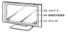
図16は、上記実施の形態の表示装置1,2が適用されるテレビジョン装置の外観を表したものである。このテレビジョン装置は、例えば、フロントパネル310およびフィルターガラス320を含む映像表示画面部300を有しており、この映像表示画面部300は、上記各実施の形態に係る表示装置1により構成されている。
(Application example 1)
FIG. 16 illustrates an appearance of a television device to which the display devices 1 and 2 according to the above embodiments are applied. The television apparatus has, for example, a video display screen unit 300 including a front panel 310 and a filter glass 320. The video display screen unit 300 is configured by the display device 1 according to each of the above embodiments. Yes.
(適用例2)
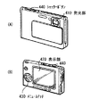
図17は、上記実施の形態の表示装置1,2が適用されるデジタルカメラの外観を表したものである。このデジタルカメラは、例えば、フラッシュ用の発光部410、表示部420、メニュースイッチ430およびシャッターボタン440を有しており、その表示部420は、上記各実施の形態に係る表示装置1により構成されている。
(Application example 2)
FIG. 17 illustrates the appearance of a digital camera to which the display devices 1 and 2 according to the above-described embodiments are applied. The digital camera includes, for example, a flash light emitting unit 410, a display unit 420, a menu switch 430, and a
(適用例3)
図18は、上記実施の形態の表示装置1,2が適用されるノート型パーソナルコンピュータの外観を表したものである。このノート型パーソナルコンピュータは、例えば、本体510,文字等の入力操作のためのキーボード520および画像を表示する表示部530を有しており、その表示部530は、上記各実施の形態に係る表示装置1により構成されている。
(Application example 3)
FIG. 18 shows the appearance of a notebook personal computer to which the display devices 1 and 2 of the above embodiment are applied. The notebook personal computer has, for example, a
(適用例4)
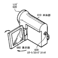
図19は、上記実施の形態の表示装置1,2が適用されるビデオカメラの外観を表したものである。このビデオカメラは、例えば、本体部610,この本体部610の前方側面に設けられた被写体撮影用のレンズ620,撮影時のスタート/ストップスイッチ630および表示部640を有しており、その表示部640は、上記各実施の形態に係る表示装置1により構成されている。
(Application example 4)
FIG. 19 shows the appearance of a video camera to which the display devices 1 and 2 of the above embodiment are applied. This video camera has, for example, a main body 610, a subject photographing lens 620 provided on the front side surface of the main body 610, a start /
(適用例5)
図20は、上記実施の形態の表示装置1,2が適用される携帯電話機の外観を表したものである。この携帯電話機は、例えば、上側筐体710と下側筐体720とを連結部(ヒンジ部)730で連結したものであり、ディスプレイ740,サブディスプレイ750,ピクチャーライト760およびカメラ770を有している。そのディスプレイ740またはサブディスプレイ750は、上記各実施の形態に係る表示装置1により構成されている。
(Application example 5)
FIG. 20 shows an appearance of a mobile phone to which the display devices 1 and 2 according to the above embodiments are applied. For example, the mobile phone is obtained by connecting an
以上、実施の形態および変形例を挙げて本技術を説明したが、本技術は上記実施の形態等に限定されるものではなく、種々変形が可能である。例えば、上記実施の形態等において説明した各層の材料および厚み、または成膜方法および成膜条件等は限定されるものではなく、他の材料および厚みとしてもよく、または他の成膜方法および成膜条件としてもよい。 Although the present technology has been described with the embodiment and the modification, the present technology is not limited to the above-described embodiment and the like, and various modifications can be made. For example, the material and thickness of each layer described in the above embodiment and the like, or the film formation method and film formation conditions are not limited, and other materials and thicknesses may be used. It is good also as film | membrane conditions.
また、上記実施の形態等においては、有機層16の発光層16Cとして赤色発光層16CR,緑色発光層16CGおよび青色発光層16CBの3層を含む白色発光用の発光層を形成した場合について説明したが、白色発光用の発光層16Cの構成は特に限定されず、橙色発光層および青色発光層、あるいは、青緑色発光層および赤色発光層など、互いに補色関係にある2色の発光層を積層した構造としてもよい。加えて、発光層16Cは、白色発光用の発光層に限らず、例えば緑色発光層16CGのみを形成した単色の表示装置にも適用可能である。
Further, in the above-described embodiment and the like, the case where the light emitting layer for white light emission including the red light emitting layer 16CR, the green light emitting layer 16CG, and the blue light emitting layer 16CB is formed as the light emitting layer 16C of the
更にまた、例えば上記実施の形態等では、第1電極14を陽極、第2電極17を陰極とする場合について説明したが、陽極および陰極を逆にして、第1電極14を陰極、第2電極17を陽極としてもよい。この場合、第2電極17の材料としては、金,銀,白金,銅等の単体あるいは合金が好適であるが、第2電極17の表面に適切なコーティングをすることにより他の材料を用いることも可能である。また、第1電極14を陰極、第2電極17を陽極とした場合には、発光層16Cは、第2電極17の側から順に赤色発光層16CR,緑色発光層16CGおよび青色発光層16CBが積層されていることが好ましい。
Furthermore, for example, in the above-described embodiment, the case where the
なお、本技術は以下のような構成も取ることができる。
(1)第1電極および第2電極と、前記第1電極と前記第2電極との間の、発光層を含む有機層と、前記第1電極の周縁を表面から側面にかけて覆うと共に前記有機層に接する内壁面を有し、前記内壁面に、稜線が前記第1電極の表面に平行な少なくとも一つの角部を有する絶縁膜とを備えた有機発光素子。
(2)前記絶縁膜の内壁面は前記稜線を境とした複数の面により構成され、前記複数の面の前記第1電極の表面に対する傾斜角度が互いに異なる前記(1)に記載の有機発光素子。
(3)前記絶縁膜の複数の面の各傾斜角度は、前記第2電極側から前記第1電極側に近づくにつれて大きくなる前記(1)または(2)に記載の有機発光素子。
(4)前記絶縁膜は1の角部を有し、前記内壁面のうち前記第1電極側の面の前記第1電極の表面とのなす角度は、70°以上90°未満である前記(1)乃至(3)のうちいずれか1つに記載の有機発光素子。
(5)前記内壁面のうち前記第2電極側の面の前記第1電極の表面とのなす角度は、20°以上45°以下である前記(1)乃至(4)のうちいずれか1つに記載の有機発光素子。
(6)前記絶縁膜は、酸窒化シリコン(SiON)からなる前記(1)乃至(5)のうちいずれか1つに記載の有機発光素子。
(7)前記角部は絶縁膜に対する逆スパッタリング処理により形成されたものである前記(1)乃至(6)のうちいずれか1つに記載の有機発光素子。
(8)第1電極および第2電極と、前記第1電極と前記第2電極との間の、発光層を含む有機層と、前記第1電極の側面を覆うと共に、前記側面の上端から下端にかけて傾斜面を有する絶縁膜とを備えた有機発光素子。
(9)前記第1電極、第2電極および有機層は基板上に設けられ、前記基板と前記傾斜面とのなす角度は、70°以下である前記(8)に記載の有機発光素子。
(10)前記基板と前記傾斜面とのなす角度は、30°以上60°以下である前記(9)に記載の有機発光素子。
(11)前記基板と前記第1電極との間に平坦化層が設けられ、前記傾斜面は前記平坦化層に接する前記(9)または(10)に記載の有機発光素子。
(12)前記第1電極、第2電極および有機層は基板上に設けられ、前記基板と前記第1電極の側面とのなす角度は、80°以上90°以下である前記(8)乃至(11)のうちいずれか1つに記載の有機発光素子。
(13)複数の有機発光素子を備え、前記有機発光素子は、第1電極および第2電極と、
前記第1電極と前記第2電極との間の、発光層を含む有機層と、前記第1電極の周縁を表面から側面にかけて覆うと共に前記有機層に接する内壁面を有し、前記内壁面に、稜線が前記第1電極の表面に平行な少なくとも一つの角部を有する絶縁膜とを備えた表示装置。
(14)複数の有機発光素子を備え、前記有機発光素子は、第1電極および第2電極と、前記第1電極と前記第2電極との間の、発光層を含む有機層と、前記第1電極の側面を覆うと共に、前記側面の上端から下端にかけて傾斜面を有する絶縁膜とを備えた表示装置。
In addition, this technique can also take the following structures.
(1) The first electrode and the second electrode, the organic layer including the light emitting layer between the first electrode and the second electrode, and the organic layer covering the periphery of the first electrode from the surface to the side surface. An organic light emitting device comprising an inner wall surface in contact with an insulating film having at least one corner portion whose ridge line is parallel to the surface of the first electrode.
(2) The organic light emitting element according to (1), wherein an inner wall surface of the insulating film is configured by a plurality of surfaces with the ridge line as a boundary, and the inclination angles of the plurality of surfaces with respect to the surface of the first electrode are different from each other. .
(3) The organic light-emitting element according to (1) or (2), wherein each inclination angle of the plurality of surfaces of the insulating film increases from the second electrode side toward the first electrode side.
(4) The insulating film has one corner, and an angle formed by a surface on the first electrode side of the inner wall surface with the surface of the first electrode is 70 ° or more and less than 90 ° ( The organic light-emitting device according to any one of 1) to (3).
(5) The angle formed by the surface on the second electrode side of the inner wall surface with the surface of the first electrode is 20 ° or more and 45 ° or less, and any one of (1) to (4). The organic light-emitting device described in 1.
(6) The organic light emitting element according to any one of (1) to (5), wherein the insulating film is made of silicon oxynitride (SiON).
(7) The organic light-emitting element according to any one of (1) to (6), wherein the corner portion is formed by a reverse sputtering process for an insulating film.
(8) The first electrode and the second electrode, the organic layer including the light emitting layer between the first electrode and the second electrode, and the side surface of the first electrode are covered, and the upper end to the lower end of the side surface And an insulating film having an inclined surface.
(9) The organic light-emitting element according to (8), wherein the first electrode, the second electrode, and the organic layer are provided on a substrate, and an angle formed by the substrate and the inclined surface is 70 ° or less.
(10) The organic light-emitting element according to (9), wherein an angle formed between the substrate and the inclined surface is 30 ° or more and 60 ° or less.
(11) The organic light-emitting element according to (9) or (10), wherein a planarization layer is provided between the substrate and the first electrode, and the inclined surface is in contact with the planarization layer.
(12) The first electrode, the second electrode, and the organic layer are provided on a substrate, and an angle formed between the substrate and a side surface of the first electrode is 80 ° or more and 90 ° or less. The organic light emitting element as described in any one of 11).
(13) It includes a plurality of organic light emitting elements, and the organic light emitting elements include a first electrode and a second electrode,
An organic layer including a light emitting layer between the first electrode and the second electrode, an inner wall surface covering the periphery of the first electrode from the surface to the side surface and in contact with the organic layer, A display device comprising: an insulating film having at least one corner whose ridgeline is parallel to the surface of the first electrode.
(14) A plurality of organic light emitting elements, wherein the organic light emitting element includes a first electrode and a second electrode, an organic layer including a light emitting layer between the first electrode and the second electrode, A display device including an insulating film that covers a side surface of one electrode and has an inclined surface from an upper end to a lower end of the side surface.
1,2・・・表示装置、10R,10G,10B・・・有機EL素子、11・・・基板、12・・・駆動回路層、13・・・平坦化層、14・・・第1電極、15,25・・・絶縁膜、15A・・・内壁面、15A1,15A2,15A3・・・面、15B,15B1,15B2・・・角部、16・・・有機層、17・・・第2電極、18・・・保護膜、20・・・封止パネル、21・・・封止用基板、22・・・カラーフィルタ、30・・・接着層。
DESCRIPTION OF SYMBOLS 1, 2 ... Display apparatus, 10R, 10G, 10B ... Organic EL element, 11 ... Board | substrate, 12 ... Drive circuit layer, 13 ... Planarization layer, 14 ... 1st electrode , 15, 25 ... insulating film, 15A ...
Claims (8)
前記第1電極と前記第2電極との間の、発光層を含む有機層と、
前記第1電極の周縁を表面から側面にかけて覆うと共に前記有機層に接する内壁面を有し、前記内壁面に、稜線が前記第1電極の表面に平行な少なくとも一つの角部を有する絶縁膜とを備え、
前記内壁面のうち前記第1電極側の第1面の前記第1電極の表面とのなす角度は、70°以上90°未満であり、
前記内壁面のうち前記第2電極側の第2面の前記第1電極の表面とのなす角度は、20°以上45°以下である
有機発光素子。 A first electrode and a second electrode;
An organic layer including a light emitting layer between the first electrode and the second electrode;
An insulating film that covers the periphery of the first electrode from the surface to the side surface and has an inner wall surface that is in contact with the organic layer, the inner wall surface having at least one corner whose ridge line is parallel to the surface of the first electrode; equipped with a,
The angle formed by the surface of the first electrode on the first electrode side of the inner wall surface is 70 ° or more and less than 90 °,
An organic light-emitting element in which an angle between a second surface on the second electrode side of the inner wall surface and a surface of the first electrode is 20 ° or more and 45 ° or less .
請求項1に記載の有機発光素子。 The inner wall surface of the insulating film is composed of a plurality of surfaces including at least the first surface and the second surface with the ridge line as a boundary, and the inclination angles of the plurality of surfaces with respect to the surface of the first electrode are different from each other. The organic light emitting device according to claim 1.
請求項2に記載の有機発光素子。 The inclination oblique angles of a plurality of surfaces of the insulating film, the organic light emitting device according to claim 2 from the second surface increases as it approaches the first surface.
前記絶縁膜の内壁面は、前記第1面と前記第2面との間に第3面を有するThe inner wall surface of the insulating film has a third surface between the first surface and the second surface.
請求項2に記載の有機発光素子。The organic light emitting device according to claim 2.
請求項4に記載の有機発光素子。The organic light emitting device according to claim 4.
請求項1ないし5のうちいずれか1つに記載の有機発光素子。 The organic light emitting element according to claim 1, wherein the insulating film is made of silicon oxynitride (SiON).
前記第1電極の周縁を表面から側面にかけて覆う絶縁膜を形成し、Forming an insulating film covering the periphery of the first electrode from the surface to the side surface;
前記第1電極との間に、発光層を含む有機層を設けて第2電極を形成し、An organic layer including a light emitting layer is provided between the first electrode and a second electrode is formed.
前記絶縁膜の形成では、前記有機層に接する内壁面を形成するとともに、前記内壁面に、稜線が前記第1電極の表面に平行な少なくとも一つの角部を形成し、In the formation of the insulating film, an inner wall surface in contact with the organic layer is formed, and at least one corner portion having a ridge line parallel to the surface of the first electrode is formed on the inner wall surface,
前記角部を前記絶縁膜に対する逆スパッタリング処理により形成して、前記内壁面のうち前記第1電極側の第1面の前記第1電極の表面とのなす角度を、70°以上90°未満とし、前記内壁面のうち前記第2電極側の第2面の前記第1電極の表面とのなす角度を、20°以上45°以下とするThe corner portion is formed by a reverse sputtering process on the insulating film, and an angle formed by the surface of the first electrode on the first electrode side of the inner wall surface with the surface of the first electrode is set to 70 ° or more and less than 90 °. The angle formed between the second electrode-side second surface of the inner wall surface and the surface of the first electrode is 20 ° to 45 °.
有機発光素子の製造方法。Manufacturing method of organic light emitting element.
前記有機発光素子は、
第1電極および第2電極と、
前記第1電極と前記第2電極との間の、発光層を含む有機層と、
前記第1電極の周縁を表面から側面にかけて覆うと共に前記有機層に接する内壁面を有し、前記内壁面に、稜線が前記第1電極の表面に平行な少なくとも一つの角部を有する絶縁膜とを備え、
前記内壁面のうち前記第1電極側の第1面の前記第1電極の表面とのなす角度は、70°以上90°未満であり、
前記内壁面のうち前記第2電極側の第2面の前記第1電極の表面とのなす角度は、20°以上45°以下である
表示装置。 Comprising a plurality of organic light emitting elements,
The organic light emitting device is
A first electrode and a second electrode;
An organic layer including a light emitting layer between the first electrode and the second electrode;
An insulating film that covers the periphery of the first electrode from the surface to the side surface and has an inner wall surface that is in contact with the organic layer, the inner wall surface having at least one corner whose ridge line is parallel to the surface of the first electrode; Bei to give a,
The angle formed by the surface of the first electrode on the first electrode side of the inner wall surface is 70 ° or more and less than 90 °,
A display device in which an angle formed between the second electrode-side second surface of the inner wall surface and the surface of the first electrode is 20 ° or more and 45 ° or less .
Priority Applications (5)
| Application Number | Priority Date | Filing Date | Title |
|---|---|---|---|
| JP2011281214A JP5919807B2 (en) | 2011-03-30 | 2011-12-22 | ORGANIC LIGHT EMITTING ELEMENT, METHOD FOR MANUFACTURING ORGANIC LIGHT EMITTING ELEMENT, AND DISPLAY DEVICE |
| US13/413,054 US8963170B2 (en) | 2011-03-30 | 2012-03-06 | Organic light emitting device and display unit including the same |
| CN201610108325.0A CN105590956B (en) | 2011-03-30 | 2012-03-23 | Organic light emitting device and display unit including the same |
| CN201210080412.1A CN102738406B (en) | 2011-03-30 | 2012-03-23 | Organic luminescent device and the display unit including organic luminescent device |
| US14/546,414 US9190460B2 (en) | 2011-03-30 | 2014-11-18 | Organic light emitting device and display unit including the same |
Applications Claiming Priority (3)
| Application Number | Priority Date | Filing Date | Title |
|---|---|---|---|
| JP2011075724 | 2011-03-30 | ||
| JP2011075724 | 2011-03-30 | ||
| JP2011281214A JP5919807B2 (en) | 2011-03-30 | 2011-12-22 | ORGANIC LIGHT EMITTING ELEMENT, METHOD FOR MANUFACTURING ORGANIC LIGHT EMITTING ELEMENT, AND DISPLAY DEVICE |
Publications (3)
| Publication Number | Publication Date |
|---|---|
| JP2012216495A JP2012216495A (en) | 2012-11-08 |
| JP2012216495A5 JP2012216495A5 (en) | 2014-12-25 |
| JP5919807B2 true JP5919807B2 (en) | 2016-05-18 |
Family
ID=46926045
Family Applications (1)
| Application Number | Title | Priority Date | Filing Date |
|---|---|---|---|
| JP2011281214A Expired - Fee Related JP5919807B2 (en) | 2011-03-30 | 2011-12-22 | ORGANIC LIGHT EMITTING ELEMENT, METHOD FOR MANUFACTURING ORGANIC LIGHT EMITTING ELEMENT, AND DISPLAY DEVICE |
Country Status (3)
| Country | Link |
|---|---|
| US (2) | US8963170B2 (en) |
| JP (1) | JP5919807B2 (en) |
| CN (2) | CN105590956B (en) |
Families Citing this family (37)
| Publication number | Priority date | Publication date | Assignee | Title |
|---|---|---|---|---|
| JP5919807B2 (en) * | 2011-03-30 | 2016-05-18 | ソニー株式会社 | ORGANIC LIGHT EMITTING ELEMENT, METHOD FOR MANUFACTURING ORGANIC LIGHT EMITTING ELEMENT, AND DISPLAY DEVICE |
| JP5535147B2 (en) | 2011-08-03 | 2014-07-02 | 株式会社ジャパンディスプレイ | Display device and manufacturing method of display device |
| JP5919723B2 (en) * | 2011-10-19 | 2016-05-18 | ソニー株式会社 | Display panel, display device and electronic device |
| JP5972566B2 (en) * | 2011-12-20 | 2016-08-17 | ピクストロニクス,インコーポレイテッド | Display device and manufacturing method thereof |
| JP6124584B2 (en) * | 2012-12-21 | 2017-05-10 | 株式会社半導体エネルギー研究所 | Light emitting device and manufacturing method thereof |
| JP2014154566A (en) * | 2013-02-04 | 2014-08-25 | Toshiba Corp | Organic electroluminescent element, illumination device and illumination system |
| JP6216125B2 (en) * | 2013-02-12 | 2017-10-18 | 株式会社半導体エネルギー研究所 | Light emitting device |
| WO2014155691A1 (en) * | 2013-03-29 | 2014-10-02 | 富士通セミコンダクター株式会社 | Semiconductor device and method for manufacturing same |
| JP6136578B2 (en) * | 2013-05-29 | 2017-05-31 | ソニー株式会社 | DISPLAY DEVICE, DISPLAY DEVICE MANUFACTURING METHOD, AND ELECTRONIC DEVICE |
| JP6119437B2 (en) * | 2013-06-05 | 2017-04-26 | セイコーエプソン株式会社 | Electro-optical device, method of manufacturing electro-optical device, and electronic apparatus |
| JP6282428B2 (en) * | 2013-09-09 | 2018-02-21 | 株式会社ジャパンディスプレイ | Organic electroluminescence display device and manufacturing method thereof |
| JP6207367B2 (en) * | 2013-12-05 | 2017-10-04 | 株式会社ジャパンディスプレイ | Organic electroluminescence display device |
| KR102331566B1 (en) * | 2014-12-31 | 2021-11-26 | 삼성디스플레이 주식회사 | Light emitting display device |
| JP6560530B2 (en) * | 2015-04-30 | 2019-08-14 | 株式会社ジャパンディスプレイ | Display device |
| US10243175B2 (en) * | 2016-02-02 | 2019-03-26 | Samsung Display Co., Ltd. | Organic light-emitting apparatus fabricated using a fluoropolymer and method of manufacturing the same |
| CN107665948B (en) * | 2016-07-27 | 2019-04-30 | 上海和辉光电有限公司 | Display panel, organic luminescent assembly and preparation method thereof |
| US20180151830A1 (en) * | 2016-11-30 | 2018-05-31 | Canon Kabushiki Kaisha | Display device and electronic device |
| JP6823443B2 (en) * | 2016-12-07 | 2021-02-03 | キヤノン株式会社 | Display device and its manufacturing method |
| JP2018190551A (en) * | 2017-04-28 | 2018-11-29 | キヤノン株式会社 | Organic light emitting device, imaging device, and method of manufacturing organic light emitting device |
| JP2017162832A (en) * | 2017-05-08 | 2017-09-14 | ソニー株式会社 | Display device and electronic apparatus |
| CN108091772B (en) * | 2017-06-27 | 2019-09-20 | 云谷(固安)科技有限公司 | OLED display unit and display panel |
| KR102083459B1 (en) * | 2017-11-30 | 2020-03-04 | 엘지디스플레이 주식회사 | Display Device and Eyeglasses type Augmented Reality Device |
| KR102095910B1 (en) * | 2017-12-13 | 2020-04-01 | 엘지디스플레이 주식회사 | Curved display device and method for fabricating the same |
| JP7057147B2 (en) | 2018-01-31 | 2022-04-19 | ソニーセミコンダクタソリューションズ株式会社 | Light emitting element and display device |
| DE112019005892T5 (en) | 2018-11-27 | 2021-08-05 | Sony Corporation | LIGHT EMITTING ELEMENT, DISPLAY DEVICE AND ELECTRONIC DEVICE |
| JP7444070B2 (en) | 2018-11-30 | 2024-03-06 | ソニーグループ株式会社 | display device |
| JPWO2020145148A1 (en) | 2019-01-08 | 2021-11-18 | ソニーセミコンダクタソリューションズ株式会社 | Display device |
| CN113383610A (en) | 2019-02-08 | 2021-09-10 | 索尼集团公司 | Light-emitting element and display device |
| JP2020136145A (en) | 2019-02-22 | 2020-08-31 | キヤノン株式会社 | Organic el element and light-emitting device |
| CN110299389B (en) * | 2019-06-26 | 2021-06-04 | 合肥视涯技术有限公司 | Organic light emitting display device |
| JP7341798B2 (en) * | 2019-08-30 | 2023-09-11 | キヤノン株式会社 | Semiconductor devices, light emitting devices, display devices, imaging devices, electronic equipment, lighting devices, and moving objects |
| JP2021039183A (en) | 2019-08-30 | 2021-03-11 | キヤノン株式会社 | Semiconductor device, display device, and photoelectric conversion device |
| TW202137598A (en) | 2020-02-26 | 2021-10-01 | 日商索尼半導體解決方案公司 | Light-emitting element and display device, and method for manufacutring display device |
| KR20210114595A (en) * | 2020-03-10 | 2021-09-24 | 삼성디스플레이 주식회사 | Display device |
| CN114639793A (en) * | 2020-12-16 | 2022-06-17 | 京东方科技集团股份有限公司 | Display substrate, preparation method thereof and display device |
| JPWO2022189908A1 (en) * | 2021-03-11 | 2022-09-15 | ||
| WO2023053450A1 (en) * | 2021-10-01 | 2023-04-06 | シャープディスプレイテクノロジー株式会社 | Light-emitting element, display device, and method for manufacturing light-emitting element |
Family Cites Families (24)
| Publication number | Priority date | Publication date | Assignee | Title |
|---|---|---|---|---|
| JP3691313B2 (en) | 1998-12-01 | 2005-09-07 | 三洋電機株式会社 | Display device |
| JP2000252078A (en) * | 1998-12-28 | 2000-09-14 | Toyota Motor Corp | El display element and its manufacture |
| JP2001110575A (en) | 1999-10-04 | 2001-04-20 | Sanyo Electric Co Ltd | Electroluminescence display apparatus |
| JP2004145244A (en) * | 2002-01-25 | 2004-05-20 | Semiconductor Energy Lab Co Ltd | Display device |
| KR100474906B1 (en) * | 2002-06-07 | 2005-03-10 | 엘지전자 주식회사 | Active Matrix Organic Electro-Luminescence Device |
| JP4321059B2 (en) * | 2002-12-16 | 2009-08-26 | 株式会社日立製作所 | Image display element and manufacturing method thereof |
| US7816863B2 (en) * | 2003-09-12 | 2010-10-19 | Semiconductor Energy Laboratory Co., Ltd. | Light emitting device and method for manufacturing the same |
| JP2005108825A (en) * | 2003-09-12 | 2005-04-21 | Semiconductor Energy Lab Co Ltd | Light emitting apparatus and method of manufacturing the same |
| JP4446771B2 (en) * | 2004-03-23 | 2010-04-07 | 株式会社リコー | Semiconductor device |
| US7753751B2 (en) * | 2004-09-29 | 2010-07-13 | Semiconductor Energy Laboratory Co., Ltd. | Method of fabricating the display device |
| JP4555727B2 (en) * | 2005-04-22 | 2010-10-06 | 株式会社 日立ディスプレイズ | Organic light emitting display |
| JP2009004347A (en) | 2007-05-18 | 2009-01-08 | Toppan Printing Co Ltd | Manufacturing method for organic el display element and organic el display element |
| EP2077698B1 (en) * | 2007-05-31 | 2011-09-07 | Panasonic Corporation | Organic el device and method for manufacturing the same |
| KR100943948B1 (en) * | 2008-01-08 | 2010-02-26 | 삼성모바일디스플레이주식회사 | Display device |
| JP4678421B2 (en) * | 2008-05-16 | 2011-04-27 | ソニー株式会社 | Display device |
| JP4975064B2 (en) * | 2008-05-28 | 2012-07-11 | パナソニック株式会社 | Light emitting device and manufacturing method thereof |
| WO2009147838A1 (en) * | 2008-06-06 | 2009-12-10 | パナソニック株式会社 | Organic el display panel and manufacturing method thereof |
| KR101572084B1 (en) * | 2008-07-16 | 2015-11-26 | 삼성디스플레이 주식회사 | Organic light emitting display and manufacturing method thereof |
| KR101460653B1 (en) * | 2008-07-23 | 2014-11-12 | 삼성디스플레이 주식회사 | Organic light emitting display and method of manufacuring the same |
| KR101073561B1 (en) * | 2009-02-05 | 2011-10-17 | 삼성모바일디스플레이주식회사 | organic electro luminescence display and method for fabricating the same |
| JP2010282807A (en) * | 2009-06-04 | 2010-12-16 | Casio Computer Co Ltd | Light-emitting panel |
| JP2010282899A (en) * | 2009-06-05 | 2010-12-16 | Panasonic Corp | Organic el device and method of manufacturing the same |
| KR101743789B1 (en) * | 2010-10-15 | 2017-06-05 | 가부시키가이샤 제이올레드 | Organic light emitting panel, method of manufacturing the same and organic display device |
| JP5919807B2 (en) * | 2011-03-30 | 2016-05-18 | ソニー株式会社 | ORGANIC LIGHT EMITTING ELEMENT, METHOD FOR MANUFACTURING ORGANIC LIGHT EMITTING ELEMENT, AND DISPLAY DEVICE |
-
2011
- 2011-12-22 JP JP2011281214A patent/JP5919807B2/en not_active Expired - Fee Related
-
2012
- 2012-03-06 US US13/413,054 patent/US8963170B2/en active Active
- 2012-03-23 CN CN201610108325.0A patent/CN105590956B/en active Active
- 2012-03-23 CN CN201210080412.1A patent/CN102738406B/en active Active
-
2014
- 2014-11-18 US US14/546,414 patent/US9190460B2/en active Active
Also Published As
| Publication number | Publication date |
|---|---|
| US9190460B2 (en) | 2015-11-17 |
| CN105590956A (en) | 2016-05-18 |
| JP2012216495A (en) | 2012-11-08 |
| CN102738406A (en) | 2012-10-17 |
| CN102738406B (en) | 2016-08-24 |
| CN105590956B (en) | 2020-11-06 |
| US20150069375A1 (en) | 2015-03-12 |
| US8963170B2 (en) | 2015-02-24 |
| US20120248467A1 (en) | 2012-10-04 |
Similar Documents
| Publication | Publication Date | Title |
|---|---|---|
| JP5919807B2 (en) | ORGANIC LIGHT EMITTING ELEMENT, METHOD FOR MANUFACTURING ORGANIC LIGHT EMITTING ELEMENT, AND DISPLAY DEVICE | |
| KR102056020B1 (en) | Display device | |
| JP6136578B2 (en) | DISPLAY DEVICE, DISPLAY DEVICE MANUFACTURING METHOD, AND ELECTRONIC DEVICE | |
| KR102376135B1 (en) | Display unit and electronic apparatus | |
| JP4655102B2 (en) | Display element, manufacturing method thereof, and display device | |
| KR101638194B1 (en) | Method of manufacturing display device and display device | |
| US11088355B2 (en) | Display unit with prevented current leakage, method of manufacturing the same, and method of manufacturing electronic apparatus | |
| JP2015128003A (en) | Display device and electronic apparatus | |
| TW200950584A (en) | Display unit | |
| JP2014199739A5 (en) | ||
| JP2008225179A (en) | Display device, driving method of the display device, and electronic apparatus | |
| JP2010062067A (en) | Method of manufacturing display device, and display device | |
| JP4924329B2 (en) | Method for manufacturing light emitting device | |
| JP5218489B2 (en) | Display element and manufacturing method thereof, display device and manufacturing method thereof | |
| JP4639588B2 (en) | Electro-optical device and method for manufacturing electro-optical device | |
| JP2017162832A (en) | Display device and electronic apparatus | |
| JP2011081998A (en) | Method for manufacturing organic el element, organic el element, and display device for the element |
Legal Events
| Date | Code | Title | Description |
|---|---|---|---|
| A521 | Request for written amendment filed |
Free format text: JAPANESE INTERMEDIATE CODE: A523 Effective date: 20141111 |
|
| A621 | Written request for application examination |
Free format text: JAPANESE INTERMEDIATE CODE: A621 Effective date: 20141111 |
|
| A977 | Report on retrieval |
Free format text: JAPANESE INTERMEDIATE CODE: A971007 Effective date: 20150810 |
|
| A131 | Notification of reasons for refusal |
Free format text: JAPANESE INTERMEDIATE CODE: A131 Effective date: 20150818 |
|
| A521 | Request for written amendment filed |
Free format text: JAPANESE INTERMEDIATE CODE: A523 Effective date: 20151007 |
|
| TRDD | Decision of grant or rejection written | ||
| A01 | Written decision to grant a patent or to grant a registration (utility model) |
Free format text: JAPANESE INTERMEDIATE CODE: A01 Effective date: 20160315 |
|
| A61 | First payment of annual fees (during grant procedure) |
Free format text: JAPANESE INTERMEDIATE CODE: A61 Effective date: 20160328 |
|
| R151 | Written notification of patent or utility model registration |
Ref document number: 5919807 Country of ref document: JP Free format text: JAPANESE INTERMEDIATE CODE: R151 |
|
| R250 | Receipt of annual fees |
Free format text: JAPANESE INTERMEDIATE CODE: R250 |
|
| R250 | Receipt of annual fees |
Free format text: JAPANESE INTERMEDIATE CODE: R250 |
|
| LAPS | Cancellation because of no payment of annual fees |