JP5919087B2 - Semiconductor device manufacturing method and semiconductor device - Google Patents
Semiconductor device manufacturing method and semiconductor device Download PDFInfo
- Publication number
- JP5919087B2 JP5919087B2 JP2012108266A JP2012108266A JP5919087B2 JP 5919087 B2 JP5919087 B2 JP 5919087B2 JP 2012108266 A JP2012108266 A JP 2012108266A JP 2012108266 A JP2012108266 A JP 2012108266A JP 5919087 B2 JP5919087 B2 JP 5919087B2
- Authority
- JP
- Japan
- Prior art keywords
- resist film
- back surface
- semiconductor device
- leads
- region
- Prior art date
- Legal status (The legal status is an assumption and is not a legal conclusion. Google has not performed a legal analysis and makes no representation as to the accuracy of the status listed.)
- Expired - Fee Related
Links
Images


Classifications
-
- H—ELECTRICITY
- H10—SEMICONDUCTOR DEVICES; ELECTRIC SOLID-STATE DEVICES NOT OTHERWISE PROVIDED FOR
- H10W—GENERIC PACKAGES, INTERCONNECTIONS, CONNECTORS OR OTHER CONSTRUCTIONAL DETAILS OF DEVICES COVERED BY CLASS H10
- H10W42/00—Arrangements for protection of devices
- H10W42/121—Arrangements for protection of devices protecting against mechanical damage
-
- H—ELECTRICITY
- H10—SEMICONDUCTOR DEVICES; ELECTRIC SOLID-STATE DEVICES NOT OTHERWISE PROVIDED FOR
- H10P—GENERIC PROCESSES OR APPARATUS FOR THE MANUFACTURE OR TREATMENT OF DEVICES COVERED BY CLASS H10
- H10P54/00—Cutting or separating of wafers, substrates or parts of devices
-
- H—ELECTRICITY
- H10—SEMICONDUCTOR DEVICES; ELECTRIC SOLID-STATE DEVICES NOT OTHERWISE PROVIDED FOR
- H10P—GENERIC PROCESSES OR APPARATUS FOR THE MANUFACTURE OR TREATMENT OF DEVICES COVERED BY CLASS H10
- H10P72/00—Handling or holding of wafers, substrates or devices during manufacture or treatment thereof
- H10P72/70—Handling or holding of wafers, substrates or devices during manufacture or treatment thereof for supporting or gripping
- H10P72/74—Handling or holding of wafers, substrates or devices during manufacture or treatment thereof for supporting or gripping using temporarily an auxiliary support
- H10P72/7402—Wafer tapes, e.g. grinding or dicing support tapes
-
- H—ELECTRICITY
- H10—SEMICONDUCTOR DEVICES; ELECTRIC SOLID-STATE DEVICES NOT OTHERWISE PROVIDED FOR
- H10W—GENERIC PACKAGES, INTERCONNECTIONS, CONNECTORS OR OTHER CONSTRUCTIONAL DETAILS OF DEVICES COVERED BY CLASS H10
- H10W46/00—Marks applied to devices, e.g. for alignment or identification
-
- H—ELECTRICITY
- H10—SEMICONDUCTOR DEVICES; ELECTRIC SOLID-STATE DEVICES NOT OTHERWISE PROVIDED FOR
- H10W—GENERIC PACKAGES, INTERCONNECTIONS, CONNECTORS OR OTHER CONSTRUCTIONAL DETAILS OF DEVICES COVERED BY CLASS H10
- H10W70/00—Package substrates; Interposers; Redistribution layers [RDL]
- H10W70/01—Manufacture or treatment
- H10W70/04—Manufacture or treatment of leadframes
- H10W70/041—Connecting or disconnecting interconnections to or from leadframes, e.g. connecting bond wires or bumps
-
- H—ELECTRICITY
- H10—SEMICONDUCTOR DEVICES; ELECTRIC SOLID-STATE DEVICES NOT OTHERWISE PROVIDED FOR
- H10W—GENERIC PACKAGES, INTERCONNECTIONS, CONNECTORS OR OTHER CONSTRUCTIONAL DETAILS OF DEVICES COVERED BY CLASS H10
- H10W70/00—Package substrates; Interposers; Redistribution layers [RDL]
- H10W70/40—Leadframes
- H10W70/411—Chip-supporting parts, e.g. die pads
-
- H—ELECTRICITY
- H10—SEMICONDUCTOR DEVICES; ELECTRIC SOLID-STATE DEVICES NOT OTHERWISE PROVIDED FOR
- H10W—GENERIC PACKAGES, INTERCONNECTIONS, CONNECTORS OR OTHER CONSTRUCTIONAL DETAILS OF DEVICES COVERED BY CLASS H10
- H10W70/00—Package substrates; Interposers; Redistribution layers [RDL]
- H10W70/40—Leadframes
- H10W70/421—Shapes or dispositions
-
- H—ELECTRICITY
- H10—SEMICONDUCTOR DEVICES; ELECTRIC SOLID-STATE DEVICES NOT OTHERWISE PROVIDED FOR
- H10W—GENERIC PACKAGES, INTERCONNECTIONS, CONNECTORS OR OTHER CONSTRUCTIONAL DETAILS OF DEVICES COVERED BY CLASS H10
- H10W70/00—Package substrates; Interposers; Redistribution layers [RDL]
- H10W70/40—Leadframes
- H10W70/464—Additional interconnections in combination with leadframes
- H10W70/465—Bumps or wires
-
- H—ELECTRICITY
- H10—SEMICONDUCTOR DEVICES; ELECTRIC SOLID-STATE DEVICES NOT OTHERWISE PROVIDED FOR
- H10W—GENERIC PACKAGES, INTERCONNECTIONS, CONNECTORS OR OTHER CONSTRUCTIONAL DETAILS OF DEVICES COVERED BY CLASS H10
- H10W74/00—Encapsulations, e.g. protective coatings
- H10W74/01—Manufacture or treatment
- H10W74/014—Manufacture or treatment using batch processing
-
- H—ELECTRICITY
- H10—SEMICONDUCTOR DEVICES; ELECTRIC SOLID-STATE DEVICES NOT OTHERWISE PROVIDED FOR
- H10W—GENERIC PACKAGES, INTERCONNECTIONS, CONNECTORS OR OTHER CONSTRUCTIONAL DETAILS OF DEVICES COVERED BY CLASS H10
- H10W74/00—Encapsulations, e.g. protective coatings
- H10W74/01—Manufacture or treatment
- H10W74/016—Manufacture or treatment using moulds
-
- H—ELECTRICITY
- H10—SEMICONDUCTOR DEVICES; ELECTRIC SOLID-STATE DEVICES NOT OTHERWISE PROVIDED FOR
- H10W—GENERIC PACKAGES, INTERCONNECTIONS, CONNECTORS OR OTHER CONSTRUCTIONAL DETAILS OF DEVICES COVERED BY CLASS H10
- H10W74/00—Encapsulations, e.g. protective coatings
- H10W74/01—Manufacture or treatment
- H10W74/019—Manufacture or treatment using temporary auxiliary substrates
-
- H—ELECTRICITY
- H10—SEMICONDUCTOR DEVICES; ELECTRIC SOLID-STATE DEVICES NOT OTHERWISE PROVIDED FOR
- H10W—GENERIC PACKAGES, INTERCONNECTIONS, CONNECTORS OR OTHER CONSTRUCTIONAL DETAILS OF DEVICES COVERED BY CLASS H10
- H10W74/00—Encapsulations, e.g. protective coatings
- H10W74/10—Encapsulations, e.g. protective coatings characterised by their shape or disposition
- H10W74/111—Encapsulations, e.g. protective coatings characterised by their shape or disposition the semiconductor body being completely enclosed
- H10W74/129—Encapsulations, e.g. protective coatings characterised by their shape or disposition the semiconductor body being completely enclosed forming a chip-scale package [CSP]
-
- H—ELECTRICITY
- H10—SEMICONDUCTOR DEVICES; ELECTRIC SOLID-STATE DEVICES NOT OTHERWISE PROVIDED FOR
- H10W—GENERIC PACKAGES, INTERCONNECTIONS, CONNECTORS OR OTHER CONSTRUCTIONAL DETAILS OF DEVICES COVERED BY CLASS H10
- H10W74/00—Encapsulations, e.g. protective coatings
- H10W74/40—Encapsulations, e.g. protective coatings characterised by their materials
- H10W74/47—Encapsulations, e.g. protective coatings characterised by their materials comprising organic materials, e.g. plastics or resins
-
- H—ELECTRICITY
- H10—SEMICONDUCTOR DEVICES; ELECTRIC SOLID-STATE DEVICES NOT OTHERWISE PROVIDED FOR
- H10P—GENERIC PROCESSES OR APPARATUS FOR THE MANUFACTURE OR TREATMENT OF DEVICES COVERED BY CLASS H10
- H10P72/00—Handling or holding of wafers, substrates or devices during manufacture or treatment thereof
- H10P72/70—Handling or holding of wafers, substrates or devices during manufacture or treatment thereof for supporting or gripping
- H10P72/74—Handling or holding of wafers, substrates or devices during manufacture or treatment thereof for supporting or gripping using temporarily an auxiliary support
- H10P72/7416—Handling or holding of wafers, substrates or devices during manufacture or treatment thereof for supporting or gripping using temporarily an auxiliary support used during dicing or grinding
-
- H—ELECTRICITY
- H10—SEMICONDUCTOR DEVICES; ELECTRIC SOLID-STATE DEVICES NOT OTHERWISE PROVIDED FOR
- H10P—GENERIC PROCESSES OR APPARATUS FOR THE MANUFACTURE OR TREATMENT OF DEVICES COVERED BY CLASS H10
- H10P72/00—Handling or holding of wafers, substrates or devices during manufacture or treatment thereof
- H10P72/70—Handling or holding of wafers, substrates or devices during manufacture or treatment thereof for supporting or gripping
- H10P72/74—Handling or holding of wafers, substrates or devices during manufacture or treatment thereof for supporting or gripping using temporarily an auxiliary support
- H10P72/7422—Handling or holding of wafers, substrates or devices during manufacture or treatment thereof for supporting or gripping using temporarily an auxiliary support used to protect an active side of a device or wafer
-
- H—ELECTRICITY
- H10—SEMICONDUCTOR DEVICES; ELECTRIC SOLID-STATE DEVICES NOT OTHERWISE PROVIDED FOR
- H10P—GENERIC PROCESSES OR APPARATUS FOR THE MANUFACTURE OR TREATMENT OF DEVICES COVERED BY CLASS H10
- H10P72/00—Handling or holding of wafers, substrates or devices during manufacture or treatment thereof
- H10P72/70—Handling or holding of wafers, substrates or devices during manufacture or treatment thereof for supporting or gripping
- H10P72/74—Handling or holding of wafers, substrates or devices during manufacture or treatment thereof for supporting or gripping using temporarily an auxiliary support
- H10P72/744—Details of chemical or physical process used for separating the auxiliary support from a device or a wafer
-
- H—ELECTRICITY
- H10—SEMICONDUCTOR DEVICES; ELECTRIC SOLID-STATE DEVICES NOT OTHERWISE PROVIDED FOR
- H10W—GENERIC PACKAGES, INTERCONNECTIONS, CONNECTORS OR OTHER CONSTRUCTIONAL DETAILS OF DEVICES COVERED BY CLASS H10
- H10W46/00—Marks applied to devices, e.g. for alignment or identification
- H10W46/101—Marks applied to devices, e.g. for alignment or identification characterised by the type of information, e.g. logos or symbols
- H10W46/103—Marks applied to devices, e.g. for alignment or identification characterised by the type of information, e.g. logos or symbols alphanumeric information, e.g. words, letters or serial numbers
-
- H—ELECTRICITY
- H10—SEMICONDUCTOR DEVICES; ELECTRIC SOLID-STATE DEVICES NOT OTHERWISE PROVIDED FOR
- H10W—GENERIC PACKAGES, INTERCONNECTIONS, CONNECTORS OR OTHER CONSTRUCTIONAL DETAILS OF DEVICES COVERED BY CLASS H10
- H10W46/00—Marks applied to devices, e.g. for alignment or identification
- H10W46/301—Marks applied to devices, e.g. for alignment or identification for alignment
-
- H—ELECTRICITY
- H10—SEMICONDUCTOR DEVICES; ELECTRIC SOLID-STATE DEVICES NOT OTHERWISE PROVIDED FOR
- H10W—GENERIC PACKAGES, INTERCONNECTIONS, CONNECTORS OR OTHER CONSTRUCTIONAL DETAILS OF DEVICES COVERED BY CLASS H10
- H10W46/00—Marks applied to devices, e.g. for alignment or identification
- H10W46/401—Marks applied to devices, e.g. for alignment or identification for identification or tracking
-
- H—ELECTRICITY
- H10—SEMICONDUCTOR DEVICES; ELECTRIC SOLID-STATE DEVICES NOT OTHERWISE PROVIDED FOR
- H10W—GENERIC PACKAGES, INTERCONNECTIONS, CONNECTORS OR OTHER CONSTRUCTIONAL DETAILS OF DEVICES COVERED BY CLASS H10
- H10W46/00—Marks applied to devices, e.g. for alignment or identification
- H10W46/601—Marks applied to devices, e.g. for alignment or identification for use after dicing
- H10W46/607—Located on parts of packages, e.g. on encapsulations or on package substrates
-
- H—ELECTRICITY
- H10—SEMICONDUCTOR DEVICES; ELECTRIC SOLID-STATE DEVICES NOT OTHERWISE PROVIDED FOR
- H10W—GENERIC PACKAGES, INTERCONNECTIONS, CONNECTORS OR OTHER CONSTRUCTIONAL DETAILS OF DEVICES COVERED BY CLASS H10
- H10W72/00—Interconnections or connectors in packages
- H10W72/01—Manufacture or treatment
- H10W72/0198—Manufacture or treatment batch processes
-
- H—ELECTRICITY
- H10—SEMICONDUCTOR DEVICES; ELECTRIC SOLID-STATE DEVICES NOT OTHERWISE PROVIDED FOR
- H10W—GENERIC PACKAGES, INTERCONNECTIONS, CONNECTORS OR OTHER CONSTRUCTIONAL DETAILS OF DEVICES COVERED BY CLASS H10
- H10W72/00—Interconnections or connectors in packages
- H10W72/071—Connecting or disconnecting
- H10W72/0711—Apparatus therefor
- H10W72/07141—Means for applying energy, e.g. ovens or lasers
-
- H—ELECTRICITY
- H10—SEMICONDUCTOR DEVICES; ELECTRIC SOLID-STATE DEVICES NOT OTHERWISE PROVIDED FOR
- H10W—GENERIC PACKAGES, INTERCONNECTIONS, CONNECTORS OR OTHER CONSTRUCTIONAL DETAILS OF DEVICES COVERED BY CLASS H10
- H10W72/00—Interconnections or connectors in packages
- H10W72/071—Connecting or disconnecting
- H10W72/075—Connecting or disconnecting of bond wires
- H10W72/07521—Aligning
-
- H—ELECTRICITY
- H10—SEMICONDUCTOR DEVICES; ELECTRIC SOLID-STATE DEVICES NOT OTHERWISE PROVIDED FOR
- H10W—GENERIC PACKAGES, INTERCONNECTIONS, CONNECTORS OR OTHER CONSTRUCTIONAL DETAILS OF DEVICES COVERED BY CLASS H10
- H10W74/00—Encapsulations, e.g. protective coatings
-
- H—ELECTRICITY
- H10—SEMICONDUCTOR DEVICES; ELECTRIC SOLID-STATE DEVICES NOT OTHERWISE PROVIDED FOR
- H10W—GENERIC PACKAGES, INTERCONNECTIONS, CONNECTORS OR OTHER CONSTRUCTIONAL DETAILS OF DEVICES COVERED BY CLASS H10
- H10W74/00—Encapsulations, e.g. protective coatings
- H10W74/10—Encapsulations, e.g. protective coatings characterised by their shape or disposition
- H10W74/131—Encapsulations, e.g. protective coatings characterised by their shape or disposition the semiconductor body being only partially enclosed
- H10W74/142—Encapsulations, e.g. protective coatings characterised by their shape or disposition the semiconductor body being only partially enclosed the encapsulations exposing the passive side of the semiconductor body
-
- H—ELECTRICITY
- H10—SEMICONDUCTOR DEVICES; ELECTRIC SOLID-STATE DEVICES NOT OTHERWISE PROVIDED FOR
- H10W—GENERIC PACKAGES, INTERCONNECTIONS, CONNECTORS OR OTHER CONSTRUCTIONAL DETAILS OF DEVICES COVERED BY CLASS H10
- H10W90/00—Package configurations
- H10W90/701—Package configurations characterised by the relative positions of pads or connectors relative to package parts
- H10W90/751—Package configurations characterised by the relative positions of pads or connectors relative to package parts of bond wires
- H10W90/753—Package configurations characterised by the relative positions of pads or connectors relative to package parts of bond wires between laterally-adjacent chips
-
- H—ELECTRICITY
- H10—SEMICONDUCTOR DEVICES; ELECTRIC SOLID-STATE DEVICES NOT OTHERWISE PROVIDED FOR
- H10W—GENERIC PACKAGES, INTERCONNECTIONS, CONNECTORS OR OTHER CONSTRUCTIONAL DETAILS OF DEVICES COVERED BY CLASS H10
- H10W90/00—Package configurations
- H10W90/701—Package configurations characterised by the relative positions of pads or connectors relative to package parts
- H10W90/751—Package configurations characterised by the relative positions of pads or connectors relative to package parts of bond wires
- H10W90/756—Package configurations characterised by the relative positions of pads or connectors relative to package parts of bond wires between a chip and a stacked lead frame, conducting package substrate or heat sink
Landscapes
- Lead Frames For Integrated Circuits (AREA)
- Structures Or Materials For Encapsulating Or Coating Semiconductor Devices Or Solid State Devices (AREA)
- Encapsulation Of And Coatings For Semiconductor Or Solid State Devices (AREA)
- Engineering & Computer Science (AREA)
- Microelectronics & Electronic Packaging (AREA)
Description
本発明は半導体装置の製造技術および半導体装置に関し、例えばパッケージの裏面にリードを有する半導体装置の製造に好適に利用できるものである。 The present invention relates to a semiconductor device manufacturing technique and a semiconductor device, and can be suitably used for manufacturing a semiconductor device having leads on the back surface of a package, for example.
樹脂封止された半導体装置の特性選別においては、複数のリード(外部接続端子、外部端子、端子)のなかからインデックス(識別番号、通し番号、指標)として1番目のリードと定められた1pin(1ピン)の位置を認識する必要がある。 In selecting the characteristics of a resin-encapsulated semiconductor device, 1 pin (1 pin) defined as the first lead as an index (identification number, serial number, index) among a plurality of leads (external connection terminals, external terminals, terminals) It is necessary to recognize the position of the pin.
例えば特開2008−288304号公報(特許文献1)には、モールド樹脂の下面から露出する周辺部の吊りリードの先端部を補強端子部として構成し、1つの補強端子部を、他の補強端子部とはモールド樹脂から露出する形状が異なるものとすることにより、1pinを認識する技術が開示されている。 For example, Japanese Patent Application Laid-Open No. 2008-288304 (Patent Document 1) discloses that a distal end portion of a peripheral suspension lead exposed from the lower surface of a mold resin is configured as a reinforcing terminal portion, and one reinforcing terminal portion is replaced with another reinforcing terminal. A technique for recognizing 1 pin is disclosed by making the shape exposed from the mold resin different from the part.
また、特開2011−091145号公報(特許文献2)には、樹脂パッケージの裏面に露出するアイランドのコーナー部の一部を切り欠くことで、アイランドの露出形状が位置認識マークとして利用される技術が開示されている。 Japanese Patent Laid-Open No. 2011-091145 (Patent Document 2) discloses a technique in which an exposed shape of an island is used as a position recognition mark by cutting out a part of a corner portion of an island exposed on the back surface of a resin package. Is disclosed.
また、特開2006−229263号公報(特許文献3)には、樹脂封止体の裏面から複数の吊りリードの一部を露出させ、そのうちの1本を樹脂封止体の向きを認識するためのインデックスとして用いる技術が開示されている。 Japanese Patent Laid-Open No. 2006-229263 (Patent Document 3) discloses a method in which a part of a plurality of suspension leads is exposed from the back surface of a resin sealing body, and one of them is used to recognize the orientation of the resin sealing body. A technique used as an index for the above is disclosed.
また、特開2003−332513号公報(特許文献4)には、封止体の表面側の対角線方向に沿った2つのコーナー部に切り欠き部を設け、これら切り欠き部から、円形の平面形状を有する認識マークが設けられた吊りリードの一部を露出する技術が開示されている。 Japanese Patent Laying-Open No. 2003-332513 (Patent Document 4) provides notches at two corners along the diagonal direction on the surface side of the sealing body, and a circular planar shape is formed from these notches. A technique for exposing a part of a suspension lead provided with a recognition mark having a mark is disclosed.
また、特開2004−327903号公報(特許文献5)には、リードの一面をハーフエッチング面、他面を非ハーフエッチング面とし、非ハーフエッチング面と外側側面とを樹脂から露出させ、これ以外を樹脂中にして樹脂封止した半導体装置が開示されている。 Japanese Patent Laid-Open No. 2004-327903 (Patent Document 5) discloses that one surface of a lead is a half-etched surface, the other surface is a non-half-etched surface, and the non-half-etched surface and the outer side surface are exposed from the resin. A semiconductor device in which resin is sealed in resin is disclosed.
樹脂封止された半導体装置(半導体パッケージ)においては、その裏面から露出する複数のリードのなかから1個のリードを「1pin」と定めている。この1pinは、半導体装置の向きの識別、または検査時において複数のリードの各々を識別する役割を担う。そのため、外観から容易に1pinを認識できることが必要である。しかし、パーツフィーダ方式の特性選別を採用する場合、タブレスパッケージでは1pinの位置認識ができないという課題が生じていた。 In a resin-sealed semiconductor device (semiconductor package), one lead is defined as “1 pin” among a plurality of leads exposed from the back surface thereof. This 1 pin plays a role of identifying the orientation of the semiconductor device or identifying each of the plurality of leads at the time of inspection. Therefore, it is necessary that 1 pin can be easily recognized from the appearance. However, when adopting the characteristic selection of the parts feeder method, there is a problem that the position of 1 pin cannot be recognized in the tabless package.
その他の課題と新規な特徴は、本明細書の記述および添付図面から明らかになるであろう。 Other problems and novel features will become apparent from the description of the specification and the accompanying drawings.
一実施の形態によれば、吊りリードに連結され、樹脂封止体の裏面に露出する識別用目印を形成し、この識別用目印によって樹脂封止体の裏面に露出する複数のリードのなかから1pinの位置認識を行う。 According to one embodiment, the identification mark that is connected to the suspension lead and is exposed on the back surface of the resin sealing body is formed, and the plurality of leads that are exposed on the back surface of the resin sealing body by the identification mark. 1 pin position recognition is performed.
一実施の形態によれば、タブレスパッケージにおいて1pinの位置認識を容易に行うことができる。 According to one embodiment, it is possible to easily recognize the position of 1 pin in a tabless package.
以下の実施の形態において、便宜上その必要があるときは、複数のセクションまたは実施の形態に分割して説明するが、特に明示した場合を除き、それらはお互いに無関係なものではなく、一方は他方の一部または全部の変形例、詳細、補足説明等の関係にある。 In the following embodiments, when necessary for the sake of convenience, the description will be divided into a plurality of sections or embodiments. However, unless otherwise specified, they are not irrelevant to each other, and one is the other. There are some or all of the modifications, details, supplementary explanations, and the like.
また、以下の実施の形態において、要素の数等(個数、数値、量、範囲等を含む)に言及する場合、特に明示した場合および原理的に明らかに特定の数に限定される場合等を除き、その特定の数に限定されるものではなく、特定の数以上でも以下でも良い。さらに、以下の実施の形態において、その構成要素(要素ステップ等も含む)は、特に明示した場合および原理的に明らかに必須であると考えられる場合等を除き、必ずしも必須のものではないことは言うまでもない。同様に、以下の実施の形態において、構成要素等の形状、位置関係等に言及するときは、特に明示した場合および原理的に明らかにそうでないと考えられる場合等を除き、実質的にその形状等に近似または類似するもの等を含むものとする。このことは、上記数値および範囲についても同様である。 Further, in the following embodiments, when referring to the number of elements (including the number, numerical value, quantity, range, etc.), especially when clearly indicated and when clearly limited to a specific number in principle, etc. Except, it is not limited to the specific number, and may be more or less than the specific number. Further, in the following embodiments, the constituent elements (including element steps and the like) are not necessarily indispensable unless otherwise specified and apparently essential in principle. Needless to say. Similarly, in the following embodiments, when referring to the shapes, positional relationships, etc. of the components, etc., the shapes are substantially the same unless otherwise specified, or otherwise apparent in principle. And the like are included. The same applies to the above numerical values and ranges.
また、以下の実施の形態において、タブレスパッケージとは、半導体チップを搭載する基材(タブ、アイランド)がなく、半導体チップを封止する樹脂封止体の裏面(下面、底面)に上記基材が露出しない樹脂パッケージを言う。 In the following embodiments, a tabless package means that there is no substrate (tab, island) on which a semiconductor chip is mounted, and the above-mentioned base is provided on the back surface (lower surface, bottom surface) of a resin sealing body that seals the semiconductor chip. A resin package where the material is not exposed.
また、以下の実施の形態で用いる図面においては、平面図であっても図面を見易くするためにハッチングを付す場合もある。また、以下の実施の形態を説明するための全図において、同一機能を有するものは原則として同一の符号を付し、その繰り返しの説明は省略する。以下、本実施の形態を図面に基づいて詳細に説明する。 Further, in the drawings used in the following embodiments, hatching may be added to make the drawings easy to see even if they are plan views. In all the drawings for explaining the following embodiments, components having the same function are denoted by the same reference numerals in principle, and repeated description thereof is omitted. Hereinafter, the present embodiment will be described in detail with reference to the drawings.
(詳細な課題)
リードフレームに搭載された半導体チップを樹脂からなる封止体によって封止した半導体パッケージの一種にQFN(Quad Flat Non-leaded package)がある。
(Detailed issues)
One type of semiconductor package in which a semiconductor chip mounted on a lead frame is sealed with a sealing body made of resin is QFN (Quad Flat Non-leaded package).
QFNは、封止体の中央部に半導体チップを配置し、半導体チップの周囲に複数のリードを配置し、封止体の内部において半導体チップの表面に形成された複数の電極パッドと複数のリードの表面とを複数のボンディングワイヤを介してそれぞれ電気的に接続し、複数のリードの裏面を封止体の裏面から露出する構造となっている。そして、封止体の裏面から露出した複数のリードのそれぞれの裏面を配線基板の電極(フットプリント)に半田付けすることによって、半導体パッケージは実装される。このQFNは、複数のリードが封止体の側面から横方向に延びるQFP(Quad Flat Package)に比べて、実装面積が小さくなるという利点を備えている。 In QFN, a semiconductor chip is arranged at the center of a sealing body, a plurality of leads are arranged around the semiconductor chip, and a plurality of electrode pads and a plurality of leads formed on the surface of the semiconductor chip inside the sealing body. Are electrically connected to each other via a plurality of bonding wires, and the back surfaces of the plurality of leads are exposed from the back surface of the sealing body. The semiconductor package is mounted by soldering the back surfaces of the plurality of leads exposed from the back surface of the sealing body to the electrodes (footprints) of the wiring board. This QFN has an advantage that a mounting area is reduced as compared with a QFP (Quad Flat Package) in which a plurality of leads extend laterally from the side surface of the sealing body.
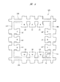
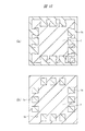
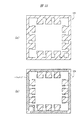
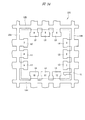
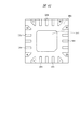
図58に、QFNの一例であるタブレスパッケージの裏面の要部平面図を示す。封止体MO1の外周部の裏面には、複数(24個)のリードLE1の裏面がそれぞれ露出している。図58中に示す数字は各リードLE1のインデックス(識別番号、通し番号、指標)であり、インデックス1に該当するリードLE1を「1pin」と言う。
FIG. 58 shows a plan view of the main part of the back surface of a tabless package which is an example of QFN. The back surfaces of a plurality of (24) leads LE1 are exposed on the back surface of the outer peripheral portion of the sealing body MO1. The numbers shown in FIG. 58 are indexes (identification numbers, serial numbers, indexes) of each lead LE1, and the lead LE1 corresponding to the
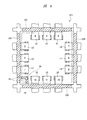
図59に、QFNの一例であるタブレスパッケージの第1変形例の裏面の要部平面図を示す。封止体MO2の外周部の裏面には、複数(20個)のリードLE2の裏面がそれぞれ露出している。前述の図58と同様に、図59中に示す数字は各リードLE2のインデックスであり、インデックス1に該当するリードLE2を「1pin」と言う。
FIG. 59 is a plan view of the main part of the back surface of the first modification of the tabless package, which is an example of QFN. On the back surface of the outer peripheral portion of the sealing body MO2, the back surfaces of the plural (20) leads LE2 are exposed. Similarly to FIG. 58 described above, the numbers shown in FIG. 59 are indexes of each lead LE2, and the lead LE2 corresponding to the
封止体MO2から露出した1pinの裏面における封止体MO2の外周に沿った方向の幅が、封止体MO2から露出した他のリードLE2の裏面における封止体MO2の外周に沿った幅よりも大きく形成されている。すなわち、この1pinの封止体MO2の裏面から露出する形状は、他のリードLE2の封止体MO2の裏面から露出する形状とは相違しており、これにより、1pinを認識することができる。 The width in the direction along the outer periphery of the sealing body MO2 on the back surface of 1 pin exposed from the sealing body MO2 is larger than the width along the outer periphery of the sealing body MO2 on the back surface of the other lead LE2 exposed from the sealing body MO2. Is also formed large. That is, the shape exposed from the back surface of the sealing body MO2 of 1 pin is different from the shape exposed from the back surface of the sealing body MO2 of the other lead LE2, and thus 1 pin can be recognized.
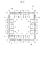
図60に、QFNの一例であるタブレスパッケージの第2変形例の裏面の要部平面図を示す。封止体MO3の外周部の裏面には、複数(16個)のリードLE3の裏面がそれぞれ露出している。前述の図58と同様に、図60中に示す数字は各リードLE3のインデックスであり、インデックス1に該当するリードLE3を「1pin」と言う。
FIG. 60 is a plan view of the main part of the back surface of the second modification of the tabless package which is an example of QFN. On the back surface of the outer peripheral portion of the sealing body MO3, the back surfaces of the plural (16) leads LE3 are exposed. Similarly to FIG. 58 described above, the numbers shown in FIG. 60 are the indexes of the respective leads LE3, and the lead LE3 corresponding to the
封止体MO3から露出した1pinの裏面における封止体MO3の外周に沿った方向と封止体MO3の裏面上で直交する方向の長さが、封止体MO3から露出した他のリードLE3の裏面における封止体MO3の外周に沿った方向と封止体MO3の裏面上で直交する方向の長さよりも短く形成されている。すなわち、この1pinの封止体MO3の裏面から露出する形状は、他のリードLE2の封止体MO3の裏面から露出する形状とは相違しており、これにより、1pinを認識することができる。 The length of the other lead LE3 exposed from the sealing body MO3 is such that the length along the outer periphery of the sealing body MO3 on the back surface of 1 pin exposed from the sealing body MO3 and the direction orthogonal to the back surface of the sealing body MO3 It is formed shorter than the length of the direction along the outer periphery of the sealing body MO3 on the back surface and the direction orthogonal to the back surface of the sealing body MO3. That is, the shape exposed from the back surface of the sealing body MO3 of 1 pin is different from the shape exposed from the back surface of the sealing body MO3 of the other lead LE2, and thus 1 pin can be recognized.
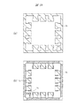
図61に、QFNの他の例であるタブ有りパッケージの裏面の要部平面図を示す。封止体MO4の外周部の裏面には、複数(20個)のリードLE4の裏面がそれぞれ露出している。さらに、封止体MO4の中央部の裏面には、1個の四角形のタブ(アイランド)LE5が露出している。前述の図58と同様に、図61中に示す数字は各リードLE4のインデックスであり、インデックス1に該当するリードLE4を「1pin」と言う。封止体MO4の裏面から露出しているタブLE5の1つの角部に切り欠け部を形成することにより、1pinを認識することができる。
FIG. 61 shows a plan view of the main part of the back surface of a tabbed package as another example of QFN. On the back surface of the outer peripheral portion of the sealing body MO4, the back surfaces of the plural (20) leads LE4 are exposed. Furthermore, one rectangular tab (island) LE5 is exposed on the back surface of the central portion of the sealing body MO4. Similarly to FIG. 58 described above, the numbers shown in FIG. 61 are the indexes of the respective leads LE4, and the lead LE4 corresponding to the
ところで、このようなパッケージ構造を有する半導体装置の特性選別においては、従来トレイ方式の特性選別またはプローバー方式の特性選別を採用していた。 By the way, in the characteristic selection of the semiconductor device having such a package structure, the tray type characteristic selection or the prober type characteristic selection has been conventionally employed.
しかしながら、トレイ方式の特性選別は、個々の半導体装置(半導体パッケージ)をトレイに詰めるため、作業に長時間を要していた。また、プローバー方式の特性選別は、品種切り替えなどに時間がかかるためフレキシビリティが不足していた。さらに、トレイ方式の特性選別およびプローバー方式の特性選別では、検査装置による特性選別の後に、別途半導体装置を梱包する梱包装置が必要であった。 However, the tray-type characteristic selection requires a long time for work because individual semiconductor devices (semiconductor packages) are packed in the tray. In addition, the prober-type characteristic selection is not flexible enough because it takes time to change the product type. Further, in the tray type characteristic selection and the prober type characteristic selection, a packing device for packing the semiconductor device separately is required after the characteristic selection by the inspection apparatus.
そこで、本発明者らは、パーツフィーダー方式の特性選別の採用を検討した。パーツフィーダ方式の特性選別は、トレイ方式の特性選別よりも作業時間が短縮でき、かつ品種切り替えも容易に行えるという利点を有している。さらに、半導体装置の検査および梱包も一台の装置において連続して行うことができる。 Therefore, the present inventors examined the use of part feeder type characteristic selection. Part feeder type characteristic selection has advantages in that the work time can be shortened and the product type can be easily switched over, compared to tray type characteristic selection. Further, the inspection and packing of the semiconductor device can be continuously performed in one device.
ところが、パーツフィーダー方式の特性選別では、ダイシングにより個片化された複数の半導体装置が一旦バラバラになるため、検査時には1pinを認識して、半導体装置の向きを揃える必要がある。なお、トレイ方式の特性選別では、ダイシングにより個片化された複数の半導体装置を、例えばコレットを用いて個々にトレイに詰めるため、1pinの識別は不要であった。また、プローバー方式の特性選別では、ダイシングにより個片化された複数の半導体装置を固定リング(Cリング)に貼り付けたまま検査を行うため、1pinの識別は不要であった。 However, in the part feeder type characteristic selection, since a plurality of semiconductor devices separated by dicing are once separated, it is necessary to recognize 1 pin at the time of inspection and align the directions of the semiconductor devices. In the tray type characteristic selection, since a plurality of semiconductor devices separated by dicing are individually packed in a tray using, for example, a collet, identification of 1 pin is unnecessary. Further, in the prober type characteristic selection, since a plurality of semiconductor devices separated by dicing are inspected while being attached to a fixing ring (C ring), identification of 1 pin is unnecessary.
しかし、前述の図58に示したタブレスパッケージでは、1pinの認識ができない。 However, the tabless package shown in FIG. 58 cannot recognize 1 pin.
また、前述の図59および図60に示したタブレスパッケージでは、1pinの認識は可能ではあるが、配線基板の電極を1pinの形状に合わせる必要があるため、1pinの形状を変更するには顧客の許可が必要となる。さらに、前述の図59および図60に示したタブレスパッケージでは、1pinの形状変更による面積の増減は数%程度であるため、半導体装置のサイズが、例えば1辺が2mm程度と小さくなると画像認識が難しくなり、1pinの正確な認識ができなくなる恐れがあった。 In the tabless package shown in FIG. 59 and FIG. 60 described above, 1 pin can be recognized, but the electrode of the wiring board needs to be matched to the shape of 1 pin. Permission is required. Further, in the tabless package shown in FIG. 59 and FIG. 60 described above, the area increase / decrease due to the shape change of 1 pin is about several percent, so that when the size of the semiconductor device becomes small, for example, about 2 mm, image recognition is performed. This makes it difficult to accurately recognize 1 pin.
また、前述の図61に示したタブ有りパッケージでも、同様に、半導体装置のサイズが、例えば1辺が2mm程度と小さくなると画像認識が難しくなり、1pinの正確な認識ができなくなる恐れがあった。 Similarly, in the above-mentioned package with tabs shown in FIG. 61, if the size of the semiconductor device becomes small, for example, about 2 mm on one side, image recognition becomes difficult and accurate recognition of 1 pin may not be possible. .
本実施の形態では、吊りリードにより保持した識別用目印を形成し、この識別用目印を封止体の裏面から露出させることにより、特に、タブレスパッケージにおいて1pinの位置認識を容易に行うことができる技術を開示する。 In the present embodiment, the identification mark held by the suspension lead is formed, and the identification mark is exposed from the back surface of the sealing body, so that the position of 1 pin can be easily recognized particularly in the tabless package. Disclose technologies that can be used.
(実施の形態)
≪半導体装置≫
本実施の形態1による半導体装置の構造を図1〜図3を用いて説明する。ここでは、12個のリード(外部接続端子、外部端子、端子)を備えるタブレスパッケージを例示する。
(Embodiment)
≪Semiconductor device≫
The structure of the semiconductor device according to the first embodiment will be described with reference to FIGS. Here, a tabless package including 12 leads (external connection terminals, external terminals, terminals) is illustrated.
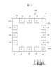
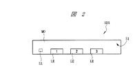
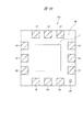
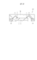
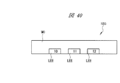
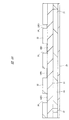
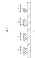
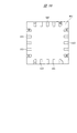
図1は半導体装置の裏面を示す要部平面図、図2は半導体装置の1pin(インデックス1のリード)が配置された外側側面を示す要部側面図、図3は半導体装置の最終番目のインデックスが付されたリード(インデックス12のリード)が配置された外側側面を示す要部側面図である。 1 is a plan view of a main part showing the back surface of the semiconductor device, FIG. 2 is a side view of the main part showing an outer side surface on which 1 pin (lead of index 1) of the semiconductor device is arranged, and FIG. 3 is a final index of the semiconductor device. It is a principal part side view which shows the outer side surface by which the lead | read | reed (lead of the index 12) attached | subjected is arrange | positioned.
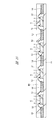
半導体装置(半導体パッケージ)SD1の平面視における形状は四角形であり、表面(上面)、裏面(下面、底面)、および4つの側面(第1側面S1、第2側面S2、第3側面S3、および第4側面S4)を有する。 The shape of the semiconductor device (semiconductor package) SD1 in a plan view is a quadrangle, and includes a front surface (upper surface), a back surface (lower surface, a bottom surface), and four side surfaces (first side surface S1, second side surface S2, third side surface S3, and It has a fourth side S4).
半導体装置SD1は、例えば半導体チップ、半導体チップの周囲に設けられた複数のリード(外部接続端子、外部端子、端子)LE、半導体チップの表面に設けられた複数の電極パッド(ボンディングパッド、表面電極)と複数のリードLEの表面(上面)とをそれぞれ電気的に接続する複数の導電性ワイヤから構成されている。そして、半導体チップ、複数のリードLEの一部(表面(上面)と、側面の一部)、および複数の導電性ワイヤは樹脂封止体(封止体)MOによって封止されている。従って、樹脂封止体MOも平面視における形状は四角形であり、所定の厚さを持って、表面(上面)、表面と反対側の裏面(下面、底面)を有している。 The semiconductor device SD1 includes, for example, a semiconductor chip, a plurality of leads (external connection terminals, external terminals, terminals) LE provided around the semiconductor chip, and a plurality of electrode pads (bonding pads, surface electrodes) provided on the surface of the semiconductor chip. ) And the surface (upper surface) of the plurality of leads LE, respectively. The semiconductor chip, a part of the plurality of leads LE (surface (upper surface) and part of the side surface), and the plurality of conductive wires are sealed with a resin sealing body (sealing body) MO. Accordingly, the resin sealing body MO also has a quadrangular shape in plan view, and has a surface (upper surface) and a back surface (lower surface, bottom surface) opposite to the front surface with a predetermined thickness.
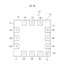
図1に示すように、樹脂封止体MOの裏面には、複数のリードLEの裏面(下面、実装面)が露出する。ここでは12個のリードLEを有する半導体装置SD1を例示しているので、樹脂封止体MOの裏面には12個のリードLEの裏面が露出している。樹脂封止体MOの4つの角部のうち、1つの角部に最も近いリードLEの1個をインデックス1と定め、これを基準にして、連続して樹脂封止体MOの外周部の裏面に配置された複数のリードLEに、順次インデックス(識別番号、通し番号、指標)が付けられている。インデックス1に該当するリードLEを「1pin」と言う。
As shown in FIG. 1, the back surfaces (lower surface, mounting surface) of the plurality of leads LE are exposed on the back surface of the resin sealing body MO. Here, since the semiconductor device SD1 having 12 leads LE is illustrated, the back surface of the 12 leads LE is exposed on the back surface of the resin sealing body MO. Of the four corners of the resin sealing body MO, one of the leads LE closest to one corner is defined as an
半導体装置SD1では、第1側面S1に沿ってインデックス1、2および3のリードLEが配置され、第2側面S2に沿ってインデックス4、5および6のリードLEが配置され、第3側面S3に沿ってインデックス7、8および9のリードLEが配置され、第4側面S4に沿ってインデックス10、11および12のリードLEが配置されている。図1中にリードLEと重ねて付した数字がインデックスである。
In the semiconductor device SD1, the leads LE with
さらに、1pinに最も近い樹脂封止体MOの角部には、1pinに隣接して画像認識エリアPRAが設けられており、この画像認識エリアPRAにおいて、樹脂封止体MOの裏面に識別用目印PPの裏面(下面)が露出している。この識別用目印PPは、後に説明する吊りリードに保持されており、12個のリードLEと同一の導電性部材からなる。上記導電性部材は、例えば銅(Cu)であり、樹脂封止体MOの裏面から露出する12個のリードLEの裏面および識別用目印PPの裏面には、例えばパラジウム(Pd)膜が形成されている。 Further, an image recognition area PRA is provided adjacent to 1 pin at the corner of the resin sealing body MO closest to 1 pin, and an identification mark is provided on the back surface of the resin sealing body MO in the image recognition area PRA. The back surface (lower surface) of PP is exposed. This identification mark PP is held by a suspension lead, which will be described later, and is made of the same conductive member as the twelve leads LE. The conductive member is, for example, copper (Cu), and a palladium (Pd) film, for example, is formed on the back surface of the 12 leads LE exposed from the back surface of the resin sealing body MO and the back surface of the identification mark PP. ing.
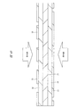
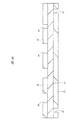
また、図2および図3に示すように、樹脂封止体MOの側面にも、12個のリードLEの側面の他部が露出する。図2および図3中にリードLEと重ねて付した数字がインデックスである。図2に示すように、第1側面S1にはインデックス1、2および3のリードLEの側面の他部が露出し、図3に示すように、第4側面S4にはインデックス10、11および12のリードLEの側面の他部が露出する。また、側面図は省略するが、第1側面S1および第4側面S4と同様に、第2側面S2にはインデックス4、5および6のリードLEの側面の他部が露出し、第3側面S3にはインデックス7、8および9のリードLEの側面の他部が露出する。
Further, as shown in FIGS. 2 and 3, other portions of the side surfaces of the 12 leads LE are also exposed on the side surfaces of the resin sealing body MO. In FIG. 2 and FIG. 3, the number added to the lead LE is an index. As shown in FIG. 2, the other portions of the side surfaces of the leads LE of the
さらに、上記識別用目印PPを保持する吊りリードLLは、1pinが露出する樹脂封止体MOの第1側面S1に露出しており、1pinの傍に1pinと離間して位置する。同様に、上記識別用目印PPを保持する吊りリードLLは、第4側面S4にも露出しており、最終番目のインデックスが付されたリードLE(インデックス12のリードLE)の傍に、このリードLEと離間して位置する。 Further, the suspension lead LL holding the identification mark PP is exposed on the first side surface S1 of the resin sealing body MO where 1 pin is exposed, and is positioned beside 1 pin and separated from 1 pin. Similarly, the suspension lead LL holding the identification mark PP is also exposed on the fourth side surface S4, and this lead is located near the lead LE with the last index (the lead LE of the index 12). Located apart from LE.
識別用目印PPは、画像認識により検知することができる。画像認識では、画像を2値化することにより識別用目印PPの有無を判断する。例えば半導体装置SD1の裏面の複数のリードLEが形成されていない四隅の領域(画像認識エリアPRAおよびこれと同一面積を有する他の三隅の領域)を抜き出して画像認識を行い、ピクセルの違いを判断する。ピクセルの違いが15%以上あれば、反射の有るところ(識別用目印PPの有るところ)と反射の無いところ(識別用目印PPの無いところ)を判断することが可能であるので、画像認識において画像処理する領域(画像認識エリアPRA)に対する識別用目印PPの平面面積は15%以上とすることが好ましい。 The identification mark PP can be detected by image recognition. In the image recognition, the presence / absence of the identification mark PP is determined by binarizing the image. For example, four corner areas (image recognition area PRA and other three corner areas having the same area) on the back surface of the semiconductor device SD1 where the plurality of leads LE are not formed are extracted and image recognition is performed to determine the difference in pixels. To do. If the pixel difference is 15% or more, it is possible to determine where there is reflection (where the identification mark PP is present) and where there is no reflection (where there is no identification mark PP). It is preferable that the planar area of the identification mark PP with respect to the area (image recognition area PRA) for image processing is 15% or more.
このように、1pinの傍に識別用目印PPを設けることにより、1pinの位置識別が容易となる。従って、1pinを認識して半導体装置SD1の向きを揃えることができるので、半導体装置SD1の検査において、パーツフィーダー方式の特性選別を採用することができる。 Thus, by providing the identification mark PP near 1 pin, the position of 1 pin can be easily identified. Therefore, since 1 pin can be recognized and the direction of the semiconductor device SD1 can be aligned, the characteristic selection of the parts feeder method can be employed in the inspection of the semiconductor device SD1.
≪半導体装置の製造方法≫
次に、本実施の形態による半導体装置の製造方法を図4〜図33を用いて工程順に説明する。ここでは、12個のリード(外部接続端子、外部端子、端子)を備えるタブレスパッケージを例示する。
≪Semiconductor device manufacturing method≫
Next, the manufacturing method of the semiconductor device according to the present embodiment will be described in the order of steps with reference to FIGS. Here, a tabless package including 12 leads (external connection terminals, external terminals, terminals) is illustrated.
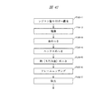
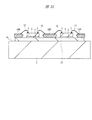
図4〜図7は半導体装置の製造方法を説明する製造工程中における半導体装置の要部断面図である。図8はリードフレームの表面を示す要部平面図、図9はリードフレームの裏面を示す要部平面図である。図10〜図22はリードフレームの製作工程を説明する図である。図23〜図27は半導体装置の製造方法を説明する製造工程中における半導体装置の要部断面図である。図28は半導体装置の表面を示す要部平面図、図29は半導体装置の裏面を示す要部平面図、図30は半導体装置の断面を示す要部断面図である。図31は自動部品供給装置を説明する概略図である。図32はパーツフィーダー方式の特性選別を説明する工程図である。図33は半導体装置の製造方法を説明する工程図である。 4 to 7 are fragmentary cross-sectional views of the semiconductor device during the manufacturing process for explaining the method of manufacturing the semiconductor device. FIG. 8 is a principal plan view showing the front surface of the lead frame, and FIG. 9 is a principal plan view showing the back surface of the lead frame. 10 to 22 are views for explaining a manufacturing process of the lead frame. 23 to 27 are main-portion cross-sectional views of the semiconductor device during the manufacturing process for explaining the method of manufacturing the semiconductor device. FIG. 28 is a main part plan view showing the front surface of the semiconductor device, FIG. 29 is a main part plan view showing the back surface of the semiconductor device, and FIG. 30 is a main part cross sectional view showing a cross section of the semiconductor device. FIG. 31 is a schematic diagram illustrating an automatic component supply apparatus. FIG. 32 is a process diagram for explaining the characteristic selection of the parts feeder system. FIG. 33 is a process diagram illustrating a method for manufacturing a semiconductor device.
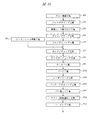
<ウエハ準備工程P1>
図4に示すように半導体ウエハ1を準備する。半導体ウエハ1は単結晶シリコンからなり、その直径は、例えば200mmまたは300mm、その厚さ(第1の厚さ)は、例えば0.7mm以上(製造工程への投入時の値)である。半導体ウエハ1は、第1主面(表面)1x、第1主面1xにマトリックス状に区画形成された複数のチップ領域1CA、複数のチップ領域1CAのうちの互いに隣り合うチップ領域1CA間に形成された切断領域(スクライブ領域、ダイシング領域、ダイシングライン)1SA、および第1主面1xとは反対側の第2主面(裏面)1yを有している。
<Wafer preparation process P1>
As shown in FIG. 4, a
半導体ウエハ1の第1主面1xの各チップ領域1CAには、これに限定されないが、複数の半導体素子と、絶縁層と配線層とをそれぞれ複数段積み重ねた多層配線層と、この多層配線層を覆うようにして形成された表面保護膜とから構成される集積回路が形成されている。上記絶縁層は、例えば酸化シリコン(SiO2)膜で形成されている。上記配線層は、例えばアルミニウム(Al)、タングステン(W)、または銅などの金属膜で形成されている。上記表面保護膜は、例えば酸化シリコン膜または窒化シリコン(Si3N4)膜等の無機絶縁膜および有機絶縁膜を積み重ねた多層膜で形成されている。また、半導体ウエハ1の第1主面1xの各チップ領域1CAには、上記複数の半導体素子と電気的に接続された複数の電極パッド(ボンディングパッド、表面電極)2が各チップ領域1CAの各辺に沿って配置されている(図4には、複数の電極パッド2のうちの一部を記載)。これら複数の電極パッド2は、上記多層配線層のうちの最上層の配線からなり、上記表面保護膜にそれぞれの電極パッド2に対応して形成された開口部により露出している。
Although not limited to this, each chip region 1CA of the first
<バックグラインド工程P2>
半導体ウエハ1の第1主面1x側に集積回路を覆う保護テープ(バックグラインドテープ)を貼り付けた後、半導体ウエハ1の第2主面1yを、研削材(例えば粗さ♯360)を用いて粗研削することにより、半導体ウエハ1の厚さを所定の厚さまで薄くする。続いて半導体ウエハ1の第2主面1yを、先に使用した研削材よりも目の粗さが細かい研削材(例えば粗さ♯1500または♯2000)を用いて仕上げ研削することにより、粗研削時に生じた半導体ウエハ1の第2主面1yの歪みを除去する(バックグラインド)。さらに、仕上げ研削時に生じた半導体ウエハ1の第2主面1yの研磨スジを、例えばスピンエッチ法、CMP(Chemical Mechanical Polishing)法などにより除去する(ストレスリリーフ)。上記バックグラインドおよび上記ストレスリリーフを終えた時点での半導体ウエハ1の厚さ(第2の厚さ)は、例えば0.13mmである。なお、上記ストレスリリーフは全ての半導体ウエハ1に対して行う必要はなく、半導体チップに要求される強度に応じて行う。
<Back grinding process P2>
After a protective tape (back grind tape) covering the integrated circuit is attached to the first
<樹脂シート貼り付け工程P3>
図5に示すように、半導体ウエハ1の第2主面1yに、フィルム状の樹脂シート(接着シート、接着フィルム、封止材)3を貼り付ける。樹脂シート3は、半導体装置SD1として完成した後において、半導体チップの裏面を保護する封止材として機能する。樹脂シート3は、例えば熱硬化型であり、フィラー(SiO2の粒)を含有するエポキシ系樹脂からなる。その厚さは、例えば20〜30μmであり、25μmを中心値とする周辺範囲が好適である。また、そのフィラー含有量は、例えば60wt%である。その後、樹脂シート3が貼り付けられた半導体ウエハ1に対して熱処理を施す。
<Resin sheet pasting process P3>
As shown in FIG. 5, a film-like resin sheet (adhesive sheet, adhesive film, sealing material) 3 is attached to the second main surface 1 y of the
<ダイシングテープ工程P4>
図6に示すように、ダイシングテープ4を準備する。なお、図示はしないが、ダイシングテープ4の周縁部には、平面視において環状のフレームが貼り付けられている。ダイシングテープ4は、例えばポリオリフィンを基材とし、その厚さは、例えば90μmである。また、ダイシングテープ4の上面(半導体ウエハ1が固定される面)には、図示はしないが、接着層が形成されている。接着層は、例えばアクリル系UV硬化型の粘着剤であり、例えばUV照射前は200g/25mm、UV照射後は10〜20g/25mmの粘着力を有している。
<Dicing tape process P4>
As shown in FIG. 6, a dicing
次に、ダイシングテープ4の上面と半導体ウエハ1の第2主面1yとを対向させて、両者を樹脂シート3を介して貼り付ける。これにより、ダイシングテープ4の上面に、樹脂シート3を介して半導体ウエハ1が固定される。
Next, the upper surface of the dicing
<ウエハダイシング工程P5>
図7に示すように、例えばダイヤモンド微粒を貼り付けた極薄の円形刃を用いて、半導体ウエハ1を切断領域1SAに沿って縦、横に切断する。同時に、樹脂シート3も半導体ウエハ1の切断領域1SAに沿って縦、横に切断する。半導体ウエハ1は半導体チップ5に個片化されるが、個片化された後も半導体チップ5はダイシングテープ4を介してフレームに固定されているため、整列した状態を維持している。また、前の製造工程である樹脂シート貼り付け工程P3において、半導体ウエハ1の第2主面1yに樹脂シート3が強く接着されているので、半導体チップ5が樹脂シート3から剥がれて、半導体チップ5の飛散等の問題も生じることはない。
<Wafer dicing process P5>
As shown in FIG. 7, the
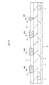
<リードフレーム準備工程P6>
図8および図9に示すように、リードフレームLF1を準備する。リードフレームLF1は、表面(上面)、表面と反対側の裏面(下面)とを有し、例えば銅などの導電性部材からなる。リードフレームLF1は、半導体製品1つ分に該当し、チップ搭載領域を囲む四角形の保持枠(保持部)に12個のリードLEおよび吊りリードLLを有する単位フレームが複数配列した構成となっている。図8および図9には単位フレームに該当するリードフレームLF1の一部を示している。
<Lead frame preparation process P6>
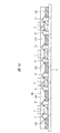
As shown in FIGS. 8 and 9, a lead frame LF1 is prepared. The lead frame LF1 has a front surface (upper surface) and a back surface (lower surface) opposite to the front surface, and is made of a conductive member such as copper. The lead frame LF1 corresponds to one semiconductor product, and has a configuration in which a plurality of unit frames having twelve leads LE and suspension leads LL are arranged on a rectangular holding frame (holding portion) surrounding the chip mounting area. . 8 and 9 show a part of the lead frame LF1 corresponding to the unit frame.
チップ搭載領域を囲む保持枠は、互いに離間して第1方向に延在する2つの第1保持部LH1と第3保持部LH3、互いに離間して第1方向と直交する第2方向に延在する2つの第2保持部LH2と第4保持部LH4により構成される。そして、単位フレームの中央部(チップ搭載領域)を囲むように、12個のリードLEが配置されている。12個のリードLEには、インデックス(識別番号、通し番号、指標)が付けられており、単位フレームの1つの角部を選択し、この角部に最も近いリードLEの1つをインデックス1と定める。そして、これを基準として、連続して単位フレームの周囲に配置されたリードLEに、順次インデックスが付けられている。インデックス1に該当するリードLEが、前述したように「1pin」である。図8および図9中にリードLEと重ねて付した数字がインデックスである。
The holding frame that surrounds the chip mounting area is separated from each other by two first holding portions LH1 and third holding portions LH3 that extend in the first direction, and are separated from each other and extend in the second direction perpendicular to the first direction. The second holding part LH2 and the fourth holding part LH4 are configured. Then, twelve leads LE are arranged so as to surround the center portion (chip mounting region) of the unit frame. Twelve leads LE are indexed (identification number, serial number, index). One corner of the unit frame is selected, and one of the leads LE closest to the corner is defined as
また、これら12個のリードLEは第1保持部LH1、第2保持部LH2、第3保持部LH3、または第4保持部LH4に連結保持されている。例えば、インデックス1、2、および3に該当するリードLEは第1保持部LH1に連結保持され、インデックス4、5、および6に該当するリードLEは第2保持部LH2に連結保持され、インデックス7、8、および9に該当するリードLEは第3保持部LH3に連結保持され、インデックス10、11、および12に該当するリードLEは第4保持部LH4に連結保持されている。
Further, these 12 leads LE are connected and held by the first holding part LH1, the second holding part LH2, the third holding part LH3, or the fourth holding part LH4. For example, the leads LE corresponding to the
さらに、吊りリードLLは、第1方向に沿って延在する第1部分と、第2方向に沿って延在する第2部分とから構成される。吊りリードLLの第2部分の一端は第1保持部LH1と第4保持部LH4とが交差する角部とインデックス1のリードLE(1pin)との間の第1保持部LH1に連結し、吊りリードLLの第1部分の一端は上記角部とインデックス12のリードLE(最終番目のインデックスが付されたリードLE)との間の第4保持部LH4とに連結する。そして、吊りリードLLの第1部分の他端と吊りリードLLの第2部分の他端とが識別用目印PPを保持している。
Furthermore, the suspension lead LL includes a first portion extending along the first direction and a second portion extending along the second direction. One end of the second portion of the suspension lead LL is connected to the first retention portion LH1 between the corner where the first retention portion LH1 and the fourth retention portion LH4 intersect and the lead LE (1 pin) of the
リードフレームLF1の表面は平坦であるが、リードフレームLF1の裏面の一部には、リードフレームLF1を厚さを約半分の厚さに加工するハーフエッチングが施されており(例えば図9に示すハッチングを付した部分)、リードフレームLF1の裏面は平坦ではない。リードフレームLF1のハーフエッチングが施されていない部分の厚さは、例えば0.125mmである。 Although the surface of the lead frame LF1 is flat, a part of the back surface of the lead frame LF1 is subjected to half etching for processing the lead frame LF1 to a half thickness (for example, as shown in FIG. 9). The hatched portion) and the back surface of the lead frame LF1 are not flat. The thickness of the portion of the lead frame LF1 that is not half-etched is, for example, 0.125 mm.
12個のリードLEにおいては、後のモールド工程において、樹脂封止体の裏面から露出するリードLEの一部を除いて、リードLEの裏面側からハーフエッチングが施されている。ハーフエッチングが施されたリードLEの他部は、後のモールド工程において、樹脂封止体により封止される。その厚さは、例えば0.065mmである。 The twelve leads LE are half-etched from the back side of the lead LE except for a part of the lead LE exposed from the back side of the resin-encapsulated body in a later molding step. The other part of the lead LE subjected to the half etching is sealed with a resin sealing body in a later molding step. The thickness is, for example, 0.065 mm.
また、第1保持部LH1と第4保持部LH4とに繋がる吊りリードLLでは、吊りリードLLの裏面側からハーフエッチングが施されている。この吊りリードLLに保持され、ハーフエッチングが施されていない導電性部材が、後のモールド工程において、その裏面が樹脂封止体の裏面から露出する識別用目印PPとなる。ハーフエッチングが施された吊りリードLLは、後のモールド工程において、樹脂封止体により封止される。その厚さは、例えば0.065mmである。 Further, in the suspension lead LL connected to the first holding unit LH1 and the fourth holding unit LH4, half etching is performed from the back side of the suspension lead LL. The conductive member which is held by the suspension lead LL and which has not been half-etched becomes an identification mark PP whose back surface is exposed from the back surface of the resin sealing body in a later molding step. The suspension lead LL subjected to the half etching is sealed with a resin sealing body in a later molding step. The thickness is, for example, 0.065 mm.
また、保持部においては、第1保持部LH1と第2保持部LH2とが交差する角部、第2保持部LH2と第3保持部LH3とが交差する角部、第3保持部LH3と第4保持部LH4とが交差する角部、第4保持部LH4と第1保持部LH1とが交差する角部を除いて、第1保持部LH1、第2保持部LH2、第3保持部LH3、および第4保持部LH4には、これらの裏面側からハーフエッチングが施されている。ハーフエッチングが施された第1保持部LH1、第2保持部LH2、第3保持部LH3、および第4保持部LH4の厚さは、例えば0.065mmである。 Further, in the holding portion, the corner portion where the first holding portion LH1 and the second holding portion LH2 intersect, the corner portion where the second holding portion LH2 and the third holding portion LH3 intersect, the third holding portion LH3 and the first holding portion. Except for the corner where the four holding portions LH4 intersect and the corner where the fourth holding portion LH4 and the first holding portion LH1 intersect, the first holding portion LH1, the second holding portion LH2, the third holding portion LH3, The fourth holding portion LH4 is half-etched from the back side. The thicknesses of the first holding part LH1, the second holding part LH2, the third holding part LH3, and the fourth holding part LH4 subjected to the half etching are, for example, 0.065 mm.
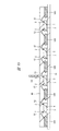
次に、リードフレームLF1の製作工程について図10〜図22を用いて説明する。図10はリードフレームLF1の製作方法を説明する工程図である。図11(a)、図13(a)、図15(a)、図17(a)、図19(a)、および図21(a)はリードフレームLF1の表面を示す要部平面図、図11(b)、図13(b)、図15(b)、図17(b)、図19(b)、および図21(b)はリードフレームLF1の裏面を示す要部平面図である。図12、図14、図16、図18、図20、および図22はリードフレームLF1の断面を示す要部断面図である。 Next, the manufacturing process of the lead frame LF1 will be described with reference to FIGS. FIG. 10 is a process diagram illustrating a method of manufacturing the lead frame LF1. 11 (a), FIG. 13 (a), FIG. 15 (a), FIG. 17 (a), FIG. 19 (a), and FIG. 21 (a) are plan views and main parts showing the surface of the lead frame LF1. 11 (b), FIG. 13 (b), FIG. 15 (b), FIG. 17 (b), FIG. 19 (b), and FIG. 21 (b) are main part plan views showing the back surface of the lead frame LF1. 12, FIG. 14, FIG. 16, FIG. 18, FIG. 20, and FIG. 22 are cross-sectional views of main parts showing the cross section of the lead frame LF1.
・P6−(1)銅生材準備工程
図11および図12に示すように、導電性部材、例えば銅生材6を準備する。銅生材6は、表面(上面)6xと、表面6xと反対側の裏面(下面)6yとを有し、その厚さは、例えば0.125mmである。
-P6- (1) Copper raw material preparation process As shown in FIG. 11 and FIG. 12, a conductive member, for example, the copper
・P6−(2)レジスト塗布工程
図13および図14に示すように、銅生材6の表面6xおよび裏面6yにそれぞれレジスト膜7を塗布する。
P6- (2) Resist Application Step As shown in FIGS. 13 and 14, a resist
・P6−(3)露光工程
図15および図16に示すように、レジスト膜7を残す領域(リードフレームが形成される領域)に銅生材6の表面6x側および裏面6y側からそれぞれ露光(UV(Ultra Violet)光)を照射して、レジスト膜7を硬化させる。図16中、レジスト膜7の硬化部分を符号7Aで示す。
P6- (3) Exposure Step As shown in FIG. 15 and FIG. 16, exposure is performed from the
・P6−(4)現像工程
図17および図18に示すように、レジスト膜7,7Aに現像処理を施して、硬化したレジスト膜7Aを銅生材6の表面6xおよび裏面6yに残す。銅生材6の表面6xに形成されたレジスト膜7Aの形状と、銅生材6の裏面6yに形成されたレジスト膜7Aの形状とは互いに異なっている。その異なる領域がハーフエッチングが施される領域となる。
P6- (4) Development Step As shown in FIGS. 17 and 18, the resist
すなわち、銅生材6の表面6x側から透視したときに、銅生材6の表面6xに形成されたレジスト膜7Aが覆う領域は、銅生材6の裏面6yに形成されたレジスト膜7Aが覆う領域よりも広いが、銅生材6の裏面6yに形成されたレジスト膜7Aが覆う領域は全て銅生材6の表面6xに形成されたレジスト膜7Aが覆う領域と重なる。
That is, the region covered by the resist
・P6−(5)エッチング工程
図19および図20に示すように、銅生材6の表面6x側および裏面6y側からそれぞれ溶解液8を銅生材6にスプレーして、レジスト膜7Aに覆われていない銅生材6をエッチングする。表面6xおよび裏面6yともにレジスト膜7Aが形成されていない領域の銅生材6は厚さ方向に全てエッチングされる。一方、表面6xにはレジスト膜7Aは形成されているが裏面6yにはレジスト膜7Aが形成されていない領域の銅生材6は、裏面6yから厚さ方向に約半分がエッチング(ハーフエッチング)される。
P6- (5) Etching Step As shown in FIGS. 19 and 20, the
すなわち、銅生材6の表面6x側から透視したときに、銅生材6の表面6xに形成されたレジスト膜7Aと銅生材6の裏面6yに形成されたレジスト膜7Aとが重なっている領域では、銅生材6はエッチングされない。しかし、銅生材6の表面6x側から透視したときに、銅生材6の表面6xにレジスト膜7Aは形成されているが、銅生材6の裏面6yにレジスト膜7Aは形成されていない領域では、銅生材6は表面6x側に一部を残して、裏面6y側から厚さ方向にエッチングされる。
That is, when seen through from the
従って、識別用目印PPが形成される領域では、銅生材6の表面6x側から透視したときに、銅生材6の表面6xに形成されたレジスト膜7Aと銅生材6の裏面6yに形成されたレジスト膜7Aとが重なっており、銅生材6はエッチングされない。しかし、吊りリードLLが形成される領域では、銅生材6の表面6x側から透視したときに、銅生材6の表面6xにレジスト膜7Aは形成されているが、銅生材6の裏面6yにレジスト膜7Aは形成されておらず、銅生材6は表面6x側に一部を残して、裏面6y側から厚さ方向にエッチングされる。
Therefore, in the region where the identification mark PP is formed, the resist
・P6−(6)剥離工程
図21および図22に示すように、レジスト膜7Aを除去することにより、リードフレームLF1が完成する。
P6- (6) Stripping Step As shown in FIGS. 21 and 22, the lead frame LF1 is completed by removing the resist
なお、本実施の形態では、平面視における識別用目印PPの形状を円形としたが、これに限定されるものではなく、例えば四角形であってもよい。 In the present embodiment, the shape of the identification mark PP in plan view is circular, but the shape is not limited to this, and may be, for example, a quadrangle.
次に、リードフレームLF1にめっき処理を施して、リードフレームLF1の表面および裏面に、例えばパラジウム膜(図示は省略)をめっき法により形成する。 Next, a plating process is performed on the lead frame LF1, and, for example, a palladium film (not shown) is formed on the front and back surfaces of the lead frame LF1 by a plating method.
<ダイボンディング工程P7>
ダイシングテープ4の下面側から紫外線を照射して、ダイシングテープ4の上面に形成された接着層の接着力を、例えば10〜20g/25mm程度に低下させることにより、接着層を硬化させる。これにより、各半導体チップ5がダイシングテープ4から剥がれやすくなる。
<Die bonding process P7>
The adhesive layer is cured by irradiating ultraviolet rays from the lower surface side of the dicing
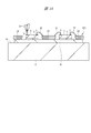
次に、図23に示すように、リードフレームLF1の裏面と、熱源を有するヒートステージ9の表面(上面)9xとを対向させて、ヒートステージ9の表面9x上にフレームテープ10を介してリードフレームLF1を配置する。ヒートステージ9は、例えばステンレス(SUS430)などの導電性部材から成り、例えば40〜80℃に加熱されている。
Next, as shown in FIG. 23, the back surface of the lead frame LF1 and the surface (upper surface) 9x of the
次に、半導体チップ5の表面を円筒コレット11によって吸着し、保持した後、半導体チップ5をダイシングテープ4から引き剥がしてピックアップする。ダイシングテープ4の上面に形成された接着層の接着力が弱められているので、薄く強度が低下している半導体チップ5であっても確実にピックアップすることができる。半導体チップ5の裏面には、樹脂シート3が接着している。
Next, after the surface of the
次に、ピックアップされた半導体チップ5は、フレームテープ10の所定のチップ搭載領域に搬送される。続いて、半導体チップ5の裏面に接着している樹脂シート3を介して、フレームテープ10のチップ搭載領域に半導体チップ5を配置し、熱(例えば40〜80℃)を加えることで、フレームテープ10のチップ搭載領域に半導体チップ5を固定する。
Next, the picked-up
<ワイヤボンディング工程P8>
図24に示すように、半導体チップ5の表面の縁辺に配置された複数の電極パッド2と、チップ搭載領域の周囲に位置する複数のリードLEの表面とを、例えば熱圧着に超音波振動を併用したネイルヘッドボンディング法(ボールボンディング法)により、複数の導電性ワイヤ12を用いてそれぞれ電気的に接続する。具体的には、導電性ワイヤ12の先端をアーク放電により溶融して表面張力でボールを形成し、それをキャピラリ(円筒状の接続治具)13により電極パッド2およびリードLEの表面に、例えば120kHzの超音波振動を加えながら熱圧着する。
<Wire bonding process P8>
As shown in FIG. 24, ultrasonic vibration is applied to, for example, thermocompression bonding between the plurality of
また、主として、正ボンディング方式(半導体チップ5の電極パッド2と導電性ワイヤ12の一部を接続した後に、リードLEと導電性ワイヤ12の他部を接続する方式)を用いるが、逆ボンディング方式(リードLEと導電性ワイヤ12の一部を接続した後に、半導体チップ5の電極パッド2と導電性ワイヤ12の他部を接続する方式)を用いても良い。
In addition, a normal bonding method (a method in which the
<モールド工程P9>
図25に示すように、複数の半導体チップ5が搭載されたリードフレームLF1およびフレームテープ10を金型成型機にセットし、温度を上げて液状化した封止樹脂を金型成型機に圧送して流し込み、フレームテープ10の半導体チップ等が搭載された面側を封止樹脂で封入して、1つの樹脂封止体(封止体)MOを形成する。樹脂封止体MOは、低応力化を図ることを目的として、例えばフェノール系硬化剤、シリコーンゴム、および多数のフィラー(例えばシリカ)などが添加されたエポキシ系の熱硬化性絶縁樹脂からなる。
<Mold process P9>
As shown in FIG. 25, the lead frame LF1 and the
<ベーク工程P10>
例えば175℃の温度で5時間の熱処理(ポストキュアベーク)を施す。この熱処理は、例えばエア(Air)ベークである。これにより、複数の半導体チップ5、複数のリードLEのそれぞれの一部(表面と、側面の一部)、複数の導電性ワイヤ12、および識別用目印PPの一部(表面(上面)と、側面)などが樹脂封止体MOによって封止される。樹脂封止体MOの厚さは、例えば300μmである。
<Bake process P10>
For example, a heat treatment (post cure bake) is performed at a temperature of 175 ° C. for 5 hours. This heat treatment is, for example, air baking. Accordingly, a plurality of
<レーザーマーク工程P11>
図26に示すように、フレームテープ10を除去した後、レーザー14を用いて樹脂封止体MOの上面に品名などを捺印する。
<Laser mark process P11>
As shown in FIG. 26, after the
<パッケージダイシング工程P13>
図27に示すように、ダイシングテープ15を準備する。続いて、ダイシングテープ15の上面に、複数の半導体チップ5、複数のリードLEのそれぞれの一部(表面と、側面の一部)、および複数の導電性ワイヤ12などを被覆した樹脂封止体MOを固定する。
<Package dicing process P13>
As shown in FIG. 27, a dicing
次に、例えばダイヤモンド微粒を貼り付けた極薄の円形刃を用いて、樹脂封止体MOの裏面側から樹脂封止体MO、複数のリードLE、および吊りリードLLをスクライブ領域に沿って縦、横に切断する。樹脂封止体MOは半導体装置(半導体パッケージ)SD1に個片化されるが、個片化された後も半導体装置SD1はダイシングテープ15を介して固定されているため、整列した状態を維持している。続いて、樹脂封止体MOを切断する際に発生した屑などを除去するために、半導体装置SD1を洗浄する。
Next, the resin sealing body MO, the plurality of leads LE, and the suspension leads LL are vertically extended along the scribe region from the back surface side of the resin sealing body MO using, for example, an extremely thin circular blade with diamond fine particles attached thereto. Cut sideways. Although the resin sealing body MO is separated into individual semiconductor devices (semiconductor packages) SD1, the semiconductor device SD1 is fixed through the dicing
<バラ落とし工程P14>
図28〜図30に示すように、ダイシングテープ15を除去することにより、個々の半導体装置SD1に分ける。図28に示すように、半導体装置SD1の表面には、レーザマークが印字されている。また、図29に示すように、半導体装置SD1の裏面には、12個のリードLEのそれぞれの裏面、および半導体チップ5の裏面に貼られた樹脂シート3が露出している。従って、半導体チップ5の裏面は、樹脂シート3に保護されている。また、半導体装置SD1の側面には、12個のリードの側面の一部が樹脂封止体MOから露出している。なお、樹脂シート3は樹脂封止体MOと区別して視認することが難しいため、後述する1pinの位置認識では樹脂シート3は認識されない。
<Rose drop process P14>
As shown in FIGS. 28 to 30, the dicing
個々に分けられた複数の半導体装置SD1は、後の工程において検査され、良品と判断された半導体装置SD1のみが梱包される。本実施の形態では、図31に示す自動部品供給装置AFを用いて検査および梱包を行う。従って、複数の半導体装置SD1は、自動部品供給装置AFのパーツフィーダー部AFPにバラバラの状態で投入される。パーツフィーダー部AFPに投入された複数の半導体装置SD1は、自動部品供給装置AFにおいて、順次検査され(テスト(特性選別)工程P15)、良品と判断された半導体装置SD1は梱包される(テーピング工程P16)。 A plurality of individually divided semiconductor devices SD1 are inspected in a later process, and only the semiconductor devices SD1 determined to be non-defective are packed. In the present embodiment, inspection and packing are performed using the automatic component feeder AF shown in FIG. Accordingly, the plurality of semiconductor devices SD1 are thrown into the parts feeder portion AFP of the automatic component feeder AF in a disjoint state. The plurality of semiconductor devices SD1 inserted into the parts feeder unit AFP are sequentially inspected (test (characteristic selection) step P15) by the automatic component supply device AF, and the semiconductor devices SD1 determined to be non-defective products are packed (taping step). P16).
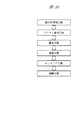
<テスト(特性選別)工程P15>
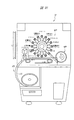
図32に示すパーツフィーダー方式の特性選別の工程に従って、半導体装置SD1を自動部品供給装置AFのパーツフィーダー部AFPから検査部AFTに搬送し、製品規格に沿って選別する。自動部品供給装置AFのパーツフィーダー部AFPにバラバラに投入した複数の半導体装置SD1を一個ずつ自動部品供給装置AFの検査部AFTへ搬送する。
<Test (characteristic selection) process P15>
According to the part feeder type characteristic selection process shown in FIG. 32, the semiconductor device SD1 is transported from the parts feeder part AFP of the automatic component supply apparatus AF to the inspection part AFT, and is selected according to the product standard. A plurality of semiconductor devices SD1 that are separately loaded into the parts feeder unit AFP of the automatic component feeder AF are conveyed one by one to the inspection unit AFT of the automatic component feeder AF.
検査部AFTでは、まず、半導体装置SD1の形状および面積を判別して、樹脂封止体MOから露出している12個のリードLEおよび識別用目印PPを認識し、識別用目印PPから1pinの位置認識を行う。続いて、1pinの位置を基に半導体装置SD1を90°、180°、または−90°回転させて、整列させる。続いて、半導体装置SD1のテスト(特性選別)を行う。テストにおいて不良と判断された半導体装置SD1は取り除かれる。 The inspection unit AFT first determines the shape and area of the semiconductor device SD1, recognizes the 12 leads LE and the identification mark PP exposed from the resin sealing body MO, and identifies 1 pin from the identification mark PP. Perform position recognition. Subsequently, the semiconductor device SD1 is rotated by 90 °, 180 °, or −90 ° based on the position of 1 pin and aligned. Subsequently, a test (characteristic selection) of the semiconductor device SD1 is performed. The semiconductor device SD1 determined to be defective in the test is removed.
<テーピング工程P16>
テストにおいて良と判断された半導体装置SD1を自動部品供給装置AFのテーピング部AFCにおいて、キャリアテープCTに収納する。その後、キャリアテープCTに収納された半導体装置SD1の外観、例えばレーザマークおよび傷の有無等が検査される。その後、例えばキャリアテープCTをリールに巻き取り、防湿された袋にリールを収納し、この状態で出荷する。
<Taping process P16>
The semiconductor device SD1 determined to be good in the test is stored in the carrier tape CT in the taping unit AFC of the automatic component supply device AF. Thereafter, the appearance of the semiconductor device SD1 accommodated in the carrier tape CT, for example, the presence or absence of a laser mark and a flaw is inspected. Thereafter, for example, the carrier tape CT is wound around the reel, and the reel is stored in a moisture-proof bag, and shipped in this state.
このように、本実施の形態1によれば、識別用目印PPにより1pinの位置を容易に認識できることから、タブレスパッケージであってもパーツフィーダ方式の特性選別を採用することができる。 As described above, according to the first embodiment, the position of 1 pin can be easily recognized by the identification mark PP. Therefore, even in the case of a tabless package, it is possible to employ part feeder type characteristic selection.
(実施の形態の第1変形例)
前述した実施の形態では、例えば前述の図8および図9に示したように、識別用目印PPは、第1方向に延在する第1保持部LH1と第2方向に延在する第4保持部LH4とが交差する角部とインデックス1のリードLE(1pin)との間の第1保持部LH1に連結し、上記角部とインデックス12のリードLEとの間の第4保持部LH4に連結した吊りリードLLに保持されている。しかし、第1方向に延在する第1保持部LH1または第2方向に延在する第4保持部LH4のどちらか一方に連結する吊りリードによって識別用目印PPを保持しても良い。
(First Modification of Embodiment)
In the embodiment described above, for example, as shown in FIG. 8 and FIG. 9 described above, the identification mark PP has the first holding portion LH1 extending in the first direction and the fourth holding extending in the second direction. Connected to the first holding part LH1 between the corner where the part LH4 intersects and the lead LE (1 pin) of the
リードフレームの第1変形例を図34および図35を用いて説明する。図34はリードフレームの表面を示す要部平面図、図35はリードフレームの裏面を示す要部平面図である。 A first modification of the lead frame will be described with reference to FIGS. 34 and 35. FIG. FIG. 34 is a principal plan view showing the front surface of the lead frame, and FIG. 35 is a principal plan view showing the back surface of the lead frame.
図34および図35に示すように、リードフレームLF2は、前述の図8および図9に示したリードフレームLF1と同様に、第1保持部LH1、第2保持部LH2、第3保持部LH3、および第4保持部LH4を有し、単位フレームの中央部(チップ搭載領域)を囲むように、12個のリードLEが配置されている。また、12個のリードLEには、インデックス(識別番号、通し番号、指標)が付けられており、インデックス1に該当するリードLEが1pinである。また、1pinの傍に1pinと離間して、後のモールド工程において、その裏面が樹脂封止体の裏面から露出する識別用目印PPが形成されている。図34中に、リードLEと重ねて付した数字がインデックスである。
As shown in FIGS. 34 and 35, the lead frame LF2 is similar to the lead frame LF1 shown in FIGS. 8 and 9, and the first holding part LH1, the second holding part LH2, the third holding part LH3, The twelve leads LE are arranged so as to surround the center portion (chip mounting region) of the unit frame. The 12 leads LE are indexed (identification number, serial number, index), and the lead LE corresponding to the
しかし、このリードフレームLF2では、識別用目印PPは、第1保持部LH1と第4保持部LH4とが交差する角部とインデックス1のリードLE(1pin)との間の第1保持部LH1のみに繋がる吊りリードLLに保持されている。すなわち、吊りリードLLの一端が第1保持部LH1に連結し、吊りリードLLの他端が識別用目印PPを保持している。
However, in this lead frame LF2, the identification mark PP is only the first holding portion LH1 between the corner where the first holding portion LH1 and the fourth holding portion LH4 intersect and the lead LE (1 pin) of the
(実施の形態の第2変形例)
前述した実施の形態では、例えば前述の図30に示したように、1個の半導体チップを樹脂封止する構成の半導体装置SD1を例示したが、2個または3個の半導体チップを樹脂封止する構成の半導体装置にも、本実施の形態は適用することができる。
(Second Modification of Embodiment)
In the embodiment described above, for example, as illustrated in FIG. 30 described above, the semiconductor device SD1 having a configuration in which one semiconductor chip is resin-sealed is illustrated, but two or three semiconductor chips are resin-sealed. The present embodiment can also be applied to a semiconductor device configured as described above.
半導体装置の第2変形例の構造を図36および図37を用いて説明する。図36は半導体装置の断面を示す要部断面図、図37は半導体装置の裏面を示す要部平面図である。 A structure of a second modification of the semiconductor device will be described with reference to FIGS. 36 is a cross-sectional view of a main part showing a cross section of the semiconductor device, and FIG. 37 is a plan view of the main part showing the back surface of the semiconductor device.
図36に示すように、半導体装置(半導体パッケージ)SD2は、2個の半導体チップ5A,5B、半導体チップ5A,5Bのそれぞの裏面に形成された樹脂シート(接着接着シート、接着フィルム、封止材)3A,3B、半導体チップ5A,5Bの周囲に設けられた複数のリードLE、および半導体チップ5A,5Bのそれぞれの表面に配置された複数の電極パッド(ボンディングパッド)と複数のリードLEとを電気的に接続する複数の導電性ワイヤ12から構成されている。半導体チップ5A,5B、樹脂シート3A,3Bの側面、複数のリードLEのそれぞれの一部(表面(上面)と、側面の一部)、および複数の導電性ワイヤ12は樹脂封止体(封止体)MOによって封止されている。
As shown in FIG. 36, the semiconductor device (semiconductor package) SD2 includes two
また、図37に示すように、樹脂封止体MOの下面からは半導体チップ5A,5Bのそれぞれの裏面は露出しておらず、半導体チップ5A,5Bのそれぞれの裏面に接着された樹脂シート3A,3B、複数のリードLEのそれぞれの他部(裏面(下面、実装面))、および識別用目印PPの裏面が露出した構造となっている。なお、樹脂シート3は樹脂封止体MOと区別して視認することが難しいため、1pinの位置認識では樹脂シート3は認識されない。
As shown in FIG. 37, the back surfaces of the
(実施の形態の第3変形例)
前述した実施の形態では、半導体装置のリード(外部接続端子、外部端子、端子)をリードフレームにより形成したが、電解めっき法により形成したリードを用いても良い。
(Third Modification of Embodiment)
In the embodiment described above, the lead (external connection terminal, external terminal, terminal) of the semiconductor device is formed by the lead frame. However, a lead formed by electrolytic plating may be used.
≪半導体装置≫
半導体装置の第3変形例の構造を図38〜図40を用いて説明する。ここでは、12個の電解めっき法により形成したリード(外部接続端子、外部端子、端子)を備えるタブレスパッケージを例示する。
≪Semiconductor device≫
The structure of the third modification of the semiconductor device will be described with reference to FIGS. Here, a tabless package including 12 leads (external connection terminals, external terminals, terminals) formed by electrolytic plating is illustrated.
図38は半導体装置の裏面を示す要部平面図、図39は半導体装置の1pin(インデックス1のリード)が配置された外側側面を示す要部側面図、図40は半導体装置の最終番目のインデックスが付されたリード(インデックス12のリード)が配置された外側側面を示す要部側面図である。 38 is a plan view of the main part showing the back surface of the semiconductor device, FIG. 39 is a side view of the main part showing the outer side surface where 1 pin (lead of index 1) of the semiconductor device is arranged, and FIG. 40 is the last index of the semiconductor device. It is a principal part side view which shows the outer side surface by which the lead | read | reed (lead of the index 12) attached | subjected is arrange | positioned.
図38に示すように、前述の図1に示した半導体装置(半導体パッケージ)SD1と同様に、電解めっき法により形成したリードLEEを用いた半導体装置(半導体パッケージ)SD3も、その裏面(下面、底面)には、複数のリードLEEの裏面(下面、実装面)が露出する。ここでは12個のリードLEEを有する半導体装置SD3を例示しているので、樹脂封止体MOの裏面には12個のリードLEEの裏面が露出している。 As shown in FIG. 38, similarly to the semiconductor device (semiconductor package) SD1 shown in FIG. 1, the semiconductor device (semiconductor package) SD3 using the lead LEE formed by the electrolytic plating method also has a back surface (lower surface, On the bottom surface, the back surfaces (lower surface, mounting surface) of the plurality of leads LEE are exposed. Here, since the semiconductor device SD3 having 12 leads LEE is illustrated, the back surface of the 12 leads LEE is exposed on the back surface of the resin sealing body MO.
そして、1pinに最も近い樹脂封止体MOの角部には、1pinに隣接して画像認識エリアPRAが設けられており、この画像認識エリアPRAにおいて、樹脂封止体MOの裏面に識別用目印PPの裏面が露出している。この識別用目印PPは、複数のリードLEEと同じ製造工程において形成され、12個のリードLEEと同一の導電性部材からなる。なお、図39および図40に示すように、樹脂封止体MOの側面には、12個のリードLEEの側面の一部のみが露出する。 An image recognition area PRA is provided adjacent to 1 pin at the corner of the resin sealing body MO closest to 1 pin. In this image recognition area PRA, an identification mark is provided on the back surface of the resin sealing body MO. The back side of PP is exposed. This identification mark PP is formed in the same manufacturing process as the plurality of leads LEE and is made of the same conductive member as the twelve leads LEE. As shown in FIGS. 39 and 40, only a part of the side surfaces of the 12 leads LEE is exposed on the side surface of the resin sealing body MO.
このように、電解めっき法により形成したリードを採用した半導体装置SD3においても、1pinの傍に識別用目印PPを設けることができる。これにより、1pinを認識して半導体装置SD3の向きを揃えることができるので、半導体装置SD3の検査において、パーツフィーダー方式の特性選別を採用することができる。 Thus, also in the semiconductor device SD3 employing the lead formed by the electrolytic plating method, the identification mark PP can be provided near 1 pin. Thereby, since 1 pin can be recognized and the direction of the semiconductor device SD3 can be aligned, the characteristic selection of the parts feeder system can be employed in the inspection of the semiconductor device SD3.
≪半導体装置の製造方法≫
次に、半導体装置の第3変形例の製造方法を図41〜図57を用いて工程順に説明する。ここでは、電解めっき法により形成した12個のリード(外部接続端子、外部端子、端子)を備えるタブレスパッケージを例示する。
≪Semiconductor device manufacturing method≫
Next, the manufacturing method of the 3rd modification of a semiconductor device is demonstrated in order of a process using FIGS. Here, a tabless package including 12 leads (external connection terminals, external terminals, terminals) formed by electrolytic plating is illustrated.
図41は1個のリードを拡大して示すリードの要部断面図である。図42は複数のリードを有する基材の製造方法を説明する工程図、図43〜図49は複数のリードを有する基材の製造方法を説明する製造工程中における基材の要部断面図、図50〜図54は半導体装置の製造方法を説明する製造工程中における半導体装置の要部断面図である。図55は半導体装置の裏面を示す要部平面図、図56は半導体装置の断面を示す要部断面図である。図57は半導体装置の製造方法を説明する工程図である。 FIG. 41 is a cross-sectional view of a main part of a lead showing an enlarged view of one lead. 42 is a process diagram illustrating a method for manufacturing a substrate having a plurality of leads, and FIGS. 43 to 49 are cross-sectional views of main parts of the substrate during a manufacturing process illustrating a method for manufacturing a substrate having a plurality of leads. 50 to 54 are fragmentary cross-sectional views of the semiconductor device during the manufacturing process for explaining the method of manufacturing the semiconductor device. FIG. 55 is a main part plan view showing the back surface of the semiconductor device, and FIG. 56 is a main part sectional view showing a cross section of the semiconductor device. FIG. 57 is a process diagram illustrating a method for manufacturing a semiconductor device.
ここでは、12個の電解めっき法により形成したリードを備える半導体装置の製造方法について説明するが、これに限定されるものではなく、例えば20個または24個のリードを有する半導体装置の製造方法にも適用することができる。 Here, a method for manufacturing a semiconductor device having 12 leads formed by electrolytic plating will be described. However, the present invention is not limited to this. For example, a method for manufacturing a semiconductor device having 20 or 24 leads is used. Can also be applied.
<ウエハ準備工程P101>から<ウエハダイシング工程P105>までは、前述した半導体装置SD1の製造方法の<ウエハ準備工程P1>から<ウエハダイシング工程P5>と同様であるので、ここでの説明は省略する。従って、<基板準備工程P106>以降の工程について、以下に説明する。 <Wafer preparation step P101> to <Wafer dicing step P105> are the same as <Wafer preparation step P1> to <Wafer dicing step P5> of the method for manufacturing the semiconductor device SD1 described above, and thus description thereof is omitted here. To do. Therefore, the steps after <Substrate Preparation Step P106> will be described below.
<基材準備工程P106>
まず、リードLEEおよび識別用目印PPの形状について説明する。
<Base Material Preparation Step P106>
First, the shapes of the lead LEE and the identification mark PP will be described.
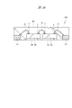
図41に示すように、リードLEEおよび識別用目印PPは、例えば電解めっき法により金(Au)膜LEE1、ニッケル(Ni)膜LEE2、および銀(Ag)膜LEE3(または金膜)を下から順次形成した積層膜により構成され、ニッケル膜LEE2がひさし状に張り出した迫り出し部を有するマッシュルーム形状を有している。リードLEEおよび識別用目印PPの表面(上面)は、母基板21の上面よりも高い位置にあるが、電解めっき法により形成するリードLEEおよび識別用目印PPは、導電性基板(金属板)をパターニングすることで形成されたリードフレームの一部からなるリードの厚さの約半分以下の厚さで形成することができる。また、リードLEEおよび識別用目印PPの形状をマッシュルーム形状とすることにより、後の製造工程であるモールド工程(P110)において、リードLEEおよび識別用目印PPのアンカー効果が期待できる。リードLEEおよび識別用目印PPを構成する金膜LEE1の厚さは、例えば0.03μm、ニッケル膜LEE2Bの厚さは、例えば60μm、銀膜LEE3(または金膜)の厚さは、例えば3μmである。
As shown in FIG. 41, the lead LEE and the identification mark PP are formed by, for example, depositing a gold (Au) film LEE1, a nickel (Ni) film LEE2, and a silver (Ag) film LEE3 (or gold film) from below by electrolytic plating. It has a mushroom shape that is composed of sequentially formed laminated films and has a protruding portion in which the nickel film LEE2 projects in an eave shape. The surface (upper surface) of the lead LEE and the identification mark PP is higher than the upper surface of the
次に、図42〜図49を用いて複数のリードLEEが形成された基材の製造方法について説明する。図42は複数のリードを有する基材の製造方法を説明する工程図、図43〜図49は複数のリードを有する基材の製造方法を説明する製造工程中における基材の要部断面図である。 Next, a method for manufacturing a base material on which a plurality of leads LEE are formed will be described with reference to FIGS. FIG. 42 is a process diagram illustrating a method for manufacturing a base material having a plurality of leads, and FIGS. 43 to 49 are cross-sectional views of main parts of the base material during a manufacturing process illustrating a method for manufacturing a base material having a plurality of leads. is there.
(P106−1:レジスト貼り付け工程〜露光工程)
図43に示すように、母基板21の上面(表面)にレジスト膜22を塗布した後、このレジスト膜22に、所定のパターンが形成されたフィルムマスク23を介して紫外線を露光する。同様に、母基板21の上面と反対側の下面(裏面)にレジスト膜24を塗布した後、このレジスト膜24に、所定のパターンが形成されたフィルムマスク25を介して紫外線を露光する。
(P106-1: Resist pasting process to exposure process)
As shown in FIG. 43, after a resist
(P106−2:現像工程)
図44に示すように、フィルムマスク23,25を除去した後に現像処理を施して、母基板21の上面に塗布されたレジスト膜22および母基板21の下面に塗布されたレジスト膜24をそれぞれパターニングする。これにより、母基板21の上面に塗布されたレジスト膜22に複数のリードLEEおよび識別用目印PPを形成するための複数のリード用の穴26を形成し、母基板21の下面に塗布されたレジスト膜24に複数のガイド用の穴27を形成する。
(P106-2: Development process)
As shown in FIG. 44, after the film masks 23 and 25 are removed, development processing is performed to pattern the resist
(P106−3:金めっき工程)
図45に示すように、母基板21の下面に形成されたレジスト膜24の表面を保護フィルム28で覆った後、電解めっき法により母基板21の上面に形成された複数のリード用の穴26の底部にそれぞれ金膜LEE1を形成(堆積)する。金膜LEE1の厚さは、例えば0.03μmである。
(P106-3: Gold plating process)
As shown in FIG. 45, after the surface of the resist
(P106−4:ニッケルめっき工程)
図46に示すように、さらに、電解めっき法により母基板21の上面に形成された複数のリード用の穴26の内部に、金膜LEE1に接続してニッケル膜LEE2をそれぞれ形成(堆積)する。このニッケル膜LEE2は、複数のリード用の穴26の内部のみでなく、レジスト膜22の表面にも拡がって形成されるので、オーバーハング(庇のようにはみ出した部位)を有するマッシュルーム形状に形成される。ニッケル膜LEE2の厚さは、例えば60μmである。
(P106-4: Nickel plating process)
As shown in FIG. 46, a nickel film LEE2 is formed (deposited) in a plurality of lead holes 26 formed on the upper surface of the
(P106−5:銀(または金)めっき工程)
図47に示すように、さらに、電解めっき法により母基板21の上面に形成された複数のニッケル膜LEE2の表面に、ニッケル膜LEE2に接続して銀膜LEE3(または金膜)をそれぞれ形成(堆積)する。銀膜LEE3(または金膜)の厚さは、例えば3μmである。なお、本実施の形態では、金膜LEE1、ニッケル膜LEE2、および銀膜LEE3(または金膜)を電解めっき法により形成することについて説明したが、無電解めっき法により形成してもよい。ただし、これらめっき膜の形成速度(堆積速度)を考慮した場合には、電解めっき法を用いることが好ましい。
(P106-5: Silver (or gold) plating step)
As shown in FIG. 47, a silver film LEE3 (or a gold film) is formed on the surfaces of a plurality of nickel films LEE2 formed on the upper surface of the
(P106−6:フレームエッチング工程)
図48に示すように、母基板21の下面に形成されたレジスト膜24の表面を覆う保護フィルム28を除去した後、レジスト膜24をマスクとして母基板21をエッチングする。これにより、レジスト膜24に形成されたガイド用の穴27に対応して母基板21の外枠29を形成する。
(P106-6: Frame etching process)
As shown in FIG. 48, after removing the
(P106−7:除去工程)
図49に示すように、レジスト膜22,24を除去し、余分な母基板21の一部を除去することにより、複数のリードLEEおよび識別用目印PPを有する母基板21が略完成する。
(P106-7: Removal step)
As shown in FIG. 49, by removing the resist
<ダイボンディング工程P107>
ダイシングテープ4の下面側から紫外線を照射して、ダイシングテープ4の上面に形成された接着層の接着力を、例えば10〜20g/25mm程度に低下させることにより、接着層を硬化させる。これにより、各半導体チップ5がダイシングテープ4から剥がれやすくなる。
<Die bonding process P107>
The adhesive layer is cured by irradiating ultraviolet rays from the lower surface side of the dicing
次に、図50に示すように、母基板21の下面と、熱源を有するヒートステージ9の表面(上面)9xとを対向させて、ヒートステージ9の表面9x上に複数のリードLEEを有する母基板21を配置する。ヒートステージ9は、例えばステンレス(SUS430)などの導電性部材から成り、例えば40〜80℃に加熱されている。ヒートステージ9の表面9x上に配置された母基板21にヒートステージ9の熱が伝わり、母基板21はヒートステージ9の温度と同等の温度に加熱されている。
Next, as shown in FIG. 50, the lower surface of the
次に、半導体チップ5の表面を円筒コレット11によって吸着し、保持した後、半導体チップ5をダイシングテープ4から引き剥がしてピックアップする。半導体チップ5の裏面には、樹脂シート3が接着している。ピックアップされた半導体チップ5は、フレームテープ10の所定のチップ搭載領域に搬送される。
Next, after the surface of the
次に、半導体チップ5の裏面に接着している樹脂シート3を介して、母基板21の上面のチップ搭載領域に半導体チップ5を配置し、熱(例えば40〜80℃)を加えることで、母基板21の上面のチップ搭載領域に半導体チップ5を固定する。
Next, by placing the
<樹脂シートベーク工程P108>
次に、複数の半導体チップ5が貼り付けられた母基板21に対して、圧力を加えることなく例えば150℃で60分程度の熱処理を施す。この熱処理は、例えばベーク炉(複数の半導体チップ5が貼り付けられた母基板21を収納する加熱された室内)を用いたエア(Air)ベークである。これにより、樹脂シート3の硬化反応を促進させて、樹脂シート3を介した半導体チップ5と母基板21との接着力が強くなり、また、樹脂シート3の硬度が高くなる。
<Resin sheet baking process P108>
Next, the
<ワイヤボンディング工程P109>
図51に示すように、半導体チップ5の表面の縁辺に配置された複数の電極パッド2と、母基板21の上面のチップ搭載領域の周囲に位置する複数のリードLEEの表面とを、例えば熱圧着に超音波振動を併用したネイルヘッドボンディング法(ボールボンディング法)により、複数の導電性ワイヤ12を用いてそれぞれ電気的に接続する。
<Wire bonding process P109>
As shown in FIG. 51, the plurality of
主として、正ボンディング方式(半導体チップ5の電極パッド2と導電性ワイヤ12の一部を接続した後に、リードLEEと導電性ワイヤ12の他部を接続する方式)を用いるが、逆ボンディング方式(リードLEEと導電性ワイヤ12の一部を接続した後に、半導体チップ5の電極パッド2と導電性ワイヤ12の他部を接続する方式)を用いても良い。
The forward bonding method (method of connecting the lead LEE and the other part of the
<モールド工程P110>
図52に示すように、複数の半導体チップ5が搭載された母基板21を金型成型機にセットし、温度を上げて液状化した封止樹脂を金型成型機に圧送して流し込み、母基板21の上面側を封止樹脂で封入して、1つの樹脂封止体(封止体)MOを形成する。樹脂封止体MOは、低応力化を図ることを目的として、例えばフェノール系硬化剤、シリコーンゴム、および多数のフィラー(例えばシリカ)などが添加されたエポキシ系の熱硬化性絶縁樹脂からなる。
<Mold process P110>
As shown in FIG. 52, the
<ベーク工程P111>
例えば175℃の温度で5時間の熱処理(ポストキュアベーク)を施す。この熱処理は、例えばエア(Air)ベークである。これにより、複数の半導体チップ5、複数のリードLEEのそれぞれの一部(表面と、側面の一部)、複数の導電性ワイヤ12、および識別用目印PPの一部(表面(上面)と、側面)などが樹脂封止体MOによって封止される。樹脂封止体MOの厚さは、例えば300μmである。
<Bake process P111>
For example, a heat treatment (post cure bake) is performed at a temperature of 175 ° C. for 5 hours. This heat treatment is, for example, air baking. Thereby, a plurality of
<SUS剥がし工程P112>
樹脂封止体MOから母基板21を折り曲げながら引き剥がす。これにより、樹脂封止体MOの裏面(下面)から樹脂シート3および複数のリードLEEのそれぞれの他部(裏面(下面、実装面))および認識用目印PPの裏面(下面)を露出させる。母基板21を引き剥がした後も、半導体チップ5の裏面には樹脂シート3が接着している。
<SUS peeling process P112>
The
<レーザーマーク工程P113>
図53に示すように、レーザー14を用いて樹脂封止体MOの上面に品名などを捺印する。
<Laser mark process P113>
As shown in FIG. 53, a product name or the like is stamped on the upper surface of the resin sealing body MO using a
<パッケージダイシング工程P114>
図54に示すように、ダイシングテープ15を準備する。続いて、ダイシングテープ15の上面に、複数の半導体チップ5、複数のリードLEEのそれぞれの一部(表面と、側面の一部)、および複数の導電性ワイヤ12などを被覆した樹脂封止体MOを固定する。
<Package dicing process P114>
As shown in FIG. 54, the dicing
次に、例えばダイヤモンド微粒を貼り付けた極薄の円形刃を用いて、樹脂封止体MOの裏面側から樹脂封止体MO、複数のリードLEE、および吊りリードLLをスクライブ領域に沿って縦、横に切断する。樹脂封止体MOは半導体装置(半導体パッケージ)SD3に個片化されるが、個片化された後も半導体装置SD3はダイシングテープ15を介して固定されているため、整列した状態を維持している。続いて、樹脂封止体MOを切断する際に発生した屑などを除去するために、半導体装置SD3を洗浄する。
Next, the resin sealing body MO, the plurality of leads LEE, and the suspension leads LL are vertically arranged along the scribe region from the back surface side of the resin sealing body MO using, for example, an extremely thin circular blade with diamond fine particles attached thereto. Cut sideways. The resin sealing body MO is separated into individual semiconductor devices (semiconductor packages) SD3. Even after being separated into individual pieces, the semiconductor device SD3 is fixed via the dicing
<バラ落とし工程P115>
図55および図56に示すように、ダイシングテープ15を除去することにより、個々の半導体装置SD3に分ける。半導体装置SD3の表面には、レーザマークが印字されている。また、半導体装置SD3の裏面には、12個のリードLEEのそれぞれの裏面、および半導体チップ5の裏面に貼られた樹脂シート3が露出している。従って、半導体チップ5の裏面は、樹脂シート3に保護されている。また、半導体装置SD3の側面には、12個のリードLEEの側面の一部が樹脂封止体MOから露出している。なお、樹脂シート3は樹脂封止体MOと区別して視認することが難しいため、1pinの位置認識では樹脂シート3は認識されない。
<Rose drop process P115>
As shown in FIGS. 55 and 56, the dicing
個々に分けられた複数の半導体装置SD3は、前述した半導体装置SD1と同様に、前述の図31に示す自動部品供給装置AFを用いて検査および梱包を行う。従って、複数の半導体装置SD1は、自動部品供給装置AFのパーツフィーダー部AFPにバラバラの状態で投入される。 The plurality of individually divided semiconductor devices SD3 are inspected and packed using the automatic component supply device AF shown in FIG. 31 as described above, similarly to the semiconductor device SD1 described above. Accordingly, the plurality of semiconductor devices SD1 are thrown into the parts feeder portion AFP of the automatic component feeder AF in a disjoint state.
そして、前述した半導体装置SD1の製造方法と同様に、<テスト(特性選別)工程P116>および<テーピング工程P117>を経て、良品と判断された半導体装置SD3は出荷される。 Similarly to the method for manufacturing the semiconductor device SD1, the semiconductor device SD3 that has been determined to be non-defective through the <test (characteristic selection) step P116> and the <taping step P117> is shipped.
このように、電解めっき法により形成したリードを採用した半導体装置SD3においても、識別用目印PPにより1pinの位置を容易に認識できることから、タブレスパッケージであってもパーツフィーダ方式の特性選別を採用することができる。 As described above, even in the semiconductor device SD3 using the lead formed by the electrolytic plating method, the position of 1 pin can be easily recognized by the identification mark PP. can do.
以上、本発明者によってなされた発明を実施の形態に基づき具体的に説明したが、本発明は前記実施の形態に限定されるものではなく、その要旨を逸脱しない範囲で種々変更可能であることはいうまでもない。 As mentioned above, the invention made by the present inventor has been specifically described based on the embodiment. However, the present invention is not limited to the embodiment, and various modifications can be made without departing from the scope of the invention. Needless to say.
1 半導体ウエハ
1CA チップ領域
1SA 切断領域(スクライブ領域、ダイシング領域、ダイシングライン)
1x 第1主面(表面)
1y 第2主面(裏面)
2 電極パッド(ボンディングパッド、表面電極)
3,3A,3B 樹脂シート(接着シート、接着フィルム、封止材)
4 ダイシングテープ
5,5A,5B 半導体チップ
6 銅(Cu)生材
6x 表面(上面)
6y 裏面(下面)
7 レジスト膜
7A レジスト膜(硬化部分)
8 溶解液
9 ヒートステージ
9x 表面(上面)
10 フレームテープ
11 円筒コレット
12 導電性ワイヤ
13 キャピラリ(円筒状の接続治具)
14 レーザー
15 ダイシングテープ
21 母基板
22 レジスト膜
23 フィルムマスク
24 レジスト膜
25 フィルムマスク
26 リード用の穴
27 ガイド用の穴
28 保護フィルム
29 外枠
AF 自動部品供給装置
AFC テーピング部
AFP パーツフィーダー部
AFT 検査部
CT キャリアテープ
LE リード(外部接続端子、外部端子、端子)
LE1,LE2,LE3,LE4 リード(外部接続端子、外部端子、端子)
LE5 タブ(アイランド)
LEE リード(外部接続端子、外部端子、端子)
LEE1 金(Au)膜
LEE2 ニッケル(Ni)膜
LEE3 銀(Ag)膜
LF1,LF2 リードフレーム
LH1 第1保持部
LH2 第2保持部
LH3 第3保持部
LH4 第4保持部
LL 吊りリード
MO 樹脂封止体(封止体)
MO1,MO2,MO3,MO4 封止体
PP 識別用目印
PRA 画像認識エリア
S1 第1側面
S2 第2側面
S3 第3側面
S4 第4側面
SD1,SD2,SD3 半導体装置(半導体パッケージ)
1 Semiconductor wafer 1CA Chip area 1SA Cutting area (scribe area, dicing area, dicing line)
1x 1st main surface (surface)
1y 2nd main surface (back surface)
2 Electrode pads (bonding pads, surface electrodes)
3,3A, 3B Resin sheet (adhesive sheet, adhesive film, sealing material)
4
6y back (bottom)
7 Resist
8
10
14
LE1, LE2, LE3, LE4 Lead (external connection terminal, external terminal, terminal)
LE5 Tab (Island)
LEE lead (external connection terminal, external terminal, terminal)
LEE1 Gold (Au) film LEE2 Nickel (Ni) film LEE3 Silver (Ag) film LF1, LF2 Lead frame LH1 First holding part LH2 Second holding part LH3 Third holding part LH4 Fourth holding part LL Hanging lead MO Resin sealing Body (sealed body)
MO1, MO2, MO3, and MO4 Seal PP PP Identification mark PRA Image recognition area S1 First side S2 Second side S3 Third side S4 Fourth side SD1, SD2, SD3 Semiconductor device (semiconductor package)
Claims (13)
(a)チップ搭載領域を囲む第1領域、前記第1領域を囲む導電性部材からなる四角形の保持枠、前記保持枠に連結保持され、前記チップ搭載領域を囲み、前記第1領域に配置された前記導電性部材からなる第1厚さの複数のリード、前記保持枠に連結保持された前記導電性部材からなる前記第1厚さよりも薄い第2厚さの吊りリード、および前記吊りリードに保持された前記導電性部材からなる前記第1厚さの識別用目印を有する単位フレームを複数配列したリードフレームを準備する工程;
(b)第1主面、前記第1主面に設けられた複数のチップ領域、前記複数のチップ領域のうちの互いに隣り合うチップ領域間に設けられた切断領域、および前記第1主面とは反対側の第2主面を有する半導体ウエハを準備する工程;
(c)前記半導体ウエハの前記第2主面に樹脂シートを貼り付ける工程;
(d)前記工程(c)の後、前記切断領域に沿って前記半導体ウエハおよび前記樹脂シートを切断し、前記樹脂シートの一部を有する半導体チップを取得する工程;
(e)前記工程(d)の後、ヒートステージの表面に配置されたフレームテープの上面に前記リードフレームを固定し、前記リードフレームを構成する前記単位フレームの前記チップ搭載領域に前記樹脂シートの前記一部を介して前記半導体チップを配置し、前記半導体チップを前記フレームテープの前記上面に固定する工程;
(f)前記工程(e)の後、前記半導体チップの複数の電極パッドと前記複数のリードの表面とを複数の導電性ワイヤを介してそれぞれ電気的に接続する工程;
(g)前記工程(f)の後、前記半導体チップ、前記複数の導電性ワイヤ、前記複数のリードの前記表面および側面、前記吊りリード、前記識別用目印の表面および側面、ならびに前記フレームテープの前記上面を樹脂で封止し、前記樹脂シートの前記一部を封止体の一部とすることで、前記封止体を形成する工程;
(h)前記工程(g)の後、前記封止体から前記フレームテープを剥離し、前記封止体の裏面から前記複数のリードの裏面および前記識別用目印の裏面を露出する工程;
(i)前記工程(h)の後、前記封止体、前記複数のリード、および前記吊りリードを切断し、個々の前記半導体装置を取得する工程、
ここで、前記工程(a)において、前記識別用目印および前記吊りリードは、平面視において前記第1領域に配置され、前記チップ搭載領域には配置されていない。 A semiconductor device manufacturing method including the following steps:
(A) a first area surrounding the chip mounting area, a rectangular holding frame made of a conductive member surrounding the first area, and connected to and held by the holding frame, and surrounds the chip mounting area and is disposed in the first area. A plurality of leads having a first thickness made of the conductive member, a suspension lead having a second thickness smaller than the first thickness made of the conductive member connected to and held by the holding frame, and the suspension lead. Preparing a lead frame in which a plurality of unit frames each having an identification mark of the first thickness made of the held conductive member are arranged;
(B) a first main surface, a plurality of chip regions provided on the first main surface, a cutting region provided between adjacent chip regions of the plurality of chip regions, and the first main surface Providing a semiconductor wafer having a second main surface on the opposite side;
(C) a step of attaching a resin sheet to the second main surface of the semiconductor wafer;
(D) After the step (c), cutting the semiconductor wafer and the resin sheet along the cutting region to obtain a semiconductor chip having a part of the resin sheet;
(E) After the step (d), the lead frame is fixed to the upper surface of a frame tape disposed on the surface of the heat stage, and the resin sheet is placed on the chip mounting region of the unit frame constituting the lead frame. Disposing the semiconductor chip through the part and fixing the semiconductor chip to the upper surface of the frame tape;
(F) After the step (e), electrically connecting the plurality of electrode pads of the semiconductor chip and the surfaces of the plurality of leads via a plurality of conductive wires, respectively;
(G) After the step (f), the semiconductor chip, the plurality of conductive wires, the surface and side surfaces of the plurality of leads, the suspension lead, the surface and side surfaces of the identification mark, and the frame tape the top was sealed with a resin, the portion of the resin sheet by a part of the sealing member, the step of forming the sealing body;
(H) After the step (g), peeling the frame tape from the sealing body and exposing the back surfaces of the leads and the back surfaces of the identification marks from the back surface of the sealing body;
(I) after the step (h), cutting the sealing body, the plurality of leads, and the suspension leads to obtain individual semiconductor devices ;
Here, in the step (a), the identification mark and the suspension lead are arranged in the first area in a plan view and not arranged in the chip mounting area .
前記保持枠は、互いに離間して第1方向に延在する第1保持部と第3保持部、および互いに離間して前記第1方向と直交する第2方向に延在する第2保持部と第4保持部により構成され、
前記第1保持部と前記第2保持部、前記第2保持部と前記第3保持部、前記第3保持部と前記第4保持部、前記第4保持部と前記第1保持部とがそれぞれ互いに連結し、
前記吊りリードは前記第1方向に沿って延在する第1部分と、前記第2方向に沿って延在する第2部分とから構成され、前記吊りリードの前記第1部分の一端が前記第4保持部に連結し、前記吊りリードの前記第2部分の一端が前記第1保持部に連結し、前記吊りリードの前記第1部分の他端と前記吊りリードの前記第2部分の他端とが前記識別用目印を保持している。 In the manufacturing method of the semiconductor device according to claim 1,
The holding frame includes a first holding portion and a third holding portion that are separated from each other and extend in the first direction, and a second holding portion that is separated from each other and extends in a second direction orthogonal to the first direction. It is constituted by a fourth holding part,
The first holding unit and the second holding unit, the second holding unit and the third holding unit, the third holding unit and the fourth holding unit, the fourth holding unit and the first holding unit, respectively. Connect to each other,
The suspension lead includes a first portion extending along the first direction and a second portion extending along the second direction, and one end of the first portion of the suspension lead is the first portion. 4 connected to the holding portion, one end of the second portion of the suspension lead is connected to the first holding portion, the other end of the first portion of the suspension lead and the other end of the second portion of the suspension lead Hold the identification mark.
前記保持枠は、互いに離間して第1方向に延在する第1保持部と第3保持部、および互いに離間して前記第1方向と直交する第2方向に延在する第2保持部と第4保持部により構成され、
前記第1保持部と前記第2保持部、前記第2保持部と前記第3保持部、前記第3保持部と前記第4保持部、前記第4保持部と前記第1保持部とがそれぞれ互いに連結し、
前記吊りリードの一端が前記第1保持部に連結し、前記吊りリードの他端が前記識別用目印を保持している。 In the manufacturing method of the semiconductor device according to claim 1,
The holding frame includes a first holding portion and a third holding portion that are separated from each other and extend in the first direction, and a second holding portion that is separated from each other and extends in a second direction orthogonal to the first direction. It is constituted by a fourth holding part,
The first holding unit and the second holding unit, the second holding unit and the third holding unit, the third holding unit and the fourth holding unit, the fourth holding unit and the first holding unit, respectively. Connect to each other,
One end of the suspension lead is connected to the first holding portion, and the other end of the suspension lead holds the identification mark.
前記封止体の前記裏面から露出する前記識別用目印の前記裏面の平面視における形状は、円形または四角形である。 In the manufacturing method of the semiconductor device according to claim 1,
The shape of the identification mark exposed from the back surface of the sealing body in a plan view of the back surface is a circle or a quadrangle.
前記導電性部材は銅であり、前記複数のリードの前記裏面および前記識別用目印の前記裏面にはパラジウム膜が形成されている。 In the manufacturing method of the semiconductor device according to claim 1,
The conductive member is copper, and a palladium film is formed on the back surface of the plurality of leads and the back surface of the identification mark.
前記工程(a)は、さらに以下の工程を含む:
(a1)表面、および前記表面と反対側の裏面を有する前記導電性部材を準備する工程;
(a2)前記導電性部材の前記表面に第1レジスト膜を塗布し、前記導電性部材の前記裏面に第2レジスト膜を塗布する工程;
(a3)前記第1レジスト膜の一部領域および前記第2レジスト膜の一部領域にそれぞれ露光光を照射して、前記第1レジスト膜の前記一部領域および前記第2レジスト膜の前記一部領域を硬化させる工程;
(a4)前記第1レジスト膜および前記第2レジスト膜に現像処理を施して、前記第1レジスト膜の前記一部領域および前記第2レジスト膜の前記一部領域を前記導電性部材の前記表面および前記裏面にそれぞれ残す工程;
(a5)前記第1レジスト膜の前記一部領域および前記第2レジスト膜の前記一部領域をマスクとして前記導電性部材をエッチングし、前記導電性部材を加工する工程;
(a6)前記第1レジスト膜の前記一部領域および前記第2レジスト膜の一部領域を除去する工程、
ここで、前記導電性部材の前記表面側から透視したときに、前記第1レジスト膜の前記一部領域が覆う領域は前記第2レジスト膜の前記一部領域が覆う領域よりも広いが、前記第2レジスト膜の前記一部領域が覆う領域は全て前記第1レジスト膜の前記一部領域が覆う領域と重なる。 In the manufacturing method of the semiconductor device according to claim 1,
The step (a) further includes the following steps:
(A1) preparing the conductive member having a front surface and a back surface opposite to the front surface;
(A2) applying a first resist film to the front surface of the conductive member and applying a second resist film to the back surface of the conductive member;
(A3) The partial region of the first resist film and the partial region of the second resist film are irradiated with exposure light, respectively, and the partial region of the first resist film and the one of the second resist film are Curing the partial area;
(A4) The first resist film and the second resist film are subjected to development processing, and the partial region of the first resist film and the partial region of the second resist film are formed on the surface of the conductive member. And a step of leaving each on the back surface;
(A5) etching the conductive member using the partial region of the first resist film and the partial region of the second resist film as a mask to process the conductive member;
(A6) removing the partial region of the first resist film and the partial region of the second resist film;
Here, when seen from the surface side of the conductive member, a region covered by the partial region of the first resist film is wider than a region covered by the partial region of the second resist film, The region covered by the partial region of the second resist film is entirely overlapped with the region covered by the partial region of the first resist film.
前記工程(a5)では、前記導電性部材の前記表面側から透視したときに、前記第1レジスト膜の前記一部領域と前記第2レジスト膜の前記一部領域とが重なって形成されている領域では、前記導電性部材はエッチングされず、
前記導電性部材の前記表面側から透視したときに、前記第1レジスト膜の前記一部領域は形成されているが、前記第2レジスト膜の前記一部領域は形成されていない領域では、前記導電性部材は前記表面側に一部を残して、前記裏面側から厚さ方向にエッチングされる。 The method of manufacturing a semiconductor device according to claim 6.
In the step (a5), the partial region of the first resist film and the partial region of the second resist film are formed so as to overlap when seen through from the surface side of the conductive member. In the region, the conductive member is not etched,
When viewed from the surface side of the conductive member, the partial region of the first resist film is formed, but in the region where the partial region of the second resist film is not formed, The conductive member is etched in the thickness direction from the back surface side while leaving a part on the front surface side.
前記工程(a5)では、前記識別用目印が形成される領域では、前記導電性部材の前記表面側から透視したときに、前記第1レジスト膜の前記一部領域と前記第2レジスト膜の前記一部領域とが重なって形成されており、前記導電性部材はエッチングされず、
前記吊りリードが形成される領域では、前記導電性部材の前記表面側から透視したときに、前記第1レジスト膜の前記一部領域は形成されているが、前記第2レジスト膜の前記一部領域は形成されておらず、前記導電性部材は前記表面側に一部を残して、前記裏面側から厚さ方向にエッチングされる。 The method of manufacturing a semiconductor device according to claim 6.
In the step (a5), in the region where the identification mark is formed, the partial region of the first resist film and the second resist film when the transparent member is seen through from the surface side of the conductive member. It is formed to overlap with a part of the region, the conductive member is not etched,
In the region where the suspension lead is formed, the partial region of the first resist film is formed when viewed from the surface side of the conductive member, but the partial portion of the second resist film is formed. No region is formed, and the conductive member is etched in the thickness direction from the back surface side while leaving a part on the front surface side.
前記識別用目印の前記第1厚さは、前記吊りリードの前記第2厚さの半分である。 The method of manufacturing a semiconductor device according to claim 8.
The first thickness of the identification mark is half of the second thickness of the suspension lead.
前記半導体装置は、
半導体チップと、
前記半導体チップの裏面を封止する樹脂シートと、
前記半導体チップの周囲に設けられた導電性部材からなる複数のリードと、
前記半導体チップの複数の電極パッドと前記複数のリードとをそれぞれ電気的に接続する複数の導電性ワイヤと、
前記複数のリードのうち1個のリードの傍に設けられた前記導電性部材からなる識別用目印と、
前記識別用目印に連結する吊りリードと、
前記半導体チップ、前記複数のリードの表面および側面の一部、前記複数の導電性ワイヤ、前記識別用目印の表面および側面、ならびに前記吊りリードの表面、裏面、および側面の一部を樹脂により封止する封止体と、
を有し、
前記封止体の裏面に、前記複数のリードの裏面および前記識別用目印の裏面が露出しており、
前記封止体の前記裏面は、前記複数のリードで取り囲まれた第1領域と、前記第1領域を除く第2領域と、を有し、
前記識別用目印および前記吊りリードは、平面視において前記第2領域に配置され、前記第1領域には配置されていない。 A resin-sealed semiconductor device,
The semiconductor device includes:
A semiconductor chip;
A resin sheet for sealing the back surface of the semiconductor chip;
A plurality of leads made of a conductive member provided around the semiconductor chip;
A plurality of conductive wires that electrically connect the plurality of electrode pads of the semiconductor chip and the plurality of leads, respectively;
An identification mark made of the conductive member provided near one of the plurality of leads;
A suspension lead coupled to the identification mark;
The semiconductor chip, a part of the surface and side surface of the plurality of leads, the plurality of conductive wires, the surface and side surface of the identification mark, and the surface, back surface, and part of the side surface of the suspension lead are sealed with resin. A sealing body to stop;
Have
The back surface of the plurality of leads and the back surface of the identification mark are exposed on the back surface of the sealing body ,
The back surface of the sealing body has a first region surrounded by the plurality of leads, and a second region excluding the first region,
The identification mark and the suspension lead are disposed in the second region in a plan view and are not disposed in the first region.
前記封止体は、さらに前記裏面の反対側の表面および前記裏面と前記表面との間の側面を有し、
前記吊りリードは、さらに一端部と他端部とを有し、
前記識別用目印は、前記一端部と前記他端部との間の前記吊りリードに設置され、
前記吊りリードの前記一端部の一部は、前記封止体の前記側面から露出している。 The semiconductor device according to claim 10.
The sealing body further has a side surface between the back surface opposite the front surface and the back surface and the surface,
The suspension lead further has one end and the other end,
The identification mark is installed on the suspension lead between the one end and the other end,
Some of the one end of the suspension leads is exposed from the side surface of the sealing body.
前記導電性部材は銅であり、前記封止体の前記裏面から露出する前記複数のリードの前記裏面および前記識別用目印の前記裏面にはパラジウム膜が形成されている。 The semiconductor device according to claim 10.
The conductive member is copper, and a palladium film is formed on the back surface of the plurality of leads exposed from the back surface of the sealing body and the back surface of the identification mark.
前記複数のリードのインデックスを前記識別用目印によって認識する。 The semiconductor device according to claim 10.
The indexes of the plurality of leads are recognized by the identification mark.
Priority Applications (6)
| Application Number | Priority Date | Filing Date | Title |
|---|---|---|---|
| JP2012108266A JP5919087B2 (en) | 2012-05-10 | 2012-05-10 | Semiconductor device manufacturing method and semiconductor device |
| TW102114249A TWI584422B (en) | 2012-05-10 | 2013-04-22 | Semiconductor device manufacturing method and semiconductor device |
| US13/889,349 US9269671B2 (en) | 2012-05-10 | 2013-05-08 | Semiconductor device manufacturing method and semiconductor device |
| CN2013202631343U CN203300631U (en) | 2012-05-10 | 2013-05-10 | Semiconductor device |
| CN201310177627.XA CN103390604B (en) | 2012-05-10 | 2013-05-10 | Method, semi-conductor device manufacturing method and semiconductor devices |
| US14/953,397 US20160079186A1 (en) | 2012-05-10 | 2015-11-29 | Semiconductor device manufacturing method and semiconductor device |
Applications Claiming Priority (1)
| Application Number | Priority Date | Filing Date | Title |
|---|---|---|---|
| JP2012108266A JP5919087B2 (en) | 2012-05-10 | 2012-05-10 | Semiconductor device manufacturing method and semiconductor device |
Publications (2)
| Publication Number | Publication Date |
|---|---|
| JP2013235999A JP2013235999A (en) | 2013-11-21 |
| JP5919087B2 true JP5919087B2 (en) | 2016-05-18 |
Family
ID=49534830
Family Applications (1)
| Application Number | Title | Priority Date | Filing Date |
|---|---|---|---|
| JP2012108266A Expired - Fee Related JP5919087B2 (en) | 2012-05-10 | 2012-05-10 | Semiconductor device manufacturing method and semiconductor device |
Country Status (4)
| Country | Link |
|---|---|
| US (2) | US9269671B2 (en) |
| JP (1) | JP5919087B2 (en) |
| CN (2) | CN103390604B (en) |
| TW (1) | TWI584422B (en) |
Families Citing this family (16)
| Publication number | Priority date | Publication date | Assignee | Title |
|---|---|---|---|---|
| JP6526463B2 (en) * | 2015-03-31 | 2019-06-05 | ルネサスエレクトロニクス株式会社 | Semiconductor device manufacturing method |
| JP6149072B2 (en) * | 2015-07-07 | 2017-06-14 | アオイ電子株式会社 | Semiconductor device and manufacturing method thereof |
| JP2017045944A (en) * | 2015-08-28 | 2017-03-02 | ルネサスエレクトロニクス株式会社 | Semiconductor device |
| CN106653955B (en) * | 2015-11-02 | 2019-02-01 | 上海博恩世通光电股份有限公司 | A kind of identification chip and preparation method thereof |
| CN105489542B (en) * | 2015-11-27 | 2019-06-14 | 矽力杰半导体技术(杭州)有限公司 | Chip packaging method and chip packaging structure |
| JP6961337B2 (en) * | 2016-11-25 | 2021-11-05 | ルネサスエレクトロニクス株式会社 | Semiconductor device |
| JP2018085487A (en) * | 2016-11-25 | 2018-05-31 | マクセルホールディングス株式会社 | Semiconductor device manufacturing method and semiconductor device |
| US10629519B2 (en) * | 2016-11-29 | 2020-04-21 | Advanced Semiconductor Engineering, Inc. | Semiconductor device package and method of manufacturing the same |
| JP2018164056A (en) * | 2017-03-27 | 2018-10-18 | ルネサスエレクトロニクス株式会社 | Manufacturing method of semiconductor device |
| KR20190014993A (en) * | 2017-08-04 | 2019-02-13 | 에스케이하이닉스 주식회사 | Semiconductor package including indicating pattern |
| US10535812B2 (en) * | 2017-09-04 | 2020-01-14 | Rohm Co., Ltd. | Semiconductor device |
| CN108183091A (en) * | 2017-12-28 | 2018-06-19 | 江苏长电科技股份有限公司 | A kind of encapsulating structure and its process |
| CN110473857A (en) * | 2018-05-10 | 2019-11-19 | Oppo广东移动通信有限公司 | Semiconductor components, placement machines and placement systems |
| JP7243016B2 (en) * | 2019-01-30 | 2023-03-22 | 日清紡マイクロデバイス株式会社 | Semiconductor device and its manufacturing method |
| JP6846484B2 (en) * | 2019-08-26 | 2021-03-24 | マクセルホールディングス株式会社 | Substrates for semiconductor devices and their manufacturing methods, semiconductor devices |
| CN112768368A (en) * | 2021-02-26 | 2021-05-07 | 艾极倍特(上海)半导体设备有限公司 | Manufacturing method of semiconductor high-power device packaging equipment |
Family Cites Families (25)
| Publication number | Priority date | Publication date | Assignee | Title |
|---|---|---|---|---|
| JP2833965B2 (en) * | 1993-07-27 | 1998-12-09 | 日本電気株式会社 | Pad for IC lead |
| JPH11103005A (en) * | 1997-09-29 | 1999-04-13 | Hitachi Cable Ltd | Lead frame manufacturing method |
| KR100607926B1 (en) * | 1999-04-13 | 2006-08-03 | 삼성전자주식회사 | Power Control Device of Portable Terminal |
| MY133357A (en) * | 1999-06-30 | 2007-11-30 | Hitachi Ltd | A semiconductor device and a method of manufacturing the same |
| US6700185B1 (en) | 1999-11-10 | 2004-03-02 | Hitachi Chemical Co., Ltd. | Adhesive film for semiconductor, lead frame and semiconductor device using the same, and method for manufacturing semiconductor device |
| JP2001358276A (en) * | 2000-06-12 | 2001-12-26 | Mitsui High Tec Inc | Semiconductor device and lead frame |
| JP2002076040A (en) * | 2000-08-30 | 2002-03-15 | Hitachi Ltd | Semiconductor device and manufacturing method thereof |
| JP2002226796A (en) * | 2001-01-29 | 2002-08-14 | Hitachi Chem Co Ltd | Adhesive sheet for attaching wafer and semiconductor device |
| JP3879410B2 (en) * | 2001-02-06 | 2007-02-14 | 凸版印刷株式会社 | Lead frame manufacturing method |
| JP4095827B2 (en) * | 2002-05-10 | 2008-06-04 | 株式会社ルネサステクノロジ | Semiconductor device |
| TWI520269B (en) * | 2002-12-03 | 2016-02-01 | 濱松赫德尼古斯股份有限公司 | Cutting method of semiconductor substrate |
| JP2004214233A (en) * | 2002-12-26 | 2004-07-29 | Renesas Technology Corp | Semiconductor device and method of manufacturing the same |
| JP4373122B2 (en) | 2003-04-28 | 2009-11-25 | 大日本印刷株式会社 | Resin-sealed semiconductor device and manufacturing method thereof |
| JP2005294443A (en) * | 2004-03-31 | 2005-10-20 | Sony Corp | Semiconductor device and manufacturing method thereof |
| JP2006287073A (en) * | 2005-04-04 | 2006-10-19 | Matsushita Electric Ind Co Ltd | Semiconductor device and manufacturing method thereof |
| JP4624170B2 (en) * | 2005-04-25 | 2011-02-02 | ルネサスエレクトロニクス株式会社 | Manufacturing method of semiconductor device |
| JP2007165740A (en) * | 2005-12-16 | 2007-06-28 | Hitachi Ulsi Systems Co Ltd | Manufacturing method of semiconductor device |
| JP2006229263A (en) | 2006-06-05 | 2006-08-31 | Renesas Technology Corp | Semiconductor device |
| KR20110126186A (en) * | 2007-04-06 | 2011-11-22 | 히다치 가세고교 가부시끼가이샤 | Adhesⅳe film for semiconductor, composite sheet, and method for producing semiconductor chip using them |
| JP5034670B2 (en) | 2007-05-16 | 2012-09-26 | 株式会社デンソー | Mold package |
| JP4215814B2 (en) * | 2008-03-17 | 2009-01-28 | 三洋電機株式会社 | Manufacturing method of semiconductor device |
| JP5634033B2 (en) | 2008-08-29 | 2014-12-03 | セミコンダクター・コンポーネンツ・インダストリーズ・リミテッド・ライアビリティ・カンパニー | Resin-sealed semiconductor device and manufacturing method thereof |
| JP2009188423A (en) * | 2009-04-16 | 2009-08-20 | Sanyo Electric Co Ltd | Semiconductor device and manufacturing method thereof |
| JP2011091145A (en) | 2009-10-21 | 2011-05-06 | Sanyo Electric Co Ltd | Semiconductor device and method of manufacturing the same |
| JP5798834B2 (en) * | 2011-08-08 | 2015-10-21 | ルネサスエレクトロニクス株式会社 | Manufacturing method of semiconductor device |
-
2012
- 2012-05-10 JP JP2012108266A patent/JP5919087B2/en not_active Expired - Fee Related
-
2013
- 2013-04-22 TW TW102114249A patent/TWI584422B/en not_active IP Right Cessation
- 2013-05-08 US US13/889,349 patent/US9269671B2/en not_active Expired - Fee Related
- 2013-05-10 CN CN201310177627.XA patent/CN103390604B/en not_active Expired - Fee Related
- 2013-05-10 CN CN2013202631343U patent/CN203300631U/en not_active Expired - Fee Related
-
2015
- 2015-11-29 US US14/953,397 patent/US20160079186A1/en not_active Abandoned
Also Published As
| Publication number | Publication date |
|---|---|
| TW201351580A (en) | 2013-12-16 |
| US20160079186A1 (en) | 2016-03-17 |
| JP2013235999A (en) | 2013-11-21 |
| CN203300631U (en) | 2013-11-20 |
| CN103390604B (en) | 2018-12-21 |
| CN103390604A (en) | 2013-11-13 |
| US20130299956A1 (en) | 2013-11-14 |
| TWI584422B (en) | 2017-05-21 |
| US9269671B2 (en) | 2016-02-23 |
Similar Documents
| Publication | Publication Date | Title |
|---|---|---|
| JP5919087B2 (en) | Semiconductor device manufacturing method and semiconductor device | |
| TWI284960B (en) | Manufacturing method of semiconductor device | |
| US9287142B2 (en) | Method of manufacturing a semiconductor device using markings on both lead frame and sealing body | |
| US20140210091A1 (en) | Method of manufacturing semiconductor device and semiconductor device | |
| KR100859624B1 (en) | A method of manufacturing a semiconductor de?ice | |
| US8546244B2 (en) | Method of manufacturing semiconductor device | |
| JP2003303919A (en) | Semiconductor device and manufacturing method thereof | |
| JP2013038214A (en) | Manufacturing method of semiconductor device | |
| US9230948B2 (en) | Method of manufacturing a semiconductor device | |
| JP2003303921A (en) | Method for manufacturing semiconductor device | |
| JPH0355859A (en) | Semiconductor die bonding method, strip carrier and integrated circuit bonding tape | |
| JP2003124421A (en) | Lead frame, method of manufacturing the same, and method of manufacturing semiconductor device using the same | |
| KR20050017206A (en) | Method for manufacturing semiconductor device | |
| JP2004207719A (en) | Semiconductor package assembling method and apparatus for removing protective tape in semiconductor package process | |
| JP2012243840A (en) | Semiconductor device and manufacturing method of the same | |
| US7056768B2 (en) | Cutting method and method of manufacturing semiconductor device | |
| KR20070005933A (en) | How to package the light sensor | |
| JP2007048876A (en) | Manufacturing method for semiconductor device | |
| JP2004281526A (en) | Method for manufacturing semiconductor device | |
| JP5286303B2 (en) | Manufacturing method of semiconductor device | |
| JP2002031603A (en) | Method for manufacturing semiconductor device | |
| JP4033969B2 (en) | Semiconductor package, manufacturing method thereof and wafer carrier | |
| KR20100093356A (en) | Fabricating method of semiconductor device comprising fuse box | |
| JP2006237504A (en) | Semiconductor chip peeling apparatus and semiconductor device manufacturing method using the same | |
| JP2011171433A (en) | Method of manufacturing semiconductor device, and semiconductor device |
Legal Events
| Date | Code | Title | Description |
|---|---|---|---|
| A621 | Written request for application examination |
Free format text: JAPANESE INTERMEDIATE CODE: A621 Effective date: 20150204 |
|
| A977 | Report on retrieval |
Free format text: JAPANESE INTERMEDIATE CODE: A971007 Effective date: 20151207 |
|
| A131 | Notification of reasons for refusal |
Free format text: JAPANESE INTERMEDIATE CODE: A131 Effective date: 20151222 |
|
| A521 | Request for written amendment filed |
Free format text: JAPANESE INTERMEDIATE CODE: A523 Effective date: 20160203 |
|
| TRDD | Decision of grant or rejection written | ||
| A01 | Written decision to grant a patent or to grant a registration (utility model) |
Free format text: JAPANESE INTERMEDIATE CODE: A01 Effective date: 20160405 |
|
| A61 | First payment of annual fees (during grant procedure) |
Free format text: JAPANESE INTERMEDIATE CODE: A61 Effective date: 20160411 |
|
| R150 | Certificate of patent or registration of utility model |
Ref document number: 5919087 Country of ref document: JP Free format text: JAPANESE INTERMEDIATE CODE: R150 |
|
| LAPS | Cancellation because of no payment of annual fees |