JP5904294B2 - Substrate processing apparatus and substrate processing method - Google Patents
Substrate processing apparatus and substrate processing method Download PDFInfo
- Publication number
- JP5904294B2 JP5904294B2 JP2015032834A JP2015032834A JP5904294B2 JP 5904294 B2 JP5904294 B2 JP 5904294B2 JP 2015032834 A JP2015032834 A JP 2015032834A JP 2015032834 A JP2015032834 A JP 2015032834A JP 5904294 B2 JP5904294 B2 JP 5904294B2
- Authority
- JP
- Japan
- Prior art keywords
- module
- substrate
- wafer
- coating film
- layer
- Prior art date
- Legal status (The legal status is an assumption and is not a legal conclusion. Google has not performed a legal analysis and makes no representation as to the accuracy of the status listed.)
- Active
Links
- 239000000758 substrate Substances 0.000 title claims description 122
- 238000012545 processing Methods 0.000 title claims description 106
- 238000003672 processing method Methods 0.000 title claims description 7
- 238000012546 transfer Methods 0.000 claims description 222
- 239000011248 coating agent Substances 0.000 claims description 63
- 238000000576 coating method Methods 0.000 claims description 63
- 230000032258 transport Effects 0.000 claims description 37
- 239000000126 substance Substances 0.000 claims description 13
- 230000007246 mechanism Effects 0.000 claims description 7
- 230000015572 biosynthetic process Effects 0.000 claims description 5
- 238000011144 upstream manufacturing Methods 0.000 claims description 3
- 235000012431 wafers Nutrition 0.000 description 329
- 101100384866 Saccharomyces cerevisiae (strain ATCC 204508 / S288c) COT1 gene Proteins 0.000 description 67
- 101100283849 Saccharomyces cerevisiae (strain ATCC 204508 / S288c) GRR1 gene Proteins 0.000 description 51
- 239000007788 liquid Substances 0.000 description 49
- 238000000034 method Methods 0.000 description 32
- 238000010438 heat treatment Methods 0.000 description 31
- 230000008569 process Effects 0.000 description 26
- 102100026437 Branched-chain-amino-acid aminotransferase, cytosolic Human genes 0.000 description 23
- 101000766268 Homo sapiens Branched-chain-amino-acid aminotransferase, cytosolic Proteins 0.000 description 23
- 238000007689 inspection Methods 0.000 description 20
- 101000662805 Homo sapiens Trafficking protein particle complex subunit 5 Proteins 0.000 description 19
- 102100037497 Trafficking protein particle complex subunit 5 Human genes 0.000 description 19
- 102100026413 Branched-chain-amino-acid aminotransferase, mitochondrial Human genes 0.000 description 18
- 101000766294 Homo sapiens Branched-chain-amino-acid aminotransferase, mitochondrial Proteins 0.000 description 18
- 230000001681 protective effect Effects 0.000 description 15
- LZAYOZUFUAMFLD-UHFFFAOYSA-N 4-(4-chlorophenyl)-4-hydroxypiperidine Chemical compound C=1C=C(Cl)C=CC=1C1(O)CCNCC1 LZAYOZUFUAMFLD-UHFFFAOYSA-N 0.000 description 12
- 238000003860 storage Methods 0.000 description 12
- 238000011161 development Methods 0.000 description 11
- 230000018109 developmental process Effects 0.000 description 11
- 230000007261 regionalization Effects 0.000 description 9
- 230000007423 decrease Effects 0.000 description 8
- 230000007717 exclusion Effects 0.000 description 8
- 238000004088 simulation Methods 0.000 description 6
- 238000007599 discharging Methods 0.000 description 5
- 238000007654 immersion Methods 0.000 description 4
- 239000004065 semiconductor Substances 0.000 description 4
- 238000004140 cleaning Methods 0.000 description 3
- 238000010586 diagram Methods 0.000 description 3
- 238000012423 maintenance Methods 0.000 description 3
- 238000004528 spin coating Methods 0.000 description 3
- VYPSYNLAJGMNEJ-UHFFFAOYSA-N Silicium dioxide Chemical compound O=[Si]=O VYPSYNLAJGMNEJ-UHFFFAOYSA-N 0.000 description 2
- 230000005856 abnormality Effects 0.000 description 2
- 230000008859 change Effects 0.000 description 2
- 230000000052 comparative effect Effects 0.000 description 2
- 238000001816 cooling Methods 0.000 description 2
- 238000001035 drying Methods 0.000 description 2
- 230000006870 function Effects 0.000 description 2
- 239000011521 glass Substances 0.000 description 2
- 239000004973 liquid crystal related substance Substances 0.000 description 2
- 244000025254 Cannabis sativa Species 0.000 description 1
- 101000881131 Homo sapiens RNA/RNP complex-1-interacting phosphatase Proteins 0.000 description 1
- 101000679485 Homo sapiens Trafficking protein particle complex subunit 6A Proteins 0.000 description 1
- 101100384865 Neurospora crassa (strain ATCC 24698 / 74-OR23-1A / CBS 708.71 / DSM 1257 / FGSC 987) cot-1 gene Proteins 0.000 description 1
- 101100505735 Neurospora crassa (strain ATCC 24698 / 74-OR23-1A / CBS 708.71 / DSM 1257 / FGSC 987) cot-2 gene Proteins 0.000 description 1
- 102100037566 RNA/RNP complex-1-interacting phosphatase Human genes 0.000 description 1
- 101100060070 Saccharomyces cerevisiae (strain ATCC 204508 / S288c) CIS3 gene Proteins 0.000 description 1
- 102100022607 Trafficking protein particle complex subunit 6A Human genes 0.000 description 1
- 229910052681 coesite Inorganic materials 0.000 description 1
- 239000000470 constituent Substances 0.000 description 1
- 229910052906 cristobalite Inorganic materials 0.000 description 1
- 230000007547 defect Effects 0.000 description 1
- 230000000694 effects Effects 0.000 description 1
- 230000002209 hydrophobic effect Effects 0.000 description 1
- 238000010030 laminating Methods 0.000 description 1
- 238000004519 manufacturing process Methods 0.000 description 1
- 239000012528 membrane Substances 0.000 description 1
- 230000003287 optical effect Effects 0.000 description 1
- 239000011368 organic material Substances 0.000 description 1
- 230000002093 peripheral effect Effects 0.000 description 1
- 229920002120 photoresistant polymer Polymers 0.000 description 1
- 238000012805 post-processing Methods 0.000 description 1
- 238000007781 pre-processing Methods 0.000 description 1
- 239000005871 repellent Substances 0.000 description 1
- 239000000377 silicon dioxide Substances 0.000 description 1
- 235000012239 silicon dioxide Nutrition 0.000 description 1
- 229910052682 stishovite Inorganic materials 0.000 description 1
- 229910052905 tridymite Inorganic materials 0.000 description 1
- XLYOFNOQVPJJNP-UHFFFAOYSA-N water Substances O XLYOFNOQVPJJNP-UHFFFAOYSA-N 0.000 description 1
Images


Description
本発明は、例えば半導体ウエハやLCD基板(液晶ディスプレイ用ガラス基板)等の基板の表面に処理液を供給して所定の基板処理、例えばレジスト液の塗布や、露光後の現像処理等を行う基板処理装置及び基板処理方法に関する。 The present invention provides, for example, a substrate for supplying a processing liquid to the surface of a substrate such as a semiconductor wafer or an LCD substrate (glass substrate for liquid crystal display) and performing predetermined substrate processing, for example, application of a resist solution or development processing after exposure. The present invention relates to a processing apparatus and a substrate processing method.
半導体製造工程の一つであるフォトレジスト工程においては、半導体ウエハ(以下、ウエハという)の表面にレジストを塗布し、このレジストを所定のパターンで露光した後に現像してレジストパターンを形成している。前記レジストパターンを形成するための塗布、現像装置には、ウエハに各種の処理を行うための処理モジュール等を備えた処理ブロックが設けられている。 In the photoresist process, which is one of the semiconductor manufacturing processes, a resist is applied to the surface of a semiconductor wafer (hereinafter referred to as a wafer), the resist is exposed in a predetermined pattern, and then developed to form a resist pattern. . The coating / developing apparatus for forming the resist pattern is provided with a processing block including a processing module for performing various processes on the wafer.
処理ブロックは、例えば特許文献1に記載されるように、レジスト膜などの各種の塗布膜を形成する単位ブロック及び現像処理を行う単位ブロックを互いに積層することにより構成されている。これら単位ブロックには、レジスト液や現像液の塗布処理を行う複数個の液処理モジュールや、加熱処理を行う複数個の加熱モジュールが組み込まれている。
As described in
このようなレジストパターン形成装置では、スループット向上の観点から、ウエハに対して同一の処理を行う単位ブロックを複数設けると共に、単位ブロックに設けられるモジュールをマルチモジュールとして設定することが多い。このマルチモジュールとは、搬送の順番が同じであって、ウエハに対して同一の処理を行う複数のモジュールのことである。そして、同一の処理を行う単位ブロックを複数積層する場合には、特許文献2に示すように、夫々の単位ブロックに順番にウエハを払い出し、夫々の単位ブロックにて処理を行った後、前記払い出した順番に沿って夫々の単位ブロックからウエハを搬出している。
In such a resist pattern forming apparatus, from the viewpoint of improving throughput, a plurality of unit blocks that perform the same processing on a wafer are provided, and a module provided in the unit block is often set as a multi-module. The multi-module refers to a plurality of modules having the same transfer order and performing the same processing on the wafer. When a plurality of unit blocks for performing the same processing are stacked, as shown in
この際、ウエハは予め作成された搬送スケジュールに従って搬送される。この搬送スケジュールは、ウエハが置かれる場所をモジュールと呼ぶと、ウエハに順番を割り当て、ウエハの順番とモジュールの順番とを対応付けて搬送サイクルを指定した搬送サイクルデータを時系列に並べて作成したものである。 At this time, the wafer is transferred according to a transfer schedule prepared in advance. This transfer schedule is created by allocating transfer cycle data chronologically specifying the transfer cycle by assigning the order to the wafer and associating the order of the wafer with the module order. It is.
ところで、同じ処理を行う複数の単位ブロックの一つにおいて、マルチモジュールを構成する一つのモジュールが、トラブルやメンテナンス等の理由により使用できなくなる場合がある。この際、使用できない使用不可モジュールが発生した単位ブロックでは、モジュールの稼働率が低くなるためスループットが低下するが、既述のように、ウエハを複数の単位ブロックに対して順番に払い出し、処理が行われたウエハを夫々の単位ブロックから払い出しの順番に沿って搬出する構成では、他の単位ブロックにおいてもスループットが低下してしまうという問題がある。 By the way, in one of a plurality of unit blocks that perform the same processing, one module constituting a multi-module may not be used due to a problem or maintenance. At this time, in the unit block in which the unusable module that cannot be used is generated, the operating rate of the module is lowered and the throughput is lowered. However, as described above, the wafer is sequentially discharged to a plurality of unit blocks and the processing is performed. In the configuration in which the performed wafers are unloaded from each unit block in the order of payout, there is a problem that the throughput of other unit blocks also decreases.
例えば単位ブロックが2個設けられている場合には、ロットの1番目のウエハW1から順番に夫々の単位ブロックに対してウエハWが交互に払い出される。つまり、一方の単位ブロックに、ロットの1番目のウエハW1、3番目のウエハW3、5番目のウエハW5・・・の順番で払い出され、他方の単位ブロックに、ロットの2番目のウエハW2、4番目のウエハW4、6番目のウエハW6・・・の順番で払い出される。 For example, when two unit blocks are provided, the wafers W are alternately paid out to each unit block in order from the first wafer W1 of the lot. That is, the first wafer W1, the third wafer W3, the fifth wafer W5,... Are dispensed to one unit block in the order, and the second wafer W2 of the lot is dispensed to the other unit block. The fourth wafer W4, the sixth wafer W6,...
ここで、夫々の単位ブロックにn個の液処理モジュールが設けられている場合であって、一方の単位ブロックの液処理モジュールの一つにトラブルが発生したとすると、当該一方の単位ブロックの液処理モジュールの稼働率は、(n−1)/nとなる。 Here, if each unit block is provided with n liquid processing modules, and a trouble occurs in one of the liquid processing modules in one unit block, the liquid in the one unit block The operating rate of the processing module is (n-1) / n.
そして、他方の単位ブロックにおいては、前記一方の単位ブロックとの間でウエハWが交互に払い出され、夫々の単位ブロックから搬出される順番が決められていることから、一方の単位ブロックへのウエハの払い出しや、当該一方の単位ブロックからのウエハの搬出を待機しなければならない場合が発生する。例えば一方の単位ブロックに、ロットの7番目のウエハW7が搬送される前に前記液処理モジュールにトラブルが発生したとすると、当該ウエハW7は当初の搬送サイクルでトラブルが発生した液処理モジュールには搬送できないため、例えば次の搬送サイクルで他の液処理モジュールに搬送される。 In the other unit block, the wafers W are alternately delivered to and from the one unit block, and the order of unloading from each unit block is determined. There is a case where it is necessary to wait for the wafer to be dispensed or the wafer to be unloaded from the one unit block. For example, if a trouble occurs in the liquid processing module before the seventh wafer W7 of the lot is transferred to one unit block, the wafer W7 is not included in the liquid processing module in which the trouble occurred in the initial transfer cycle. Since it cannot be transferred, for example, it is transferred to another liquid processing module in the next transfer cycle.
従って、ロットの8番目のウエハW8は、他方の単位ブロックに対して、前記ウエハW7の払い出しを待って払い出されることになる。このため、他の液処理モジュールでは、n個の液処理モジュールが使用できる状態にも関わらず、稼働していない液処理モジュールが発生してしまい、液処理モジュールの稼働率は(n−1)/nとなってしまう。 Therefore, the eighth wafer W8 in the lot is dispensed to the other unit block after the wafer W7 is dispensed. For this reason, in other liquid processing modules, the liquid processing modules that are not in operation are generated despite the state in which n liquid processing modules can be used, and the operating rate of the liquid processing modules is (n−1). / N.
従って、2個の単位ブロックに合計2n個の液処理モジュールが組み込まれていて、一つの液処理モジュールにトラブルが発生した場合であっても、トータルの液処理モジュールの稼働率は(2n−2)/2nとなり、装置全体のスループットが低下してしまう。この際、単位ブロックへのウエハの払い出しの順番を変えたり、ウエハの搬出の順番を変えようとすると、搬送制御が極めて困難になり、現実的ではない。 Therefore, even when a total of 2n liquid processing modules are incorporated in two unit blocks and a trouble occurs in one liquid processing module, the total operation rate of the liquid processing modules is (2n−2). ) / 2n, and the throughput of the entire apparatus decreases. At this time, if the order in which the wafers are dispensed to the unit block is changed or the order in which the wafers are carried out is changed, the transfer control becomes extremely difficult, which is not practical.
本発明はこのような事情の下になされたものであり、使用不可モジュールが発生したときに、スループットの低下を抑えることができる技術を提供することにある。 The present invention has been made under such circumstances, and it is an object of the present invention to provide a technique capable of suppressing a decrease in throughput when an unusable module is generated.
本発明は、搬入モジュールに置かれた基板を、各々基板が載置されると共に搬送の順番が決められたモジュール群に搬送手段により一枚ずつ搬送して前記モジュール群の下流端の搬出モジュールに受け渡すと共に、基板に対して同一の処理を行う単位ブロックを複数層備えた基板処理装置において、
前記モジュール群に含まれ、搬送の順番が同じであって、基板に塗布膜を形成する複数の塗布膜形成モジュールと、
前記複数の単位ブロックの夫々の搬入モジュールへ基板の払い出しを行う第1の受け渡し手段と、
前記搬送手段及び第1の受け渡し手段を制御する制御部と、
を備え、
前記複数の塗布膜形成モジュールはそれぞれ、前記塗布膜を形成するために薬液を基板に塗布する塗布膜形成機構と、塗布膜形成モジュールが使用不可モジュールになったときに当該使用不可モジュールに搬入されている基板の前記塗布膜を除去する塗布膜除去機構とを有し、
前記制御部は、前記単位ブロックに含まれる前記複数の塗布膜形成モジュールのうち、少なくとも一つが使用不可モジュールになりかつ少なくとも一つが使用できる状態にあるときには、第1の受け渡し手段により、複数の単位ブロックにおいて、最も早く載置可能になった搬入モジュールに基板を払い出し、前記複数の単位ブロックの夫々においては、前記使用不可モジュールに搬入されている基板と同一ロット内の他の基板を、基板が搬入モジュールに払い出された順番に沿って前記搬送手段によりモジュール群に順次搬送して搬出モジュールに受け渡すように制御信号を出力することを特徴とする。
In the present invention, the substrates placed in the carry-in module are transported one by one by the transport means to the module group on which the substrates are placed and the order of transport is determined. In the substrate processing apparatus provided with a plurality of unit blocks for delivering and delivering the same processing to the substrate,
A plurality of coating film forming modules that are included in the module group and have the same order of conveyance and that form a coating film on a substrate;
A first transfer means for performing a payout of the substrate to the respective loading module of the plurality of unit blocks,
A control unit for controlling the conveying means and the first transfer hand stage,
With
Each of the plurality of coating film forming modules is carried into the unusable module when the coating film forming module becomes an unusable module, and a coating film forming mechanism that coats the substrate with a chemical solution to form the coating film. A coating film removing mechanism for removing the coating film on the substrate being
Wherein, among the plurality of coating film formation module included in said unit block, when at least one is disabled using the module and in the state at least one is available, the first transfer means, a plurality In each unit block, the substrate is delivered to the loading module that can be placed earliest, and in each of the plurality of unit blocks, other substrates in the same lot as the substrate loaded in the unusable module are A control signal is outputted so that the substrate is sequentially transferred to the module group by the transfer means in the order in which the substrates are paid out to the carry-in module, and delivered to the carry-out module .
他の発明は、搬入モジュールに置かれた基板を、各々基板が載置されると共に搬送の順番が決められたモジュール群に搬送手段により一枚ずつ搬送して前記モジュール群の下流端の搬出モジュールに受け渡すと共に、基板に対して同一の処理を行う単位ブロックを複数層備えた基板処理装置を用いた基板処理方法において、
前記モジュール群に含まれ、搬送の順番が同じである複数の塗布膜形成モジュールの各々にて、前記塗布膜を形成するために薬液を基板に塗布する工程と、
第1の受け渡し手段により、前記複数の単位ブロックの夫々の搬入モジュールへ基板の払い出しを行う工程と、
前記塗布膜形成モジュールが使用不可モジュールになったときに当該使用不可モジュールに搬入されている基板の前記塗布膜を当該塗布膜形成モジュールにて除去する工程と、
前記単位ブロックに含まれる前記複数の塗布膜形成モジュールのうち、少なくとも一つが使用不可モジュールになりかつ少なくとも一つが使用できる状態にあるときには、第1の受け渡し手段により、複数の単位ブロックにおいて、最も早く載置可能になった搬入モジュールに基板を払い出し、前記複数の単位ブロックの夫々においては、前記使用不可モジュールに搬入されている基板と同一ロット内の他の基板を、基板が搬入モジュールに払い出された順番に沿って前記搬送手段によりモジュール群に順次搬送して搬出モジュールに受け渡す工程と、を含むことを特徴とする。
According to another invention, a substrate placed in a loading module is transported one by one to a module group on which each substrate is placed and the order of transportation is determined by a transportation means, and a delivery module at the downstream end of the module group is transported. In the substrate processing method using the substrate processing apparatus provided with a plurality of unit blocks for performing the same processing on the substrate,
A step of applying a chemical solution to a substrate to form the coating film in each of a plurality of coating film forming modules included in the module group and having the same order of conveyance;
A step of delivering the substrate to each of the loading modules of the plurality of unit blocks by the first delivery means;
Removing the coating film of the substrate carried into the unusable module when the coating film forming module becomes an unusable module;
Among the plurality of coating film formation module included in said unit block, when at least one is disabled using the module and in the state at least one is available, the first transfer means, a plurality of unit blocks, The board is delivered to the loading module that can be placed earliest, and in each of the plurality of unit blocks, another board in the same lot as the board loaded into the unusable module is used as the board. And a step of sequentially transporting to the module group by the transport means in the order of delivery and delivering to the unloading module.
本発明によれば、使用不可モジュールが発生したときに当該モジュール内に搬入されている基板の後続の基板についても搬入モジュールに払い出されて処理されるので、基板が搬入モジュールへの搬送を待機する時間が短縮され、スループットの低下を抑えることができる。
According to the present invention, when the unusable module is generated, the board subsequent to the board loaded into the module is also discharged to the loading module and processed, so that the board waits for conveyance to the loading module. Time is shortened, and a decrease in throughput can be suppressed.
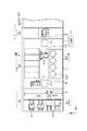
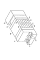
以下本発明の塗布、現像装置に露光装置を接続したレジストパターン形成装置の一例について、図面を参照しながら簡単に説明する。図1は、前記レジストパターン形成装置の一実施の形態の平面図を示し、図2は同概略斜視図である。この装置は、キャリアブロックS1と処理ブロックS2とインターフェイスブロックS3と露光装置S4とを備えている。キャリアブロックS1では、載置台21上に載置された密閉型のキャリア20から受け渡しアームCがウエハWを取り出して、当該ブロックS1に隣接された処理ブロックS2に受け渡すと共に、前記受け渡しアームCが、処理ブロックS2にて処理された処理済みのウエハWを受け取って前記キャリア20に戻すように構成されている。
Hereinafter, an example of a resist pattern forming apparatus in which an exposure apparatus is connected to the coating and developing apparatus of the present invention will be briefly described with reference to the drawings. FIG. 1 is a plan view of an embodiment of the resist pattern forming apparatus, and FIG. 2 is a schematic perspective view thereof. This apparatus includes a carrier block S1, a processing block S2, an interface block S3, and an exposure apparatus S4. In the carrier block S1, the transfer arm C takes out the wafer W from the sealed
前記処理ブロックS2は、複数個例えば6個の単位ブロックが互いに積層されるように構成され、例えば、塗布膜の形成処理を行う複数個の塗布膜形成用の単位ブロックと、現像処理を行う複数個例えば2個の現像処理用の単位ブロック(DEV1層B5、DEV2層B6)とが互いに積層されている。この例では、前記塗布膜形成用の単位ブロックとして、レジスト膜の下層側に形成される反射防止膜を形成する例えば2個の反射防止膜形成用の単位ブロック(BCT1層B1、BCT2層B2)と、レジスト膜を形成する例えば2個のレジスト膜形成用の単位ブロック(COT1層B3、COT2層B4)と、を備えている。 The processing block S2 is configured such that a plurality of, for example, six unit blocks are stacked on each other. For example, a plurality of coating film forming unit blocks for performing a coating film forming process and a plurality of developing blocks for performing a developing process are provided. For example, two unit blocks for development processing (DEV1 layer B5, DEV2 layer B6) are stacked on each other. In this example, for example, two antireflection film forming unit blocks (BCT1 layer B1, BCT2 layer B2) for forming an antireflection film formed on the lower layer side of the resist film as the unit block for forming the coating film. And, for example, two resist film forming unit blocks (COT1 layer B3, COT2 layer B4) for forming a resist film.
これらCOT1層B3,COT2層B4及びDEV1層B5,DEV2層B6はほぼ同様に構成されており、他の単位ブロックとの間でウエハWの受け渡しを行うための受け渡しモジュールやバッファモジュールが多段に配置された棚ユニットU1と、各々薬液を塗布する液処理モジュールを複数個備えた液処理モジュール群Lと、前記液処理モジュール群Lにて行われる処理の前処理及び後処理を行うための加熱・冷却系のモジュールを多段に配置した棚ユニットU2と、これら棚ユニットU1,U2の各部と液処理モジュール群Lの各モジュールとの間でウエハWの受け渡しを行なう搬送手段をなす搬送アームA3〜A6と、を備えている。 These COT1 layer B3, COT2 layer B4 and DEV1 layer B5, DEV2 layer B6 are configured in substantially the same manner, and transfer modules and buffer modules for transferring wafers W to and from other unit blocks are arranged in multiple stages. The shelf unit U1, the liquid processing module group L including a plurality of liquid processing modules each for applying a chemical solution, and heating / pretreatment for pre-processing and post-processing of the processing performed in the liquid processing module group L. A rack unit U2 in which cooling system modules are arranged in multiple stages, and transfer arms A3 to A6 serving as transfer means for transferring wafers W between the respective units of the rack units U1 and U2 and the modules of the liquid processing module group L. And.
例えば前記COT1層B3,COT2層B4、DEV1層B5、DEV2層B6は、図1にCOT1層B3を例にして示すように、図中Y方向に伸びる搬送路Rを夫々備えている。前記搬送アームA3〜A6は、当該搬送路Rにおいて、進退自在、昇降自在、鉛直軸回りに回転自在、図中Y軸方向に移動自在に構成されると共に、ウエハWの裏面側周縁領域を支持するための2本のフォークを備えており、これらフォークが互いに独立して進退できるように構成されている。 For example, the COT1 layer B3, the COT2 layer B4, the DEV1 layer B5, and the DEV2 layer B6 are each provided with a transport path R extending in the Y direction in the drawing, as shown by way of example of the COT1 layer B3 in FIG. The transfer arms A3 to A6 are configured to be movable forward and backward, vertically movable, rotatable about a vertical axis, and movable in the Y-axis direction in the figure, and supports the peripheral area on the back side of the wafer W in the transfer path R. The forks are configured to be able to advance and retreat independently of each other.
液処理モジュール群Lと棚ユニットU2とは、前記搬送路Rに沿って互いに対向するように配置されている。また液処理モジュール群Lは複数個例えば4個の液処理モジュールが搬送路Rに沿って並ぶように配列されている。これら液処理モジュールとしては、COT1層B3,COT2層B4では、レジスト液を塗布する液処理モジュールCOT、DEV1層B5,DEV2層B6では、現像液を塗布する現像モジュールDEVが夫々設けられている。 The liquid processing module group L and the shelf unit U2 are arranged along the transport path R so as to face each other. The liquid treatment module group L is arranged such that a plurality of, for example, four liquid treatment modules are arranged along the transport path R. As these liquid processing modules, a COT1 layer B3 and a COT2 layer B4 are provided with a liquid processing module COT for applying a resist solution, and a DEV1 layer B5 and a DEV2 layer B6 are provided with a developing module DEV for applying a developing solution.
前記棚ユニットU1は、図1及び図3に示すように、前記棚ユニットU1の近傍に設けられた昇降自在及び進退自在な受け渡しアームDによって当該棚ユニットU1の各部同士の間でウエハWが搬送されるように構成されている。この棚ユニットU1には、受け渡しモジュールTRSや、温調用の冷却モジュールを兼ねた受け渡しモジュールSCPW、複数枚のウエハWを載置可能なバッファと受け渡し部とを兼ねたバッファモジュールBUや、検査モジュール10等が多段に設けられている。前記棚ユニットU2には、ウエハWを加熱する加熱モジュールCPHP等が組み込まれている。なお、受け渡しモジュールTRS−Aは、キャリアブロックS1の受け渡しアームCとの間でウエハWの受け渡しを行う際に用いられるモジュールである。
As shown in FIGS. 1 and 3, the shelf unit U <b> 1 transports wafers W between the parts of the shelf unit U <b> 1 by means of a transfer arm D that can be moved up and down and moved back and forth provided in the vicinity of the shelf unit U <b> 1. It is configured to be. The shelf unit U1 includes a delivery module TRS, a delivery module SCPW that also serves as a cooling module for temperature control, a buffer module BU that serves as a buffer on which a plurality of wafers W can be placed and a delivery unit, and an
さらに、これらCOT1層B3、COT2層B4、DEV1層B5、DEV2層B6では、インターフェイスブロックB3側に棚ユニットU3が設けられている。この棚ユニットU3には各単位ブロックB3〜B6とインターフェイスブロックB3との間でウエハWの受け渡しを行うために用いられる受け渡しモジュールTRSや、前記受け渡し部とバッファとを兼ねたバッファモジュールBU、前記温調機能を備えた受け渡しモジュールSCPWが多段に設けられている。例えば棚ユニットU1に設けられたバッファモジュールBUには8枚のウエハW、棚ユニットU3に設けられたバッファモジュールBUには80枚のウエハWが、夫々載置可能に構成されている。 Further, in these COT1 layer B3, COT2 layer B4, DEV1 layer B5, and DEV2 layer B6, a shelf unit U3 is provided on the interface block B3 side. The shelf unit U3 includes a transfer module TRS used for transferring the wafer W between the unit blocks B3 to B6 and the interface block B3, a buffer module BU serving as the transfer unit and a buffer, the temperature A delivery module SCPW having an adjustment function is provided in multiple stages. For example, eight wafers W can be placed on the buffer module BU provided on the shelf unit U1, and 80 wafers W can be placed on the buffer module BU provided on the shelf unit U3.
前記、BCT1層B1,BCT2層B2は、液処理モジュールとして、レジストの下層側の反射防止膜形成用の薬液を塗布する液処理モジュールBCTが設けられ、棚ユニットU3が設けられていない以外は、COT1層B3,COT2層B4と同様に構成されている。 The BCT1 layer B1 and BCT2 layer B2 are provided as a liquid processing module, except that a liquid processing module BCT for applying a chemical solution for forming an antireflection film on the lower layer side of the resist is provided, and the shelf unit U3 is not provided. It is configured in the same manner as the COT1 layer B3 and the COT2 layer B4.
ここで、単位ブロックに設けられるモジュール群の一例について、COT1層B3を例にして説明する。棚ユニットU1には、COT1層B3へウエハを搬入するときに用いられる複数個の受け渡しモジュールSCPW31,32や、受け渡しモジュールTRS−A、BU31が設けられている。また、液処理モジュール群Lとしては、4個の液処理モジュールCOT11〜COT14を備えており、棚ユニットU2には、複数個の加熱モジュールCPHPが配列されている。さらに、棚ユニットU3には、複数個の受け渡しモジュールTRS31,32、バッファモジュールBU32が設けられている。 Here, an example of the module group provided in the unit block will be described using the COT1 layer B3 as an example. The shelf unit U1 is provided with a plurality of delivery modules SCPW31 and 32 and delivery modules TRS-A and BU31 that are used when wafers are carried into the COT1 layer B3. The liquid processing module group L includes four liquid processing modules COT11 to COT14, and a plurality of heating modules CPHP are arranged in the shelf unit U2. Further, the shelf unit U3 is provided with a plurality of delivery modules TRS31 and 32 and a buffer module BU32.
この例では、前記液処理モジュールCOT11〜COT14は、各々その内部に基板が略水平に載置される基板保持部と、この基板保持部の周囲を囲むカップを備えており、この基板保持部をモジュールと呼ぶことにする。COT1層B3に設けられる全てのモジュールは、露光前に基板に塗布膜を形成するためのモジュール群に相当する。なおこれらモジュールは全てが使用されるわけではなく、処理レシピに応じて使用されるモジュールが選択される。 In this example, each of the liquid processing modules COT11 to COT14 includes a substrate holding part on which a substrate is placed substantially horizontally and a cup surrounding the substrate holding part. We will call it a module. All the modules provided in the COT1 layer B3 correspond to a module group for forming a coating film on the substrate before exposure. Note that not all of these modules are used, and a module to be used is selected according to the processing recipe.
本発明では、ウエハWに対して同一の処理を行う複数の単位ブロックが用意されているので、2個のCOT1層B3、COT2層B4は、夫々互いに同一のモジュール群を備え、これらモジュール群を構成するモジュールや、搬送アームA3,A4の配置レイアウトが同一になるように構成されている。また、同様に2個のBCT1層B1、BCT2層B2、2個のDEV1層B5、DEV2層B6も夫々互いに同一のモジュール群を備え、これらモジュール群を構成するモジュールや、搬送アームA1,A2,A5,A6の配置レイアウトが同一になるように構成されている。 In the present invention, since a plurality of unit blocks for performing the same processing on the wafer W are prepared, the two COT1 layers B3 and COT2 layers B4 each have the same module group, and these module groups The modules to be configured and the arrangement layout of the transfer arms A3 and A4 are configured to be the same. Similarly, the two BCT1 layers B1, BCT2 layers B2, two DEV1 layers B5, and DEV2 layers B6 each have the same module group, and the modules constituting these module groups and the transport arms A1, A2, The arrangement layout of A5 and A6 is the same.
前記インターフェイスブロックS3には、インターフェイスアームEが設けられている。このインターフェイスアームEは棚ユニットU3の各受け渡しモジュールTRS、バッファモジュールBU及び露光装置S4の搬入ステージや搬出ステージにアクセスし、これらの間でウエハWを受け渡すように、昇降自在、進退自在及び鉛直軸周りに回転自在に構成されている。 An interface arm E is provided in the interface block S3. The interface arm E accesses the transfer module TRS, the buffer module BU, and the loading / unloading stage of the exposure apparatus S4 of the shelf unit U3, and can move up and down, move forward and backward, and vertically so as to transfer the wafer W between them. It is configured to be rotatable around an axis.
そして上述のレジストパターン形成装置は、各モジュールのレシピの管理や、ウエハWの搬送フロー(搬送経路)のレシピの管理、各モジュールにおける処理、受け渡しアームC、受け渡しアームD、搬送アームA1〜A6、インターフェイスアームE等の駆動制御を行うコンピュータからなる制御部3を備えている。この制御部3は、レジストパターン形成装置全体の作用、つまりウエハWに対して所定のレジストパターンを形成するための、各モジュールにおける処理やウエハWの搬送等が実施されるようにステップ(命令)群を備えた例えばソフトウェアからなるプログラムを備えている。そしてこれらプログラムが制御部3に読み出されることにより、制御部によってレジストパターン形成装置全体の作用が制御される。なおこのプログラムは、例えばフレキシブルディスク、ハードディスク、コンパクトディスク、マグネットオプティカルディスク、メモリーカード等の記憶媒体に収納された状態で格納される。
The resist pattern forming apparatus described above manages the recipe of each module, manages the recipe of the transfer flow (transfer path) of the wafer W, processes in each module, the transfer arm C, the transfer arm D, the transfer arms A1 to A6, A
図4は制御部3の構成を示すものであり、実際にはCPU(中央モジュール)、プログラム及びメモリなどにより構成されるが、本発明ではモジュールが使用不可になったときのウエハWの搬送に特徴があるので、ここではそれに関連する構成要素の一部をブロック化して説明するものとする。図4中30はバスであり、このバス30にレシピ格納部31、レシピ選択部32、搬送スケジュール変更部33、搬送制御部34、搬送制御プログラム35、アラーム発生手段36等が接続されている。
FIG. 4 shows the configuration of the
また、各モジュールMはコントローラC0を介して制御部3に接続されており、各々のモジュールMにてトラブルが発生したときには、当該モジュールMからコントローラC0を介して制御部3にアラーム信号が出力されるようになっている。さらに、ウエハが所定のタイミングで受け渡しアームDや搬送アームA1〜A6に受け渡されない場合にも、制御部3にアラーム信号が出力されるようになっている。なお、前記モジュールMには、例えば棚ユニットU1〜U3に組み込まれた全てのモジュールと、液処理モジュールとが含まれる。
Each module M is connected to the
レシピ格納部31は記憶部に相当する部位であり、例えばウエハWの搬送経路が記録されている搬送レシピや、この搬送レシピに基づき、ロット内の全てのウエハWについてどのタイミングでどのモジュールに搬送するかといった内容の搬送スケジュールや、ウエハWに対して行う処理条件などが記録された複数のレシピが格納される部位である。レシピ選択部32はレシピ格納部31に格納されたレシピから適当なものを選択する部位であり、使用するモジュールMの選択等もできるようになっている。
The
搬送スケジュール変更部33は、ウエハWの搬送中に、当該ウエハWの搬送予定のモジュールが使用不可モジュールとなったときに、後述するように搬送スケジュールを書き換える部位である。搬送制御部34は、前記搬送スケジュールを参照し、搬送サイクルデータに書き込まれているウエハを、そのウエハに対応するモジュールに搬送するように、受け渡しアームCや受け渡しアームD、搬送アームA1〜A6、インターフェイスアームEを制御し、これにより搬送サイクルを実行する手段である。
搬送制御プログラム35は、ウエハWの搬送中に、当該ウエハWの搬送予定のモジュールが使用不可モジュールとなったときに駆動するプログラムである。このプログラムは、例えばモジュールにてトラブルが発生したり、ウエハWの搬送が乱れたりしたときに発生されるアラーム信号に基づいて駆動される。また、オペレータがコンピュータの表示画面により、使用不可モジュールを選択することによっても駆動されるようになっている。この使用不可モジュールとは、モジュールにトラブルが発生したか、メンテナンス等により、ウエハを搬入できないモジュールをいう。また、オペレータが使用不可モジュールを選択するときとは、モジュールにメンテナンスを行う場合や、プロセスが正常にできないモジュールを使用不可モジュールとする場合等が含まれる。ここでプロセスが正常にできないとは他のマルチモジュールとの差が発生する場合をいう。このような場合、当該モジュールを使用しないようにレシピを変更すると、当該モジュールが正常に戻った場合再度レシピを変更しなければならず、レシピが複数存在するとそのレシピ数分作業が発生するため、使用不可モジュールとすることが好ましい。
The transfer
The
そして、使用不可モジュールが発生し、後述する搬送制御が実施可能であるときには、例えばコンピュータの表示画面に使用不可モジュールが発生した旨を表示し、受け渡しアームC、受け渡しアームD、搬送アームA1〜A6、インターフェイスアームEを制御すると共に、搬送スケジュールの変更を行って後述の搬送制御を実施する。一方、使用不可モジュールが発生した場合であっても、後述する搬送制御が実施不可能であるときには、アラーム発生手段36によりアラームを出力すると共に、装置を停止する。このアラーム発生手段36によっては、ランプの点灯やアラーム音の発生、表示画面へのアラーム表示等のアラーム発生が行われる。 Then, when an unusable module is generated and transfer control described later can be performed, for example, a message indicating that the unusable module has occurred is displayed on the display screen of the computer, and the transfer arm C, the transfer arm D, and the transfer arms A1 to A6 are displayed. In addition to controlling the interface arm E, the conveyance schedule is changed to carry out conveyance control described later. On the other hand, even when the unusable module is generated, if the conveyance control described later cannot be performed, the alarm generation means 36 outputs an alarm and stops the apparatus. Depending on the alarm generation means 36, an alarm is generated such as lighting of a lamp, generation of an alarm sound, and alarm display on a display screen.
ここで、搬送制御が実施可能であるときとは、マルチモジュールを構成する複数のモジュールの少なくとも一つが使用できる状態にある場合をいう。この際、マルチモジュールとは、ウエハが各々載置されると共に搬送の順番が決められているモジュール群の中で、搬送の順番が同じであって、ウエハに対して同一の処理を行う複数のモジュール、つまり搬送レシピの同じステップに設定された複数のモジュールをいう。一方、搬送制御が実施不可能であるときとは、搬送レシピの同じステップに一つのモジュールしか設定されていない場合や、搬送レシピの同じステップに複数のモジュールが設定されているが、使用できる状態にあるモジュールがない場合である。 Here, the case where the conveyance control can be performed means a case where at least one of a plurality of modules constituting the multi-module is in a usable state. In this case, the multi-module is a plurality of modules in which the wafers are placed and the transfer order is determined, and the transfer order is the same, and the wafers are subjected to the same processing. A module, that is, a plurality of modules set in the same step of the transfer recipe. On the other hand, when transfer control is not possible, when only one module is set in the same step of the transfer recipe, or when multiple modules are set in the same step of the transfer recipe, it can be used. This is the case when there is no module.
続いて、ウエハに対して同一の処理を行う複数の単位ブロックがCOT1層B3とCOT2層B4である場合を例にして、本発明の搬送制御について具体的に説明する。先ず、前記レジストパターン形成装置での通常時のウエハWの流れの一例について説明する。キャリアブロックS1からのウエハWは受け渡しアームCにより、棚ユニットU1の受け渡しモジュールSCPW、例えばBCT1層B1、BCT2層B2の対応する受け渡しモジュールSCPW11,12、SCPW21,22に順次搬送される。この場合、BCT層は2層であるので、ロット内のウエハWは、先頭から順にBCT1層B1と、BCT2層B2に交互に搬送され、例えば奇数番のウエハW(2n+1)はBCT1層B1へ、偶数番のウエハW2nはBCT2B2層へ夫々払い出される。 Subsequently, the conveyance control of the present invention will be specifically described by taking as an example the case where a plurality of unit blocks that perform the same processing on the wafer are the COT1 layer B3 and the COT2 layer B4. First, an example of the flow of the wafer W at the normal time in the resist pattern forming apparatus will be described. The wafer W from the carrier block S1 is sequentially transferred by the transfer arm C to the transfer module SCPW of the shelf unit U1, for example, the transfer modules SCPW11, 12 and SCPW21, 22 corresponding to the BCT1 layer B1 and BCT2 layer B2. In this case, since there are two BCT layers, the wafers W in the lot are alternately transferred to the BCT1 layer B1 and the BCT2 layer B2 in order from the top. For example, the odd-numbered wafers W (2n + 1) are BCT1 layers. to B1, the wafer W 2n even-numbered are each paid out to BCT2B2 layer.
BCT層B1(B2)内では、ウエハWは搬送アームA1(A2)により、液処理モジュールBCT→加熱モジュールCPHP→棚ユニットU1の受け渡しモジュールTRS11,12(TRS21,22)の経路で搬送され、ウエハWには反射防止膜が形成される。 Within the BCT layer B1 (B2), the wafer W is transferred by the transfer arm A1 (A2) along the path of the liquid processing module BCT → the heating module CPHP → the delivery module TRS11, 12 (TRS21, 22) of the shelf unit U1. An antireflection film is formed on W.
その後、例えばBCT層B1(B2)のウエハWは、棚ユニットU1内において受け渡しアームDにより受け渡しモジュールTRS11,12(TRS21,22)から受け渡しモジュールSCPW31,32(SCPW41,42)に搬送され、このウエハWは搬送アームA3(A4)により、COT層B3(B4)内に受け渡される。そして、COT層B3(B4)内において、液処理モジュールCOT→加熱モジュールCPHP→棚ユニットU3の受け渡しモジュールTRS31,32(TRS41,42)の経路で搬送され、ウエハWには反射防止膜の上にレジスト膜が形成される。 Thereafter, for example, the wafer W of the BCT layer B1 (B2) is transferred from the transfer modules TRS11, 12 (TRS21, 22) to the transfer modules SCPW31, 32 (SCPW41, 42) by the transfer arm D in the shelf unit U1. W is transferred into the COT layer B3 (B4) by the transfer arm A3 (A4). Then, in the COT layer B3 (B4), the liquid processing module COT → the heating module CPHP → the shelf unit U3 is transported by the path of the delivery modules TRS31 and 32 (TRS41 and 42), and is placed on the antireflection film on the wafer W. A resist film is formed.
そして、棚ユニットU3の受け渡しモジュールTRS31,32、TRS41,42のウエハWは、インターフェイスブロックS3のインターフェイスアームEにより露光装置S4の搬入ステージに搬送され、所定の露光処理が行われた後、露光装置S4の搬出ステージからインターフェイスアームEにより棚ユニットU3の受け渡しモジュールSCPW51,52、SCPW61,62に載置される。この例では、例えば奇数番のウエハW(2n+1)は前記受け渡しモジュールSCPW51,52へ、偶数番のウエハW(2n)は前記受け渡しモジュールSCPW61,62へ夫々払い出される。 Then, the wafers W of the delivery modules TRS31 and 32 and TRS41 and 42 of the shelf unit U3 are transferred to the carry-in stage of the exposure apparatus S4 by the interface arm E of the interface block S3, and after performing a predetermined exposure process, the exposure apparatus It is mounted on the delivery modules SCPW51, 52, SCPW61, 62 of the shelf unit U3 by the interface arm E from the unloading stage of S4. In this example, for example, odd-numbered wafers W (2n + 1) are delivered to the delivery modules SCPW51 and 52, and even-numbered wafers W (2n) are delivered to the delivery modules SCPW61 and 62, respectively.
次いで、受け渡しモジュールSCPW51,52(SCPW61,62)のウエハWは、搬送アームA5(A6)によりDEV層B5(B6)へ受け取られ、DEV層B5(B6)内では、液処理モジュールDEV→加熱モジュールCPHP→棚ユニットU1の受け渡しモジュールTRS51,52(TRS61,62)の経路で搬送される。そして、ウエハWは、検査モジュール10に搬送される場合には、受け渡しアームDにより、キャリア20から払い出された順番に沿って検査モジュール10に搬送して所定の検査を行い、次いで、受け渡しアームDにより、キャリア20から払い出された順番に沿って受け渡しモジュールTRS―Aに搬送する。この後、受け渡しアームCにより、キャリア20から払い出された順番に沿ってキャリア20に戻される。また、検査モジュール10に搬送しない場合には、受け渡しアームDにより、キャリア20から払い出された順番に沿って、受け渡しモジュールTRS―Aに搬送し、この後、受け渡しアームCにより、キャリア20から払い出された順番に沿ってキャリア20に戻される。
Next, the wafers W of the delivery modules SCPW51, 52 (SCPW61, 62) are received by the transfer arm A5 (A6) to the DEV layer B5 (B6), and in the DEV layer B5 (B6), the liquid processing module DEV → the heating module. CPHP is transported along the path of the delivery modules TRS 51 and 52 (TRS 61 and 62) of the shelf unit U1. Then, when the wafer W is transferred to the
この際、ウエハWは、各単位ブロックB1〜B6における夫々のモジュール群に対して、後述の搬送スケジュールに従って搬送アームA1〜A6によりウエハWの搬送が行われる。つまり、各単位ブロックB1〜B6では、各々の搬送アームA1〜A6により、夫々のモジュール群において、一のモジュールからウエハWを取り出し、次のモジュールのウエハWを受け取ってから当該次のモジュールに先のウエハWを受け渡し、こうして各モジュールに置かれたウエハWを一つ順番が後のモジュールに移すことにより一の搬送サイクルを実行し、当該一の搬送サイクルを実行した後、次の搬送サイクルに移行し、各搬送サイクルを順次実行することにより前記モジュール群のうち順番の小さいモジュールから順番の大きいモジュールにウエハWが順次搬送されて所定の処理が行われるようになっている。 At this time, the wafer W is transferred to the module groups in the unit blocks B1 to B6 by the transfer arms A1 to A6 according to the transfer schedule described later. That is, in each of the unit blocks B1 to B6, the wafer W is taken out from one module in each module group by the transfer arms A1 to A6, and the wafer W of the next module is received before the next module. The wafer W is transferred, and the wafer W placed in each module is transferred to the next module in order, thereby executing one transfer cycle. After executing the one transfer cycle, the next transfer cycle is started. By shifting and sequentially executing each transfer cycle, the wafer W is sequentially transferred from the module with the smallest order to the module with the largest order in the module group, and a predetermined process is performed.
ここで各単位ブロックB1〜B6内では、搬送アームA1〜A6は、搬入モジュールをなす受け渡しモジュールSCPWからウエハを受け取り、当該ウエハを既述の搬送経路に沿って、順次前記搬送サイクルの下流端の搬出モジュールである受け渡しモジュールTRSまで搬送し、こうして単位ブロックB1〜B6内にて夫々搬送サイクルを行うように構成されている。 Here, in each of the unit blocks B1 to B6, the transfer arms A1 to A6 receive the wafer from the delivery module SCPW that forms the carry-in module, and sequentially transfer the wafer along the transfer path described above to the downstream end of the transfer cycle. It conveys to the delivery module TRS which is a carrying-out module, and is comprised so that a conveyance cycle may be performed in unit block B1-B6, respectively.
既述の搬送では、COT1層B3(COT2層B4)における搬送レシピは、ステップ1では、2個の受け渡しモジュールSCPW31,32(SCPW41,4)、ステップ2では2個の液処理モジュールCOT11,12(COT21,22)、ステップ3では4個の加熱モジュールCPHP31〜34(CPHP41〜44)、ステップ4では2個の受け渡しモジュールTRS31,32(TRS41,42)が夫々設定されるものとする。従って、COT1層B3(COT2層B4)では、受け渡しモジュールSCPW31,32(SCPW41,42)、液処理モジュールCOT11,12(COT21,22)、加熱モジュールCPHP31〜34(CPHP41〜44)、受け渡しモジュールTRS31,32(TRS41,42)が夫々マルチモジュールとして設定されている。
In the transfer described above, the transfer recipe in the COT1 layer B3 (COT2 layer B4) is as follows. In
ここで、COT1層B3、COT2層B4における通常時の搬送制御の一例について、より詳しく図5を用いて説明する。キャリア20からロットの(4n−3)番目つまり1番目、5番目・・・に払い出されたウエハW(4n−3)は受け渡しモジュールSCPW11→BCT1層B1→受け渡しモジュールTRS11→受け渡しモジュールSCPW31の系路でCOT1層B3に搬送され、レジスト膜が形成された後、受け渡しモジュールTRS31に搬送される。同様に、キャリア20からロットの(4n−2)番目つまり2番目、6番目・・・に払い出されたウエハW(4n−2)は受け渡しモジュールSCPW21→BCT2層B2→受け渡しモジュールTRS21→受け渡しモジュールSCPW41の系路でCOT2層B4に搬送され、レジスト膜が形成された後、受け渡しモジュールTRS41に搬送される。
Here, an example of normal conveyance control in the COT1 layer B3 and the COT2 layer B4 will be described in more detail with reference to FIG. The wafer W (4n-3) delivered from the
また、キャリア20からロットの(4n−1)番目つまり3番目、7番目・・・に払い出されたウエハW(4n−1)は受け渡しモジュールSCPW12→BCT1層B1→受け渡しモジュールTRS12→受け渡しモジュールSCPW32の系路でCOT1層B3に搬送され、レジスト膜が形成された後、受け渡しモジュールTRS32に搬送される。さらに、キャリア20からロットの4n番目つまり4番目、8番目・・・に払い出されたウエハW4nは受け渡しモジュールSCPW22→BCT2層B2→受け渡しモジュールTRS22→受け渡しモジュールSCPW42の系路でCOT2層B4に搬送され、レジスト膜が形成された後、受け渡しモジュールTRS42に搬送される。この場合、受け渡しモジュールTRS31,32,41,42には、キャリア20から払い出された順番に沿って、ウエハWが搬送される。
Further, the wafer W (4n-1) delivered from the
そして、各受け渡しモジュールTRS31,32,41,42のウエハWは、インターフェイスアームEにより、キャリア20から払い出された順番に沿って露光装置S4の搬入ステージに搬送される。この際、露光装置S4の搬入ステージが搬入可能であればそのまま搬送され、搬入可能でなければ、一旦バッファモジュールBU32,BU42に搬送される。露光装置S4の搬入ステージが搬入可能ではない場合とは、露光装置S4側が処理ブロックS2よりもスループットが小さく、露光装置S4への搬入ステージに搬送順番が若いウエハWが存在する場合である。
Then, the wafers W of the transfer modules TRS31, 32, 41, and 42 are transferred by the interface arm E to the carry-in stage of the exposure apparatus S4 in the order in which they are discharged from the
このときの搬送スケジュールのシミュレーション例について、COT1層B3は図6、COT2層B4は図7に夫々示す。この搬送スケジュールでは、縦軸は搬送サイクル、横軸はモジュール群を構成するモジュールを夫々示し、受け渡しモジュールSCPW31,32(SCPW41,42)が搬入モジュール、受け渡しモジュールTRS31,32(TRS41,42)が搬出モジュールに夫々相当する。また、W1はロットの1番目のウエハ、W2はロットの2番目にウエハを夫々示している。この搬送スケジュールの右側に書かれた数字は、夫々の搬送サイクルが開始されてから終了するまでの時間である。また、このシミュレーション結果では、ロットの最初のウエハW1が受け渡しモジュールSCPW31に載置されてから、ロットの最終のウエハW50が受け渡しモジュールTRS42に載置されるまでの時間は783.4秒である。 Regarding the simulation example of the transport schedule at this time, FIG. 6 shows the COT1 layer B3 and FIG. 7 shows the COT2 layer B4. In this transfer schedule, the vertical axis indicates the transfer cycle, and the horizontal axis indicates the modules constituting the module group. The delivery modules SCPW31 and 32 (SCPW41 and 42) are the carry-in modules, and the transfer modules TRS31 and 32 (TRS41 and 42) are carried out. Each corresponds to a module. W1 represents the first wafer of the lot, and W2 represents the second wafer of the lot. The number written on the right side of the transfer schedule is the time from the start to the end of each transfer cycle. In this simulation result, the time from when the first wafer W1 of the lot is placed on the delivery module SCPW31 to when the last wafer W50 of the lot is placed on the delivery module TRS42 is 783.4 seconds.
この際、受け渡しアームDはBCT1層B1又はBCT2層B2から搬出されたウエハWを、最も早く搬送可能になった搬入モジュールSCPW31,32,41,42に搬送し、ウエハWが搬入モジュールSCPW31,32,41,42からモジュール群の最初のモジュールである液処理モジュールCOTに受け渡されたときに搬送サイクルが開始される。そして、通常時には、既述の図5に示すように、ウエハWがキャリア20から払い出された順番に沿って、1番目のウエハWから順に搬入モジュールSCPW31,SCPW41,SCPW32,SCPW42に搬入されるようになっている。
At this time, the transfer arm D transports the wafer W carried out of the BCT1 layer B1 or BCT2 layer B2 to the carry-in modules SCPW31, 32, 41, 42 that can be carried most quickly, and the wafer W is loaded into the carry-in modules SCPW31, 32. , 41, 42 are transferred to the liquid processing module COT which is the first module of the module group, and the transfer cycle is started. In the normal state, as shown in FIG. 5 described above, the wafers W are loaded into the loading modules SCPW31, SCPW41, SCPW32, and SCPW42 sequentially from the first wafer W in the order in which the wafers W are discharged from the
続いて、COT1層B3において、加熱モジュールCPHPの一つが使用不可モジュールとなりかつ少なくとも一つが使用できる状態にあるときの搬送制御の一例について、図8〜図10を用いて説明する。この場合、前記搬送制御プログラム35により、図8に示すような搬送制御が行われる。つまり、使用不可モジュールが発生すると(ステップS1)、第1の受け渡し手段をなす受け渡しアームDにより、COT1層B3及びCOT2層B4において、最も早く載置可能になった搬入モジュール(受け渡しモジュールSCPW31,32,41,42)にウエハWを払い出す(ステップS2)。ここで最も早く載置可能になるとは、受け渡しモジュールSCPWに置かれた前のウエハが搬送アームA3,A4により受け取られたタイミングが最も早いことをいう。
Subsequently, an example of the conveyance control when one of the heating modules CPHP becomes an unusable module and at least one is usable in the COT1 layer B3 will be described with reference to FIGS. In this case, the conveyance control as shown in FIG. 8 is performed by the
そして、COT1層B3及びCOT2層B4の夫々においては、ウエハWが搬入モジュール(受け渡しモジュールSCPW31,32,41,42)に払い出された順番に沿って、搬送アームA3,A4によりウエハWをモジュール群に順次搬送して搬出モジュール(受け渡しモジュールTRS31,32,41,42)に受け渡す(ステップS3)。
In each of the COT1 layer B3 and the COT2 layer B4, the wafers W are moduled by the transfer arms A3, A4 in the order in which the wafers W are delivered to the carry-in modules (delivery modules SCPW31, 32, 41, 42). It is sequentially transported to the group and delivered to the carry-out module (
次いで、ウエハWが搬入モジュール(受け渡しモジュールSCPW31,32,41,42)に払い出された順番に沿って、第2の受け渡し手段であるインターフェイスアームEによりウエハWを搬出モジュール(受け渡しモジュールTRS31,32,41,42)から取り出し、後段モジュールである露光装置S4又は基板載置部であるバッファモジュールBU32,42に搬送する(ステップS4)。 Next, in accordance with the order in which the wafers W are delivered to the delivery modules (delivery modules SCPW31, 32, 41, 42), the wafer W is delivered by the interface arm E as the second delivery means (delivery modules TRS31, 32). , 41, 42) and transported to the exposure apparatus S4, which is a subsequent module, or the buffer modules BU32, 42, which is a substrate placement unit (step S4).
この後、通常時に第1の受け渡し手段(受け渡しアームD)によりウエハWがCOT1層B3及びCOT2層B4の搬入モジュール(受け渡しモジュールSCPW31,32,41,42)に払い出される一定の順番に沿って、第2の受け渡し手段(インターフェイスアームE)により搬出モジュール(受け渡しモジュールTRS31,32,41,42)又はバッファモジュールBU32,42から露光装置S4の搬入ステージにウエハWを搬送する(ステップS5)。 Thereafter, the wafer W is normally delivered to the COT1 layer B3 and the COT2 layer B4 loading modules (delivery modules SCPW31, 32, 41, 42) by the first delivery means (delivery arm D) at normal times. The wafer W is transferred from the transfer module (transfer module TRS31, 32, 41, 42) or the buffer module BU32, 42 to the transfer stage of the exposure apparatus S4 by the second transfer means (interface arm E) (step S5).
実際には図9に示すフローチャートに従って搬送制御が実行される。使用不可モジュールの発生前は、COT1層B3及びCOT2層B4では、通常時の搬送スケジュールに沿って夫々ウエハWの搬送が行われる(ステップS10)。COT1層B3の加熱モジュールCPHP31にトラブルが発生して、当該モジュールが使用不可モジュールとなると(ステップS11)、当該加熱モジュールCPHP31にウエハWを搬送しないように搬送スケジュールが書き換えられる(ステップS12)。 Actually, the conveyance control is executed according to the flowchart shown in FIG. Before the unusable module is generated, the wafer W is transferred in the COT1 layer B3 and the COT2 layer B4 according to the normal transfer schedule (step S10). When a trouble occurs in the heating module CPHP31 of the COT1 layer B3 and the module becomes an unusable module (step S11), the transfer schedule is rewritten so as not to transfer the wafer W to the heating module CPHP31 (step S12).
そして、使用不可モジュールが発生した後に、COT1層B3及びCOT2層B4に搬入されるウエハWは、受け渡しアームDにより、搬入モジュール(受け渡しモジュールSCPW31,32,41,42)の内、最も早く載置可能になったモジュールに搬送する(ステップS13)。 Then, after the unusable module is generated, the wafer W carried into the COT1 layer B3 and the COT2 layer B4 is placed by the delivery arm D earliest among the delivery modules (delivery modules SCPW31, 32, 41, 42). It is transported to the module that has become possible (step S13).
ウエハWが搬入モジュールに載置されると、当該搬入モジュールが、搬送スケジュールに記載された搬入モジュールと同じか否かを判断し(ステップS14)、同じ場合には、搬送スケジュールに従って、COT1層B3又はCOT2層B4内においてウエハWの搬送を1サイクル分実行する(ステップS15)。 When the wafer W is placed on the carry-in module, it is determined whether or not the carry-in module is the same as the carry-in module described in the transfer schedule (step S14). If the same, the COT1 layer B3 is determined according to the transfer schedule. Alternatively, the wafer W is transferred for one cycle within the COT2 layer B4 (step S15).
一方、ウエハWが載置された搬入モジュールが、搬送スケジュールに記載された搬入モジュールと異なる場合には、前記搬入モジュールに搬入されたウエハWが当該搬送サイクルにて搬入モジュールに置かれるウエハWと同じになるように、前記搬送スケジュールを書き換える(ステップS16)。そして、書き換えられた搬送スケジュールに従って、COT1層B3又はCOT2層B4内においてウエハWの搬送を1サイクル実行する(ステップS17)。 On the other hand, when the carry-in module on which the wafer W is placed is different from the carry-in module described in the transfer schedule, the wafer W loaded into the carry-in module is placed on the carry-in module in the transfer cycle. The transport schedule is rewritten so as to be the same (step S16). Then, according to the rewritten transfer schedule, the transfer of the wafer W in the COT1 layer B3 or the COT2 layer B4 is executed for one cycle (step S17).
次いで、当該ウエハWがロットの最終のウエハか否かを判断し(ステップS18)、最終ウエハである場合には、当該搬送スケジュールに従ってウエハWの搬送を実行する(ステップS10)、最終ウエハではない場合には、当該ウエハの次にBCT1層B1又はBCT2層B2から払い出されたウエハWについて、ステップS13から同様に搬送を実行する(ステップS20)。 Next, it is determined whether or not the wafer W is the final wafer of the lot (step S18). If the wafer W is the final wafer, the wafer W is transferred according to the transfer schedule (step S10) and is not the final wafer. In this case, the wafer W discharged from the BCT1 layer B1 or BCT2 layer B2 next to the wafer is transferred in the same manner from step S13 (step S20).
こうして、COT1層B3、COT2層B4の夫々においては、搬送スケジュールに従って、ウエハWが搬入モジュールに払い出された順番に沿って順次搬送して搬出モジュール(受け渡しモジュールTRS31,32,41,42)に受け渡す。そして、この搬出モジュール(受け渡しモジュールTRS31,32,41,42)のウエハWは、既述のように、インターフェイスアームEにより、ウエハWが搬入モジュールに払い出された順番に沿って取り出される。
In this way, in each of the COT1 layer B3 and the COT2 layer B4, the wafers W are sequentially transferred according to the transfer schedule in the order in which they are discharged to the loading module, and are transferred to the unloading modules (delivery modules TRS31, 32, 41, 42). Deliver. Then, the wafer W of the carry-out module (
次いで、ウエハWは、インターフェイスアームEによりキャリア20から払い出された順番に沿って露光装置S4の搬入ステージに搬送される。つまり、搬出モジュール(受け渡しモジュールTRS31,32,41,42)のウエハWが、露光装置S4の搬入ステージに搬送される順番であれば、そのまま前記搬入ステージに搬送され、前記順番でなければ一旦バッファモジュールBU31,41に搬送される。そして、インターフェイスアームEにより、搬出モジュール(受け渡しモジュールTRS31,32,41,42)から直接、又はバッファモジュールBU31,41を介して露光装置S4の搬入ステージに、通常時に受け渡しアームDによりCOT1層B3及びCOT2層B4にウエハWが払い出される一定の順番に沿ってウエハWを搬送する。
Next, the wafer W is transferred to the loading stage of the exposure apparatus S4 along the order in which the wafer W is discharged from the
このときの搬送スケジュールのシミュレーション結果について、COT1層B3は図11、COT2層B4を図12に夫々示す。この搬送スケジュールでは、COT2層B4において、サイクル19にてロットの41番目のウエハW41が受け渡しモジュールSCPW41に搬送されたとき、サイクル21にてロットの44番目のウエハW44が受け渡しモジュールSCPW41に搬送されたとき、サイクル24にてロットの49番目のウエハW49が受け渡しモジュールSCPW42に搬送されたときに、夫々搬送スケジュールが書き換えられている。また、このシミュレーション結果によれば、最初のウエハW1が受け渡しモジュールSCPW31に載置されてから、最終ウエハW50が受け渡しモジュールTRS32に載置されるまでの時間は843.4秒である。
As for the simulation result of the conveyance schedule at this time, FIG. 11 shows the COT1 layer B3 and FIG. 12 shows the COT2 layer B4. In this transfer schedule, when the 41st wafer W41 of the lot is transferred to the delivery module SCPW41 in the
上述の実施の形態によれば、COT1層B3の加熱モジュールCPHPの一つが使用不可モジュールとなったとしても、当該COT1層B3の他の加熱モジュールCPHPが使用可能である場合は、COT1層B3及びCOT2層B4の搬入モジュール(受け渡しモジュールSCPW31,32,41,42)の内、最も早く載置可能になった搬入モジュールに搬入している。 According to the above-described embodiment, even if one of the heating modules CPHP of the COT1 layer B3 becomes an unusable module, when another heating module CPHP of the COT1 layer B3 is usable, the COT1 layer B3 and Of the carry-in modules (delivery modules SCPW31, 32, 41, 42) of the COT2 layer B4, they are carried into the carry-in module that can be mounted earliest.
このため、加熱モジュールCPHPの一つが使用不可モジュールになったとしても、COT1層B3及びCOT2層B4に交互にウエハWを搬入する場合に比べて、スループットの低下を抑えることができる。搬入モジュールが空いた単位ブロックに順次ウエハが払い出されるので、使用可能な加熱モジュールCPHPがウエハWの搬送を待機するといったことが抑えられ、使用可能な加熱モジュールCPHPの稼働効率の低下を抑制できるからである。 For this reason, even if one of the heating modules CPHP becomes an unusable module, a decrease in throughput can be suppressed as compared with the case where wafers W are alternately loaded into the COT1 layer B3 and the COT2 layer B4. Since the wafers are sequentially dispensed to the unit block in which the carry-in module is empty, it is possible to prevent the usable heating module CPHP from waiting for the transfer of the wafer W, and it is possible to suppress a decrease in the operating efficiency of the usable heating module CPHP. It is.
これに対して、COT1層B3及びCOT2層B4に交互にウエハWを搬入する場合には、使用不可モジュールが発生していないCOT2層B4において、使用不可モジュールが発生したCOT1層B3へのウエハWの搬入や、COT1層B3からのウエハWの搬出を待機する必要があり、COT2層B4において、搬送可能な加熱モジュールCPHPにウエハWが搬送されずに、稼働率が低くなり、スループットが低下してしまう。 On the other hand, when the wafer W is alternately loaded into the COT1 layer B3 and the COT2 layer B4, the wafer W to the COT1 layer B3 where the unusable module is generated in the COT2 layer B4 where the unusable module is not generated. In the COT2 layer B4, the wafer W is not transferred to the transferable heating module CPHP, the operating rate is lowered, and the throughput is reduced. End up.
ここで、COT1層B3の加熱モジュールCPHP31が使用不可モジュールになったときに、COT1層B3及びCOT2層B4に交互にウエハを払い出す場合の搬送スケジュールのシミュレーション結果について、COT1層B3を図13に、COT2層B4を図14に夫々示す。このシミュレーション結果によれば、最初のウエハW1が受け渡しモジュールSCPW31に載置されてから、最終ウエハW50が受け渡しモジュールTRS42に載置されるまでの時間は891.7秒であり、本発明の搬送制御に比べてスループットが低いことが理解される。 Here, FIG. 13 shows the simulation result of the transfer schedule when the wafer is alternately delivered to the COT1 layer B3 and the COT2 layer B4 when the heating module CPHP31 of the COT1 layer B3 becomes an unusable module. COT2 layer B4 is shown in FIG. According to this simulation result, the time from when the first wafer W1 is placed on the delivery module SCPW31 to when the final wafer W50 is placed on the delivery module TRS42 is 891.7 seconds. It is understood that the throughput is low compared to
この際、本発明では、ウエハがCOT1層B3、COT2層B4に交互に搬送されるわけではないので、一方のCOT層の搬出モジュールから連続した順番でウエハWが払い出されることもあるが、COT1層B3及びCOT2層B4の搬出モジュールの下流側に設けられたバッファモジュールBU32,42を利用して、露光装置S4に搬送される前にウエハWを一旦整列させているので、キャリア20からウエハWが払い出される順番で露光装置S4に搬送することができる。
At this time, in the present invention, since the wafers are not alternately transferred to the COT1 layer B3 and the COT2 layer B4, the wafers W may be discharged in a continuous order from the unloading module of one COT layer. Since the buffer modules BU32 and 42 provided on the downstream side of the unloading modules of the layer B3 and the COT2 layer B4 are used to temporarily align the wafer W before being transferred to the exposure apparatus S4, the wafer W is transferred from the
従って、COT1層B3,COT2層B4の夫々では、搬入モジュール(受け渡しモジュールSCPW31,32,41,42)に払い出された順番に沿ってウエハが搬送され、そのまま搬出モジュール(受け渡しモジュールTRS31,32,41,42)に搬送されるので、COT層B3,COT2層B4内において、ウエハの搬送順番が入れ替わるといったことがなく、搬送制御の複雑化が抑えられる。 Accordingly, in each of the COT1 layer B3 and the COT2 layer B4, the wafers are transferred in the order delivered to the carry-in module (delivery module SCPW31, 32, 41, 42), and the carry-out module (delivery module TRS31, 32, 41, 42), the wafer transfer order is not changed in the COT layer B3, COT2 layer B4, and the complexity of the transfer control is suppressed.
続いて、他の単位ブロックにおける搬送例について説明する。図15は、BCT1層B1、BCT2層B2のいずれかのマルチモジュールの少なくとも一つが使用不可モジュールになりかつ少なくとも一つが使用できる状態にあるときに、COT1層B3、COT2層B4に搬送する前に、一旦ウエハWをキャリア20から払い出された順番に整列させる場合の搬送例である。
Subsequently, a conveyance example in another unit block will be described. FIG. 15 shows that when at least one of the multi-modules of the BCT1 layer B1 and the BCT2 layer B2 becomes an unusable module and at least one is in a usable state, before being transferred to the COT1 layer B3 and the COT2 layer B4. In this example, the wafers W are once aligned in the order in which they are discharged from the
この場合、第1の受け渡し手段をなす受け渡しアームCにより、BCT1層B1,BCT2層B2において最も早く載置可能になった搬入モジュール(受け渡しモジュールSCPW11,12,21,22)にウエハWを払い出す。そして、BCT1層B1、BCT2層B2の夫々においては、ウエハWが搬入モジュール(受け渡しモジュールSCPW11,12,21,22)に払い出された順番に沿って、搬送アームA1,A2によりウエハWをモジュール群に順次搬送して搬出モジュール(受け渡しモジュールTRS11,12,21,22)に受け渡す。 In this case, the transfer arm C serving as the first transfer means delivers the wafer W to the carry-in module (the transfer modules SCPW11, 12, 21, 22) that can be placed first in the BCT1 layer B1 and the BCT2 layer B2. . In each of the BCT1 layer B1 and the BCT2 layer B2, the wafers W are moduled by the transfer arms A1 and A2 in the order in which the wafers W are delivered to the carry-in modules (delivery modules SCPW11, 12, 21, and 22). It is sequentially conveyed to the group and delivered to the carry-out module (delivery modules TRS11, 12, 21, 22).
次いで、ウエハWが搬入モジュール(受け渡しモジュールSCPW11,12,21,22)に払い出された順番に沿って、第2の受け渡し手段をなす受け渡しアームDによりウエハWを搬出モジュール(受け渡しモジュールTRS11,12,21,22)から取り出し、後段モジュールであるCOT1層B3、COT2層B4の受け渡しモジュールSCPW31,32,41,42又は基板載置部であるバッファモジュールBU1,BU2に搬送する。 Next, along the order in which the wafers W are delivered to the delivery modules (delivery modules SCPW11, 12, 21, 22), the delivery arm D serving as the second delivery means delivers the wafer W (delivery modules TRS11, 12). , 21, 22) and transported to COT1 layer B3 and COT2 layer B4 delivery modules SCPW31, 32, 41, and 42 or buffer modules BU1 and BU2 as substrate mounting units.
続いて、通常時に受け渡しアームCによりウエハWがBCT1層B1,BCT2層B2の受け渡しモジュールSCPW11,12,21,22に払い出される一定の順番に沿って、受け渡しアームDにより搬出モジュール(受け渡しモジュールTRS11,12,21,22)又はバッファモジュールBU1,BU2からCOT1層B3、COT2層B4の受け渡しモジュールSCPW31,32,41,42にウエハWを搬送する。
Subsequently, the transfer arm D carries out the wafer W to the delivery modules SCPW11, 12, 21, and 22 of the BCT1 layer B1, BCT2 layer B2 by the delivery arm C in a normal order, and the delivery module D (delivery module TRS11, 12, 21, 22) or the
つまり、COT1層B3の受け渡しモジュールSCPW31にロットの(4n−3)番目のウエハW(4n−3)、COT1層B3の搬入モジュールSCPW32にロットの(4n−1)番目のウエハW(4n−1)、COT2層B4の搬入モジュールSCPW41にロットの(4n−2)番目のウエハW(4n−2)、COT1層B4の搬入モジュールSCPW42にロットの4n番目のウエハW4nを夫々搬送する。 That is, the (4n-3) th wafer W (4n-3) of the lot is transferred to the delivery module SCPW31 of the COT1 layer B3, and the (4n-1) th wafer W (4n-1 ) of the lot is transferred to the loading module SCPW32 of the COT1 layer B3. ), lots to carry module SCPW41 of COT2 layer B4 (4n-2) th wafer W (4n-2), respectively conveying the 4n-th wafer W 4n lot to carry module SCPW42 of COT1 layer B4.
なお、BCT1層B1、BCT2層B2のいずれかのマルチモジュールの少なくとも一つが使用不可モジュールになりかつ少なくとも一つが使用できる状態にあるときには、BCT1層B1、BCT2層B2の受け渡しモジュールTRS11,12,21,22から、ウエハWがBCT1層B1,BCT2層B2の搬入モジュール(受け渡しモジュールSCPW11,12,21,22)に払い出された順番で、そのまま受け渡しアームDによりCOT1層B3,COT2層B4の受け渡しモジュールSCPW31,32,41,42に搬送する。そして、COT1層B3,COT2層B4の搬出モジュール(受け渡しモジュールTRS31,32,41,42)から露光装置S4にウエハWを搬送する際に、バッファモジュールBU32,BU42を利用して、キャリア20から払い出された順番に沿ってインターフェイスアームEによりウエハWを搬送するようにしてもよい。
When at least one of the multi-modules of the BCT1 layer B1 and the BCT2 layer B2 becomes an unusable module and at least one is usable, the delivery modules TRS11, 12, 21 of the BCT1 layer B1, BCT2 layer B2 , 22, the wafer W is delivered to the loading module (delivery module SCPW11, 12, 21, 22) of the BCT1 layer B1, BCT2 layer B2, and the COT1 layer B3, COT2 layer B4 is delivered by the delivery arm D as it is. Transport to modules SCPW31, 32, 41, 42. Then, when the wafer W is transferred from the COT1 layer B3, COT2 layer B4 unloading module (delivery modules TRS31, 32, 41, 42) to the exposure apparatus S4, the buffer module BU32, BU42 is used to pay from the
また、図16は、DEV1層B5,DEV2層B6にて現像処理されたウエハWを、一旦検査モジュール10に搬送し、ここで所定の検査を行ってから、キャリア20内に戻す場合に、DEV1層B5,DEV2層B6のいずれかのマルチモジュールの少なくとも一つが使用不可モジュールになりかつ少なくとも一つが使用できる状態にあるときに、検査モジュール10に搬送する前に、一旦ウエハWをキャリア20から払い出された順番に整列させる場合の搬送例である。
FIG. 16 shows the case where the wafer W developed in the DEV1 layer B5 and the DEV2 layer B6 is once transferred to the
この場合、第1の受け渡し手段をなすインターフェイスアームEにより、DEV1層B5,DEV2層B6において最も早く載置可能になった搬入モジュール(受け渡しモジュールSCPW51,52,61,62)にウエハWを払い出す。そして、DEV1層B5,DEV2層B6の夫々においては、ウエハWが搬入モジュール(受け渡しモジュールSCPW51,52,61,62)に払い出された順番に沿って、搬送アームA5,A6によりウエハWをモジュール群に順次搬送して搬出モジュール(受け渡しモジュールTRS51,52,61,62)に受け渡す。 In this case, the interface arm E serving as the first delivery means delivers the wafer W to the carry-in module (delivery module SCPW 51, 52, 61, 62) that can be placed first in the DEV1 layer B5 and the DEV2 layer B6. . In each of the DEV1 layer B5 and the DEV2 layer B6, the wafers W are moduled by the transfer arms A5 and A6 in the order in which the wafers W are delivered to the carry-in modules (delivery modules SCPW51, 52, 61, 62). It is sequentially conveyed to the group and delivered to the carry-out module (delivery module TRS 51, 52, 61, 62).
続いて、ウエハWが搬入モジュール(受け渡しモジュールSCPW51,52,61,62)に払い出された順番に沿って、第2の受け渡し手段をなす受け渡しアームDによりウエハWを搬出モジュール(受け渡しモジュールTRS51,52,61,62)から取り出し、後段モジュールである検査モジュール10又は基板載置部であるバッファモジュールBU51,BU61に搬送する。
Subsequently, along the order in which the wafers W are delivered to the delivery modules (delivery modules SCPW51, 52, 61, 62), the wafers W are delivered by the delivery arm D serving as the second delivery means (delivery modules TRS51, 52, 61, 62) and transported to the
こうして、通常時にインターフェイスアームEによりウエハWがDEV1層B5,DEV層B6の搬入モジュール(受け渡しモジュールSCPW51,52,61,62)に払い出される一定の順番に沿って、受け渡しアームDにより搬出モジュール(受け渡しモジュールTRS51,52,61,62)又はバッファモジュールBU51,BU61から検査モジュール10にウエハWを搬送する。検査モジュール10では、例えば現像欠陥等の検査が行われる。
In this way, the delivery arm D carries out the delivery module (delivery) along a fixed order in which the wafer W is normally delivered by the interface arm E to the delivery modules (delivery modules SCPW51, 52, 61, 62) of the DEV1 layer B5 and DEV layer B6. The wafer W is transferred from the module TRS 51, 52, 61, 62) or the buffer module BU51, BU61 to the
次いで、検査モジュール10にて所定の検査が行われたウエハWは、受け渡しアームDにより、キャリア20から払い出された順番に沿って、受け渡しモジュールTRS−Aに搬送される。そして、受け渡しアームCにより、キャリア20から払い出された順番に沿って、キャリア20内に戻される。
Next, the wafer W that has been subjected to a predetermined inspection by the
続いて本発明の他の実施の形態について説明する。この実施の形態では、使用不可モジュールが発生したときに、オペレータが搬送モードを選択できるように構成されている。当該実施の形態の制御部3は、図17に示すように、モード選択部4を備えており、このモード選択部4では、通常モード、複数層搬送モード、層除外モード、他層搬送モード、調整モードが例えばコンピュータの表示画面から選択できるように構成されている。前記通常モードは、上述の実施の形態にて図5にて説明したように通常時の搬送モードであり、複数層搬送モードは、上述の実施の形態にて図10,図15,図16で説明した使用不可モジュールが発生したときの搬送モードである。
Next, another embodiment of the present invention will be described. In this embodiment, when an unusable module occurs, the operator can select the transport mode. As shown in FIG. 17, the
これら複数層搬送モード、層除外モード、他層搬送モード、調整モードは、いずれも使用不可モジュールが発生したときに選択される搬送モードであるが、使用不可モジュールの状況に応じて、いずれかの搬送モードが選択される。 These multi-layer transport mode, layer exclusion mode, other-layer transport mode, and adjustment mode are all transport modes that are selected when an unusable module occurs, depending on the status of the unusable module. The transfer mode is selected.
先ず、層除外モードについて図18を用いて説明する。当該層除外モードは、一の単位ブロックにおいて、マルチモジュールに設定された全てのモジュールが使用不可モジュールになったとき(ステップS31)に選択される。この場合、当該一の単位ブロックの搬入モジュールへのウエハの搬送を禁止し、指定された他の単位ブロックの搬入モジュールへウエハを搬送するように指令を出力する(ステップS32)。 First, the layer exclusion mode will be described with reference to FIG. The layer exclusion mode is selected when all modules set in the multi-module in one unit block become unusable modules (step S31). In this case, the transfer of the wafer to the loading module of the one unit block is prohibited, and a command is output to transfer the wafer to the loading module of another designated unit block (step S32).
例えばCOT1層B3の全ての加熱モジュールCPHP31〜34が使用不可モジュールとなった場合を例にして具体的に説明すると、指定されたCOT2層B4の搬入モジュール(受け渡しモジュールSCPW41,42)へウエハを搬送するように、受け渡しアームDに指令を出力する。 For example, the case where all the heating modules CPHP31 to 34 of the COT1 layer B3 become unusable modules will be described in detail as an example. The wafer is transferred to the loading module (delivery module SCPW41, 42) of the designated COT2 layer B4. In this manner, a command is output to the delivery arm D.
次いで、指定された他の単位ブロック(COT2層B4)では、ウエハを、搬入モジュール(受け渡しモジュールSCPW41,42)に払い出された順番に沿って、モジュール群に順次搬送して搬出モジュール(受け渡しモジュールTRS41,42)に受け渡す(ステップS33)。
Next, in the other designated unit blocks (COT2 layer B4), the wafers are sequentially transferred to the module group in the order of being delivered to the carry-in modules (delivery modules SCPW41, 42), and carried out to the carry-out module (delivery module). The data is transferred to
一方、当該単位ブロック(COT1層B3)では、次のように搬送が行われる。先ず、使用不可モジュールの下流側のモジュール内のウエハは、モジュール群に順次搬送して搬出モジュール(受け渡しモジュールTRS31,32)に受け渡し、処理を続行する(ステップS34)。つまり、インターフェイスアームEにより露光装置S4にウエハWを搬送する。 On the other hand, in the unit block (COT1 layer B3), conveyance is performed as follows. First, the wafers in the module downstream of the unusable module are sequentially transferred to the module group, delivered to the carry-out module (delivery module TRS31, 32), and the process is continued (step S34). That is, the wafer W is transferred to the exposure apparatus S4 by the interface arm E.
そして、使用不可モジュールの上流側のモジュール内のウエハは、使用不可モジュールを抜かして残りのモジュール群に順次搬送し、Abortウエハとして搬出モジュール(受け渡しモジュールTRS31,32)に受け渡し、回収する(ステップS35)。Abortウエハとは、処理が途中で中止されたウエハである。または、図3に示す棚ユニットU1の受け渡しモジュールTRS33→受け渡しアームD→受け渡しモジュールTRS−Aの系路で搬送し、キャリアブロックS1の受け渡しアームCによりキャリア内に回収するようにしてもよい。つまり、Abortウエハは、COT1層B3からインターフェイスブロックS3やDEV1層B5、DEV2層B2を介して回収するようにしてもよいし、COT1層B3から直接キャリアブロックS1に回収するようにしてもよい。 Then, the wafer in the module upstream of the unusable module is removed from the unusable module and sequentially transferred to the remaining module group, delivered to the unloading module (delivery module TRS31, 32) as an Abort wafer, and collected (step S35). ). An Abort wafer is a wafer whose processing has been interrupted. Alternatively, it may be transported by the delivery module TRS33 → delivery arm D → delivery module TRS-A in the shelf unit U1 shown in FIG. 3 and collected in the carrier by the delivery arm C of the carrier block S1. That is, the Abort wafer may be recovered from the COT1 layer B3 via the interface block S3, the DEV1 layer B5, and the DEV2 layer B2, or may be recovered directly from the COT1 layer B3 to the carrier block S1.
この例では、使用不可モジュールが加熱モジュールCPHP31〜CPHP34であるので、加熱モジュールCPHP31〜CPHP34に搬送せずに、液処理モジュールの次に搬出モジュールTRS31,32に搬送する。この後、使用不可モジュール内のウエハを回収する(ステップS36)。 In this example, since the unusable modules are the heating modules CPHP31 to CPHP34, they are not transferred to the heating modules CPHP31 to CPHP34, but are transferred to the carry-out modules TRS31 and 32 next to the liquid processing module. Thereafter, the wafer in the unusable module is collected (step S36).
続いて、他層搬送モードについて図19を用いて説明する。当該他層搬送モードも、一の単位ブロックにおいて、マルチモジュールに設定された全てのモジュールが使用不可モジュールになったとき(ステップS41)に選択される。そして、使用不可モジュールが発生した単位ブロック(COT1層B3)の搬入モジュール(受け渡しモジュールSCPW31,32)のウエハWが、指定された他の単位ブロックであるCOT2層B4の搬入モジュール(受け渡しモジュールSCPW41,42)に受け渡しアームDにより搬送するように指令を出力する(ステップS43)。これ以外の工程(ステップS42,44〜47)は、上述の層除外モードの工程(ステップS32〜36)と同様に実施される。 Next, the other layer transport mode will be described with reference to FIG. The other layer transport mode is also selected when all the modules set as multi-modules become unusable modules in one unit block (step S41). Then, the wafer W of the loading module (delivery module SCPW31, 32) of the unit block (COT1 layer B3) in which the unusable module has occurred is transferred to the loading module (delivery module SCPW41, delivery module SCPW41, 32) of the other designated unit block. 42), a command is outputted so that the transfer arm D carries it (step S43). Other processes (steps S42, 44 to 47) are performed in the same manner as the above-described layer exclusion mode processes (steps S32 to S36).
次に、調整モードについて図20を用いて説明する。当該調整モードは、例えば液処理モジュールにおいて、薬液の流量が異なるとき等、オペレータの調整によりトラブルが解消される場合に選択される。この場合、例えば一の単位ブロック(COT1層B3)において、マルチモジュールに設定された一つのモジュール例えば液処理モジュールCOTが使用不可モジュールになったときに(ステップS51)、当該COT1層B3の搬入モジュール(受け渡しモジュールSCPW31,32)へのウエハの搬送及び他の単位ブロックであるCOT2層B4への搬入モジュール(受け渡しモジュールSCPW41,42)へのウエハの搬送を一旦停止する(ステップS52)。 Next, the adjustment mode will be described with reference to FIG. The adjustment mode is selected when trouble is resolved by operator adjustment, for example, when the flow rate of the chemical solution is different in the liquid processing module. In this case, for example, in one unit block (COT1 layer B3), when one module set as a multi-module, for example, the liquid processing module COT becomes an unusable module (step S51), the loading module of the COT1 layer B3 The transfer of the wafer to the (delivery modules SCPW31, 32) and the transfer of the wafer to the carry-in modules (delivery modules SCPW41, 42) to the COT2 layer B4 which is another unit block are temporarily stopped (step S52).
そして、COT2層B4内のウエハはモジュール群に順次搬送して、搬出モジュール(受け渡しモジュールTRS41,42)に受け渡し、露光装置S4へ搬送して処理を続行する(ステップS53)。一方、COT1層B3では、使用不可モジュールの下流側のモジュール内のウエハは、モジュール群に順次搬送して搬出モジュール(受け渡しモジュールTRS31,32)に受け渡し、露光装置S4へ搬送して処理を続行する(ステップS54)。 The wafers in the COT2 layer B4 are sequentially transferred to the module group, transferred to the transfer module (transfer modules TRS41 and 42), transferred to the exposure apparatus S4, and the process is continued (step S53). On the other hand, in the COT1 layer B3, the wafers in the module downstream of the unusable module are sequentially transferred to the module group, transferred to the transfer module (transfer module TRS31, 32), transferred to the exposure apparatus S4, and the processing is continued. (Step S54).
また、COT1層B3の使用不可モジュールに対しては、オペレータによる調整作業を実施し、調整作業終了後に例えばコンピュータの表示画面上に設定された再開ボタンをON状態にする(ステップS55)。前記調整作業は、例えばレジスト液の流量に異常が発生した場合に、設定された流量に調整する作業等である。 Further, for the unusable module of the COT1 layer B3, adjustment work by the operator is performed, and after the adjustment work is finished, for example, a restart button set on the display screen of the computer is turned on (step S55). The adjustment operation is, for example, an operation for adjusting to a set flow rate when an abnormality occurs in the flow rate of the resist solution.
こうして、COT1層B3及びCOT2層B4の搬入モジュール(受け渡しモジュールSCPW31,32,41,42)へのウエハの搬入を再開する(ステップS56)。そして、当該COT1層B3では、使用不可モジュール内のウエハ及び使用不可モジュールの上流側のウエハを、搬入モジュール(受け渡しモジュールSCPW31,32)に搬入された順番に沿ってモジュール群に順次搬送して搬出モジュール(受け渡しモジュールTRS31,32)に受け渡し、処理を続行する(ステップS57)。COT2層B4では、搬入(受け渡しモジュールSCPW41,42)に搬入された順番に沿ってモジュール群に順次搬送して搬出モジュール8受け渡しモジュールTRS41,42)に受け渡し、処理を続行する。
Thus, the loading of the wafers into the loading modules (delivery modules SCPW31, 32, 41, 42) of the COT1 layer B3 and the COT2 layer B4 is resumed (step S56). In the COT1 layer B3, the wafer in the unusable module and the upstream wafer of the unusable module are sequentially transported to the module group in the order of being loaded into the loading module (delivery module SCPW31, 32) and unloaded. The data is delivered to the module (delivery module TRS31, 32), and the processing is continued (step S57). In the COT2 layer B4, it is sequentially transported to the module group in the order of loading into the carry-in (delivery module SCPW41, 42) and delivered to the carry-out
このような実施の形態では、オペレータにより搬送モードを選択しているので、使用不可モジュールの発生状況に応じて、適切な搬送モードでウエハWを搬送できる。この際、使用不可モジュールのトラブルが軽微な場合には調整モードを選択して使用不可モジュールを使用可能な状態に復帰させたり、他層搬送モードを選択して他の単位ブロックにて通常の処理を行うことにより、回収するウエハWを最小限に留めることができ、スループットの低下を抑制し、ウエハの回収に要する時間の低減を図ることができる。 In such an embodiment, since the transfer mode is selected by the operator, the wafer W can be transferred in an appropriate transfer mode in accordance with the state of occurrence of the unusable module. At this time, if the trouble of the unusable module is minor, select the adjustment mode to return the unusable module to the usable state, or select the other layer transport mode and perform normal processing in other unit blocks. By performing the above, it is possible to keep the number of wafers W to be collected to a minimum, suppress a decrease in throughput, and reduce the time required for wafer collection.
以上において、本発明では、第1の受け渡し手段と第2の受け渡し手段として共通の受け渡し手段を用いるようにしてもよい。また、基板が搬入モジュールに払い出された順番に沿って搬送手段により基板を搬出モジュールから取り出して基板載置部に搬送し、第2の受け渡し手段により、前記基板載置部から後段モジュールに、通常時に第1の受け渡し手段により基板が払い出される一定の順番に沿って基板を搬送するようにしてもよい。 As described above, in the present invention, a common delivery unit may be used as the first delivery unit and the second delivery unit. Further, the substrate is taken out from the carry-out module by the transfer means in the order in which the substrates are paid out to the carry-in module and transferred to the substrate placement section, and from the substrate placement section to the subsequent module by the second delivery means, The substrates may be transported in a certain order in which the substrates are delivered by the first delivery means during normal times.
また、モジュール群の下流端のモジュールを搬出モジュールの代わりに基板載置部とし、搬送手段により基板をモジュール群に順次搬送して搬出モジュールに受け渡す代わりに、搬送手段により基板をモジュール群に順次搬送して基板載置部に受け渡し、基板が搬入モジュールに払い出された順番に沿って、第2の受け渡し手段により、基板を基板載置部から取り出し、第2の受け渡し手段により基板載置部から取り出された基板を後段モジュールに搬送し、こうして基板載置部から後段モジュールに、通常時に第1の受け渡し手段により基板が払い出される一定の順番に沿って基板を搬送するようにしてもよい。 Further, instead of carrying out the module at the downstream end of the module group, a substrate placement unit is used, and instead of sequentially transferring the substrate to the module group by the transfer means and delivering it to the carry-out module, the substrate is sequentially transferred to the module group by the transfer means. The substrate is taken out from the substrate platform by the second delivery means in the order in which the substrates are transferred and delivered to the substrate platform, and the substrates are delivered to the carry-in module, and the substrate platform is taken up by the second delivery means. The substrate taken out from the substrate may be transported to the subsequent module, and thus the substrate may be transported from the substrate placement unit to the subsequent module in a certain order in which the substrate is normally delivered by the first delivery means.
また、本発明は、図1〜図3の構成のレジストパターン形成装置のみならず、基板載置部をインターフェイスブロックに備えた構成や、第1の受け渡し手段と第2の受け渡し手段として共通の受け渡し手段を用いる場合にも適用できる。図21〜図24に示すレジストパターン形成装置は、基板載置部をインターフェイスブロックに設ける構成である。 The present invention is not limited to the resist pattern forming apparatus having the configuration shown in FIGS. 1 to 3 but also includes a configuration in which the substrate mounting portion is provided in the interface block, and a common delivery as the first delivery means and the second delivery means. It can also be applied when using means. The resist pattern forming apparatus shown in FIGS. 21 to 24 has a configuration in which a substrate mounting portion is provided in an interface block.
この装置について簡単に説明すると、処理ブロックS12は、6個の単位ブロックB11〜B16を積層して構成され、単位ブロックB11及び単位ブロックB12は反射防止膜及びレジスト膜の形成、単位ブロックB13及び単位ブロックB14は液浸露光用の保護膜の形成及びウエハの裏面側洗浄、単位ブロックB15及び単位ブロックB16は液浸露光後の現像処理を夫々行うように構成されている。前記単位ブロックB11及び単位ブロックB12、単位ブロックB13及び単位ブロックB14、単位ブロックB15及び単位ブロックB16は、夫々ウエハに対して同一の処理を行うように、夫々同様に構成されている。 Briefly describing this apparatus, the processing block S12 is configured by stacking six unit blocks B11 to B16. The unit block B11 and the unit block B12 are formed with an antireflection film and a resist film, and the unit block B13 and the unit block. The block B14 is configured to form a protective film for immersion exposure and to clean the back side of the wafer, and the unit block B15 and the unit block B16 are each subjected to development processing after immersion exposure. The unit block B11 and the unit block B12, the unit block B13 and the unit block B14, the unit block B15 and the unit block B16 are similarly configured so as to perform the same processing on the wafer.
この装置における通常時のウエハWの流れについて説明する。キャリア20からキャリアブロックS11の受け渡しアームC1により、例えば5枚のウエハWを処理ブロックS12の棚ユニットU11に設けられた受け渡しモジュールBU10へ一括で受け渡す。そして、ウエハは受け渡しモジュールBU10から単位ブロックB11と単位ブロックB12に交互に払い出されて、単位ブロックB11→単位ブロックB13→単位ブロックB15の順で搬送されるか、あるいは単位ブロックB12→単位ブロックB14→単位ブロックB16の順で搬送される。例えばロットの奇数番のウエハW(2n−1)は単位ブロックB11に払い出され、偶数番のウエハW2nは単位ブロックB12に払い出される。
A normal flow of the wafer W in this apparatus will be described. For example, five wafers W are collectively delivered from the
単位ブロックB11に搬送される場合は、ウエハは、棚ユニットU11の受け渡しモジュールBU10から受け渡しアームD1により疎水化処理モジュールADH11→受け渡しモジュールSCPW111→反射防止膜形成モジュールBCT→棚ユニットU12の加熱モジュール→棚ユニットU11の受け渡しモジュールSCPW112→レジスト膜形成モジュールCOT→棚ユニットU12の加熱モジュール→棚ユニットU11の受け渡しモジュールSCPW113の順で搬送され、反射防止膜、レジスト膜が順に形成される。 When the wafer is transferred to the unit block B11, the wafer is transferred from the transfer module BU10 of the shelf unit U11 by the transfer arm D1 to the hydrophobic processing module ADH11 → the transfer module SCPW111 → the antireflection film forming module BCT → the heating module of the shelf unit U12 → the shelf. The transfer module SCPW112 of the unit U11 → the resist film forming module COT → the heating module of the shelf unit U12 → the transfer module SCPW113 of the shelf unit U11 is conveyed in this order, and an antireflection film and a resist film are formed in this order.
そして、ウエハは、受け渡しアームD1により、棚ユニットU11の受け渡しモジュールSCPW131に搬送され、保護膜形成モジュール→棚ユニットU12の加熱モジュール→棚ユニットU11の受け渡しモジュールSCPW132→裏面洗浄モジュール→棚ユニットU4のバッファモジュールBUFの順で搬送され、保護膜が形成され、さらに裏面洗浄が行われる。 Then, the wafer is transferred to the delivery module SCPW131 of the shelf unit U11 by the delivery arm D1, and the protection film forming module → the heating module of the shelf unit U12 → the delivery module SCPW132 of the shelf unit U11 → the back surface cleaning module → the buffer of the shelf unit U4. The modules are transferred in the order of modules BUF, a protective film is formed, and further back surface cleaning is performed.
前記棚ユニットU4はインターフェイスブロックS13に設けられており、モジュールが多段に積層されるように構成されている。この棚ユニットU4の各モジュールに対しては、例えば単位ブロックB13〜B16の搬送アームA13〜A16とインターフェイスE1,E2とがアクセスできるようになっている。前記バッファモジュールBUFは、多数枚のウエハWを多段に載置するように構成され、この例では、棚ユニットU4における搬送アームA13〜A16とインターフェイスE1,E2とが夫々アクセスできる領域に設けられている。 The shelf unit U4 is provided in the interface block S13, and is configured such that modules are stacked in multiple stages. For example, the transfer arms A13 to A16 of the unit blocks B13 to B16 and the interfaces E1 and E2 can access the modules of the shelf unit U4. The buffer module BUF is configured to place a large number of wafers W in multiple stages. In this example, the buffer modules BUF are provided in areas where the transfer arms A13 to A16 and the interfaces E1 and E2 in the shelf unit U4 can be accessed. Yes.
ウエハの搬送に説明を戻すと、バッファモジュールBUFのウエハWは、インターフェイスアームE2→棚ユニットU4の受け渡しモジュールSCPW71〜SCPW73→インターフェイスアームE3→露光装置S4の順で搬送され、液浸露光処理を受ける。露光処理後、ウエハWは、インターフェイスアームE3→受け渡しモジュールTRS7→インターフェイスアームE2→バッファモジュールBUF→インターフェイスアームE1→露光後洗浄モジュールPIR1〜PIR4→インターフェイスアームE1→バッファモジュールBUFにおける単位ブロックB15の高さ位置の順で搬送される。 Returning to the description of the wafer transfer, the wafer W of the buffer module BUF is transferred in the order of the interface arm E2 → the delivery modules SCPW71 to SCPW73 of the shelf unit U4 → the interface arm E3 → the exposure device S4, and is subjected to an immersion exposure process. . After the exposure processing, the wafer W has the height of the unit block B15 in the interface arm E3 → the delivery module TRS7 → the interface arm E2 → the buffer module BUF → the interface arm E1 → the post-exposure cleaning modules PIR1 to PIR4 → the interface arm E1 → the buffer module BUF. Transported in order of position.
続いて、前記ウエハWは、搬送アームA15により、棚ユニットU12の加熱モジュール→棚ユニットU11の受け渡しモジュールSCPW151→現像モジュールDEV→棚ユニットU12の加熱モジュール→棚ユニットU1の受け渡しモジュールSCPW152→受け渡しアームD1→バッファモジュールBU15→検査モジュール10の順で搬送されて所定の検査が行われる。検査後のウエハWは、検査モジュール10→受け渡しアームD1→バッファモジュールBU10の順で搬送され、受け渡しアームC1によりキャリア20に戻される。検査モジュール10にて検査を行わないように設定されたウエハWについては、現像モジュールDEV→加熱モジュールで順次処理後、受け渡しモジュールSCPW152→受け渡しアームD1→棚ユニットU11の受け渡しモジュールSCPW10→受け渡しアームD1→キャリア20の順で搬送される。
Subsequently, the wafer W is transferred by the transfer arm A15 from the heating module of the shelf unit U12 → the delivery module SCPW151 of the shelf unit U11 → the development module DEV → the heating module of the shelf unit U12 → the delivery module SCPW152 of the shelf unit U1 → the delivery arm D1. → The buffer module BU15 → the
続いて、例えば単位ブロックB11、B12において、使用不可モジュールが発生したときに、前記複数層搬送モードで搬送する場合について説明する。この場合、搬入モジュールが疎水化モジュールADH11,ADH21となり、最も早く載置可能になった疎水化モジュールADH11,21のいずれかに受け渡しアームD1(第1の受け渡し手段)によりウエハWが搬送され、各単位ブロックB11,B12では、搬入モジュール(疎水化モジュールADH11,21)に搬入された順番に沿って、ウエハWがモジュール群に搬送され、搬出モジュールである受け渡しモジュールSCPW113,123に搬送される。 Subsequently, for example, when the unusable module is generated in the unit blocks B11 and B12, the case of carrying in the multi-layer carrying mode will be described. In this case, the carry-in modules become the hydrophobizing modules ADH11 and ADH21, and the wafer W is transferred to one of the hydrophobizing modules ADH11 and 21 that can be mounted earliest by the transfer arm D1 (first transfer means). In the unit blocks B11 and B12, the wafers W are transferred to the module group in the order of being loaded into the loading modules (hydrophobizing modules ADH11 and 21), and are transferred to the delivery modules SCPW113 and 123 which are unloading modules.
その後、ウエハWは、受け渡しアームD1(第2の受け渡し手段)により、基板載置部をなす受け渡しモジュールBU110,120に搬送するか、又は直接単位ブロックB13の受け渡しモジュールSCPW131、単位ブロックB14の受け渡しモジュールSCPW141に搬送する。これら受け渡しモジュールSCPW131,SCPW141は後段モジュールに相当する。こうして、受け渡しアームD1により、ウエハWはキャリア20から払い出された順番に沿って交互に受け渡しモジュールSCPW131,141に搬送される。つまりロットの奇数番のウエハW(2n−1)は単位ブロックB13に、ロットの偶数番のウエハW2nは単位ブロックB14に夫々払い出される。この場合には、第1の受け渡し手段及び第2の受け渡し手段が共に、受け渡しアームD1となる。
Thereafter, the wafer W is transferred by the transfer arm D1 (second transfer means) to the transfer modules BU110 and 120 serving as the substrate placement unit, or directly transferred to the transfer module SCPW131 of the unit block B13 and the transfer module of the unit block B14. Carry to SCPW141. These delivery modules SCPW131 and SCPW141 correspond to subsequent modules. In this way, the wafers W are alternately transferred to the transfer modules SCPW 131 and 141 by the transfer arm D1 in the order in which they are discharged from the
次に、例えば単位ブロックB13,B14において使用不可モジュールが発生したときに、前記複数層搬送モードで搬送する場合について説明する。この場合、搬入モジュールが受け渡しモジュールSCPW131,SCPW141になり、最も早く載置可能になった受け渡しモジュールSCPW131,141に受け渡しアームD1(第1の受け渡し手段)によりウエハWが搬送され、各単位ブロックB13,B14では、搬入モジュール(受け渡しモジュールSCPW131,141)に搬入された順番に沿って、ウエハWがモジュール群に搬送され、搬出モジュールであるバッファモジュールBUFに搬送される。この例は搬出モジュールを基板載置部とした例である。 Next, for example, when an unusable module is generated in the unit blocks B13 and B14, the case of carrying in the multi-layer carrying mode will be described. In this case, the transfer module becomes the transfer module SCPW131, SCPW141, and the wafer W is transferred to the transfer module SCPW131, 141 that can be placed earliest by the transfer arm D1 (first transfer means), and the unit blocks B13, In B14, the wafers W are transferred to the module group and transferred to the buffer module BUF, which is a carry-out module, in the order of loading into the loading modules (delivery modules SCPW 131, 141). This example is an example in which the carry-out module is a substrate placement unit.
その後、ウエハは、インターフェイスアームE2(第2の受け渡し手段)により、キャリア20から払い出された順番に沿って、後段モジュールをなす受け渡しモジュールSCPW71〜SCPW73に払い出され、インターフェイスアームE3により、キャリア20から払い出された順番に沿って露光装置S4に搬送される。
Thereafter, the wafer is delivered to the delivery modules SCPW71 to SCPW73, which are the subsequent modules, in the order of delivery from the
さらに、例えば単位ブロックB15,B16において使用不可モジュールが発生したときに、前記複数層搬送モードで搬送する場合について説明する。この場合、第1の受け渡し手段がインターフェイスアームE1となり、搬入モジュールがバッファモジュールBUFとなる。そして、バッファモジュールBUFの単位ブロックB15の高さ位置又は単位ブロックB16の高さ位置のいずれかの内、最も早く載置可能になった領域にウエハWが搬送され、各単位ブロックB15,B16では、搬入モジュール(バッファモジュールBUFの単位ブロックB15,B16に対応する領域)に搬入された順番に沿って、ウエハWがモジュール群に搬送され、搬出モジュールである受け渡しモジュールSCPW152,162の順で搬送される。 Further, for example, a case where the multi-layer transport mode is used when an unusable module occurs in the unit blocks B15 and B16 will be described. In this case, the first delivery means is the interface arm E1, and the carry-in module is the buffer module BUF. Then, the wafer W is transferred to the area where the unit block B15 of the buffer module BUF can be placed at the earliest one of the height position of the unit block B15 or the height position of the unit block B16. The wafers W are transferred to the module group in the order of being loaded into the loading modules (areas corresponding to the unit blocks B15 and B16 of the buffer module BUF), and are transferred in the order of the delivery modules SCPW152 and 162 which are unloading modules. The
その後、検査モジュール10に搬送する場合には、ウエハは、受け渡しアームD1(第2の受け渡し手段)により、キャリア20から払い出された順番に沿って、後段モジュールをなすバッファモジュールBU15,BU16に搬送され、続いて受け渡しアームD1により、キャリア20から払い出された順番に沿って、検査モジュール10に搬送される。
Thereafter, when the wafer is transferred to the
以上において本発明は半導体ウエハのみならず液晶ディスプレイ用のガラス基板(LCD基板)といった基板を処理する塗布、現像装置にも適用できる。 As described above, the present invention can be applied to a coating and developing apparatus for processing not only a semiconductor wafer but also a substrate such as a glass substrate (LCD substrate) for a liquid crystal display.
続けて、既述の図1〜図3で既述した塗布、現像装置におけるAbortウエハの搬送例について詳しく説明するが、ここでは例えば図25に示したように棚ユニットU1の単位ブロックB1、B2、B3、B4の各高さにAbortウエハの搬入用のバッファモジュールBU71、BU72、BU73、BU74が夫々設けられるものとする。 Subsequently, an example of conveying the Abort wafer in the coating and developing apparatus described in FIGS. 1 to 3 will be described in detail. Here, for example, as shown in FIG. 25, the unit blocks B1 and B2 of the shelf unit U1 are illustrated. , B3, and B4 are respectively provided with buffer modules BU71, BU72, BU73, and BU74 for loading an Abort wafer.
ここで液処理モジュールBCT、COTの構成について詳しく説明しておく。液処理モジュール(レジスト膜形成モジュール)COTは、上記のように基板保持部を備えており、この基板保持部はウエハWの裏面中央部を吸着保持し、ウエハWの中心軸回りに回転させる。また、レジスト膜形成モジュールCOTには、ウエハWにレジストを吐出するレジスト吐出ノズル(塗布膜形成機構)と、シンナーを吐出するシンナー吐出ノズル(塗布膜除去機構)とが設けられている。レジスト膜を形成するときには、前記基板保持部を回転させながらウエハWの中央部に前記シンナーを吐出してスピンコーティングを行い、ウエハW表面の濡れ性を向上させた後、レジストをウエハWの中央部にレジストを吐出してスピンコーティングによりレジスト膜を形成する。 Here, the configuration of the liquid processing modules BCT and COT will be described in detail. The liquid processing module (resist film forming module) COT includes the substrate holding portion as described above, and this substrate holding portion sucks and holds the central portion of the back surface of the wafer W and rotates it around the central axis of the wafer W. Further, the resist film forming module COT is provided with a resist discharge nozzle (coating film forming mechanism) for discharging a resist onto the wafer W and a thinner discharging nozzle (coating film removing mechanism) for discharging thinner. When the resist film is formed, spin coating is performed by discharging the thinner onto the central portion of the wafer W while rotating the substrate holding portion to improve the wettability of the surface of the wafer W, and then the resist is applied to the central portion of the wafer W. A resist is discharged on the part and a resist film is formed by spin coating.
また、このレジスト膜形成モジュールCOTでは、前記レジスト膜形成後に前記基板保持部を回転させながら、前記シンナーをウエハW中央部に吐出して、遠心力によりウエハW全体に広げることで、ウエハWから当該レジスト膜を除去することができる。また、レジスト膜形成モジュールCOTはレジスト吐出時にノズルに接続される配管内の圧力やレジストの吐出量やノズル先端からの液垂れの有無などを検出する機能を有し、これらに異常が検出されたときに制御部3にアラーム信号が出力される。
Further, in this resist film forming module COT, after the resist film is formed, the thinner is discharged to the central portion of the wafer W while rotating the substrate holding portion, and spread over the entire wafer W by centrifugal force. The resist film can be removed. In addition, the resist film forming module COT has a function of detecting the pressure in the pipe connected to the nozzle at the time of resist discharge, the resist discharge amount, the presence or absence of liquid dripping from the nozzle tip, etc., and abnormality is detected in these. Sometimes an alarm signal is output to the
液処理モジュール(反射防止膜形成モジュール)BCTはレジスト吐出ノズルの代わりに反射防止膜形成用の薬液を吐出するノズルが設けられることを除いてレジスト膜形成モジュールCOTと同様に構成されており、前記薬液による反射防止膜の形成及びシンナーによる反射防止膜の除去を行うことができる。 The liquid processing module (antireflection film forming module) BCT is configured in the same manner as the resist film forming module COT except that a nozzle for discharging a chemical solution for forming an antireflection film is provided instead of the resist discharge nozzle. The antireflection film can be formed with a chemical solution and the antireflection film can be removed with a thinner.
また、制御部3の構成についてさらに説明する。制御部3は図26に示すように記憶部37を備える。この記憶部37は、各ロットのウエハを各々特定するためのID(図26ではロット毎にW1〜W25の番号で表示している)と、Abortウエハであるか否かとを対応付けて記憶する領域であり、さらにAbortウエハと記憶されたウエハWについては、そのウエハWがどのモジュールでAbortウエハになったかが記憶される。この記憶部37に記憶されるデータに基づいて、Abortウエハが後述のようにモジュール間を搬送されるように、搬送制御部34により各搬送手段の動作が制御される。
Further, the configuration of the
続いて、反射防止膜形成モジュールBCTまたはレジスト膜形成モジュールCOTが使用不可になり、通常搬送モードから既述の複数層搬送モードに切り替わったときのAbortウエハの搬送について説明する。層除外モードのAbortウエハの搬送については既述した例の他に、次に示すように搬送することもできる。ここでは、使用不可になったモジュールにおいて、前記シンナーの供給ノズル及び基板保持部についてはその動作が可能であるものとする。 Next, the Abort wafer transfer when the antireflection film forming module BCT or the resist film forming module COT becomes unusable and the normal transfer mode is switched to the above-described multi-layer transfer mode will be described. In addition to the example described above, the Abort wafer in the layer exclusion mode can be transferred as shown below. Here, it is assumed that the operation of the supply nozzle and the substrate holding portion of the thinner is possible in the module which has become unusable.
(ケースA:反射防止膜形成モジュールBCTでAbortウエハが発生した場合)
ここでは使用不可モジュールがBCT1層B1の反射防止膜形成モジュールBCTであるものとして説明する。モジュールからの発信されたアラーム信号により使用不可モジュールとなった反射防止膜形成モジュールBCTが記憶部37に記憶され、実行中の搬送スケジュールとに基づいてその使用不可モジュールで処理されていたウエハWがAbortウエハとして記憶部37に記憶される。そして、図15で既述したようにこのAbortウエハ以外のウエハはBCT1層B1の使用可能な反射防止膜モジュールBCTにて処理されて下流側へと搬送される。
(Case A: When an Abort wafer is generated in the antireflection film forming module BCT)
Here, description will be made assuming that the unusable module is the BCT1 layer B1 antireflection film forming module BCT. The anti-reflection film forming module BCT that has become an unusable module due to an alarm signal transmitted from the module is stored in the
使用不可モジュールとなったBCTではAbortウエハが基板保持部により回転すると共に当該Abortウエハにシンナーが供給され、反射防止膜がAbortウエハ表面から除去される。その後、前記Abortウエハは搬送アームA1によりバッファモジュールBU71に搬送されて当該モジュールで待機される。 In the BCT which has become an unusable module, the Abort wafer is rotated by the substrate holder and thinner is supplied to the Abort wafer, and the antireflection film is removed from the Abort wafer surface. After that, the Abort wafer is transferred to the buffer module BU71 by the transfer arm A1 and waits in the module.
そして、このAbortウエハの属するロットのうち、BCT1層B1に搬入される最後のウエハが受け渡しモジュールSCPW11、12に搬入された後、この最後のウエハWに続いてAbortウエハは受け渡しアームDにより受け渡しモジュールSCPW11、12に搬送されて温調される。然る後Abortウエハは搬送アームA1によりBCT1層B1の使用可能な反射防止膜形成モジュールBCTへ搬送されて、そこで反射防止膜形成処理が行われる。なお、このAbortウエハの受け渡しモジュールSCPW11、12へ搬入を行うときには、後続のロットのウエハWは、この受け渡しモジュールSCPW11、12へ搬入されていないものとする。反射防止膜が形成されたAbortウエハは、通常のウエハWと同様に順番にモジュールを搬送され、レジスト膜の形成、露光、現像処理が順に行われて、当該ウエハが払い出されたキャリア20に戻される。
Then, after the last wafer loaded into the BCT1 layer B1 among the lots to which the Abort wafer belongs is loaded into the delivery modules SCPW11 and 12, the Abort wafer following this last wafer W is delivered by the delivery arm D. It is conveyed to SCPW11, 12 and temperature-controlled. Thereafter, the Abort wafer is transferred by the transfer arm A1 to the usable antireflection film forming module BCT of the BCT1 layer B1, and the antireflection film forming process is performed there. It is assumed that the wafer W of the subsequent lot is not carried into the delivery module SCPW11, 12 when carrying in the Abort wafer delivery module SCPW11, 12. The Abort wafer on which the antireflection film is formed is transported in the same order as the normal wafer W, and the resist film is formed, exposed, and developed in this order, and then the
使用不可モジュールがBCT2層B2の反射防止膜形成モジュールBCTである場合においても、ウエハWを待機させるモジュールがBU72であること、AbortウエハがBU72から受け渡しモジュールSCPW21、22を介してBCT2層B2の使用可能な反射防止膜形成モジュールに搬送されて処理を受けることを除けば、BCT1層B1の反射防止膜形成モジュールBCTが使用不可となった場合と同様の搬送が行われる。 Even when the unusable module is the anti-reflection film forming module BCT of the BCT2 layer B2, the module that waits for the wafer W is BU72, and the Abort wafer is used from the BU72 via the delivery modules SCPW21, 22 to use the BCT2 layer B2. Except for being transported to a possible antireflection film forming module and subjected to processing, the same transportation as when the antireflection film forming module BCT of the BCT1 layer B1 is disabled is performed.
(ケースB:レジスト膜形成モジュールCOTでAbortウエハが発生した場合)
反射防止膜形成モジュールでAbortウエハが発生した場合と略同様であり、差異点を中心に説明する。ここでは、使用不可モジュールがCOT1層B3のレジスト膜形成モジュールCOTであるものとする。モジュールからの信号と実行中の搬送スケジュールとに基づいて、使用不可となったモジュールで処理されていたウエハWがAbortウエハとして記憶部37に記憶される。そして、このAbortウエハ以外のウエハWはCOT1層B3の使用可能なレジスト膜形成モジュールCOTにより処理されて下流側へと搬送される。
(Case B: When an Abort wafer is generated in the resist film forming module COT)
This is substantially the same as when an Abort wafer is generated in the antireflection film forming module, and the difference will be mainly described. Here, it is assumed that the unusable module is the resist film forming module COT having the COT1 layer B3. Based on the signal from the module and the transfer schedule being executed, the wafer W processed by the disabled module is stored in the
使用不可モジュールとなったCOTでは既述のようにレジスト膜の除去が行われる。このときレジスト膜の下層の反射防止膜は加熱モジュールで加熱処理されているため、シンナーに対する溶解性が低くなっているので除去されずにウエハWに残る。そして、Abortウエハは、搬送アームA3によりバッファモジュールBU73に搬送されて待機される。このAbortウエハの属するロットのうち、COT1層B3に搬入される最後のウエハが受け渡しモジュールSCPW31、32に搬入された後、次のロットが当該モジュールSCPW31、32へ搬入される前に、Abortウエハは受け渡しモジュールSCPW31、32に搬送される。そして搬送アームA3により、COT1層B3の使用可能なレジスト膜形成モジュールCOTへ搬送されてレジスト膜の形成処理を受ける。その後、Abortウエハは、通常のウエハWと同様に順番にモジュールを搬送され、露光、現像処理を受けて、当該ウエハが払い出されたキャリア20に戻る。使用不可モジュールがCOT2層B4のレジスト膜形成モジュールCOTである場合もウエハWをバッファモジュールBU74で待機させること及びCOT2層B4で使用可能なレジスト膜形成モジュールCOTへ搬送して処理を行うことを除いて同様の搬送が行われる。
In the COT that has become an unusable module, the resist film is removed as described above. At this time, since the antireflection film under the resist film is heat-treated by the heating module, the solubility in the thinner is low, so that it remains on the wafer W without being removed. Then, the Abort wafer is transferred to the buffer module BU73 by the transfer arm A3 and waits. Among the lots to which the Abort wafer belongs, after the last wafer loaded into the COT1 layer B3 is loaded into the delivery modules SCPW31 and 32, before the next lot is loaded into the modules SCPW31 and 32, the Abort wafer is It is conveyed to the delivery modules SCPW31 and 32. Then, the transfer arm A3 is transferred to a resist film forming module COT in which the COT1 layer B3 can be used, and undergoes a resist film forming process. Thereafter, the Abort wafer is transported in the same order as the normal wafer W, undergoes exposure and development processing, and returns to the
このように使用不可となったモジュールで反射防止膜やレジスト膜の除去を行うことで、Abortウエハをこれら膜の除去処理を行う装置に搬送する必要が無いため、この搬送に要する手間を無くしてスループットの低下を抑えることができる。また、膜除去処理後にこの除去処理を行う装置から再度反射防止膜及びレジスト膜を形成するために塗布、現像装置に搬送する手間も省くことができるため、よりスループットの向上を図ることができる。 By removing the antireflection film and resist film in such a module that cannot be used in this way, it is not necessary to transport the Abort wafer to an apparatus for removing these films. A decrease in throughput can be suppressed. Further, since it is possible to save the trouble of transporting the film to the coating and developing apparatus in order to form the antireflection film and the resist film again from the apparatus for performing the removal process after the film removal process, the throughput can be further improved.
膜の除去後、Abortウエハの待機場所としては棚ユニットU1のモジュールには限られない。例えば使用不可モジュール内で待機させていてもよいし、膜の除去処理を行った後、棚ユニットU1の各階層に設けられるバッファモジュールBUまたは受け渡しモジュールTRS及び受け渡しアームCを介してキャリア20に一旦Abortウエハを戻し、当該キャリア20で待機させる。そして、次のロットをキャリア20から払い出す前に当該Abortウエハをキャリア20から払い出して前記膜の形成処理を行ってもよい。
After the film is removed, the waiting place for the Abort wafer is not limited to the module of the shelf unit U1. For example, it may be waiting in the unusable module, or after the film removal process, the
このようにキャリア20からウエハWを払い出す場合、反射防止膜形成モジュールBCTでAbortウエハになったウエハについては、受け渡しアームC及び受け渡しモジュールSCPW11〜22のいずれかを介してBCT層B1またはB2の使用可能な反射防止膜形成モジュールに搬送する。レジスト膜形成モジュールCOTでAbortウエハになったウエハについては受け渡しアームCにより及び受け渡しモジュールSCPW31〜42のいずれかを介してCOT層B3またはB4の使用可能なレジスト膜形成モジュールCOTに搬送する。
When the wafer W is dispensed from the
また、上記の例では使用不可モジュールが発生した階層における使用可能なモジュールで膜の形成を行っているが、搬送アームAと受け渡しモジュールDを用いて他の階層へAbortウエハを搬送し、その階層の使用可能なモジュールを用いて膜の再形成を行ってもよい。 In the above example, the film is formed by the usable module in the layer where the unusable module is generated. However, the Abort wafer is transported to another layer using the transport arm A and the transfer module D, and the layer is formed. The membrane may be reformed using a usable module.
具体的には例えば上記のケースAにおいてBCT1層B1で発生したAbortウエハをバッファモジュールBU71から受け渡しアームDにより受け渡しモジュールSCPW21、22に搬送して搬送アームA2により反射防止膜形成モジュールBCTに搬送することができる。また、BCT2層B2で発生したAbortウエハをバッファモジュールBU72から受け渡しアームDにより受け渡しモジュールSCPW21、22に搬送して搬送アームA2により反射防止膜形成モジュールBCTに搬送することができる。ケースBにおいてもAbortウエハを、搬送アームA3、A4により当該Abortウエハが発生した層のバッファモジュールBU73、74に搬送し、受け渡しアームDで他の層の受け渡しモジュールSCPWに搬送して、前記層の搬送アームによりレジスト膜形成モジュールCOTに搬送することができる。また、Abortウエハは使用不可モジュールから搬送アームAにより当該Abortウエハが発生した層の受け渡しモジュールSCPWに搬送し、前記搬送アームAにより前記層で使用可能な液処理モジュールに搬送してもよい。つまりAbortウエハに膜を再形成するまでに、当該Abortウエハを受け渡しアームDによらず搬送アームAだけで搬送してもよい。 Specifically, for example, the Abort wafer generated in the BCT1 layer B1 in the above case A is transferred from the buffer module BU71 to the transfer modules SCPW21 and 22 by the transfer arm D and transferred to the antireflection film forming module BCT by the transfer arm A2. Can do. Further, the Abort wafer generated in the BCT2 layer B2 can be transferred from the buffer module BU72 to the transfer modules SCPW21 and 22 by the transfer arm D and transferred to the antireflection film forming module BCT by the transfer arm A2. Also in the case B, the Abort wafer is transferred to the buffer module BU73, 74 of the layer where the Abort wafer is generated by the transfer arms A3, A4, and transferred to the transfer module SCPW of the other layer by the transfer arm D. It can be transferred to the resist film forming module COT by the transfer arm. Further, the Abort wafer may be transferred from the unusable module to the transfer module SCPW of the layer generated by the Abort wafer by the transfer arm A, and transferred to the liquid processing module usable in the layer by the transfer arm A. That is, before the film is re-formed on the Abort wafer, the Abort wafer may be transferred only by the transfer arm A, not by the delivery arm D.
また、上記の例では、Abortウエハの膜除去処理を行った後に膜を再度形成しているが、このような膜の再形成を行わずにキャリア20に戻してもよい。その場合にもAbortウエハをこれら膜の除去処理を行う装置に搬送する必要が無いため、この搬送に要する手間を無くしてスループットの低下を抑える効果がある。
In the above example, the film is formed again after the film removal processing of the Abort wafer. However, the film may be returned to the
複数層搬送モードを実行したときのAbortウエハの搬送例について説明したが、層除外モード、他層搬送モードまたは調整モードを実行したときに発生したAbortウエハに対して、上記の膜の除去処理やそれに続く膜の再形成を行ってもよい。膜の除去処理を行う場合、上記のように膜の除去後にキャリア20に戻してもよいし、使用不可モジュールに滞留させたままユーザが回収してもよい。
The example of transporting the Abort wafer when the multi-layer transport mode is executed has been described. However, the above-described film removal processing or the like can be performed on the Abort wafer generated when the layer exclusion mode, the other layer transport mode, or the adjustment mode is performed. Subsequent film reformation may be performed. When the film removal process is performed, it may be returned to the
また、各層に1種類の液処理モジュールが設けられる塗布、現像装置のAbortウエハの搬送について説明したが、図22〜図24で説明した1つの層に複数種類の液処理モジュールが設けられる塗布、現像装置にもこのAbortウエハの搬送を適用することができる。ところで図22〜図24の塗布、現像装置には液浸露光に用いる液体例えば純水に対して撥水性の保護膜を形成する保護膜形成モジュールTCTが設けられている。この保護膜形成モジュールTCTについても、レジスト膜形成モジュールCOTと同様に基板保持部及び保護膜形成用の薬液を吐出するノズルの他にシンナー吐出ノズルを備えるように構成することができる。 Further, the application in which one type of liquid processing module is provided in each layer and the conveyance of the Abort wafer of the developing device have been described. However, the application in which a plurality of types of liquid processing modules are provided in one layer described in FIGS. This Abort wafer conveyance can also be applied to the developing device. Incidentally, the coating and developing apparatus shown in FIGS. 22 to 24 is provided with a protective film forming module TCT for forming a water-repellent protective film for a liquid used for immersion exposure, such as pure water. Similarly to the resist film forming module COT, the protective film forming module TCT can be configured to include a thinner discharge nozzle in addition to the substrate holding portion and the nozzle that discharges the chemical liquid for forming the protective film.
そして、保護膜形成用モジュールTCTが使用不可モジュールになったときは、Abortウエハにシンナーによるスピンコーティングを行い、保護膜を除去する。このとき、保護膜と共にレジスト膜も除去される。従って、このAbortウエハに塗布、現像処理を継続する場合には、既述した図25の塗布、現像装置と同様に例えば棚ユニットU11にAbortウエハ格納用のバッファモジュールを設けてそこで待機させた後、受け渡しモジュールSCPWを介して単位ブロックB11またはB12の使用可能なレジスト膜形成モジュールCOTに搬送する。然る後、使用可能な保護膜形成モジュールTCTに搬送して、引き続き露光、現像処理を行うことができる。 When the protective film forming module TCT becomes an unusable module, spin coating is performed on the Abort wafer with thinner to remove the protective film. At this time, the resist film is also removed together with the protective film. Accordingly, when the coating and developing processing is continued on this Abort wafer, after the buffer module for storing the Abort wafer is provided in the shelf unit U11, for example, in the same manner as the coating and developing apparatus of FIG. Then, it is transferred to the usable resist film forming module COT of the unit block B11 or B12 via the delivery module SCPW. Then, it can convey to the usable protective film formation module TCT, and can perform exposure and image development processing continuously.
図1〜図3に示した塗布、現像装置においても、各層B1〜B6に保護膜形成用モジュールを備えた層を積層して設けることができる。この保護膜形成用モジュールが使用不可になったときは、既述した例と同様に保護膜及びレジスト膜の除去を行い、レジスト膜を形成する階層、保護膜を形成する階層に順に搬送して塗布、現像処理を継続することができる。 Also in the coating and developing apparatus shown in FIGS. 1 to 3, each layer B <b> 1 to B <b> 6 can be provided with a layer provided with a protective film forming module. When this module for forming a protective film becomes unusable, the protective film and the resist film are removed in the same manner as in the above-described example, and the protective film and the resist film are transported in order to the layer for forming the resist film and the layer for forming the protective film. Application and development can be continued.
また、既述の例では基板処理装置としてレジスト塗布と現像処理とを行う塗布、現像装置としての例を挙げているがこれに限られず、例えばレジスト以外の膜を既述の構成の液処理モジュールにて塗布する塗布装置として構成してもよい。具体的には例えば上記の塗布、現像装置において、現像を行う単位ブロックが無く、レジスト膜形成モジュール及び反射防止膜形成モジュールの代わりにSiO2により構成されるSOG(Spin On Grass)膜や当該SOG膜の下層において例えば有機物により構成される下層膜を形成するモジュールを備えていてもよい。このような膜を形成するモジュールを搭載した塗布装置においても上記の各実施形態で示したようにウエハWの搬送を制御してもよく、またAbortウエハに対して膜を除去してそのままキャリア20に回収したり、再度膜を形成することができる。SOG膜は乾燥が進むと除去できなくなるので、薬液を供給する動作を停止した後、例えば余分な薬液を振り切ると共に乾燥を進行させるために薬液供給時に比べて基板の回転速度を上昇させる前にシンナーを供給して除去する。前記下層膜は、反射防止膜と同様に形成後加熱処理されることで、SOG膜除去時にこのシンナーによっては除去されない。また、この下層膜についても反射防止膜やレジスト膜と同様に当該下層膜の形成モジュールでシンナーで除去することができる。
In the above-described example, an example of a coating and developing apparatus that performs resist coating and developing processing is given as the substrate processing apparatus. However, the present invention is not limited to this. For example, a liquid processing module having a configuration as described above may be used for films other than resist. You may comprise as an application | coating apparatus apply | coated by. Specifically, for example, in the above coating and developing apparatus, there is no unit block for performing development, and an SOG (Spin On Grass) film made of SiO2 instead of the resist film forming module and the antireflection film forming module or the SOG film. A module for forming a lower layer film made of, for example, an organic material may be provided in the lower layer. Even in a coating apparatus equipped with such a module for forming a film, the transfer of the wafer W may be controlled as shown in each of the above embodiments, or the film is removed from the Abort wafer and the
W ウエハ
S1 キャリアブロック
S2 処理ブロック
S3 インターフェイスブロック
S4 露光装置
A1〜A6 メインアーム
B1〜B6 単位ブロック
C,D 受け渡しアーム
E インターフェイスアーム
BU バッファモジュール
SCPW 受け渡しモジュール
TRS 受け渡しモジュール
3 制御部
33 搬送スケジュール変更部
35 搬送制御プログラム
W Wafer S1 Carrier block S2 Processing block S3 Interface block S4 Exposure devices A1 to A6 Main arms B1 to B6 Unit blocks C and D Transfer arm E Interface arm BU Buffer module SCPW Transfer module
Claims (7)
前記モジュール群に含まれ、搬送の順番が同じであって、基板に塗布膜を形成する複数の塗布膜形成モジュールと、
前記複数の単位ブロックの夫々の搬入モジュールへ基板の払い出しを行う第1の受け渡し手段と、
前記搬送手段及び第1の受け渡し手段を制御する制御部と、
を備え、
前記複数の塗布膜形成モジュールは夫々、前記塗布膜を形成するために薬液を基板に塗布する塗布膜形成機構と、塗布膜形成モジュールが使用不可モジュールになったときに当該使用不可モジュールに搬入されている基板の前記塗布膜を除去する塗布膜除去機構とを有し、
前記制御部は、前記単位ブロックに含まれる前記複数の塗布膜形成モジュールのうち、少なくとも一つが使用不可モジュールになりかつ少なくとも一つが使用できる状態にあるときには、第1の受け渡し手段により、複数の単位ブロックにおいて、最も早く載置可能になった搬入モジュールに基板を払い出し、前記複数の単位ブロックの夫々においては、前記使用不可モジュールに搬入されている基板と同一ロット内の他の基板を、基板が搬入モジュールに払い出された順番に沿って前記搬送手段によりモジュール群に順次搬送して搬出モジュールに受け渡すように制御信号を出力することを特徴とする基板処理装置。 The substrates placed in the carry-in module are transferred one by one to the module group on which each substrate is placed and the order of conveyance is determined by the conveyance means and delivered to the carry-out module at the downstream end of the module group, In a substrate processing apparatus provided with a plurality of unit blocks for performing the same processing on a substrate,
A plurality of coating film forming modules that are included in the module group and have the same order of conveyance and that form a coating film on a substrate;
A first transfer means for performing a payout of the substrate to the respective loading module of the plurality of unit blocks,
A control unit for controlling the conveying means and the first transfer hand stage,
With
Each of the plurality of coating film forming modules is carried into the unusable module when the coating film forming module becomes an unusable module, and a coating film forming mechanism that coats the substrate with a chemical solution to form the coating film. A coating film removing mechanism for removing the coating film on the substrate being
Wherein, among the plurality of coating film formation module included in said unit block, when at least one is disabled using the module and in the state at least one is available, the first transfer means, a plurality In each unit block, the substrate is delivered to the loading module that can be placed earliest, and in each of the plurality of unit blocks, other substrates in the same lot as the substrate loaded in the unusable module are A substrate processing apparatus , wherein a control signal is output so as to be sequentially transferred to a module group by the transfer means and delivered to a carry-out module in the order in which the substrates are delivered to the carry-in module .
使用不可モジュールとなった塗布膜形成モジュールの前記塗布膜除去機構により塗布膜が除去された基板に前記塗布膜を再び形成するために、当該塗布膜形成モジュールが含まれる単位ブロックの使用可能な塗布膜形成モジュールかまたは他の単位ブロックの使用可能な塗布膜形成モジュールに前記基板を搬送するように動作することを特徴とする請求項1又は2記載の基板処理装置。 The conveying means and the first delivery means are
In order to re-form the coating film on the substrate from which the coating film has been removed by the coating film removal mechanism of the coating film forming module which has become an unusable module, the usable coating of the unit block including the coating film forming module can be used. film-forming modules or other substrate processing apparatus according to claim 1, wherein the operation to Rukoto to transport the substrate to the available coating film forming module unit block.
前記モジュール群の下流側に設けられ、複数枚の基板を載置する基板載置部と、 A substrate mounting portion provided on the downstream side of the module group, for mounting a plurality of substrates;
前記複数の単位ブロックの夫々の搬出モジュールから基板を取り出し、前記後段モジュール及び前記基板載置部に搬送する第2の受け渡し手段と、を更に備え、A second delivery means for taking out the substrate from each carry-out module of the plurality of unit blocks and transporting the substrate to the subsequent module and the substrate placing unit;
前記制御部は前記第2の受け渡し手段を制御し、 The controller controls the second delivery means;
前記搬送手段は、前記使用不可モジュールに搬入されている基板の上流側の基板であって、当該使用不可モジュールが含まれる単位ブロック内の基板を前記モジュール群に搬送した後に前記搬出モジュールに受け渡すことを特徴とする請求項1ないし3のいずれか一項に記載の基板処理装置。 The transport means is a substrate on the upstream side of the substrate carried into the unusable module, and transports the substrate in the unit block including the unusable module to the module group and then delivers it to the unload module. The substrate processing apparatus according to claim 1, wherein the substrate processing apparatus is a substrate processing apparatus.
前記モジュール群に含まれ、搬送の順番が同じである複数の塗布膜形成モジュールの各々にて、前記塗布膜を形成するために薬液を基板に塗布する工程と、
第1の受け渡し手段により、前記複数の単位ブロックの夫々の搬入モジュールへ基板の払い出しを行う工程と、
前記塗布膜形成モジュールが使用不可モジュールになったときに当該使用不可モジュールに搬入されている基板の前記塗布膜を当該塗布膜形成モジュールにて除去する工程と、
前記単位ブロックに含まれる前記複数の塗布膜形成モジュールのうち、少なくとも一つが使用不可モジュールになりかつ少なくとも一つが使用できる状態にあるときには、第1の受け渡し手段により、複数の単位ブロックにおいて、最も早く載置可能になった搬入モジュールに基板を払い出し、前記複数の単位ブロックの夫々においては、前記使用不可モジュールに搬入されている基板と同一ロット内の他の基板を、基板が搬入モジュールに払い出された順番に沿って前記搬送手段によりモジュール群に順次搬送して搬出モジュールに受け渡す工程と、を含むことを特徴とする基板処理方法。 The substrates placed in the carry-in module are transferred one by one to the module group on which each substrate is placed and the order of conveyance is determined by the conveyance means and delivered to the carry-out module at the downstream end of the module group, In a substrate processing method using a substrate processing apparatus provided with a plurality of unit blocks for performing the same processing on a substrate,
A step of applying a chemical solution to a substrate to form the coating film in each of a plurality of coating film forming modules included in the module group and having the same order of conveyance;
A step of delivering the substrate to each of the loading modules of the plurality of unit blocks by the first delivery means;
Removing the coating film of the substrate carried into the unusable module when the coating film forming module becomes an unusable module;
Among the plurality of coating film formation module included in said unit block, when at least one is disabled using the module and in the state at least one is available, the first transfer means, a plurality of unit blocks, The board is delivered to the loading module that can be placed earliest, and in each of the plurality of unit blocks, another board in the same lot as the board loaded into the unusable module is used as the board. A substrate processing method comprising: sequentially transporting the module to the module group by the transport means in the order of delivery and delivering the module to the transport module.
前記搬送手段により、前記使用不可モジュールに搬入されている基板の上流側の基板であって、当該使用不可モジュールが含まれる単位ブロック内の基板を前記モジュール群に搬送した後に前記搬出モジュールに受け渡す工程と、を含むことを特徴とする請求項5または6に記載の基板処理方法。 A plurality of substrates provided on the downstream side of the module group and a downstream module provided on the downstream side of the module group by taking out the substrate from each carry-out module of the plurality of unit blocks by the second delivery means A step of transporting the substrate to a substrate mounting portion for mounting
After the substrate in the unit block including the unusable module is transported to the module group, the substrate is delivered to the unloading module after being transported to the module group. The substrate processing method according to claim 5, further comprising a step.
Priority Applications (1)
| Application Number | Priority Date | Filing Date | Title |
|---|---|---|---|
| JP2015032834A JP5904294B2 (en) | 2010-09-06 | 2015-02-23 | Substrate processing apparatus and substrate processing method |
Applications Claiming Priority (3)
| Application Number | Priority Date | Filing Date | Title |
|---|---|---|---|
| JP2010198888 | 2010-09-06 | ||
| JP2010198888 | 2010-09-06 | ||
| JP2015032834A JP5904294B2 (en) | 2010-09-06 | 2015-02-23 | Substrate processing apparatus and substrate processing method |
Related Parent Applications (1)
| Application Number | Title | Priority Date | Filing Date |
|---|---|---|---|
| JP2011154043A Division JP2012080077A (en) | 2010-09-06 | 2011-07-12 | Device and method for substrate processing |
Publications (3)
| Publication Number | Publication Date |
|---|---|
| JP2015111729A JP2015111729A (en) | 2015-06-18 |
| JP2015111729A5 JP2015111729A5 (en) | 2015-07-30 |
| JP5904294B2 true JP5904294B2 (en) | 2016-04-13 |
Family
ID=53526305
Family Applications (1)
| Application Number | Title | Priority Date | Filing Date |
|---|---|---|---|
| JP2015032834A Active JP5904294B2 (en) | 2010-09-06 | 2015-02-23 | Substrate processing apparatus and substrate processing method |
Country Status (1)
| Country | Link |
|---|---|
| JP (1) | JP5904294B2 (en) |
Family Cites Families (6)
| Publication number | Priority date | Publication date | Assignee | Title |
|---|---|---|---|---|
| JP3273754B2 (en) * | 1997-12-15 | 2002-04-15 | 東京エレクトロン株式会社 | Coating film forming equipment |
| JP2003318079A (en) * | 2002-04-19 | 2003-11-07 | Dainippon Screen Mfg Co Ltd | Substrate treating device and substrate treating system |
| JP4812704B2 (en) * | 2007-07-10 | 2011-11-09 | 東京エレクトロン株式会社 | Substrate processing equipment |
| JP2008098670A (en) * | 2007-12-21 | 2008-04-24 | Hitachi Kokusai Electric Inc | System for handling failure of semiconductor manufacturing equipment |
| JP5344734B2 (en) * | 2007-12-28 | 2013-11-20 | 株式会社Sokudo | Substrate processing equipment |
| JP5059685B2 (en) * | 2008-05-20 | 2012-10-24 | 株式会社Sokudo | Substrate processing apparatus and substrate processing method |
-
2015
- 2015-02-23 JP JP2015032834A patent/JP5904294B2/en active Active
Also Published As
| Publication number | Publication date |
|---|---|
| JP2015111729A (en) | 2015-06-18 |
Similar Documents
| Publication | Publication Date | Title |
|---|---|---|
| JP5168300B2 (en) | Substrate processing apparatus and substrate processing method | |
| JP5392190B2 (en) | Substrate processing system and substrate processing method | |
| JP4356936B2 (en) | Coating and developing apparatus and method thereof | |
| US9417529B2 (en) | Coating and developing apparatus and method | |
| KR101010779B1 (en) | Coating and developing system, coating and developing method and storage medium | |
| JP5246184B2 (en) | Substrate processing apparatus, substrate processing method, and storage medium | |
| JP4973675B2 (en) | Substrate processing apparatus and substrate processing method | |
| JP2009099577A (en) | Coater/developer, method of coating and developing, and storing medium | |
| JP2012080077A (en) | Device and method for substrate processing | |
| JP2008141134A (en) | Coating-developing apparatus and method thereof, and memory medium | |
| US10656524B2 (en) | Substrate processing apparatus including transport device | |
| JP5223778B2 (en) | Substrate processing apparatus, substrate processing method, and storage medium | |
| JP6243784B2 (en) | Substrate processing equipment | |
| JP4770938B2 (en) | Substrate processing equipment | |
| JP2011187490A (en) | Wet processing apparatus, wet processing method, and storage medium | |
| JP5904294B2 (en) | Substrate processing apparatus and substrate processing method | |
| JP5565422B2 (en) | Substrate processing apparatus, substrate processing method, and storage medium | |
| JP4640469B2 (en) | Coating and developing apparatus, method and storage medium | |
| JP4307168B2 (en) | Substrate processing apparatus and method | |
| JP2014067910A (en) | Coating film formation device, coating film formation method, coating, developing device, coating, developing method, and storage medium | |
| JP5267691B2 (en) | Coating and developing apparatus, method and storage medium |
Legal Events
| Date | Code | Title | Description |
|---|---|---|---|
| A521 | Request for written amendment filed |
Free format text: JAPANESE INTERMEDIATE CODE: A523 Effective date: 20150507 |
|
| A521 | Request for written amendment filed |
Free format text: JAPANESE INTERMEDIATE CODE: A523 Effective date: 20150529 |
|
| TRDD | Decision of grant or rejection written | ||
| A01 | Written decision to grant a patent or to grant a registration (utility model) |
Free format text: JAPANESE INTERMEDIATE CODE: A01 Effective date: 20160216 |
|
| A61 | First payment of annual fees (during grant procedure) |
Free format text: JAPANESE INTERMEDIATE CODE: A61 Effective date: 20160229 |
|
| R150 | Certificate of patent or registration of utility model |
Ref document number: 5904294 Country of ref document: JP Free format text: JAPANESE INTERMEDIATE CODE: R150 |
|
| R250 | Receipt of annual fees |
Free format text: JAPANESE INTERMEDIATE CODE: R250 |
|
| R250 | Receipt of annual fees |
Free format text: JAPANESE INTERMEDIATE CODE: R250 |
|
| R250 | Receipt of annual fees |
Free format text: JAPANESE INTERMEDIATE CODE: R250 |
|
| R250 | Receipt of annual fees |
Free format text: JAPANESE INTERMEDIATE CODE: R250 |
|
| R250 | Receipt of annual fees |
Free format text: JAPANESE INTERMEDIATE CODE: R250 |
|
| R250 | Receipt of annual fees |
Free format text: JAPANESE INTERMEDIATE CODE: R250 |