JP5872405B2 - コネクタ - Google Patents
コネクタ Download PDFInfo
- Publication number
- JP5872405B2 JP5872405B2 JP2012164652A JP2012164652A JP5872405B2 JP 5872405 B2 JP5872405 B2 JP 5872405B2 JP 2012164652 A JP2012164652 A JP 2012164652A JP 2012164652 A JP2012164652 A JP 2012164652A JP 5872405 B2 JP5872405 B2 JP 5872405B2
- Authority
- JP
- Japan
- Prior art keywords
- connector
- circuit board
- contact
- housing
- circuit
- Prior art date
- Legal status (The legal status is an assumption and is not a legal conclusion. Google has not performed a legal analysis and makes no representation as to the accuracy of the status listed.)
- Expired - Fee Related
Links
Images


Classifications
-
- H—ELECTRICITY
- H04—ELECTRIC COMMUNICATION TECHNIQUE
- H04B—TRANSMISSION
- H04B10/00—Transmission systems employing electromagnetic waves other than radio-waves, e.g. infrared, visible or ultraviolet light, or employing corpuscular radiation, e.g. quantum communication
- H04B10/80—Optical aspects relating to the use of optical transmission for specific applications, not provided for in groups H04B10/03 - H04B10/70, e.g. optical power feeding or optical transmission through water
- H04B10/801—Optical aspects relating to the use of optical transmission for specific applications, not provided for in groups H04B10/03 - H04B10/70, e.g. optical power feeding or optical transmission through water using optical interconnects, e.g. light coupled isolators, circuit board interconnections
- H04B10/802—Optical aspects relating to the use of optical transmission for specific applications, not provided for in groups H04B10/03 - H04B10/70, e.g. optical power feeding or optical transmission through water using optical interconnects, e.g. light coupled isolators, circuit board interconnections for isolation, e.g. using optocouplers
-
- H—ELECTRICITY
- H01—ELECTRIC ELEMENTS
- H01R—ELECTRICALLY-CONDUCTIVE CONNECTIONS; STRUCTURAL ASSOCIATIONS OF A PLURALITY OF MUTUALLY-INSULATED ELECTRICAL CONNECTING ELEMENTS; COUPLING DEVICES; CURRENT COLLECTORS
- H01R12/00—Structural associations of a plurality of mutually-insulated electrical connecting elements, specially adapted for printed circuits, e.g. printed circuit boards [PCB], flat or ribbon cables, or like generally planar structures, e.g. terminal strips, terminal blocks; Coupling devices specially adapted for printed circuits, flat or ribbon cables, or like generally planar structures; Terminals specially adapted for contact with, or insertion into, printed circuits, flat or ribbon cables, or like generally planar structures
- H01R12/70—Coupling devices
- H01R12/71—Coupling devices for rigid printing circuits or like structures
- H01R12/712—Coupling devices for rigid printing circuits or like structures co-operating with the surface of the printed circuit or with a coupling device exclusively provided on the surface of the printed circuit
-
- H—ELECTRICITY
- H01—ELECTRIC ELEMENTS
- H01R—ELECTRICALLY-CONDUCTIVE CONNECTIONS; STRUCTURAL ASSOCIATIONS OF A PLURALITY OF MUTUALLY-INSULATED ELECTRICAL CONNECTING ELEMENTS; COUPLING DEVICES; CURRENT COLLECTORS
- H01R13/00—Details of coupling devices of the kinds covered by groups H01R12/70 or H01R24/00 - H01R33/00
- H01R13/66—Structural association with built-in electrical component
-
- H—ELECTRICITY
- H01—ELECTRIC ELEMENTS
- H01R—ELECTRICALLY-CONDUCTIVE CONNECTIONS; STRUCTURAL ASSOCIATIONS OF A PLURALITY OF MUTUALLY-INSULATED ELECTRICAL CONNECTING ELEMENTS; COUPLING DEVICES; CURRENT COLLECTORS
- H01R13/00—Details of coupling devices of the kinds covered by groups H01R12/70 or H01R24/00 - H01R33/00
- H01R13/46—Bases; Cases
- H01R13/502—Bases; Cases composed of different pieces
- H01R13/504—Bases; Cases composed of different pieces different pieces being moulded, cemented, welded, e.g. ultrasonic, or swaged together
-
- H—ELECTRICITY
- H01—ELECTRIC ELEMENTS
- H01R—ELECTRICALLY-CONDUCTIVE CONNECTIONS; STRUCTURAL ASSOCIATIONS OF A PLURALITY OF MUTUALLY-INSULATED ELECTRICAL CONNECTING ELEMENTS; COUPLING DEVICES; CURRENT COLLECTORS
- H01R13/00—Details of coupling devices of the kinds covered by groups H01R12/70 or H01R24/00 - H01R33/00
- H01R13/66—Structural association with built-in electrical component
- H01R13/665—Structural association with built-in electrical component with built-in electronic circuit
- H01R13/6691—Structural association with built-in electrical component with built-in electronic circuit with built-in signalling means
-
- H—ELECTRICITY
- H01—ELECTRIC ELEMENTS
- H01R—ELECTRICALLY-CONDUCTIVE CONNECTIONS; STRUCTURAL ASSOCIATIONS OF A PLURALITY OF MUTUALLY-INSULATED ELECTRICAL CONNECTING ELEMENTS; COUPLING DEVICES; CURRENT COLLECTORS
- H01R12/00—Structural associations of a plurality of mutually-insulated electrical connecting elements, specially adapted for printed circuits, e.g. printed circuit boards [PCB], flat or ribbon cables, or like generally planar structures, e.g. terminal strips, terminal blocks; Coupling devices specially adapted for printed circuits, flat or ribbon cables, or like generally planar structures; Terminals specially adapted for contact with, or insertion into, printed circuits, flat or ribbon cables, or like generally planar structures
- H01R12/50—Fixed connections
- H01R12/51—Fixed connections for rigid printed circuits or like structures
- H01R12/55—Fixed connections for rigid printed circuits or like structures characterised by the terminals
- H01R12/58—Fixed connections for rigid printed circuits or like structures characterised by the terminals terminals for insertion into holes
Description
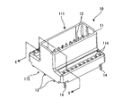
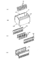
相手コネクタと組み合ったときに相手コネクタのコンタクトと接触する第1のコンタクトが配備され相手コネクタと組み合う嵌合部と、回路基板上に搭載されたときに回路基板に接続される第2のコンタクトが配備され回路基板に搭載される搭載部とを有するハウジングと、
上記第1のコンタクトと上記第2のコンタクトとの双方に直接又は他の回路素子経由で接続され、それら第1のコンタクトと第2のコンタクトを互いに電気的に絶縁するとともに信号を光で中継するフォトカプラを含む電子回路とを備えたことを特徴とする。
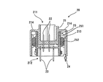
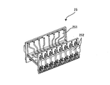
11,21,31,41 ハウジング
12,22 第1のコンタクト
13,23 第2のコンタクト
14,24 半田ペグ
15,25 内蔵回路
100 相手コネクタ
111,211 嵌合部
112,212 搭載部
113,213 回路配置空間
114,214 通気孔
151,251 樹脂成形体
152,252 フォトカプラ
315,415 隔壁
316,317 金属層
318 穴
Claims (4)
- 相手コネクタと組み合ったときに該相手コネクタのコンタクトと接触する第1のコンタクトが配備され該相手コネクタと組み合う嵌合部と、回路基板上に搭載されたときに該回路基板に接続される第2のコンタクトが配備され該回路基板に搭載される搭載部とを有するハウジングと、
前記第1のコンタクトと前記第2のコンタクトとの双方に直接又は他の回路素子経由で接続され、該第1のコンタクトと該第2のコンタクトを互いに電気的に絶縁するとともに信号を光で中継するフォトカプラを含む電子回路とを備え、
前記ハウジングが、前記電子回路が配備された空間を画定する内壁面のうちの一部領域と当該コネクタの外形を画定する外壁面のうちの一部領域との双方を形成する隔壁を有し、該隔壁の、該内壁面上に放熱用の第1の金属層を有するとともに該外壁面上に放熱用の第2の金属層を有し、該第1の金属層と該第2の金属層が互いに金属で繋がっていることを特徴とするコネクタ。 - 相手コネクタと組み合ったときに該相手コネクタのコンタクトと接触する第1のコンタクトが配備され該相手コネクタと組み合う嵌合部と、回路基板上に搭載されたときに該回路基板に接続される第2のコンタクトが配備され該回路基板に搭載される搭載部とを有するハウジングと、
前記第1のコンタクトと前記第2のコンタクトとの双方に直接又は他の回路素子経由で接続され、該第1のコンタクトと該第2のコンタクトを互いに電気的に絶縁するとともに信号を光で中継するフォトカプラを含む電子回路とを備え、
前記ハウジングが、前記電子回路が配備された空間を画定する内壁面のうちの一部領域と当該コネクタの外形を画定する外壁面のうちの一部領域との双方を形成する隔壁を有し、該ハウジングが、相対的に熱伝導率が低い第1の樹脂と相対的に熱伝導率が高い第2の樹脂とからなり、該隔壁が該第2の樹脂で形成されたものであることを特徴とするコネクタ。 - 前記ハウジングが、該ハウジングが回路基板に搭載された状態において当該ハウジング単独で又は該回路基板と共同して前記電子回路を覆う形状を有し、該ハウジングが、該電子回路で発生する熱を、該ハウジングが回路基板に搭載された状態における該回路基板から離れる向きに逃がす放熱用の通気孔を有することを特徴とする請求項1又は2記載のコネクタ。
- 前記フォトカプラが、当該コネクタが回路基板に搭載された状態における該回路基板に対し立設した向きに広がる、搭載面上に搭載されていることを特徴とする請求項1から3のうちいずれか1項記載のコネクタ。
Priority Applications (5)
| Application Number | Priority Date | Filing Date | Title |
|---|---|---|---|
| JP2012164652A JP5872405B2 (ja) | 2012-07-25 | 2012-07-25 | コネクタ |
| KR1020130084730A KR20140013947A (ko) | 2012-07-25 | 2013-07-18 | 커넥터 |
| EP13177907.6A EP2690722A1 (en) | 2012-07-25 | 2013-07-24 | Connector |
| US13/949,716 US20140027656A1 (en) | 2012-07-25 | 2013-07-24 | Connector |
| CN201310315067.XA CN103579864A (zh) | 2012-07-25 | 2013-07-25 | 连接器 |
Applications Claiming Priority (1)
| Application Number | Priority Date | Filing Date | Title |
|---|---|---|---|
| JP2012164652A JP5872405B2 (ja) | 2012-07-25 | 2012-07-25 | コネクタ |
Publications (3)
| Publication Number | Publication Date |
|---|---|
| JP2014026766A JP2014026766A (ja) | 2014-02-06 |
| JP2014026766A5 JP2014026766A5 (ja) | 2015-01-29 |
| JP5872405B2 true JP5872405B2 (ja) | 2016-03-01 |
Family
ID=48832827
Family Applications (1)
| Application Number | Title | Priority Date | Filing Date |
|---|---|---|---|
| JP2012164652A Expired - Fee Related JP5872405B2 (ja) | 2012-07-25 | 2012-07-25 | コネクタ |
Country Status (5)
| Country | Link |
|---|---|
| US (1) | US20140027656A1 (ja) |
| EP (1) | EP2690722A1 (ja) |
| JP (1) | JP5872405B2 (ja) |
| KR (1) | KR20140013947A (ja) |
| CN (1) | CN103579864A (ja) |
Families Citing this family (3)
| Publication number | Priority date | Publication date | Assignee | Title |
|---|---|---|---|---|
| WO2018227575A1 (zh) * | 2017-06-16 | 2018-12-20 | 深圳市得城网络科技有限公司 | 便捷式中继器 |
| US11525709B2 (en) | 2019-04-11 | 2022-12-13 | Veoneer Us, Llc | Electronic unit with vent integrated with terminal aperture |
| JP7140076B2 (ja) * | 2019-08-30 | 2022-09-21 | 株式会社オートネットワーク技術研究所 | コネクタ |
Family Cites Families (21)
| Publication number | Priority date | Publication date | Assignee | Title |
|---|---|---|---|---|
| US4082407A (en) * | 1977-05-20 | 1978-04-04 | Amerace Corporation | Terminal block with encapsulated heat sink |
| JPS57153306A (en) * | 1981-03-17 | 1982-09-21 | Matsushita Electric Works Ltd | Sequence controller |
| JPH0192784U (ja) * | 1987-12-11 | 1989-06-19 | ||
| JPH0319276U (ja) * | 1989-07-04 | 1991-02-26 | ||
| JPH08130077A (ja) * | 1994-10-31 | 1996-05-21 | Matsushita Electric Works Ltd | ランプソケット |
| US6533470B2 (en) * | 2001-03-16 | 2003-03-18 | Infineon Technologies North America Corp. | Single-piece cage for pluggable fiber optic transceiver |
| US20030012363A1 (en) * | 2001-07-16 | 2003-01-16 | Loeb Frederick F. | Jack module with integrated modem interface circuits |
| US20030235375A1 (en) * | 2002-06-25 | 2003-12-25 | Kamath Kishore K. | Transceivers with improved cross talk |
| JP4360859B2 (ja) * | 2003-05-29 | 2009-11-11 | 株式会社日立製作所 | 電子機器 |
| JP4272506B2 (ja) | 2003-12-24 | 2009-06-03 | 京セラ株式会社 | 多数個取り配線基板 |
| WO2005065254A2 (en) * | 2003-12-31 | 2005-07-21 | Fci Americas Technology, Inc. | Electrical power contacts and connectors comprising same |
| JP2005268009A (ja) | 2004-03-18 | 2005-09-29 | Auto Network Gijutsu Kenkyusho:Kk | 制御機能付コネクタ装置 |
| CN101174745B (zh) * | 2006-10-19 | 2012-07-04 | 泰科电子公司 | 包含过压和过电流电路保护的超小型电连接器 |
| US7497737B2 (en) * | 2006-10-19 | 2009-03-03 | Tyco Electronics Corporation | Subminiature electrical connector including over-voltage and over-current circuit protection |
| KR100972979B1 (ko) * | 2008-03-17 | 2010-07-29 | 삼성엘이디 주식회사 | 엘이디 패키지 및 그 제조방법 |
| TWM357044U (en) * | 2008-12-03 | 2009-05-11 | Advanced Connectek Inc | Insulating body and electrical connector therewith |
| CN101872916A (zh) * | 2009-04-24 | 2010-10-27 | 凡甲电子(苏州)有限公司 | 电连接器及其组件 |
| EP2526620B1 (en) * | 2010-01-19 | 2014-01-08 | Johnson Controls Technology Company | Optocoupler circuit for gate driver |
| JP2011249285A (ja) * | 2010-05-31 | 2011-12-08 | Yazaki Corp | Ledユニット |
| US8382509B2 (en) * | 2010-08-06 | 2013-02-26 | Fci Americas Technology Llc | Electrical connector assembly including compliant heat sink |
| US9279946B2 (en) * | 2012-05-23 | 2016-03-08 | Avago Technologies General Ip (Singapore) Pte. Ltd. | Premolded cavity for optoelectronic device |
-
2012
- 2012-07-25 JP JP2012164652A patent/JP5872405B2/ja not_active Expired - Fee Related
-
2013
- 2013-07-18 KR KR1020130084730A patent/KR20140013947A/ko not_active Application Discontinuation
- 2013-07-24 US US13/949,716 patent/US20140027656A1/en not_active Abandoned
- 2013-07-24 EP EP13177907.6A patent/EP2690722A1/en not_active Withdrawn
- 2013-07-25 CN CN201310315067.XA patent/CN103579864A/zh active Pending
Also Published As
| Publication number | Publication date |
|---|---|
| CN103579864A (zh) | 2014-02-12 |
| JP2014026766A (ja) | 2014-02-06 |
| US20140027656A1 (en) | 2014-01-30 |
| KR20140013947A (ko) | 2014-02-05 |
| EP2690722A1 (en) | 2014-01-29 |
Similar Documents
| Publication | Publication Date | Title |
|---|---|---|
| JP4619992B2 (ja) | 電気接続箱 | |
| US10201071B1 (en) | Power supply with thermal insulation function | |
| JP5872405B2 (ja) | コネクタ | |
| JP5930596B2 (ja) | モジュール内蔵コネクタ、及びモジュール内蔵コネクタ付き機器 | |
| WO2016163135A1 (ja) | 電子モジュール及び電子装置 | |
| JP6070977B2 (ja) | 電子回路装置 | |
| JP4851154B2 (ja) | 回路基板内蔵筐体 | |
| JP2007325345A (ja) | 電気接続箱 | |
| JP2009290976A (ja) | 電源分配ボックス | |
| JP2006286757A (ja) | 電子機器の放熱構造 | |
| JP2006304568A (ja) | 電気接続箱 | |
| KR20190055404A (ko) | 방열구조가 구비된 정션블록 | |
| JP2019036674A (ja) | インターポーザ基板およびモジュール部品 | |
| JP2015082593A (ja) | 筐体放熱構造 | |
| JP6551338B2 (ja) | コイル組立体、回路構成体、および、電気接続箱 | |
| JP6630489B2 (ja) | 電子部品ユニット及びワイヤハーネス | |
| JP4676304B2 (ja) | 基板モジュールおよび電気接続箱 | |
| JP2006187122A (ja) | 回路構成体 | |
| JP5370731B2 (ja) | 回路ユニット、回路構成体、電気接続箱および回路ユニットの製造方法 | |
| WO2017098899A1 (ja) | 電気接続箱 | |
| JP6877523B1 (ja) | ヒートシンク、および電子機器ユニット | |
| JP6202436B2 (ja) | 電気機器 | |
| JP2017046509A (ja) | 放熱構造及び電気接続箱 | |
| JP2005252687A (ja) | 携帯端末機器におけるオプション機能部および携帯端末機器 | |
| JP2005142498A (ja) | パワー回路体 |
Legal Events
| Date | Code | Title | Description |
|---|---|---|---|
| A521 | Written amendment |
Free format text: JAPANESE INTERMEDIATE CODE: A523 Effective date: 20141209 |
|
| A621 | Written request for application examination |
Free format text: JAPANESE INTERMEDIATE CODE: A621 Effective date: 20141209 |
|
| A131 | Notification of reasons for refusal |
Free format text: JAPANESE INTERMEDIATE CODE: A131 Effective date: 20150825 |
|
| A521 | Written amendment |
Free format text: JAPANESE INTERMEDIATE CODE: A523 Effective date: 20151002 |
|
| A131 | Notification of reasons for refusal |
Free format text: JAPANESE INTERMEDIATE CODE: A131 Effective date: 20151027 |
|
| A521 | Written amendment |
Free format text: JAPANESE INTERMEDIATE CODE: A523 Effective date: 20151130 |
|
| TRDD | Decision of grant or rejection written | ||
| A01 | Written decision to grant a patent or to grant a registration (utility model) |
Free format text: JAPANESE INTERMEDIATE CODE: A01 Effective date: 20151222 |
|
| A61 | First payment of annual fees (during grant procedure) |
Free format text: JAPANESE INTERMEDIATE CODE: A61 Effective date: 20160113 |
|
| R150 | Certificate of patent or registration of utility model |
Ref document number: 5872405 Country of ref document: JP Free format text: JAPANESE INTERMEDIATE CODE: R150 |
|
| LAPS | Cancellation because of no payment of annual fees |