JP5859212B2 - Manufacturing method of member with recess - Google Patents
Manufacturing method of member with recess Download PDFInfo
- Publication number
- JP5859212B2 JP5859212B2 JP2011028634A JP2011028634A JP5859212B2 JP 5859212 B2 JP5859212 B2 JP 5859212B2 JP 2011028634 A JP2011028634 A JP 2011028634A JP 2011028634 A JP2011028634 A JP 2011028634A JP 5859212 B2 JP5859212 B2 JP 5859212B2
- Authority
- JP
- Japan
- Prior art keywords
- polishing
- angle
- manufacturing
- recesses
- recess
- Prior art date
- Legal status (The legal status is an assumption and is not a legal conclusion. Google has not performed a legal analysis and makes no representation as to the accuracy of the status listed.)
- Active
Links
- 238000004519 manufacturing process Methods 0.000 title claims description 28
- PXHVJJICTQNCMI-UHFFFAOYSA-N Nickel Chemical compound [Ni] PXHVJJICTQNCMI-UHFFFAOYSA-N 0.000 claims description 66
- 238000005498 polishing Methods 0.000 claims description 66
- 239000000463 material Substances 0.000 claims description 44
- RYGMFSIKBFXOCR-UHFFFAOYSA-N Copper Chemical group [Cu] RYGMFSIKBFXOCR-UHFFFAOYSA-N 0.000 claims description 34
- 229910052802 copper Inorganic materials 0.000 claims description 34
- 239000010949 copper Substances 0.000 claims description 34
- 229910052759 nickel Inorganic materials 0.000 claims description 33
- 229910052751 metal Inorganic materials 0.000 claims description 29
- 239000002184 metal Substances 0.000 claims description 29
- 239000000758 substrate Substances 0.000 claims description 19
- 239000011345 viscous material Substances 0.000 claims description 16
- 239000011347 resin Substances 0.000 claims description 14
- 229920005989 resin Polymers 0.000 claims description 14
- 238000000034 method Methods 0.000 claims description 12
- 230000015572 biosynthetic process Effects 0.000 claims description 11
- 229920001971 elastomer Polymers 0.000 claims description 10
- 239000005060 rubber Substances 0.000 claims description 10
- 238000005260 corrosion Methods 0.000 claims description 9
- 230000007797 corrosion Effects 0.000 claims description 9
- 238000000059 patterning Methods 0.000 claims description 9
- 239000011248 coating agent Substances 0.000 claims description 4
- 238000000576 coating method Methods 0.000 claims description 4
- 238000002360 preparation method Methods 0.000 claims 1
- 238000007747 plating Methods 0.000 description 68
- 239000010408 film Substances 0.000 description 38
- 229910052782 aluminium Inorganic materials 0.000 description 12
- XAGFODPZIPBFFR-UHFFFAOYSA-N aluminium Chemical compound [Al] XAGFODPZIPBFFR-UHFFFAOYSA-N 0.000 description 12
- 239000000976 ink Substances 0.000 description 12
- XEEYBQQBJWHFJM-UHFFFAOYSA-N Iron Chemical compound [Fe] XEEYBQQBJWHFJM-UHFFFAOYSA-N 0.000 description 8
- 239000000853 adhesive Substances 0.000 description 8
- 230000001070 adhesive effect Effects 0.000 description 8
- 238000007639 printing Methods 0.000 description 8
- YXFVVABEGXRONW-UHFFFAOYSA-N Toluene Chemical compound CC1=CC=CC=C1 YXFVVABEGXRONW-UHFFFAOYSA-N 0.000 description 6
- 239000010953 base metal Substances 0.000 description 6
- 239000000243 solution Substances 0.000 description 6
- XKRFYHLGVUSROY-UHFFFAOYSA-N Argon Chemical compound [Ar] XKRFYHLGVUSROY-UHFFFAOYSA-N 0.000 description 4
- 229920000049 Carbon (fiber) Polymers 0.000 description 4
- VYZAMTAEIAYCRO-UHFFFAOYSA-N Chromium Chemical compound [Cr] VYZAMTAEIAYCRO-UHFFFAOYSA-N 0.000 description 4
- 239000004917 carbon fiber Substances 0.000 description 4
- 239000002131 composite material Substances 0.000 description 4
- 239000007789 gas Substances 0.000 description 4
- 238000007646 gravure printing Methods 0.000 description 4
- 229910052742 iron Inorganic materials 0.000 description 4
- 238000005259 measurement Methods 0.000 description 4
- VNWKTOKETHGBQD-UHFFFAOYSA-N methane Chemical compound C VNWKTOKETHGBQD-UHFFFAOYSA-N 0.000 description 4
- 239000004793 Polystyrene Substances 0.000 description 3
- BQCADISMDOOEFD-UHFFFAOYSA-N Silver Chemical compound [Ag] BQCADISMDOOEFD-UHFFFAOYSA-N 0.000 description 3
- HEMHJVSKTPXQMS-UHFFFAOYSA-M Sodium hydroxide Chemical compound [OH-].[Na+] HEMHJVSKTPXQMS-UHFFFAOYSA-M 0.000 description 3
- 239000012895 dilution Substances 0.000 description 3
- 238000010790 dilution Methods 0.000 description 3
- 229920002223 polystyrene Polymers 0.000 description 3
- 229920002635 polyurethane Polymers 0.000 description 3
- 239000004814 polyurethane Substances 0.000 description 3
- 229920002379 silicone rubber Polymers 0.000 description 3
- 239000004945 silicone rubber Substances 0.000 description 3
- 229910052709 silver Inorganic materials 0.000 description 3
- 239000004332 silver Substances 0.000 description 3
- 229920003051 synthetic elastomer Polymers 0.000 description 3
- 229920003002 synthetic resin Polymers 0.000 description 3
- 239000000057 synthetic resin Substances 0.000 description 3
- 239000005061 synthetic rubber Substances 0.000 description 3
- OKTJSMMVPCPJKN-UHFFFAOYSA-N Carbon Chemical compound [C] OKTJSMMVPCPJKN-UHFFFAOYSA-N 0.000 description 2
- UFHFLCQGNIYNRP-UHFFFAOYSA-N Hydrogen Chemical compound [H][H] UFHFLCQGNIYNRP-UHFFFAOYSA-N 0.000 description 2
- 229910052786 argon Inorganic materials 0.000 description 2
- 235000013361 beverage Nutrition 0.000 description 2
- 229910052799 carbon Inorganic materials 0.000 description 2
- 238000005229 chemical vapour deposition Methods 0.000 description 2
- 229910052804 chromium Inorganic materials 0.000 description 2
- 239000011651 chromium Substances 0.000 description 2
- ORTQZVOHEJQUHG-UHFFFAOYSA-L copper(II) chloride Chemical compound Cl[Cu]Cl ORTQZVOHEJQUHG-UHFFFAOYSA-L 0.000 description 2
- 239000003814 drug Substances 0.000 description 2
- 238000009820 dry lamination Methods 0.000 description 2
- 235000013305 food Nutrition 0.000 description 2
- 238000000227 grinding Methods 0.000 description 2
- UQEAIHBTYFGYIE-UHFFFAOYSA-N hexamethyldisiloxane Chemical compound C[Si](C)(C)O[Si](C)(C)C UQEAIHBTYFGYIE-UHFFFAOYSA-N 0.000 description 2
- 230000003287 optical effect Effects 0.000 description 2
- 239000005022 packaging material Substances 0.000 description 2
- 238000004544 sputter deposition Methods 0.000 description 2
- 239000011550 stock solution Substances 0.000 description 2
- 239000010409 thin film Substances 0.000 description 2
- XLYOFNOQVPJJNP-UHFFFAOYSA-N water Substances O XLYOFNOQVPJJNP-UHFFFAOYSA-N 0.000 description 2
- 239000000919 ceramic Substances 0.000 description 1
- 229960003280 cupric chloride Drugs 0.000 description 1
- 230000000694 effects Effects 0.000 description 1
- 238000010894 electron beam technology Methods 0.000 description 1
- 238000005530 etching Methods 0.000 description 1
- 238000012986 modification Methods 0.000 description 1
- 230000004048 modification Effects 0.000 description 1
- 239000002985 plastic film Substances 0.000 description 1
- 229920006255 plastic film Polymers 0.000 description 1
- 238000007788 roughening Methods 0.000 description 1
- 238000007790 scraping Methods 0.000 description 1
Images


Classifications
-
- B—PERFORMING OPERATIONS; TRANSPORTING
- B41—PRINTING; LINING MACHINES; TYPEWRITERS; STAMPS
- B41F—PRINTING MACHINES OR PRESSES
- B41F7/00—Rotary lithographic machines
- B41F7/20—Details
-
- B—PERFORMING OPERATIONS; TRANSPORTING
- B41—PRINTING; LINING MACHINES; TYPEWRITERS; STAMPS
- B41N—PRINTING PLATES OR FOILS; MATERIALS FOR SURFACES USED IN PRINTING MACHINES FOR PRINTING, INKING, DAMPING, OR THE LIKE; PREPARING SUCH SURFACES FOR USE AND CONSERVING THEM
- B41N1/00—Printing plates or foils; Materials therefor
- B41N1/04—Printing plates or foils; Materials therefor metallic
- B41N1/06—Printing plates or foils; Materials therefor metallic for relief printing or intaglio printing
-
- B—PERFORMING OPERATIONS; TRANSPORTING
- B41—PRINTING; LINING MACHINES; TYPEWRITERS; STAMPS
- B41N—PRINTING PLATES OR FOILS; MATERIALS FOR SURFACES USED IN PRINTING MACHINES FOR PRINTING, INKING, DAMPING, OR THE LIKE; PREPARING SUCH SURFACES FOR USE AND CONSERVING THEM
- B41N1/00—Printing plates or foils; Materials therefor
- B41N1/12—Printing plates or foils; Materials therefor non-metallic other than stone, e.g. printing plates or foils comprising inorganic materials in an organic matrix
-
- B—PERFORMING OPERATIONS; TRANSPORTING
- B41—PRINTING; LINING MACHINES; TYPEWRITERS; STAMPS
- B41N—PRINTING PLATES OR FOILS; MATERIALS FOR SURFACES USED IN PRINTING MACHINES FOR PRINTING, INKING, DAMPING, OR THE LIKE; PREPARING SUCH SURFACES FOR USE AND CONSERVING THEM
- B41N1/00—Printing plates or foils; Materials therefor
- B41N1/16—Curved printing plates, especially cylinders
- B41N1/20—Curved printing plates, especially cylinders made of metal or similar inorganic compounds, e.g. plasma coated ceramics, carbides
-
- B—PERFORMING OPERATIONS; TRANSPORTING
- B41—PRINTING; LINING MACHINES; TYPEWRITERS; STAMPS
- B41N—PRINTING PLATES OR FOILS; MATERIALS FOR SURFACES USED IN PRINTING MACHINES FOR PRINTING, INKING, DAMPING, OR THE LIKE; PREPARING SUCH SURFACES FOR USE AND CONSERVING THEM
- B41N3/00—Preparing for use and conserving printing surfaces
- B41N3/003—Preparing for use and conserving printing surfaces of intaglio formes, e.g. application of a wear-resistant coating, such as chrome, on the already-engraved plate or cylinder; Preparing for reuse, e.g. removing of the Ballard shell; Correction of the engraving
-
- B—PERFORMING OPERATIONS; TRANSPORTING
- B41—PRINTING; LINING MACHINES; TYPEWRITERS; STAMPS
- B41C—PROCESSES FOR THE MANUFACTURE OR REPRODUCTION OF PRINTING SURFACES
- B41C1/00—Forme preparation
- B41C1/18—Curved printing formes or printing cylinders
-
- B—PERFORMING OPERATIONS; TRANSPORTING
- B41—PRINTING; LINING MACHINES; TYPEWRITERS; STAMPS
- B41N—PRINTING PLATES OR FOILS; MATERIALS FOR SURFACES USED IN PRINTING MACHINES FOR PRINTING, INKING, DAMPING, OR THE LIKE; PREPARING SUCH SURFACES FOR USE AND CONSERVING THEM
- B41N1/00—Printing plates or foils; Materials therefor
- B41N1/02—Printing plates or foils; Materials therefor made of stone
-
- B—PERFORMING OPERATIONS; TRANSPORTING
- B41—PRINTING; LINING MACHINES; TYPEWRITERS; STAMPS
- B41N—PRINTING PLATES OR FOILS; MATERIALS FOR SURFACES USED IN PRINTING MACHINES FOR PRINTING, INKING, DAMPING, OR THE LIKE; PREPARING SUCH SURFACES FOR USE AND CONSERVING THEM
- B41N1/00—Printing plates or foils; Materials therefor
- B41N1/16—Curved printing plates, especially cylinders
- B41N1/18—Curved printing plates, especially cylinders made of stone
Landscapes
- Engineering & Computer Science (AREA)
- Chemical & Material Sciences (AREA)
- Ceramic Engineering (AREA)
- Inorganic Chemistry (AREA)
- Mechanical Engineering (AREA)
- Printing Plates And Materials Therefor (AREA)
- Manufacture Or Reproduction Of Printing Formes (AREA)
- Photosensitive Polymer And Photoresist Processing (AREA)
Description
本発明は、DLC(ダイヤモンドライクカーボン)によって多数の微細な凹部を表面に設けた凹部付き部材の製造方法に関する。 The present invention relates to a method for producing a member with concave portions provided a large number of minute depressions on the surface by DLC (diamond-like carbon).
表面に多数の微細な凹部が形成された画線部と前記凹部の形成されていない非画線部とを有する凹部付き部材として、グラビア製版シリンダーや平凹版がある。グラビア製版シリンダーとしては、例えば特許文献1に示すように、グラビアセルを被覆する硬質皮膜として、DLC(ダイヤモンドライクカーボン)を用いた技術が知られている。 Gravure plate cylinders and plano-concave plates are examples of members with recesses having an image line part having a number of fine recesses formed on the surface and a non-image line part having no recess. As a gravure plate making cylinder, for example, as shown in Patent Document 1, a technique using DLC (diamond-like carbon) as a hard film covering a gravure cell is known.
一方、表面に多数の微細な凹部が形成された画線部と前記凹部の形成されていない非画線部とを有する凹部付き部材として、接着剤、特に食品、飲料、及び医薬品等の包装材料に用いられるドライラミネーション用接着剤を被塗布体に対して均一に塗布することができる塗布シリンダーが知られている。 On the other hand, as a member with a recess having an image line portion having a number of fine recesses formed on the surface and a non-image line portion where the recess is not formed, an adhesive, particularly a packaging material for foods, beverages, pharmaceuticals, etc. 2. Description of the Related Art An application cylinder that can uniformly apply an adhesive for dry lamination used in the method to an object to be applied is known.
また、表面に多数の微細な凹部が形成された画線部と前記凹部の形成されていない非画線部とを有する凹部付き部材として、回路基板、セラミックス電子部品、PDP(プラズマディスプレーパネル)の前面フィルタや電磁波シールド性光透過窓材等の電子部品を製造するにあたり、銀ペースト含有インクといった機能性インク等の導電性ペーストを印刷するにあたって、グラビア製版シリンダーなどが用いられている。 Moreover, as a member with a recessed part which has an image line part in which many fine recessed parts were formed on the surface and a non-image line part in which the recessed part is not formed, a circuit board, a ceramic electronic component, a PDP (plasma display panel) In manufacturing electronic parts such as a front filter and an electromagnetic shielding light transmitting window material, a gravure plate cylinder is used to print a conductive paste such as a functional ink such as a silver paste-containing ink.
これらグラビア製版ロール、平凹版や塗布シリンダーなどの凹部付き部材は、使用時にはその表面にドクターブレードの刃先を水平に当接せしめ、前記表面の余剰なインクや接着剤などの粘性材料を掻き取りながら使用される。 When using these gravure plate rolls, plano-intaglio plates, and application cylinders with concave parts, the blade edge of the doctor blade is in contact with the surface horizontally while scraping off the viscous material such as excess ink and adhesive on the surface. used.
しかしながら、その表面を被覆する硬質皮膜としてDLCを用いた場合、DLCは摩擦係数が低いため、非画線部についたインキをドクターブレードでうまく掻き取れず、いわゆる版かぶりが生ずるという問題があった。 However, when DLC is used as a hard film covering the surface, DLC has a low coefficient of friction, so the ink attached to the non-image area cannot be scraped well with a doctor blade, and there is a problem that so-called plate fogging occurs. .
本発明は、上記した従来技術の問題点に鑑みなされたもので、版かぶりの問題を解消するようにした凹部付き部材の製造方法を提供することを目的とする。 The present invention has been made in view of the problems of the prior art described above, and an object thereof is to provide a method of manufacturing a member with concave portions which is adapted to eliminate the plate fogging problem.
本凹部付き部材は、表面に多数の凹部が形成された画線部と前記凹部の形成されていない非画線部とを有し、粘性材料に前記表面が当接されることで前記凹部に粘性材料が溜められ、前記表面にドクターブレードを水平に突き立てて相対的に移動させることにより、前記表面の余剰な前記粘性材料が掻き取られるようにした凹部付き部材であり、表面に多数の凹部が形成された画線部と前記凹部の形成されていない非画線部とを有するベース部材と、前記画線部及び非画線部を被覆するように形成されてなるDLC被膜とを含み、前記DLC被膜に対して研磨を行うことにより、前記表面にドクターブレードを水平に突き立てた際の仮想延長線に対して0°及び90°以外の斜めの角度をなす複数の研磨痕跡が形成されてなり、前記研磨痕跡が、前記ドクターブレードの仮想延長線に対して0°及び90°以外の斜めの角度をなす第一の角度と、前記ドクターブレードの仮想延長線に対して0°及び90°以外の斜めの角度をなす第二の角度と、を有し、前記第一の角度の研磨痕跡と第二の角度の研磨痕跡とが互いに交差してなることを特徴とする。 The member with concave portions has an image line portion in which a large number of concave portions are formed on a surface and a non-image line portion in which the concave portions are not formed, and the surface is brought into contact with a viscous material to form the concave portion. A viscous material is stored, and a doctor blade is horizontally projected on the surface and moved relatively to thereby scrape off the excessive viscous material on the surface. A base member having an image line portion in which a recess is formed and a non-image line portion in which the recess is not formed, and a DLC film formed so as to cover the image line portion and the non-image line portion. By polishing the DLC film, a plurality of polishing traces are formed at an oblique angle other than 0 ° and 90 ° with respect to a virtual extension line when a doctor blade is horizontally projected on the surface. The polishing trace is A first angle forming an oblique angle other than 0 ° and 90 ° with respect to the virtual extension line of the doctor blade, and an oblique angle other than 0 ° and 90 ° with respect to the virtual extension line of the doctor blade. A polishing angle of the first angle and a polishing mark of the second angle intersecting each other.
DLCは摩擦抵抗が少なく、摺動性が良いため、凹部付き部材表面の柄のないところ(セルのないところ)、すなわち非画線部のインキをうまく掻き取ることができず、版かぶりの問題が生じる。そこで、表面を研磨により粗面化して、摩擦抵抗を上げることで、版かぶりの問題を解消することができる。 Since DLC has low frictional resistance and good slidability, it is difficult to scrape the ink on the surface of the member with a recess (where there is no cell), that is, the non-image area, and the problem of plate fogging Occurs. Therefore, the problem of plate fogging can be solved by roughening the surface by polishing to increase the frictional resistance.
また、前記研磨痕跡が、前記ドクターブレードの仮想延長線に対して0°及び90°以外の斜めの角度をなす第一の角度と、前記ドクターブレードの仮想延長線に対して0°及び90°以外の斜めの角度をなす第二の角度と、を有し、前記第一の角度の研磨痕跡と第二の角度の研磨痕跡とが互いに交差してなるのが好適である。 The polishing trace has a first angle that forms an oblique angle other than 0 ° and 90 ° with respect to the virtual extension line of the doctor blade, and 0 ° and 90 ° with respect to the virtual extension line of the doctor blade. It is preferable that the polishing angle of the first angle and the polishing mark of the second angle intersect each other.
前記研磨痕跡の痕跡深度が0.05μm以上0.3μm未満であるのが好ましい。また、前記研磨はペーパー研磨が好ましく、例えば#1000〜3000程度の番手で研磨を行うのが好ましい。 It is preferable that a trace depth of the polishing trace is 0.05 μm or more and less than 0.3 μm. The polishing is preferably paper polishing, for example, it is preferable to perform polishing with a count of about # 1000 to 3000.
前記凹部付き部材の非画線部の表面の算術平均粗さSaが0.005〜0.10μmであるのが好適である。ここで、算術平均粗さSaは、二次元の算術平均粗さRaを三次元に拡張したものであり、表面形状曲面と平均面で囲まれた部分の体積を測定面積で割ったものである。平均面をxy面、縦方向をz軸とし、測定された表面形状曲線をz=f(x,y)とするとき、算術平均粗さSaは、以下の式で定義される。 It is preferable that the arithmetic average roughness Sa of the surface of the non-imaged portion of the member with concave portions is 0.005 to 0.10 μm. Here, the arithmetic average roughness Sa is a three-dimensional extension of the two-dimensional arithmetic average roughness Ra, and is obtained by dividing the volume surrounded by the surface shape curved surface and the average surface by the measurement area. . When the average plane is the xy plane, the vertical direction is the z-axis, and the measured surface shape curve is z = f (x, y), the arithmetic average roughness Sa is defined by the following equation.

式(数1)において、Lxは、x方向の測定長であり、Lyは、y方向の測定長である。これらはレーザーや電子線による非接触表面形状測定により求められる。
In the equation (Equation 1), Lx is the measurement length in the x direction, and Ly is the measurement length in the y direction. These are obtained by non-contact surface shape measurement using a laser or an electron beam.
前記表面にドクターブレードを水平に突き立てた際の仮想延長線に対する研磨痕跡の斜めの角度としては、10°〜80°が好ましく、30°〜60°がさらに好ましい。 The oblique angle of the polishing trace with respect to the virtual extension line when the doctor blade is horizontally projected on the surface is preferably 10 ° to 80 °, more preferably 30 ° to 60 °.
前記凹部の深度が1μm〜50μmであるのが好適であるが、5〜15μmであるのがより好ましく、5〜10μmがさらに好ましい。凹部に供給するインキ、接着剤や機能性材料などの量が少なくて済むからである。 The depth of the recess is preferably 1 μm to 50 μm, more preferably 5 to 15 μm, and even more preferably 5 to 10 μm. This is because the amount of ink, adhesive, functional material, etc. supplied to the recesses can be small.
前記ベース部材の第一の態様としては、円筒形又は平板状基材と、前記円筒形又は平板状基材の表面に設けられかつ表面に多数の凹部が形成された金属層と、を含むベース部材が好ましい。前記ベース部材の第一の態様では、前記凹部は腐食処理によって形成されるのが好適であり、前記基材としては、アルミ、鉄、又は炭素繊維強化樹脂などの複合材料が好ましい。また、前記ベース部材の第一の態様では、前記金属層としては、銅及び/又はニッケルが好ましい。特に、基材の表面に銅メッキをし、前記銅メッキの上に感光材を塗布し、露光・現像した後、前記銅メッキを腐食せしめて凹部を形成し、その表面にニッケルメッキ又はクロムメッキ等の下地金属メッキ層を施し、ベース部材とするのが好適である。 As a first aspect of the base member, a base including a cylindrical or flat substrate, and a metal layer provided on the surface of the cylindrical or flat substrate and having a plurality of recesses formed on the surface. A member is preferred. In the first aspect of the base member, the recess is preferably formed by a corrosion treatment, and the base material is preferably a composite material such as aluminum, iron, or carbon fiber reinforced resin. In the first aspect of the base member, the metal layer is preferably copper and / or nickel. In particular, copper plating is applied to the surface of the base material, a photosensitive material is applied on the copper plating, exposed and developed, then the copper plating is corroded to form a recess, and nickel plating or chrome plating is applied to the surface. It is preferable to apply a base metal plating layer such as a base member.
前記ベース部材の第二の態様としては、円筒形又は平板状基材と、前記円筒形又は平板状基材の表面に設けられた金属層と、前記金属層上に設けられた感光材を露光・現像してなるパターニング層と、を含むベース部材が好ましい。前記ベース部材の第二の態様では、前記凹部は腐食処理によって形成されるものではなく、前記金属層上に設けられた感光材のパターニングによって実現されるものである。前記基材としては、アルミ、鉄、又は炭素繊維強化樹脂などの複合材料が好ましい。また、前記ベース部材の第二の態様では、前記金属層としては、銅及び/又はニッケルが好ましい。特に、基材の表面に銅メッキをし、前記銅メッキの上にニッケルメッキを施し、前記ニッケルメッキの上に感光材を塗布し、露光・現像することで凹部が前記ニッケルメッキ上に形成される。 As a second aspect of the base member, a cylindrical or flat base material, a metal layer provided on the surface of the cylindrical or flat base material, and a photosensitive material provided on the metal layer are exposed. A base member including a patterning layer formed by development is preferable. In the second aspect of the base member, the recess is not formed by a corrosion treatment, but is realized by patterning a photosensitive material provided on the metal layer. The base material is preferably a composite material such as aluminum, iron, or carbon fiber reinforced resin. In the second aspect of the base member, the metal layer is preferably copper and / or nickel. In particular, copper is plated on the surface of the base material, nickel plating is applied on the copper plating, a photosensitive material is applied on the nickel plating, and a recess is formed on the nickel plating by exposure and development. The
前記基材が、ゴム又はクッション性を有する樹脂からなるクッション層を備えるのがさらに好ましい。すなわち、ゴム又はクッション性を有する樹脂からなるクッション層の上に基材を形成するようにしてもよい。前記クッション層としては、シリコンゴム等の合成ゴムやポリウレタン、ポリスチレン等の弾力性のある合成樹脂を使用することができる。このクッション層の厚さはクッション性即ち弾力性を付与できる厚さであればよく、特別の限定はないが、例えば、1cm〜5cm程度の厚さがあれば充分である。ゴム又はクッション性を有する樹脂からなるクッション層を備えた基材の例としては、例えば特許文献2に記載されたグラビア版などがある。 More preferably, the base material includes a cushion layer made of rubber or a resin having cushioning properties. That is, you may make it form a base material on the cushion layer which consists of resin which has rubber | gum or cushioning properties. As the cushion layer, a synthetic rubber such as silicone rubber, or a synthetic resin having elasticity such as polyurethane or polystyrene can be used. The thickness of the cushion layer is not particularly limited as long as it can provide cushioning properties, that is, elasticity. For example, a thickness of about 1 cm to 5 cm is sufficient. As an example of a base material provided with a cushion layer made of rubber or a resin having cushioning properties, there is a gravure plate described in Patent Document 2, for example.
前記DLC被膜の厚さが、0.1μm〜数10μmであるのが好ましい。より具体的には、0.1μm〜20μmが好ましく、0.1μm〜5μmがさらに好ましい。DLC被膜の形成にあたっては、CVD法又はスパッタ法で薄膜形成するのが好ましい。 The thickness of the DLC film is preferably 0.1 μm to several tens of μm. More specifically, 0.1 μm to 20 μm is preferable, and 0.1 μm to 5 μm is more preferable. In forming the DLC film, it is preferable to form a thin film by CVD or sputtering.
前記凹部付き部材がグラビア製版シリンダーであるのが好ましい。版かぶりの問題が解消され、印刷適性が上がって印刷し易くなるからである。本発明にかかる凹部付き部材であるグラビア製版シリンダーは、パッケージ印刷に好適に用いられるほか、電子部品を製造するにあたり、銀ペースト含有インク等の機能性インクを印刷等する場合にも好適に用いられることができる。 The concave member is preferably a gravure plate cylinder. This is because the problem of plate fog is solved, the printability is improved, and printing becomes easier. The gravure plate cylinder which is a member with a recess according to the present invention is suitably used for package printing, and also suitable for printing functional inks such as silver paste-containing inks in producing electronic components. be able to.
前記凹部付き部材が平凹版であるのが好ましい。版かぶりの問題が解消され、印刷適性が上がって印刷し易くなるからである。 It is preferable that the member with concave portions is a plano-concave plate. This is because the problem of plate fog is solved, the printability is improved, and printing becomes easier.
前記凹部付き部材が塗布シリンダーであるのが好適である。塗布シリンダーとしては、接着剤、特に食品、飲料、及び医薬品等の包装材料に用いられるドライラミネーション用接着剤を被塗布体に対して均一に塗布するための塗布シリンダーなどに好適に用いられる。 It is preferable that the concave member is an application cylinder. The application cylinder is suitably used as an application cylinder for uniformly applying an adhesive, particularly an adhesive for dry lamination used for packaging materials such as foods, beverages, and pharmaceuticals, to an object to be applied.
本製品は、前記凹部付き部材を用いて製造されたことを特徴とする。 This product is manufactured using the member with a recess.
本発明の凹部付き部材の製造方法は、表面に多数の凹部が形成された画線部と前記凹部の形成されていない非画線部とを有し、粘性材料に前記表面が当接されることで前記凹部に粘性材料が溜められ、前記表面にドクターブレードを水平に突き立てて相対的に移動させることにより、前記表面の余剰な前記粘性材料が掻き取られるようにした凹部付き部材の製造方法であり、表面に多数の凹部が形成された画線部と前記凹部の形成されていない非画線部とを有するベース部材を作製するベース部材作製工程と、前記画線部及び非画線部を被覆するようにDLC被膜を形成する被膜形成工程と、前記DLC被膜に対して研磨
を行うことにより、前記表面にドクターブレードを水平に突き立てた際の仮想延長線に対して0°及び90°以外の斜めの角度をなす複数の研磨痕跡を形成する研磨痕跡形成工程と、を含み、前記研磨痕跡形成工程が、前記ドクターブレードの仮想延長線に対して0°及び90°以外の斜めの角度をなす第一の角度と、前記ドクターブレードの仮想延長線に対して0°及び90°以外の斜めの角度をなす第二の角度と、を有し、前記第一の角度の研磨痕跡と第二の角度の研磨痕跡とが互いに交差するように研磨痕跡を形成することを特徴とする。
The manufacturing method of the member with a recessed part of the present invention has an image line part in which a large number of recessed parts are formed on the surface and a non-image line part in which the recessed part is not formed, and the surface is brought into contact with the viscous material. Manufacturing of a member with a recess in which the viscous material is accumulated in the recess, and a doctor blade is protruded horizontally on the surface and moved relatively to scrape off the excess viscous material on the surface. A base member manufacturing step for manufacturing a base member having an image line portion having a large number of recesses formed on a surface thereof and a non-image line portion not formed with the recesses, and the image line portion and the non-image line A film forming step of forming a DLC film so as to cover the portion, and polishing the DLC film, so that the virtual extension line when the doctor blade is horizontally projected on the surface is 0 ° and Diagonal other than 90 ° A polishing trace forming step of forming a plurality of abrasive traces angled, only it contains the polishing trace forming step, first forms an oblique angle other than 0 ° and 90 ° with respect to the virtual extension line of the doctor blade And a second angle that forms an oblique angle other than 0 ° and 90 ° with respect to the virtual extension line of the doctor blade, and the polishing trace of the first angle and the second angle The polishing traces are formed so that the polishing traces intersect each other .
また、前記研磨痕跡形成工程が、前記ドクターブレードの仮想延長線に対して0°及び90°以外の斜めの角度をなす第一の角度と、前記ドクターブレードの仮想延長線に対して0°及び90°以外の斜めの角度をなす第二の角度と、を有し、前記第一の角度の研磨痕跡と第二の角度の研磨痕跡とが互いに交差するように研磨痕跡を形成するのが好適である。 The polishing trace forming step includes a first angle that forms an oblique angle other than 0 ° and 90 ° with respect to the virtual extension line of the doctor blade, and 0 ° with respect to the virtual extension line of the doctor blade. A second angle that forms an oblique angle other than 90 °, and the polishing trace is preferably formed so that the polishing trace of the first angle and the polishing trace of the second angle intersect each other. It is.
前記研磨痕跡の痕跡深度が0.05μm〜0.3μmであるのが好ましい。また、前記研磨はペーパー研磨が好ましく、例えば#1000〜3000程度の番手で研磨を行うのが好ましい。 The trace depth of the polishing trace is preferably 0.05 μm to 0.3 μm. The polishing is preferably paper polishing, for example, it is preferable to perform polishing with a count of about # 1000 to 3000.
前記凹部付き部材の非画線部の表面の算術平均粗さSaが0.005〜0.10μmであるのが好ましい。 It is preferable that the arithmetic average roughness Sa of the surface of the non-image portion of the member with concave portions is 0.005 to 0.10 μm.
前記凹部の深度が1μm〜50μmであるのが好適であるが、5〜15μmであるのがより好ましく、5〜10μmがさらに好ましい。凹部に供給するインキ、接着剤や機能性材料などの量が少なくて済むからである。 The depth of the recess is preferably 1 μm to 50 μm, more preferably 5 to 15 μm, and even more preferably 5 to 10 μm. This is because the amount of ink, adhesive, functional material, etc. supplied to the recesses can be small.
前記ベース部材作製工程の第一の態様としては、円筒形又は平板状基材を準備する工程と、前記円筒形又は平板状基材の表面に金属層を設ける工程と、前記金属層の表面に腐食により多数の凹部を形成させる工程と、を含むのが好適である。前記ベース部材作製工程の第一の態様では、前記凹部は腐食処理によって形成されるのが好適であり、前記基材としては、アルミ、鉄、又は炭素繊維強化樹脂などの複合材料が好ましい。また、前記ベース部材作製工程の第一の態様では、前記金属層としては、銅及び/又はニッケルが好ましい。特に、基材の表面に銅メッキをし、前記銅メッキの上に感光材を塗布し、露光・現像した後、前記銅メッキを腐食せしめて凹部を形成し、その表面にニッケルメッキ又はクロムメッキ等の下地金属メッキ層を施し、ベース部材とするのが好適である。 As a first aspect of the base member manufacturing step, a step of preparing a cylindrical or flat substrate, a step of providing a metal layer on the surface of the cylindrical or flat substrate, and a surface of the metal layer And forming a large number of recesses by corrosion. In the first aspect of the base member manufacturing step, the concave portion is preferably formed by a corrosion treatment, and the base material is preferably a composite material such as aluminum, iron, or carbon fiber reinforced resin. In the first aspect of the base member manufacturing step, the metal layer is preferably copper and / or nickel. In particular, copper plating is applied to the surface of the base material, a photosensitive material is applied on the copper plating, exposed and developed, then the copper plating is corroded to form a recess, and nickel plating or chrome plating is applied to the surface. It is preferable to apply a base metal plating layer such as a base member.
前記ベース部材作製工程の第二の態様としては、円筒形又は平板状基材を準備する工程と、前記円筒形又は平板状基材の表面に金属層を設ける工程と、前記金属層上に設けられた感光材を露光・現像しパターニング層を形成する工程と、を含むのが好ましい。前記ベース部材作製工程の第二の態様では、前記凹部は腐食処理によって形成されるものではなく、前記金属層上に設けられた感光材のパターニングによって実現されるものである。前記基材としては、アルミ、鉄、又は炭素繊維強化樹脂などの複合材料が好ましい。また、前記ベース部材作製工程の第二の態様では、前記金属層としては、銅及び/又はニッケルが好ましい。特に、基材の表面に銅メッキをし、前記銅メッキの上にニッケルメッキを施し、前記ニッケルメッキの上に感光材を塗布し、露光・現像することで凹部が前記ニッケルメッキ上に形成される。 As a second aspect of the base member manufacturing step, a step of preparing a cylindrical or flat substrate, a step of providing a metal layer on the surface of the cylindrical or flat substrate, and a step provided on the metal layer And a step of exposing and developing the obtained photosensitive material to form a patterning layer. In the second aspect of the base member manufacturing step, the recess is not formed by a corrosion process, but is realized by patterning a photosensitive material provided on the metal layer. The base material is preferably a composite material such as aluminum, iron, or carbon fiber reinforced resin. In the second aspect of the base member manufacturing step, the metal layer is preferably copper and / or nickel. In particular, copper is plated on the surface of the base material, nickel plating is applied on the copper plating, a photosensitive material is applied on the nickel plating, and a recess is formed on the nickel plating by exposure and development. The
前記基材が、ゴム又はクッション性を有する樹脂からなるクッション層を備えるのがさらに好ましい。すなわち、ゴム又はクッション性を有する樹脂からなるクッション層の上に基材を形成するようにしてもよい。前記クッション層としては、シリコンゴム等の合成ゴムやポリウレタン、ポリスチレン等の弾力性のある合成樹脂を使用することができる。このクッション層の厚さはクッション性即ち弾力性を付与できる厚さであればよく、特別の限定はないが、例えば、1cm〜5cm程度の厚さがあれば充分である。ゴム又はクッション性を有する樹脂からなるクッション層を備えた基材の例としては、例えば特許文献2に記載されたグラビア版などがある。 More preferably, the base material includes a cushion layer made of rubber or a resin having cushioning properties. That is, you may make it form a base material on the cushion layer which consists of resin which has rubber | gum or cushioning properties. As the cushion layer, a synthetic rubber such as silicone rubber, or a synthetic resin having elasticity such as polyurethane or polystyrene can be used. The thickness of the cushion layer is not particularly limited as long as it can provide cushioning properties, that is, elasticity. For example, a thickness of about 1 cm to 5 cm is sufficient. As an example of a base material provided with a cushion layer made of rubber or a resin having cushioning properties, there is a gravure plate described in Patent Document 2, for example.
前記DLC被膜の厚さが、0.1μm〜数10μmであるのが好ましい。より具体的には、0.1μm〜20μmが好ましく、0.1μm〜5μmがさらに好ましい。DLC被膜の形成にあたっては、CVD法又はスパッタ法で薄膜形成するのが好ましい。 The thickness of the DLC film is preferably 0.1 μm to several tens of μm. More specifically, 0.1 μm to 20 μm is preferable, and 0.1 μm to 5 μm is more preferable. In forming the DLC film, it is preferable to form a thin film by CVD or sputtering.
本発明によれば、版かぶりの問題を解消するようにした凹部付き部材の製造方法を提供することができるという著大な効果を有する。 ADVANTAGE OF THE INVENTION According to this invention, it has the remarkable effect that the manufacturing method of the member with a recessed part which was made to eliminate the problem of plate fogging can be provided.
以下に本発明の実施の形態を説明するが、これら実施の形態は例示的に示されるもので、本発明の技術思想から逸脱しない限り種々の変形が可能なことはいうまでもない。 Embodiments of the present invention will be described below, but these embodiments are exemplarily shown, and it goes without saying that various modifications can be made without departing from the technical idea of the present invention.
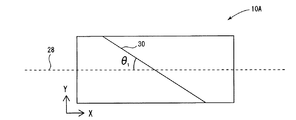
図において、符号10Aは本発明の凹部付き部材を示す。図において、凹部付き部材10Aは、グラビア印刷を行うためのグラビア製版シリンダーの例を示した(図1)。
In the figure,
図1〜図5に基づき説明すると、凹部付き部材10Aは、表面12に多数の凹部14(グラビア製版シリンダーではグラビアセル)が形成された画線部16と、前記凹部14の形成されていない非画線部18、すなわち、凹部14がない平滑な面領域を有している(図1)。そして、粘性材料20(図示例ではインキ)に前記表面12が当接されることで前記凹部14に粘性材料20が溜められ、前記表面12にドクターブレード22を水平に突き立てて相対的に移動(図4の例では、グラビア製版シリンダーである凹部付き部材10Aが回転している)させることにより、前記表面12の余剰な前記粘性材料20が掻き取られるようにした凹部付き部材である。そして、凹部付き部材10Aは、表面12に多数の凹部14が形成された画線部16と前記凹部14の形成されていない非画線部18とを有するベース部材24Aと、前記画線部16と非画線部18を被覆するように形成されてなるDLC被膜26とを含み、前記DLC被膜26に対して研磨を行うことにより、前記表面12にドクターブレード22を水平に突き立てた際の仮想延長線28に対して0°及び90°以外の斜めの角度をなす複数の研磨痕跡30,32が形成されてなるように構成されている。
Referring to FIGS. 1 to 5, the member with recess 10 </ b> A includes an
なお、図4において、符号48は圧胴、50は紙やプラスチックフィルムなどの印刷対象物である。
In FIG. 4,
前記表面12にドクターブレード22を水平に突き立てた際の仮想延長線28とは、凹部付き部材10Aの版面に対して図2、図3に示すようにX軸,Y軸をとった際のX軸方向(横幅方向)と平行な線である。したがって、版面のX軸方向に平行な線を基準として、0°及び90°以外の斜めの角度をなす複数の研磨痕跡30,32が形成されている。
The
前記研磨痕跡30、32は、図2に示すように、前記ドクターブレード22の仮想延長線28に対して0°及び90°以外の斜めの角度をなす第1の角度θ1(図2及び図3の例では30°)だけでもよいが、前記ドクターブレード22の仮想延長線28に対して0°及び90°以外の斜めの角度をなす第2の角度θ2(図2及び図3の例では30°)と、を有し、前記第1の角度θ1の研磨痕跡30と第2の角度θ2の研磨痕跡32とが互いに交差してなるようにするのが好適である。図1では、このように交差させた例を示した。
As shown in FIG. 2, the polishing traces 30 and 32 have a first angle θ 1 that forms an oblique angle other than 0 ° and 90 ° with respect to the
凹部付き部材10Aの製造にあたっては、表面12に多数の凹部14が形成された画線部16と前記凹部14の形成されていない非画線部18とを有するベース部材24Aを作製し、前記画線部16及び非画線部18を被覆するようにDLC被膜26を形成し、前記DLC被膜26に対して研磨を行うことにより、前記表面にドクターブレード22を水平に突き立てた際の仮想延長線28に対して0°及び90°以外の斜めの角度をなす複数の研磨痕跡30、32を形成するようにすればよい。
In manufacturing the member with
また、DLC被膜を設けるベース部材としては、例えば図5又は図6にかかる構成とすることができる。 Moreover, as a base member which provides a DLC film, it can be set as the structure concerning FIG. 5 or FIG. 6, for example.
図5において、前記ベース部材24Aは、円筒形又は平板状基材34と、前記円筒形又は平板状基材34(図示例では円筒形アルミロール)の表面に設けられかつ表面に多数の凹部が形成された金属層36(図示例では銅メッキ)と、を含むベース部材である。前記金属層36はその上にさらにニッケルメッキ層38が設けられた構成とされている。そして、その上にDLC被膜26が形成され、凹部付き部材10Aとされている。なお、図示例では下地金属層としてニッケルメッキ層38を形成した例を示したが、下地金属層としてクロムメッキを用いてもよい。
In FIG. 5, the
前記ベース部材24Aの作製にあたっては、円筒形又は平板状基材34(図示例では円筒形アルミロール)を準備し、前記円筒形又は平板状基材34の表面に金属層36(図示例では銅メッキ)を設け、前記金属層36の表面に感光材を塗布し、露光・現像した後、腐食により前記金属層36の表面に多数の凹部を形成させ、ニッケルメッキを行いニッケルメッキ層38を形成し、ベース部材24Aが作製される。なお、図示例では下地金属層としてニッケルメッキ層38を形成した例を示したが、下地金属層としてクロムメッキを用いてもよい。
In producing the
また、図6に示したベース部材24Bは、円筒形又は平板状基材34と、前記円筒形又は平板状基材34(図示例では円筒形アルミロール)の表面に設けられた金属層40(図示例では銅メッキ層42及びニッケルメッキ層44)と、前記金属層40上に設けられた感光材を露光・現像してなるパターニング層46と、を含むベース部材である。そして、その上にDLC被膜26が形成され、凹部付き部材10Bとされている。
Further, the
前記ベース部材24Bでは、前記凹部14は腐食処理によって形成されるものではなく、前記金属層40上に設けられた感光材のパターニングによって実現されるものである。
In the
前記ベース部材24Bの作製にあたっては、円筒形又は平板状基材34(図示例では円筒形アルミロール)を準備し、前記円筒形又は平板状基材34の表面に金属層40(図示例では銅メッキ層42及びニッケルメッキ層44)を設け、前記金属層40上に感光材を塗布し、露光・現像しパターニング層46を形成し、ベース部材24Bが作製される。
In producing the
なお、前記ベース部材24A及びベース部材24Bにおいて、前記円筒形又は平板状基材34が、ゴム又はクッション性を有する樹脂からなるクッション層を備える構成とすることもできる。すなわち、ゴム又はクッション性を有する樹脂からなるクッション層の上に基材を形成するようにしてもよい。前記クッション層としては、シリコンゴム等の合成ゴムやポリウレタン、ポリスチレン等の弾力性のある合成樹脂を使用することができる。このクッション層の厚さはクッション性即ち弾力性を付与できる厚さであればよく、特別の限定はないが、例えば、1cm〜5cm程度の厚さがあれば充分である。ゴム又はクッション性を有する樹脂からなるクッション層を備えた基材の例としては、例えば特許文献2に記載されたグラビア版などがある。
In addition, in the said
また、上記は、凹部付き部材10A及び凹部付き部材10Bがグラビア製版シリンダーである場合について説明したが、平凹版の場合には平板状基材を用いればよい。また、粘性材料は機能性インク等の機能性材料でもよい。また、塗布シリンダーの場合には、粘性材料が接着剤などとなる。すなわち、ドクターブレードを使う版であれば、本発明の凹部付き部材に含まれる。
Moreover, although the above demonstrated the case where the
以下に実施例をあげて本発明をさらに具体的に説明するが、これらの実施例は例示的に示されるもので限定的に解釈されるべきでないことはいうまでもない。 The present invention will be described more specifically with reference to the following examples. However, it is needless to say that these examples are shown by way of illustration and should not be construed in a limited manner.
(実施例1)
円周600mm、面長1100mmの版母材(アルミ中空ロール)を準備し、ブーメランライン(株式会社シンク・ラボラトリー製全自動レーザーグラビア製版ロール製造装置)を用いて下記する銅メッキ層及びニッケルメッキ層の形成までを行った。まず、版母材(アルミ中空ロール)を銅メッキ槽に装着し、中空ロールをメッキ液に全没させて20A/dm2、6.0Vで80μmの銅メッキ層を形成した。メッキ表面はブツやピットの発生がなく、均一な銅メッキ層を得た。この銅メッキ層の表面を4ヘッド型研磨機(株式会社シンク・ラボラトリー製研磨機)を用いて研磨して当該銅メッキ層の表面を均一な研磨面とした。次いで、上記形成した銅メッキ層を基材としてその表面に感光膜(サーマルレジスト:TSER2104 E4(株式会社シンク・ラボラトリー製))を塗布(ファウンテンコーター)、乾燥した。得られた感光膜の膜厚は膜厚計(FILLMETRICS社製F20、松下テクノトレーデイング社販売)で計ったところ、4μmであった。ついで、画像をレーザー露光し現像した。上記レーザー露光は、Laser Stream FXを用い露光条件500mJ/cm2で所定のパターン露光を行った。また、上記現像は、TLD現像液(株式会社シンク・ラボラトリー製現像液)を用い、現像液希釈比率(原液1:水7)で、24℃90秒間行い、所定のレジストパターンを形成した。次いで、上記形成したレジストパターンをエッチングマスクとして、銅面を腐食した。腐食液には塩化第二銅液を用い、35℃100秒間スプレーにて行いた。また、腐食深度は15μmであった。次いで、水酸化ナトリウムを用い、希釈比率20g/Lで40℃180秒間行い、レジスト剥離を行った。次いで、ニッケルメッキ槽に装着し、メッキ液に半没させて2A/dm2、7.0Vで2μmのニッケルメッキ層を形成した。メッキ表面はブツやピットの発生がなく、均一なニッケルメッキ層を得た。
Example 1
A plate base material (aluminum hollow roll) having a circumference of 600 mm and a surface length of 1100 mm is prepared, and a copper plating layer and a nickel plating layer described below using a boomerang line (a fully automatic laser gravure plate making apparatus manufactured by Sink Laboratory Co., Ltd.) To the formation of. First, a plate base material (aluminum hollow roll) was mounted on a copper plating tank, and the hollow roll was completely immersed in a plating solution to form a copper plating layer of 80 μm at 20 A / dm 2 and 6.0 V. The plating surface was free of bumps and pits, and a uniform copper plating layer was obtained. The surface of the copper plating layer was polished using a 4-head type polishing machine (Sink Laboratory Co., Ltd. polishing machine) to make the surface of the copper plating layer a uniform polishing surface. Next, a photosensitive film (thermal resist: TSER2104 E4 (manufactured by Sink Laboratories)) was applied (fountain coater) on the surface of the formed copper plating layer as a base material and dried. The film thickness of the obtained photosensitive film was 4 μm as measured by a film thickness meter (F20 manufactured by FILLMETRICS, sold by Matsushita Techno Trading). The image was then developed with laser exposure. In the laser exposure, a laser stream FX was used and a predetermined pattern exposure was performed under an exposure condition of 500 mJ / cm 2 . The development was performed at 24 ° C. for 90 seconds at a developer dilution ratio (stock solution 1: water 7) using a TLD developer (Sink Laboratory Co., Ltd. developer) to form a predetermined resist pattern. Next, the copper surface was corroded using the formed resist pattern as an etching mask. A cupric chloride solution was used as the corrosive solution and sprayed at 35 ° C. for 100 seconds. The corrosion depth was 15 μm. Next, using sodium hydroxide, the resist was peeled off at 40 ° C. for 180 seconds at a dilution ratio of 20 g / L. Next, it was mounted in a nickel plating bath and immersed in a plating solution to form a 2 μm nickel plating layer at 2 A / dm 2 and 7.0 V. The plating surface was free of bumps and pits, and a uniform nickel plating layer was obtained.
該ニッケルメッキ層及びレジストパターンの表面にDLC被覆膜をCVD法で形成した。雰囲気アルゴン/水素ガス雰囲気、原料ガスにヘキサメチルジシロキサン、成膜温度80−120℃、成膜時間60分で膜厚0.1μmの中間層を成膜した。次に、原料ガスにトルエン、成膜温度80−120℃、成膜時間90分で膜厚2μmのDLC層を成膜した。 A DLC coating film was formed on the surface of the nickel plating layer and the resist pattern by a CVD method. An intermediate layer having a film thickness of 0.1 μm was formed in an argon / hydrogen gas atmosphere, hexamethyldisiloxane as a source gas, a film formation temperature of 80 to 120 ° C., and a film formation time of 60 minutes. Next, a DLC layer having a thickness of 2 μm was formed as a source gas using toluene, a film formation temperature of 80 to 120 ° C., and a film formation time of 90 minutes.
このようにして得られたシリンダー部材の表面に対し、ペーパー研磨機で番手#2000のペーパー(スリーエム社製)を用い、角度30°で2分間の往復研磨を行い、前記研磨痕跡が、図3に示すように、ドクターブレードの仮想延長線に対して時計回りに30°となる第一の角度を有する研磨痕跡を形成させた。同様にして、前記ドクターブレードの仮想延長線に対して反時計回りに30°となる第二の角度を有する研磨痕跡を形成させ、前記第一の角度の研磨痕跡と第二の角度の研磨痕跡とが互いに交差するようにした。この研磨痕跡を光干渉顕微鏡で観察すると、深度は0.2μmであり、非画線部の表面の算術平均粗さSaが0.03であった。 The surface of the cylinder member thus obtained was subjected to reciprocal polishing for 2 minutes at an angle of 30 ° using a paper of # 2000 paper (manufactured by 3M) with a paper polishing machine. As shown in FIG. 2, a polishing trace having a first angle of 30 ° in the clockwise direction with respect to the virtual extension line of the doctor blade was formed. Similarly, a polishing trace having a second angle of 30 ° counterclockwise with respect to the virtual extension line of the doctor blade is formed, and the polishing trace of the first angle and the polishing trace of the second angle are formed. And crossed each other. When this polishing trace was observed with an optical interference microscope, the depth was 0.2 μm, and the arithmetic average roughness Sa of the surface of the non-image area was 0.03.
このようにして得られた凹部付き部材を用いて、グラビア印刷法により、パッケージ印刷を行った。版かぶりも生ずることなく、きれいなパッケージが得られた。 Package printing was performed by the gravure printing method using the member with a recess thus obtained. A clean package was obtained without plate fogging.
(実施例2)
円周600mm、面長1100mmの版母材(アルミ中空ロール)を準備し、ブーメランライン(株式会社シンク・ラボラトリー製全自動レーザーグラビア製版ロール製造装置)を用いて下記する銅メッキ層及びニッケルメッキ層の形成までを行った。まず、版母材(アルミ中空ロール)を銅メッキ槽に装着し、中空ロールをメッキ液に全没させて20A/dm2、6.0Vで80μmの銅メッキ層を形成した。メッキ表面はブツやピットの発生がなく、均一な銅メッキ層を得た。この銅メッキ層の表面を4ヘッド型研磨機(株式会社シンク・ラボラトリー製研磨機)を用いて研磨して当該銅メッキ層の表面を均一な研磨面とした。次いで、ニッケルメッキ槽に装着し、メッキ液に半没させて2A/dm2、7.0Vで2μmのニッケルメッキ層を形成した。メッキ表面はブツやピットの発生がなく、均一なニッケルメッキ層を得た。上記形成したニッケルメッキ層を基材としてその表面に感光膜(サーマルレジスト:TSER−NS(株式会社シンク・ラボラトリー製))を塗布(ファウンテンコーター)、乾燥した。得られた感光膜の膜厚は膜厚計(FILLMETRICS社製F20、松下テクノトレーデイング社販売)で計ったところ、7μmであった。ついで、画像をレーザー露光し現像した。上記レーザー露光は、Laser Stream FXを用い露光条件300mJ/cm2で所定のパターン露光を行った。また、上記現像は、TLD現像液(株式会社シンク・ラボラトリー製現像液)を用い、現像液希釈比率(原液1:水7)で、24℃90秒間行い、所定のレジストパターンを形成した。
(Example 2)
A plate base material (aluminum hollow roll) having a circumference of 600 mm and a surface length of 1100 mm is prepared, and a copper plating layer and a nickel plating layer described below using a boomerang line (a fully automatic laser gravure plate making apparatus manufactured by Sink Laboratory Co., Ltd.) To the formation of. First, a plate base material (aluminum hollow roll) was mounted on a copper plating tank, and the hollow roll was completely immersed in a plating solution to form a copper plating layer of 80 μm at 20 A / dm 2 and 6.0 V. The plating surface was free of bumps and pits, and a uniform copper plating layer was obtained. The surface of the copper plating layer was polished using a 4-head type polishing machine (Sink Laboratory Co., Ltd. polishing machine) to make the surface of the copper plating layer a uniform polishing surface. Next, it was mounted in a nickel plating bath and immersed in a plating solution to form a 2 μm nickel plating layer at 2 A / dm 2 and 7.0 V. The plating surface was free of bumps and pits, and a uniform nickel plating layer was obtained. Using the formed nickel plating layer as a base material, a photosensitive film (thermal resist: TSER-NS (manufactured by Sink Laboratories)) was applied to the surface (fountain coater) and dried. The film thickness of the obtained photosensitive film was 7 μm as measured by a film thickness meter (F20 manufactured by FILLMETRICS, sold by Matsushita Techno Trading). The image was then developed with laser exposure. In the laser exposure, a laser stream FX was used and a predetermined pattern exposure was performed under an exposure condition of 300 mJ / cm 2 . The development was performed at 24 ° C. for 90 seconds at a developer dilution ratio (stock solution 1: water 7) using a TLD developer (Sink Laboratory Co., Ltd. developer) to form a predetermined resist pattern.
該ニッケルメッキ層及びレジストパターンの表面にDLC被覆膜をCVD法で形成した。雰囲気アルゴン/水素ガス雰囲気、原料ガスにヘキサメチルジシロキサン、成膜温度80−120℃、成膜時間60分で膜厚0.1μmの中間層を成膜した。次に、原料ガスにトルエン、成膜温度80−120℃、成膜時間90分で膜厚2μmのDLC層を成膜した。 A DLC coating film was formed on the surface of the nickel plating layer and the resist pattern by a CVD method. An intermediate layer having a film thickness of 0.1 μm was formed in an argon / hydrogen gas atmosphere, hexamethyldisiloxane as a source gas, a film formation temperature of 80 to 120 ° C., and a film formation time of 60 minutes. Next, a DLC layer having a thickness of 2 μm was formed as a source gas using toluene, a film formation temperature of 80 to 120 ° C., and a film formation time of 90 minutes.
このようにして得られたシリンダー部材の表面に対し、ペーパー研磨機で番手#2000のペーパー(スリーエム社製)を用い、角度30°で2分間の往復研磨を行い、前記研磨痕跡が、図3に示すように、ドクターブレードの仮想延長線に対して時計回りに30°となる第一の角度を有する研磨痕跡を形成させた。同様にして、前記ドクターブレードの仮想延長線に対して反時計回りに30°となる第二の角度を有する研磨痕跡を形成させ、前記第一の角度の研磨痕跡と第二の角度の研磨痕跡とが互いに交差するようにした。この研磨痕跡を光干渉顕微鏡で観察すると、深度は0.2μmであり、非画線部の表面の算術平均粗さSaが0.03であった。 The surface of the cylinder member thus obtained was subjected to reciprocal polishing for 2 minutes at an angle of 30 ° using a paper of # 2000 paper (manufactured by 3M) with a paper polishing machine. As shown in FIG. 2, a polishing trace having a first angle of 30 ° in the clockwise direction with respect to the virtual extension line of the doctor blade was formed. Similarly, a polishing trace having a second angle of 30 ° counterclockwise with respect to the virtual extension line of the doctor blade is formed, and the polishing trace of the first angle and the polishing trace of the second angle are formed. And crossed each other. When this polishing trace was observed with an optical interference microscope, the depth was 0.2 μm, and the arithmetic average roughness Sa of the surface of the non-image area was 0.03.
このようにして得られた凹部付き部材を用いて、グラビア印刷法により、銀ペースト含有インクで電極の配線パターンを印刷した。版かぶりも生ずることなく、きれいな電極の配線パターンが得られた。 A wiring pattern of an electrode was printed with a silver paste-containing ink by a gravure printing method using the member with a recess thus obtained. A clean electrode wiring pattern was obtained without plate fogging.
10A,10B:凹部付き部材、12:表面、14:凹部、16:画線部、18:非画線部、20:粘性材料、22:ドクターブレード、24A,24B:ベース部材、26:DLC被膜、28:仮想延長線、30,32:研磨痕跡、34:円筒形又は平板状基材、36,40:金属層、38:ニッケルメッキ層、42:銅メッキ層、44:ニッケルメッキ層、46:パターニング層、48:圧胴、50:印刷対象物。 10A, 10B: member with recesses, 12: surface, 14: recesses, 16: image area, 18: non-image area, 20: viscous material, 22: doctor blade, 24A, 24B: base member, 26: DLC coating , 28: virtual extension line, 30, 32: polishing trace, 34: cylindrical or flat substrate, 36, 40: metal layer, 38: nickel plating layer, 42: copper plating layer, 44: nickel plating layer, 46 : Patterning layer, 48: impression cylinder, 50: printing object.
Claims (9)
表面に多数の凹部が形成された画線部と前記凹部の形成されていない非画線部とを有するベース部材を作製するベース部材作製工程と、前記画線部及び非画線部を被覆するようにDLC被膜を形成する被膜形成工程と、
前記DLC被膜に対して研磨を行うことにより、前記表面にドクターブレードを水平に突き立てた際の仮想延長線に対して0°及び90°以外の斜めの角度をなす複数の研磨痕跡を形成する研磨痕跡形成工程と、
を含み、
前記研磨痕跡形成工程が、前記ドクターブレードの仮想延長線に対して0°及び90°以外の斜めの角度をなす第一の角度と、前記ドクターブレードの仮想延長線に対して0°及び90°以外の斜めの角度をなす第二の角度と、を有し、前記第一の角度の研磨痕跡と第二の角度の研磨痕跡とが互いに交差するように研磨痕跡を形成することを特徴とする凹部付き部材の製造方法。 It has an image line part in which a large number of recesses are formed on the surface and a non-image line part in which the recesses are not formed, and the viscous material is stored in the recesses by contacting the surface with the viscous material, It is a method of manufacturing a member with a recess that allows a surplus of the viscous material on the surface to be scraped off by horizontally moving a doctor blade on the surface.
A base member manufacturing step of manufacturing a base member having an image line portion having a large number of recesses formed on the surface and a non-image line portion having no recesses, and covering the image line portion and the non-image line portion A film forming step of forming a DLC film,
By polishing the DLC film, a plurality of polishing traces are formed at an angle other than 0 ° and 90 ° with respect to a virtual extension line when a doctor blade is projected horizontally on the surface. Polishing trace formation step;
Including
The polishing trace forming step includes a first angle forming an oblique angle other than 0 ° and 90 ° with respect to the virtual extension line of the doctor blade, and 0 ° and 90 ° with respect to the virtual extension line of the doctor blade. A second angle that forms an oblique angle other than the above, and the polishing trace is formed so that the polishing trace of the first angle and the polishing trace of the second angle intersect each other. Manufacturing method of member with a recess.
Priority Applications (8)
| Application Number | Priority Date | Filing Date | Title |
|---|---|---|---|
| JP2011028634A JP5859212B2 (en) | 2011-02-14 | 2011-02-14 | Manufacturing method of member with recess |
| CN201280005813.9A CN103328226B (en) | 2011-02-14 | 2012-02-14 | Component with recess and manufacture method thereof |
| KR1020137018002A KR101659771B1 (en) | 2011-02-14 | 2012-02-14 | Member with concave portion and method for manufacturing same |
| ES12747273.6T ES2668829T3 (en) | 2011-02-14 | 2012-02-14 | Member with concave piece and method to manufacture the same |
| PCT/JP2012/053315 WO2012111637A1 (en) | 2011-02-14 | 2012-02-14 | Member with concave portion and method for manufacturing same |
| US13/976,658 US9090052B2 (en) | 2011-02-14 | 2012-02-14 | Member with concave portion and method for manufacturing same |
| EP12747273.6A EP2676800B1 (en) | 2011-02-14 | 2012-02-14 | Member with concave portion and method for manufacturing same |
| RU2013128281/12A RU2559127C2 (en) | 2011-02-14 | 2012-02-14 | Printing element with deepened parts and method of its manufacturing |
Applications Claiming Priority (1)
| Application Number | Priority Date | Filing Date | Title |
|---|---|---|---|
| JP2011028634A JP5859212B2 (en) | 2011-02-14 | 2011-02-14 | Manufacturing method of member with recess |
Publications (3)
| Publication Number | Publication Date |
|---|---|
| JP2012166431A JP2012166431A (en) | 2012-09-06 |
| JP2012166431A5 JP2012166431A5 (en) | 2013-12-19 |
| JP5859212B2 true JP5859212B2 (en) | 2016-02-10 |
Family
ID=46672556
Family Applications (1)
| Application Number | Title | Priority Date | Filing Date |
|---|---|---|---|
| JP2011028634A Active JP5859212B2 (en) | 2011-02-14 | 2011-02-14 | Manufacturing method of member with recess |
Country Status (8)
| Country | Link |
|---|---|
| US (1) | US9090052B2 (en) |
| EP (1) | EP2676800B1 (en) |
| JP (1) | JP5859212B2 (en) |
| KR (1) | KR101659771B1 (en) |
| CN (1) | CN103328226B (en) |
| ES (1) | ES2668829T3 (en) |
| RU (1) | RU2559127C2 (en) |
| WO (1) | WO2012111637A1 (en) |
Families Citing this family (6)
| Publication number | Priority date | Publication date | Assignee | Title |
|---|---|---|---|---|
| DE102011002229A1 (en) * | 2011-04-21 | 2012-10-25 | Fercon GmbH | Apparatus and method for the production of gravure and offset printing plates or for printing cylindrical substrates |
| JP6149813B2 (en) * | 2013-10-28 | 2017-06-21 | 株式会社村田製作所 | Gravure plate manufacturing method, gravure printing method, and electronic component manufacturing method |
| CN107206826B (en) * | 2015-02-06 | 2020-09-04 | 株式会社Uacj | Gravure printing roller |
| KR101763166B1 (en) * | 2016-09-22 | 2017-08-03 | 한국과학기술원 | The method of coating a thin film using rolling scheme and the apparatus for coating a thin film using the same |
| CN112808514B (en) * | 2020-12-30 | 2021-11-23 | 珠海冠宇电池股份有限公司 | Gravure roller, gravure coating machine and preparation method of electrode plate |
| CN114228313A (en) * | 2021-11-24 | 2022-03-25 | 张竟夫 | Printing machine roller |
Family Cites Families (20)
| Publication number | Priority date | Publication date | Assignee | Title |
|---|---|---|---|---|
| JPS5824154A (en) * | 1981-08-05 | 1983-02-14 | Fuji Xerox Co Ltd | Transmitting mechanism of rotating force of copying machine |
| JP2635046B2 (en) * | 1987-05-27 | 1997-07-30 | 株式会社 東京機械製作所 | Roller for inking unit of lithographic printing press and method for manufacturing roller for inking unit of lithographic printing press |
| US4862799A (en) * | 1987-11-13 | 1989-09-05 | Rockwell International Corporation | Copper coated anodized aluminum ink metering roller |
| JP3022986B2 (en) * | 1990-10-12 | 2000-03-21 | 大日本印刷株式会社 | Method of preventing printing failure in gravure printing and gravure printing plate |
| JPH07256854A (en) * | 1994-03-18 | 1995-10-09 | Toppan Printing Co Ltd | Flat intaglio requiring no dampening water and method for offset printing using the same |
| JP4117943B2 (en) * | 1998-06-18 | 2008-07-16 | 株式会社シンク・ラボラトリー | Method for producing a printing plate having cushioning properties |
| JP4834944B2 (en) * | 2001-09-13 | 2011-12-14 | 大日本印刷株式会社 | How to prevent printing defects in gravure printing |
| EP1445098A1 (en) * | 2003-02-04 | 2004-08-11 | Kba-Giori S.A. | Blanket cylinder for an intaglio printing machine |
| JP4364534B2 (en) * | 2003-02-19 | 2009-11-18 | ヒラノ技研工業株式会社 | Image forming method |
| CN100446993C (en) * | 2003-05-16 | 2008-12-31 | 富士胶片株式会社 | Method for manufacturing support body for lithographic plate and its support body |
| DE10341709B4 (en) * | 2003-10-08 | 2007-09-20 | Koenig & Bauer Aktiengesellschaft | printing unit |
| CN100451862C (en) * | 2004-12-24 | 2009-01-14 | 东海橡胶工业株式会社 | Developing roll |
| WO2007040141A1 (en) * | 2005-09-30 | 2007-04-12 | Think Laboratory Co., Ltd. | Photogravure engraving roll and production method thereof |
| JP2007130996A (en) | 2005-10-14 | 2007-05-31 | Think Laboratory Co Ltd | Gravure plate-making roll and its manufacturing method |
| CN1986213B (en) * | 2005-12-22 | 2010-12-08 | 鸿富锦精密工业(深圳)有限公司 | Antiwear magnetic coating and its making process |
| US20090301326A1 (en) * | 2005-12-30 | 2009-12-10 | Barr George A | Coated print roll and method therefor |
| WO2007135898A1 (en) * | 2006-05-24 | 2007-11-29 | Think Laboratory Co., Ltd. | Fully automatic manufacturing system for gravure engraving roll |
| JP5198998B2 (en) * | 2007-09-20 | 2013-05-15 | 株式会社シンク・ラボラトリー | Gravure plate having cushioning properties and manufacturing method thereof |
| CN102216487B (en) * | 2008-10-29 | 2014-07-02 | Ntn株式会社 | Hard multilayer film formed body and method for manufacturing same |
| JP5015991B2 (en) * | 2008-11-11 | 2012-09-05 | トーカロ株式会社 | Printing roll and method for producing the same |
-
2011
- 2011-02-14 JP JP2011028634A patent/JP5859212B2/en active Active
-
2012
- 2012-02-14 CN CN201280005813.9A patent/CN103328226B/en active Active
- 2012-02-14 WO PCT/JP2012/053315 patent/WO2012111637A1/en active Application Filing
- 2012-02-14 US US13/976,658 patent/US9090052B2/en active Active
- 2012-02-14 EP EP12747273.6A patent/EP2676800B1/en active Active
- 2012-02-14 KR KR1020137018002A patent/KR101659771B1/en active IP Right Grant
- 2012-02-14 ES ES12747273.6T patent/ES2668829T3/en active Active
- 2012-02-14 RU RU2013128281/12A patent/RU2559127C2/en not_active IP Right Cessation
Also Published As
| Publication number | Publication date |
|---|---|
| EP2676800A4 (en) | 2015-11-25 |
| RU2013128281A (en) | 2015-03-27 |
| US9090052B2 (en) | 2015-07-28 |
| KR20140032968A (en) | 2014-03-17 |
| ES2668829T3 (en) | 2018-05-22 |
| EP2676800B1 (en) | 2018-04-04 |
| WO2012111637A1 (en) | 2012-08-23 |
| KR101659771B1 (en) | 2016-09-26 |
| CN103328226B (en) | 2016-06-08 |
| JP2012166431A (en) | 2012-09-06 |
| RU2559127C2 (en) | 2015-08-10 |
| EP2676800A1 (en) | 2013-12-25 |
| CN103328226A (en) | 2013-09-25 |
| US20130269554A1 (en) | 2013-10-17 |
Similar Documents
| Publication | Publication Date | Title |
|---|---|---|
| JP5859212B2 (en) | Manufacturing method of member with recess | |
| JP3786313B2 (en) | Metal mask manufacturing method | |
| KR20140036130A (en) | Substrate having etching mask and method for producing same | |
| JP6474484B2 (en) | Gravure cylinder and manufacturing method thereof | |
| KR20110003084A (en) | The gravure plate for offset printing and the method of manufacturing the same | |
| JP5327068B2 (en) | Production method of gravure cylinder | |
| JP7465656B2 (en) | Gravure printing plate | |
| KR101648544B1 (en) | Continuous plating patterning roll and manufacturing method therefor | |
| JPH06234202A (en) | Manufacture of mask for screen printing | |
| JP6144907B2 (en) | Method for producing fine metal pattern sheet for sliding surface coating | |
| JPWO2017187626A1 (en) | Blanket for printing, method for producing blanket for printing, and printing method using blanket for printing | |
| JP2000010300A (en) | Production of printing plate having cushion property | |
| JP2014105374A (en) | Stretchable metal mesh and method for manufacturing the same | |
| JPH0516322A (en) | Manufacture of intaglio printing plate | |
| JPH039358A (en) | Gravure pringing plate and production thereof | |
| JPH04267151A (en) | Preparation of planographic printing plate | |
| JP2014081490A (en) | Platemaking roll for gravure printing and method for manufacturing the same | |
| JP2003031923A (en) | Method of forming conductive pattern | |
| TWI647988B (en) | Method of manufacturing touch sensor, rf antenna and high resolution conductive patterns using organometallic ink and banded anilox rolls | |
| JP5768443B2 (en) | Pattern for gravure screen, gravure screen, and gravure version | |
| JP2015128864A (en) | Intaglio plate for gravure offset printing and method for making the plate | |
| JP2003121996A (en) | Method of manufacturing intaglio printing plate | |
| JP2008155614A (en) | Relief printer | |
| TWI294758B (en) | Method for manufacturing flexible printed circuits | |
| JP2009134202A (en) | Method of manufacturing for printing plate |
Legal Events
| Date | Code | Title | Description |
|---|---|---|---|
| A521 | Request for written amendment filed |
Free format text: JAPANESE INTERMEDIATE CODE: A523 Effective date: 20131106 |
|
| A621 | Written request for application examination |
Free format text: JAPANESE INTERMEDIATE CODE: A621 Effective date: 20131106 |
|
| A131 | Notification of reasons for refusal |
Free format text: JAPANESE INTERMEDIATE CODE: A131 Effective date: 20140807 |
|
| A521 | Request for written amendment filed |
Free format text: JAPANESE INTERMEDIATE CODE: A523 Effective date: 20140930 |
|
| A131 | Notification of reasons for refusal |
Free format text: JAPANESE INTERMEDIATE CODE: A131 Effective date: 20150317 |
|
| A521 | Request for written amendment filed |
Free format text: JAPANESE INTERMEDIATE CODE: A523 Effective date: 20150508 |
|
| A131 | Notification of reasons for refusal |
Free format text: JAPANESE INTERMEDIATE CODE: A131 Effective date: 20151016 |
|
| A521 | Request for written amendment filed |
Free format text: JAPANESE INTERMEDIATE CODE: A523 Effective date: 20151113 |
|
| TRDD | Decision of grant or rejection written | ||
| A01 | Written decision to grant a patent or to grant a registration (utility model) |
Free format text: JAPANESE INTERMEDIATE CODE: A01 Effective date: 20151210 |
|
| A61 | First payment of annual fees (during grant procedure) |
Free format text: JAPANESE INTERMEDIATE CODE: A61 Effective date: 20151216 |
|
| R150 | Certificate of patent or registration of utility model |
Ref document number: 5859212 Country of ref document: JP Free format text: JAPANESE INTERMEDIATE CODE: R150 |
|
| R250 | Receipt of annual fees |
Free format text: JAPANESE INTERMEDIATE CODE: R250 |
|
| R250 | Receipt of annual fees |
Free format text: JAPANESE INTERMEDIATE CODE: R250 |
|
| R250 | Receipt of annual fees |
Free format text: JAPANESE INTERMEDIATE CODE: R250 |
|
| R250 | Receipt of annual fees |
Free format text: JAPANESE INTERMEDIATE CODE: R250 |
|
| R250 | Receipt of annual fees |
Free format text: JAPANESE INTERMEDIATE CODE: R250 |
|
| R250 | Receipt of annual fees |
Free format text: JAPANESE INTERMEDIATE CODE: R250 |