JP5850717B2 - Imprint apparatus and article manufacturing method using the same - Google Patents
Imprint apparatus and article manufacturing method using the same Download PDFInfo
- Publication number
- JP5850717B2 JP5850717B2 JP2011255292A JP2011255292A JP5850717B2 JP 5850717 B2 JP5850717 B2 JP 5850717B2 JP 2011255292 A JP2011255292 A JP 2011255292A JP 2011255292 A JP2011255292 A JP 2011255292A JP 5850717 B2 JP5850717 B2 JP 5850717B2
- Authority
- JP
- Japan
- Prior art keywords
- imprint
- inspection
- foreign matter
- moving
- application
- Prior art date
- Legal status (The legal status is an assumption and is not a legal conclusion. Google has not performed a legal analysis and makes no representation as to the accuracy of the status listed.)
- Active
Links
- 238000004519 manufacturing process Methods 0.000 title claims description 12
- 238000007689 inspection Methods 0.000 claims description 140
- 239000011347 resin Substances 0.000 claims description 69
- 229920005989 resin Polymers 0.000 claims description 69
- 238000000576 coating method Methods 0.000 claims description 43
- 239000011248 coating agent Substances 0.000 claims description 41
- 239000000126 substance Substances 0.000 claims description 38
- 239000000758 substrate Substances 0.000 claims description 35
- 230000001133 acceleration Effects 0.000 claims description 6
- 238000009434 installation Methods 0.000 claims description 6
- 238000012545 processing Methods 0.000 claims description 5
- 230000001360 synchronised effect Effects 0.000 claims description 3
- 238000003825 pressing Methods 0.000 claims 3
- 238000000034 method Methods 0.000 description 95
- 230000008569 process Effects 0.000 description 78
- 239000000463 material Substances 0.000 description 12
- 238000010586 diagram Methods 0.000 description 8
- 238000005259 measurement Methods 0.000 description 8
- 238000005286 illumination Methods 0.000 description 7
- 238000001514 detection method Methods 0.000 description 6
- 239000004065 semiconductor Substances 0.000 description 5
- 230000008859 change Effects 0.000 description 4
- 230000007246 mechanism Effects 0.000 description 4
- 239000002245 particle Substances 0.000 description 4
- 230000000694 effects Effects 0.000 description 3
- 238000005530 etching Methods 0.000 description 3
- 238000000016 photochemical curing Methods 0.000 description 3
- KDCGOANMDULRCW-UHFFFAOYSA-N 7H-purine Chemical compound N1=CNC2=NC=NC2=C1 KDCGOANMDULRCW-UHFFFAOYSA-N 0.000 description 2
- 230000001678 irradiating effect Effects 0.000 description 2
- 230000003287 optical effect Effects 0.000 description 2
- 230000002093 peripheral effect Effects 0.000 description 2
- VYPSYNLAJGMNEJ-UHFFFAOYSA-N silicon dioxide Inorganic materials O=[Si]=O VYPSYNLAJGMNEJ-UHFFFAOYSA-N 0.000 description 2
- 230000009471 action Effects 0.000 description 1
- 230000008901 benefit Effects 0.000 description 1
- 230000015572 biosynthetic process Effects 0.000 description 1
- 238000007796 conventional method Methods 0.000 description 1
- 238000012937 correction Methods 0.000 description 1
- 238000001723 curing Methods 0.000 description 1
- 238000005516 engineering process Methods 0.000 description 1
- 239000011521 glass Substances 0.000 description 1
- 238000003384 imaging method Methods 0.000 description 1
- 230000006872 improvement Effects 0.000 description 1
- 239000004973 liquid crystal related substance Substances 0.000 description 1
- 229910021421 monocrystalline silicon Inorganic materials 0.000 description 1
- 238000000465 moulding Methods 0.000 description 1
- 238000000206 photolithography Methods 0.000 description 1
- 239000010453 quartz Substances 0.000 description 1
- 238000012360 testing method Methods 0.000 description 1
- 230000009466 transformation Effects 0.000 description 1
Images


Classifications
-
- G—PHYSICS
- G03—PHOTOGRAPHY; CINEMATOGRAPHY; ANALOGOUS TECHNIQUES USING WAVES OTHER THAN OPTICAL WAVES; ELECTROGRAPHY; HOLOGRAPHY
- G03F—PHOTOMECHANICAL PRODUCTION OF TEXTURED OR PATTERNED SURFACES, e.g. FOR PRINTING, FOR PROCESSING OF SEMICONDUCTOR DEVICES; MATERIALS THEREFOR; ORIGINALS THEREFOR; APPARATUS SPECIALLY ADAPTED THEREFOR
- G03F7/00—Photomechanical, e.g. photolithographic, production of textured or patterned surfaces, e.g. printing surfaces; Materials therefor, e.g. comprising photoresists; Apparatus specially adapted therefor
- G03F7/0002—Lithographic processes using patterning methods other than those involving the exposure to radiation, e.g. by stamping
-
- B—PERFORMING OPERATIONS; TRANSPORTING
- B05—SPRAYING OR ATOMISING IN GENERAL; APPLYING FLUENT MATERIALS TO SURFACES, IN GENERAL
- B05C—APPARATUS FOR APPLYING FLUENT MATERIALS TO SURFACES, IN GENERAL
- B05C11/00—Component parts, details or accessories not specifically provided for in groups B05C1/00 - B05C9/00
- B05C11/10—Storage, supply or control of liquid or other fluent material; Recovery of excess liquid or other fluent material
- B05C11/1002—Means for controlling supply, i.e. flow or pressure, of liquid or other fluent material to the applying apparatus, e.g. valves
- B05C11/1015—Means for controlling supply, i.e. flow or pressure, of liquid or other fluent material to the applying apparatus, e.g. valves responsive to a conditions of ambient medium or target, e.g. humidity, temperature ; responsive to position or movement of the coating head relative to the target
- B05C11/1021—Means for controlling supply, i.e. flow or pressure, of liquid or other fluent material to the applying apparatus, e.g. valves responsive to a conditions of ambient medium or target, e.g. humidity, temperature ; responsive to position or movement of the coating head relative to the target responsive to presence or shape of target
-
- B—PERFORMING OPERATIONS; TRANSPORTING
- B05—SPRAYING OR ATOMISING IN GENERAL; APPLYING FLUENT MATERIALS TO SURFACES, IN GENERAL
- B05C—APPARATUS FOR APPLYING FLUENT MATERIALS TO SURFACES, IN GENERAL
- B05C9/00—Apparatus or plant for applying liquid or other fluent material to surfaces by means not covered by any preceding group, or in which the means of applying the liquid or other fluent material is not important
- B05C9/08—Apparatus or plant for applying liquid or other fluent material to surfaces by means not covered by any preceding group, or in which the means of applying the liquid or other fluent material is not important for applying liquid or other fluent material and performing an auxiliary operation
- B05C9/10—Apparatus or plant for applying liquid or other fluent material to surfaces by means not covered by any preceding group, or in which the means of applying the liquid or other fluent material is not important for applying liquid or other fluent material and performing an auxiliary operation the auxiliary operation being performed before the application
-
- B—PERFORMING OPERATIONS; TRANSPORTING
- B05—SPRAYING OR ATOMISING IN GENERAL; APPLYING FLUENT MATERIALS TO SURFACES, IN GENERAL
- B05C—APPARATUS FOR APPLYING FLUENT MATERIALS TO SURFACES, IN GENERAL
- B05C9/00—Apparatus or plant for applying liquid or other fluent material to surfaces by means not covered by any preceding group, or in which the means of applying the liquid or other fluent material is not important
- B05C9/08—Apparatus or plant for applying liquid or other fluent material to surfaces by means not covered by any preceding group, or in which the means of applying the liquid or other fluent material is not important for applying liquid or other fluent material and performing an auxiliary operation
- B05C9/12—Apparatus or plant for applying liquid or other fluent material to surfaces by means not covered by any preceding group, or in which the means of applying the liquid or other fluent material is not important for applying liquid or other fluent material and performing an auxiliary operation the auxiliary operation being performed after the application
-
- B—PERFORMING OPERATIONS; TRANSPORTING
- B05—SPRAYING OR ATOMISING IN GENERAL; APPLYING FLUENT MATERIALS TO SURFACES, IN GENERAL
- B05D—PROCESSES FOR APPLYING FLUENT MATERIALS TO SURFACES, IN GENERAL
- B05D3/00—Pretreatment of surfaces to which liquids or other fluent materials are to be applied; After-treatment of applied coatings, e.g. intermediate treating of an applied coating preparatory to subsequent applications of liquids or other fluent materials
- B05D3/06—Pretreatment of surfaces to which liquids or other fluent materials are to be applied; After-treatment of applied coatings, e.g. intermediate treating of an applied coating preparatory to subsequent applications of liquids or other fluent materials by exposure to radiation
- B05D3/061—Pretreatment of surfaces to which liquids or other fluent materials are to be applied; After-treatment of applied coatings, e.g. intermediate treating of an applied coating preparatory to subsequent applications of liquids or other fluent materials by exposure to radiation using U.V.
- B05D3/065—After-treatment
- B05D3/067—Curing or cross-linking the coating
-
- B—PERFORMING OPERATIONS; TRANSPORTING
- B05—SPRAYING OR ATOMISING IN GENERAL; APPLYING FLUENT MATERIALS TO SURFACES, IN GENERAL
- B05D—PROCESSES FOR APPLYING FLUENT MATERIALS TO SURFACES, IN GENERAL
- B05D3/00—Pretreatment of surfaces to which liquids or other fluent materials are to be applied; After-treatment of applied coatings, e.g. intermediate treating of an applied coating preparatory to subsequent applications of liquids or other fluent materials
- B05D3/12—Pretreatment of surfaces to which liquids or other fluent materials are to be applied; After-treatment of applied coatings, e.g. intermediate treating of an applied coating preparatory to subsequent applications of liquids or other fluent materials by mechanical means
-
- B—PERFORMING OPERATIONS; TRANSPORTING
- B29—WORKING OF PLASTICS; WORKING OF SUBSTANCES IN A PLASTIC STATE IN GENERAL
- B29C—SHAPING OR JOINING OF PLASTICS; SHAPING OF MATERIAL IN A PLASTIC STATE, NOT OTHERWISE PROVIDED FOR; AFTER-TREATMENT OF THE SHAPED PRODUCTS, e.g. REPAIRING
- B29C59/00—Surface shaping of articles, e.g. embossing; Apparatus therefor
- B29C59/002—Component parts, details or accessories; Auxiliary operations
-
- B—PERFORMING OPERATIONS; TRANSPORTING
- B82—NANOTECHNOLOGY
- B82Y—SPECIFIC USES OR APPLICATIONS OF NANOSTRUCTURES; MEASUREMENT OR ANALYSIS OF NANOSTRUCTURES; MANUFACTURE OR TREATMENT OF NANOSTRUCTURES
- B82Y10/00—Nanotechnology for information processing, storage or transmission, e.g. quantum computing or single electron logic
-
- B—PERFORMING OPERATIONS; TRANSPORTING
- B82—NANOTECHNOLOGY
- B82Y—SPECIFIC USES OR APPLICATIONS OF NANOSTRUCTURES; MEASUREMENT OR ANALYSIS OF NANOSTRUCTURES; MANUFACTURE OR TREATMENT OF NANOSTRUCTURES
- B82Y40/00—Manufacture or treatment of nanostructures
-
- H—ELECTRICITY
- H01—ELECTRIC ELEMENTS
- H01L—SEMICONDUCTOR DEVICES NOT COVERED BY CLASS H10
- H01L21/00—Processes or apparatus adapted for the manufacture or treatment of semiconductor or solid state devices or of parts thereof
- H01L21/02—Manufacture or treatment of semiconductor devices or of parts thereof
- H01L21/04—Manufacture or treatment of semiconductor devices or of parts thereof the devices having potential barriers, e.g. a PN junction, depletion layer or carrier concentration layer
- H01L21/18—Manufacture or treatment of semiconductor devices or of parts thereof the devices having potential barriers, e.g. a PN junction, depletion layer or carrier concentration layer the devices having semiconductor bodies comprising elements of Group IV of the Periodic Table or AIIIBV compounds with or without impurities, e.g. doping materials
- H01L21/30—Treatment of semiconductor bodies using processes or apparatus not provided for in groups H01L21/20 - H01L21/26
- H01L21/31—Treatment of semiconductor bodies using processes or apparatus not provided for in groups H01L21/20 - H01L21/26 to form insulating layers thereon, e.g. for masking or by using photolithographic techniques; After treatment of these layers; Selection of materials for these layers
- H01L21/3105—After-treatment
-
- H—ELECTRICITY
- H01—ELECTRIC ELEMENTS
- H01L—SEMICONDUCTOR DEVICES NOT COVERED BY CLASS H10
- H01L22/00—Testing or measuring during manufacture or treatment; Reliability measurements, i.e. testing of parts without further processing to modify the parts as such; Structural arrangements therefor
- H01L22/20—Sequence of activities consisting of a plurality of measurements, corrections, marking or sorting steps
Landscapes
- Engineering & Computer Science (AREA)
- Physics & Mathematics (AREA)
- Chemical & Material Sciences (AREA)
- Nanotechnology (AREA)
- General Physics & Mathematics (AREA)
- Manufacturing & Machinery (AREA)
- Microelectronics & Electronic Packaging (AREA)
- Power Engineering (AREA)
- Computer Hardware Design (AREA)
- Crystallography & Structural Chemistry (AREA)
- Condensed Matter Physics & Semiconductors (AREA)
- Plasma & Fusion (AREA)
- Mechanical Engineering (AREA)
- Mathematical Physics (AREA)
- Theoretical Computer Science (AREA)
- Shaping Of Tube Ends By Bending Or Straightening (AREA)
- Exposure Of Semiconductors, Excluding Electron Or Ion Beam Exposure (AREA)
Description
本発明は、インプリント装置、及びそれを用いた物品の製造方法に関する。 The present invention relates to an imprint apparatus and an article manufacturing method using the same.
半導体デバイスの微細化の要求が進み、従来のフォトリソグラフィ技術に加え、モールド(型)と基板上の未硬化樹脂とを互いに接触させて、モールドに形成された微細な凹凸パターンに対応する樹脂のパターンを基板上に形成する微細加工技術が存在する。この技術は、インプリント技術とも呼ばれ、基板上に数ナノメートルオーダーの微細な構造体を形成することができる。例えば、インプリント技術の一つとして、光硬化法がある。この光硬化法は、まず、基板上のショット領域(インプリント領域)に紫外線硬化樹脂(インプリント樹脂)を塗布する。次に、この樹脂(未硬化樹脂)とモールドとを互いに押し付ける。そして、紫外線を照射して樹脂を硬化させたうえで離型することにより、樹脂のパターンが基板上に形成される。このインプリント技術を応用した方法として、例えば、特許文献1は、加工領域からはみ出した、はみ出し領域の樹脂層を容易に除去するインプリント方法を開示している。
The demand for miniaturization of semiconductor devices has progressed, and in addition to conventional photolithography technology, the mold (mold) and the uncured resin on the substrate are brought into contact with each other, so that the resin corresponding to the fine concavo-convex pattern formed on the mold can be obtained. There exists a fine processing technique for forming a pattern on a substrate. This technique is also called an imprint technique, and can form a fine structure on the order of several nanometers on a substrate. For example, as one of imprint techniques, there is a photocuring method. In this photocuring method, first, an ultraviolet curable resin (imprint resin) is applied to a shot region (imprint region) on a substrate. Next, this resin (uncured resin) and the mold are pressed against each other. Then, the resin pattern is formed on the substrate by irradiating ultraviolet rays to cure the resin and then releasing the mold. As a method to which this imprint technique is applied, for example,
ここで、特許文献1に示すような従来のインプリント方法(装置)において、インプリント領域に異物が存在すると、樹脂とモールドとの押し付けの際に異物を挟んでしまい、モールドに形成された凹凸パターンが破損する可能性がある。
Here, in the conventional imprint method (apparatus) as shown in
本発明は、このような状況を鑑みてなされたものであり、生産性の低下を抑えつつ、インプリント領域に存在する異物を効率良く検出するインプリント装置を提供することを目的とする。 The present invention has been made in view of such a situation, and an object of the present invention is to provide an imprint apparatus that efficiently detects foreign matter existing in an imprint area while suppressing a decrease in productivity.
上記課題を解決するために、本発明は、基板に塗布された未硬化樹脂とモールドのパターン面とを接触させることによってパターンを形成するインプリント装置であって、モールドを保持する保持手段と、基板上にて樹脂のパターンを形成するインプリント領域に異物が存在するかどうかを検査する異物検査手段と、インプリント領域に未硬化樹脂を塗布する塗布手段と、保持手段に対してインプリント領域を相対的に移動させる移動手段と、保持手段、異物検査手段、塗布手段、及び移動手段の動作を制御する制御手段とを備え、移動手段は、異物検査手段による検査位置、塗布手段による塗布位置、及び保持手段による押印位置のそれぞれにインプリント領域を移動可能であり、制御手段は、移動手段によりインプリント領域を塗布位置に移動させた後に当該移動方向とは反対の方向に移動させてインプリント領域を押印位置に位置させ、さらに、移動方向の切り替えにおける加速中または減速中に異物検査手段に対してインプリント領域の検査を実施させることを特徴とする。 In order to solve the above problems, the present invention is an imprint apparatus for forming a pattern by bringing an uncured resin applied to a substrate into contact with a pattern surface of a mold, the holding means for holding the mold, Foreign matter inspection means for inspecting whether or not foreign matter is present in the imprint area where the resin pattern is formed on the substrate, coating means for applying uncured resin to the imprint area, and imprint area for the holding means A moving means for relatively moving the holding means, a foreign substance inspection means, a coating means, and a control means for controlling the operation of the moving means. The moving means includes an inspection position by the foreign matter inspection means, and a coating position by the coating means. , and being movable imprint area on each of the stamping position by the holding means, the control means applying position imprint area by the moving means From that of the moving direction after the moved is moved in the opposite direction to position the imprint area imprint position, further examination of imprint area against foreign substance inspection means during acceleration or during deceleration in the switching movement direction It is characterized by carrying out.
更に、本発明は、基板に塗布された未硬化樹脂とモールドのパターン面とを接触させることによってパターンを形成するインプリント装置であって、基板を搭載して移動する移動手段と、基板に未硬化樹脂を塗布する塗布手段と、基板の複数のインプリント領域のうちの第1インプリント領域に前記パターン面を接触させている間、または、第1インプリント領域にパターンを形成した後に、第1インプリント領域とは異なるインプリント領域に未硬化樹脂を塗布するために基板を移動している間に、第1インプリント領域とは異なるインプリント領域に異物が存在するかどうかを検査する異物検査手段と、を備え、移動手段は、インプリント領域を塗布がなされる位置に移動させた後に当該移動方向とは反対の方向に移動させてインプリント領域を前記パターンの形成がなされる位置に位置させ、異物検査手段は、移動方向の切り替えにおける加速中または減速中に検査をすることを特徴とするインプリント装置。 Furthermore, the present invention is an imprint apparatus for forming a pattern by bringing an uncured resin applied to a substrate into contact with a pattern surface of a mold, the moving means for mounting and moving the substrate, While the pattern surface is in contact with the application means for applying the cured resin and the first imprint area of the plurality of imprint areas of the substrate, or after the pattern is formed in the first imprint area, Foreign matter for inspecting whether foreign matter exists in an imprint area different from the first imprint area while the substrate is moved to apply uncured resin to an imprint area different from the one imprint area comprising a testing means, and moving means, in moves in the opposite direction with the moving direction after moving to a position where the imprint area coating made purine The area is located at a position where the formation of the pattern is made, the particle inspection means, the imprint apparatus, characterized by an inspection during acceleration or during deceleration at the switching of the moving direction.
本発明によれば、生産性の低下を抑えつつ、インプリント領域に存在する異物を効率良く検出するインプリント装置を提供することができる。 ADVANTAGE OF THE INVENTION According to this invention, the imprint apparatus which detects the foreign material which exists in an imprint area | region efficiently can be provided, suppressing the fall of productivity.
以下、本発明を実施するための形態について図面等を参照して説明する。 Hereinafter, embodiments for carrying out the present invention will be described with reference to the drawings.
(第1実施形態)
まず、本発明の第1実施形態に係るインプリント装置について説明する。図1は、本実施形態のインプリント装置の構成を示す概略図である。このインプリント装置は、半導体デバイス製造工程に使用される、被処理基板であるウエハ上(基板上)に対してモールドの凹凸パターンを転写する加工装置であり、インプリント技術の中でも光硬化法を採用した装置である。なお、以下の各図において、モールドに対する紫外線の照射軸と平行にZ軸(鉛直方向)を取り、Z軸に垂直な平面内で後述のモールド保持装置を基準としてウエハステージが移動する方向にX軸(水平方向)を取り、X軸に直交する方向にY軸を取って説明する。本実施形態のインプリント装置1は、まず、照明系ユニット2と、モールド保持装置4と、ウエハステージ6と、塗布装置7と、異物検査装置8と、制御装置9とを備える。
(First embodiment)
First, the imprint apparatus according to the first embodiment of the present invention will be described. FIG. 1 is a schematic diagram illustrating a configuration of an imprint apparatus according to the present embodiment. This imprint apparatus is a processing apparatus that transfers a concave / convex pattern of a mold onto a wafer (substrate), which is a substrate to be processed, used in a semiconductor device manufacturing process. Among imprint techniques, a photocuring method is used. It is the equipment that was adopted. In each of the following drawings, the Z axis (vertical direction) is taken in parallel with the irradiation axis of the ultraviolet rays with respect to the mold, and the wafer stage moves in the direction in which the wafer stage moves in a plane perpendicular to the Z axis with reference to a mold holding device described later. A description will be given by taking the axis (horizontal direction) and taking the Y axis in the direction perpendicular to the X axis. The
照明系ユニット2は、インプリント処理の際に、モールド3に対して紫外線10を照射する照明手段である。この照明系ユニット2は、不図示であるが、光源と、該光源から射出された紫外線10をインプリントに適切な光に調整するための複数の光学素子から構成される。モールド3は、ウエハ5への対向面に、所定の凹凸パターン(例えば、回路パターン)が3次元状に形成された型材である。凹凸パターンのパターン面は、ウエハ5の表面との密着性を保つために、高平面度に加工されている。なお、モールド3の材質は、石英等、紫外線を透過させることが可能な材料である。
The
モールド保持装置4は、モールド3を保持し、ウエハ5上に塗布された紫外線硬化樹脂にモールド3のパターン面を押し付ける(接触させる)保持手段(押印手段)である。モールド保持装置4は、吸着力や静電力によりモールド3を引きつけて保持するモールドベース(保持部)11と、該モールドベース11を駆動する不図示のベース駆動機構とを備える。ベース駆動機構は、押印動作のためにモールドベース11をZ軸方向に駆動する駆動系である。この駆動機構に採用するアクチュエーターは、特に限定するものではなく、リニアモーターやエアシリンダー等が採用可能である。なお、本実施形態のインプリント装置1では、固定されたウエハ5上の紫外線硬化樹脂に対してモールド3を押し付ける構成としているが、これとは反対に、固定されたモールド3に対してウエハ5上の紫外線硬化樹脂を押し付ける構成もあり得る。この場合、後述するウエハステージ6が押印手段となる。
The
ウエハ5は、例えば、単結晶シリコンからなる被処理基板であり、被処理面には、成形部となる紫外線硬化樹脂(以下、単に「樹脂」と表記する)が塗布される。また、ウエハステージ6は、ウエハ5を真空吸着により保持(搭載)し、かつ、XY平面内でモールド保持装置4に対して相対的に移動可能な基板保持手段(移動手段)である。このウエハステージ6は、不図示であるが、ウエハ5を直接保持する補助部材(チャック)と、該補助部材を駆動するためのアクチュエーターとを備える。また、ウエハステージ6は、パターンの重ね合せのための精密な位置決めだけではなく、ウエハ5の表面の姿勢を調整する不図示の機構をも有し、上記アクチュエーターの駆動と併せ、位置決め手段12により制御される。
The
塗布装置7は、ウエハ5上に紫外線硬化樹脂を塗布する塗布手段であり、本実施形態では、ウエハステージ6の移動方向において、モールド保持装置4を基準としてX軸上の+側と−側との2箇所に設置される。紫外線硬化樹脂は、紫外線を受光することにより硬化する性質を有する光硬化樹脂(インプリント樹脂)であり、製造する半導体デバイスの種類により適宜選択される。以下、簡単化のために、紫外線硬化樹脂を単に「樹脂」と表記し、紫外線照射前の未硬化の状態の樹脂を「未硬化樹脂」と表記する。ここで、樹脂は、揮発性が高く、一般に1〜数ショット(インプリント領域)毎に塗布されるので、塗布装置7は、モールドベース11付近に設置し、可能な限りウエハステージ6の移動距離を短くする。なお、塗布装置7の設置台数は、デバイスの生産性を向上させるために、図1に示すように複数としているが、十分に生産性を満たすのであれば、少なくとも1つ配置すればよい。
The coating device 7 is a coating means for coating an ultraviolet curable resin on the
異物検査装置8は、ウエハ5上に異物が存在(付着)しているかどうかを検査する異物検査手段である。この異物検査装置8は、不図示であるが、ウエハ5のショットに向けて光を照射する照明系と、ショットからの散乱光を受光する検出系とを備える。また、異物検査装置8は、ウエハステージ6の移動方向において、モールド保持装置4と、該モールド保持装置4を基準としてX軸上の+側と−側との2箇所に設置された塗布装置7との間のそれぞれ2箇所に設置される。なお、異物検査装置8による異物検査の作用については後述する。また、異物検査装置8の構成は、これに限らず、例えば、CCDセンサー等を採用し、ショットを撮影することで異物検査を実施する撮像装置も適用可能である。
The foreign matter inspection device 8 is a foreign matter inspection means for inspecting whether foreign matter is present (attached) on the
制御装置9は、インプリント装置1の各構成要素の動作、及び調整等を制御する制御手段である。制御装置9は、インプリント装置1の各構成要素に回線により接続された、磁気記憶媒体等の記憶手段を有するコンピュータ、及びシーケンサ等で構成され、プログラム、若しくはシーケンスにより、各構成要素の制御を実行する。なお、制御装置9は、インプリント装置1と一体で構成しても良いし、若しくは、インプリント装置1とは別の場所に設置し、遠隔で制御する構成としても良い。
The
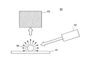
次に、本実施形態の特徴となる、異物検査装置8を用いてウエハ5上のインプリント領域に存在する異物を検出する異物検査工程を含むインプリント方法について説明する。図2は、異物検査装置を示す概略図である。異物検査装置60は、ウエハ61のショットに向けて光を照射する照明系62と、ショットからの散乱光を受光する検出系63とを備える。ここで、照明系62が光を照射し、ショットに異物が存在しない場合には、ショットに入射する入射光は、ウエハ61の表面上で正反射するので、検出系63は、反射光を受光しない。これに対して、図2に示すように、ショットに異物64が存在する場合には、入射光が異物64にて散乱するため、正反射角度以外でも光を反射する。したがって、検出系63は、この散乱光を受光することで異物64を検出する。なお、複数のショットにおける画像又は信号を比較することで、異物検査装置がこの相違点から異物の存在を判断してもよい。本実施形態のインプリント装置1では、異物検査装置8は、押印工程と塗布工程との間でウエハステージ6の移動と連動させて、好適には1ショットずつ異物検査を実施する。これにより、モールドとウエハ61上の樹脂と押し付ける押印工程の前にウエハ61の表面全面にて行う場合に比べて検査時間を短くできる。また、異物検査工程と押印工程との間の時間を短くできるため、新たに異物が付着する可能性が低くなる。
Next, an imprint method including a foreign matter inspection process for detecting foreign matter existing in an imprint area on the
図3は、本実施形態のインプリント工程の流れを示すフローチャートである。また、図4は、図3に示すインプリント工程の各工程に対応したインプリント装置1の各構成要素の動きを示す概略図である。ここで、制御装置9は、前のショット(第1ショット)に対する第1インプリント工程(ステップS100)が終了したウエハ5上の次のショット(第2ショット15)にて第2インプリント工程を実行する。この場合、まず、制御装置9は、第2ショット15に対して樹脂を塗布するために、図4(a)に示すように、第1塗布装置7aの塗布位置に第2ショット15が位置するように、X方向+側から−側へウエハステージ6を駆動する(ステップS101)。このとき、第2ショット15は、図4(b)に示すように、モールド3と第1塗布装置7aとの間に位置する第1異物検査装置8aの検査位置を通過する。そこで、制御装置9は、第1異物検査装置8aに対して第2ショット15の表面上の異物検査を実施させる(異物検査工程:ステップS102)。ここで、制御装置9は、第1異物検査装置8aによる検査結果に基づいて、第2ショット15の表面上に異物があるかどうかを判定する(ステップS103)。ステップS103にて、制御装置9は、異物が存在しないと判断した場合(No)、図4(c)に示すようにそのままウエハステージ6の駆動を続け、第1塗布装置7aの塗布位置に第2ショット15を位置させて樹脂を塗布させる(塗布工程:ステップS104)。次に、制御装置9は、モールド3の押印位置に第2ショット15が位置するように、X方向−側から+側へウエハステージ6を駆動する(ステップS105)。そして、制御装置9は、第2ショット15に対して押印工程を実行し、樹脂を硬化させた後、離型工程を実行し(ステップS106)、第2インプリント工程を終了する(ステップS107)。
FIG. 3 is a flowchart showing the flow of the imprint process of this embodiment. FIG. 4 is a schematic diagram showing the movement of each component of the
一方、ステップS103にて、制御装置9は、第2ショット15の表面上に異物が存在すると判断した場合(Yes)、通常の塗布及び押印工程を回避する回避工程に移行する(ステップS108)。この回避工程では、例えば、制御装置9は、第2ショット15に対して塗布及び押印工程を行わず、第2インプリント工程を終了する。これにより、ウエハ5の表面上に異物が存在したままの押印動作を回避することができるので、モールド3に形成された凹凸パターンの破壊を抑止することができる。
On the other hand, if the
なお、ステップS108における回避工程では、上記の他、例えば、制御装置9は、第2ショット15に対して塗布工程のみを実行する方法もある。即ち、半導体デバイスの製造工程に含まれるエッチング工程等の後工程を考慮すると、異物が存在する第2ショット15のみにインプリント工程を実施しない場合、正常にインプリント工程を実施した他のショットの構造との差異が発生する。そこで、この回避工程において、制御装置9は、第2ショット15の一面に樹脂を塗布させる塗布工程のみを実行することで、この差異を減らすことができる。その他、この回避工程において、例えば、制御装置9は、後の全てのインプリント工程を停止するという方法もある。この場合、一旦全てのインプリント工程を停止することで、異物が付着した原因等を特定し、その原因を取り除くことで、新たにインプリント工程を実施することができる。
In addition, in the avoidance process in step S108, in addition to the above, for example, there is a method in which the
この図3及び4に示すインプリント工程を、本実施形態のインプリント装置1は、複数のショットに対して順次、第1塗布装置7a及び第1異物検査装置8aと、これらに対向する第2塗布装置7b及び第2異物検査装置8bとで交互に実施する。即ち、例えば、上記第2ショット15に対する第2インプリント工程では、ステップS105における押印工程への移行の際、ウエハステージ6は、X方向−側から+側へ移動する。したがって、次の第3ショット(不図示)にインプリント工程を実施する際には、制御装置9は、そのままウエハステージ6をX方向−側から+側へ移動させて、第2塗布装置7b及び第2異物検査装置8bを利用して、第3インプリント工程を実行する。これにより、インプリント装置1は、複数のショットに対する個々のインプリント工程をウエハステージ6の移動方向に合わせて平行に実施するので、生産性を低下させることがない。
3 and 4, the
以上のように、本実施形態のインプリント装置1によれば、生産性を低下させることなく、インプリント領域に存在する異物を効率良く検出することができる。
As described above, according to the
(第2実施形態)
次に、本発明の第2実施形態に係るインプリント装置について説明する。図5は、本実施形態のインプリント装置20の構成を示す概略図である。なお、図5において、図1のインプリント装置1と同一構成のものには同一の符号を付し、説明を省略する。このインプリント装置20の特徴は、塗布装置7と異物検査装置8とを、第1実施形態では、モールド保持装置4から順に、異物検査装置8、塗布装置7と配置するのに対して、これとは逆に、塗布装置21を挟んで異物検査装置22を配置する点にある。
(Second Embodiment)
Next, an imprint apparatus according to the second embodiment of the present invention will be described. FIG. 5 is a schematic diagram illustrating a configuration of the
図6は、本実施形態のインプリント工程の流れを示すフローチャートである。また、図7は、図6に示すインプリント工程の各工程に対応したインプリント装置20の各構成要素の動きを示す概略図である。この場合も、制御装置9は、前のショット(第1ショット)に対する第1インプリント工程(ステップS200)が終了したウエハ5上の次のショット(第2ショット25)にて第2インプリント工程を実行する。まず、制御装置9は、第2ショット25に対して樹脂を塗布するために、図7(a)に示すように、第1塗布装置21aの塗布位置に向けて、X方向+側から−側へウエハステージ6を駆動する(ステップS201)。ここで、制御装置9は、図7(b)に示すように、第2ショット25が第1塗布装置21aの塗布位置に位置しても、そのままウエハステージ6を移動させる。そして、制御装置9は、第2ショット25を、その先に配置された第1異物検査装置22aの検査位置を通過させて、第1異物検査装置22aに対して第2ショット25の表面上の第1回目の異物検査を実施させる(第1異物検査工程:ステップS202)。ここで、制御装置9は、第1異物検査装置22aによる第1回目の検査結果に基づいて、第2ショット25の表面上に異物があるかどうかを判定する(ステップS203)。このステップS203にて、制御装置9は、異物が存在しないと判断した場合(No)、図7(c)に示すように、これまでの移動方向とは反対にX方向−側から+側へウエハステージ6を駆動する。そして、制御装置9は、第2ショット25を、その先に配置された第1異物検査装置22aの検査位置を通過させて、第1異物検査装置22aに対して第2ショット25の表面上の第2回目の異物検査を実施させる(第2異物検査工程:ステップS204)。ここで、制御装置9は、第1異物検査装置22aによる第2回目の検査結果に基づいて、第2ショット25の表面上に異物があるかどうかを判定する(ステップS205)。ステップS205にて、制御装置9は、異物が存在しないと判断した場合(No)、図7(d)に示すようにそのままウエハステージ6の駆動を続け、第1塗布装置21aの塗布位置に第2ショット25を位置させて樹脂を塗布する(塗布工程:ステップS206)。次に、制御装置9は、モールド3の押印位置に第2ショット25が位置するように、そのままウエハステージ6を駆動する(ステップS207)。そして、制御装置9は、第2ショット25に対して押印工程を実行し、樹脂を硬化させた後、離型工程を実行し(ステップS208)、第2インプリント工程を終了する(ステップS209)。
FIG. 6 is a flowchart showing the flow of the imprint process of this embodiment. FIG. 7 is a schematic diagram showing the movement of each component of the
一方、ステップS203、及び205のいずれかにおいて、制御装置9は、第2ショット25の表面上に異物が存在すると判断した場合(Yes)、通常の塗布及び押印工程を回避する回避工程に移行する(ステップS210)。この回避工程の内容は、第1実施形態におけるステップS108における回避工程と同様である。また、この図6及び7に示すインプリント工程を、複数のショットに対して順次、各塗布装置21及び各異物検査装置22にて交互に実施することも、第1実施形態と同様である。
On the other hand, in any of steps S203 and 205, when the
このように、本実施形態のインプリント装置20によれば、第1実施形態と同様の効果を奏すると共に、異物検査装置22は、1つのインプリント工程において、同じショットに対して2回異物検査を実施するので、異物検査の精度を向上させることができる。
As described above, according to the
なお、本実施形態では、異物検査装置22による2回の異物検査は、ウエハステージ6の加減速中での計測となるため、その検査結果に考慮を要する。即ち、異物検査装置22が同じ粒径の異物を同じ時間で計測したと仮定すると、ウエハステージ6の移動速度が速い場合は、散乱光の受光量が少なく、一方、移動速度が遅い場合は、受光量が多くなる。したがって、制御装置9は、異物の有無の判定には、ウエハステージ6の移動速度に応じた補正値を加味し出力する。但し、本実施形態における異物検査装置22の設置位置は、ウエハステージ6の折り返し移動地点にあり、これにより、ウエハステージ6の移動速度が一旦低下するので、異物検査を精度良く行うには有利である。
In this embodiment, since the two foreign substance inspections by the foreign substance inspection apparatus 22 are measurements during acceleration / deceleration of the wafer stage 6, the inspection result needs to be considered. That is, assuming that the foreign matter inspection apparatus 22 measures foreign matter having the same particle diameter in the same time, when the moving speed of the wafer stage 6 is fast, the amount of scattered light received is small, whereas when the moving speed is slow, The amount of light received increases. Therefore, the
(第3実施形態)
次に、本発明の第3実施形態に係るインプリント装置について説明する。本実施形態のインプリント装置では、上記実施形態に示す異物検査装置8(22)が、ウエハステージ6の移動方向に合わせて、この移動方向と平行に移動可能である点にある。近年、更に生産性を向上させるために、ウエハステージ6の移動速度は、高速化が進んでいる。したがって、異物検査装置8を固定したままでは、その検出位置を通過するウエハ5の移動速度が速すぎて、異物を検出不能、又は検出精度が劣化する場合も考えられる。そこで、本実施形態では、ウエハステージ6の移動に対して異物検査装置8を同期させ、それぞれ同じタイミングで異なる速度で平行に移動させることで相対速度を低下させる。これにより、異物検査装置8による異物検査の精度を向上させることができる。
(Third embodiment)
Next, an imprint apparatus according to a third embodiment of the present invention will be described. In the imprint apparatus according to the present embodiment, the foreign matter inspection apparatus 8 (22) shown in the above embodiment can move in parallel with the movement direction of the wafer stage 6 in accordance with the movement direction of the wafer stage 6. In recent years, in order to further improve productivity, the moving speed of the wafer stage 6 has been increased. Therefore, if the foreign substance inspection apparatus 8 is fixed, the movement speed of the
(第4実施形態)
次に、本発明の第4実施形態に係るインプリント装置について説明する。図8は、本実施形態のインプリント装置による各ショットへの樹脂の塗布状況を示す概略図である。図8において、ウエハ5の各ショットに付した英字は、後述の図9に示す各ショットに対応する。また、各ショットの表面上において、記載がないものは「未処理ショット」、黒丸が記載されたものは「樹脂塗布済みショット」、及び、黒三角が記載されたものは「インプリント工程済みショット」をそれぞれ示す。なお、図8に示すインプリント装置の構成は、説明のために、上記第2実施形態のインプリント装置20と同一構成とするが、例えば、第1実施形態のインプリント装置1と同一構成でもよい。また、図9は、ウエハ5上のショットのレイアウトを示す概略図である。本実施形態では、図9に示すように、ウエハ5のほぼ中心に位置するショットから、ウエハステージ6の移動方向に合わせて左右に領域を分割して考える。そして、左側の第1領域Lに配置される一列の複数のショットをウエハ5の外周部のものから順に、SA、SB、SCと設定し、一方、右側の第2領域Rに配置される同列の複数のショットをウエハ5の内周部のものから順に、SA´、SB´、SC´と設定する。その上で、本実施形態のインプリント装置の特徴は、あるショットに対する押印工程、硬化工程、または離型工程を含むインプリント工程を実施している間に、別のショットに対する異物検査工程を実施する点にある。
(Fourth embodiment)
Next, an imprint apparatus according to a fourth embodiment of the present invention will be described. FIG. 8 is a schematic diagram showing the state of resin application to each shot by the imprint apparatus of this embodiment. In FIG. 8, the alphabetic characters given to each shot of the
図10は、本実施形態のインプリント工程の流れを示すフローチャートである。まず、制御装置9は、予め樹脂が塗布されたショット(第1インプリント領域)SA´に対してインプリント工程を実行する(ステップS301A)。このとき、制御装置9は、図8(a)に示すように、ショットSA´へのインプリント工程と平行して、第1異物検査装置22aにより、ショットSAの表面上の異物検査を実行する(ステップS301B)。次に、制御装置9は、X方向−側から+側へウエハステージ6を駆動させ、第1塗布装置21aにて、異物検査が終了したショットSAに樹脂を塗布する(ステップS302B)。次に、制御装置9は、再度、X方向−側から+側へウエハステージ6を駆動させてショットSAを押印位置に合わせ、ショットSAに対するインプリント工程を実行する(ステップS303A)。このとき、制御装置9は、図8(b)に示すように、ショットSAへのインプリント工程と平行して、第2異物検査装置22bにより、ショットSB´の表面上の異物検査を実行する(ステップS303C)。次に、制御装置9は、X方向+側から−側へウエハステージ6を駆動させ、第2塗布装置21bにて、異物検査が終了したショットSB´に樹脂を塗布する(ステップS304C)。次に、制御装置9は、再度、X方向+側から−側へウエハステージ6を駆動させてショットSB´を押印位置に合わせ、ショットSB´に対するインプリント工程を実行する(ステップS305A)。以降、制御装置9は、ステップS305B、ステップS306Bと、上記のインプリント工程を所望のショット数に合わせて繰り返す。なお、本実施形態では、各異物検査装置22a、22bは、第3実施形態と同様に、ウエハステージ6の移動に対して同期して平行移動しつつ、異物検査を実施することが望ましい。また、例えば、モールド保持装置4(モールドベース11)の大きさや、モールド3と塗布装置21、及び異物検査装置22の各相対位置に起因して、上記インプリント工程において異物検査ができないショットが存在する場合もある。しかしながら、このようなショットの数は、全ショット数よりも十分に少ないので、予めこのインプリント工程とは別に異物検査を実施することで対応可能である。
FIG. 10 is a flowchart showing the flow of the imprint process of this embodiment. First, the
このように、本実施形態のインプリント装置によれば、あるショットに対するインプリント工程を実施している間に、別の未処理ショットに対する異物検査工程を実施する。この場合のインプリント工程、すなわちモールド3のパターン面と樹脂とが接触した状態を含む工程では、ウエハステージ6は、停止している。しかしながら、このインプリント工程を繰り返す複数のショットに対する一連の動作で見れば、本実施形態の異物検査工程もウエハステージ6の移動と連動した流れで実施されることになる。したがって、上記実施形態の効果において、更に生産性の向上に有利となる。
Thus, according to the imprint apparatus of the present embodiment, the foreign matter inspection process for another unprocessed shot is performed while the imprint process for a certain shot is being performed. In the imprint process in this case, that is, the process including the state where the pattern surface of the
(第5実施形態)
次に、本発明の第5実施形態に係るインプリント装置について説明する。図11は、本実施形態のインプリント装置30の構成を示す概略図である。特に、図11(a)及び11(b)は、Z方向上面から見た平面図である。上記実施形態では、塗布装置と異物検査装置とのそれぞれを、モールド保持装置4を基準としてウエハステージ6の移動方向の同軸上に設置する。これに対して、本実施形態のインプリント装置30の特徴は、モールド保持装置4を基準として、塗布装置31をウエハステージ6の移動方向と同軸のX軸上に設置し、一方、異物検査装置32をウエハステージ6の移動方向と直交するY軸上に設置する。なお、インプリント装置30のその他の構成は、第1実施形態と同一であるので、同一の符号を付し、説明を省略する。
(Fifth embodiment)
Next, an imprint apparatus according to a fifth embodiment of the present invention will be described. FIG. 11 is a schematic diagram illustrating a configuration of the
ここで、2箇所に設置された異物検査装置32a、32bは、通常、モールド保持装置4と一体で(同期して)移動するが、この同期移動とは別に、移動方向(X方向)と、直交する方向(Y方向)とにも単体で移動可能とする。この異物検査装置32は、図11に示すように、計測範囲(計測長さ)を適宜変更することも可能である。即ち、例えば、図11(a)に示すように、異物検査装置32の計測範囲をY方向に沿って長くなるように設定すると、X方向に対してスキャン計測するのに効率的である。また、この場合、異物検査装置32をY方向に適宜移動させることで、検査対象となるショットの列を変更し、ショットのレイアウトに合わせた検査列の最適化が可能となる。一方、図11(b)に示すように、異物検査装置32の計測範囲をX方向に沿って長くなるように設定すると、Y方向に対してスキャン計測するのに効率的である。この場合も、図11(a)の説明とは逆に、異物検査装置32をX方向に適宜移動させることで、ショットのレイアウトに合わせた検査列の最適化が可能となる。
Here, the foreign
次に、異物検査時のウエハ5に対するモールド保持装置4と異物検査装置32との動きについて詳説する。図11(c)は、モールド保持装置4と異物検査装置32との動きを示す平面図である。なお、インプリント装置30の構成としては、図11(a)を採用するものとする。ここで、インプリント装置30は、黒く塗りつぶしたショット33に対して押印工程を実施していると仮定する。このとき、モールド3の凹凸パターンに樹脂が充填されるのには、比較的長い時間を要する。そこで、2つの異物検査装置32a、32bは、この間にそれぞれX方向にスキャン計測し、各検査列のショット上に異物がないかどうかを検査する。そして、インプリント装置30は、ショット33の列に対してインプリント工程を完了させると、既に異物検査が終了した別の検査列に対してインプリント工程を実施する。なお、例えば、異物検査装置32の計測範囲が、複数の列に掛かるほど広ければ、異物検査装置32は、同時に複数の列を検査してもよい。また、樹脂の充填時間に更に余裕があれば、異物検査装置32は、Y方向に移動し、検査列を自ら変更して異物検査を継続してもよい。このように、本実施形態のインプリント装置30によれば、複数のショット列に対してインプリント工程と、異物検査工程とを平行して実施するので、上記実施形態の効果において、更に生産性の向上に有利となる。
Next, the movement of the
(物品の製造方法)
物品としてのデバイス(半導体集積回路素子、液晶表示素子等)の製造方法は、上述したインプリント装置を用いて基板(ウエハ、ガラスプレート、フィルム状基板)にパターンを形成する工程を含む。更に、該製造方法は、パターンが形成された基板をエッチングする工程を含みうる。なお、パターンドメディア(記録媒体)や光学素子等の他の物品を製造する場合には、該製造方法は、エッチングの代わりに、パターンが形成された基板を加工する他の処理を含みうる。本実施形態の物品の製造方法は、従来の方法に比べて、物品の性能・品質・生産性・生産コストの少なくとも1つにおいて有利である。
(Product manufacturing method)
A method for manufacturing a device (semiconductor integrated circuit element, liquid crystal display element, etc.) as an article includes a step of forming a pattern on a substrate (wafer, glass plate, film-like substrate) using the above-described imprint apparatus. Furthermore, the manufacturing method may include a step of etching the substrate on which the pattern is formed. In the case of manufacturing other articles such as patterned media (recording media) and optical elements, the manufacturing method may include other processes for processing a substrate on which a pattern is formed instead of etching. The method for manufacturing an article according to this embodiment is advantageous in at least one of the performance, quality, productivity, and production cost of the article as compared with the conventional method.
以上、本発明の好ましい実施形態について説明したが、本発明は、これらの実施形態に限定されず、その要旨の範囲内で種々の変形及び変更が可能である。 As mentioned above, although preferable embodiment of this invention was described, this invention is not limited to these embodiment, A various deformation | transformation and change are possible within the range of the summary.
1 インプリント装置
3 モールド
4 モールド保持装置
5 ウエハ
6 ウエハステージ
7a 第1塗布装置
7b 第2塗布装置
8a 第1異物検査装置
8b 第2異物検査装置
9 制御手段
DESCRIPTION OF
Claims (12)
前記モールドを保持する保持手段と、
前記基板における前記樹脂のパターンを形成するインプリント領域に異物が存在するかどうかを検査する異物検査手段と、
前記インプリント領域に前記未硬化樹脂を塗布する塗布手段と、
前記保持手段に対して前記インプリント領域を相対的に移動させる移動手段と、
前記保持手段、前記異物検査手段、前記塗布手段、及び前記移動手段の動作を制御する制御手段と、
を備え、
前記移動手段は、前記異物検査手段による検査位置、前記塗布手段による塗布位置、及び前記保持手段による押印位置のそれぞれに前記インプリント領域を移動可能であり、
前記制御手段は、前記移動手段により前記インプリント領域を前記塗布位置に移動させた後に当該移動方向とは反対の方向に移動させて前記インプリント領域を前記押印位置に位置させ、さらに、前記移動方向の切り替えにおける加速中または減速中に前記異物検査手段に対して前記インプリント領域の検査を実施させることを特徴とするインプリント装置。 An imprint apparatus for forming a pattern by bringing an uncured resin applied to a substrate into contact with a pattern surface of a mold,
Holding means for holding the mold;
Foreign matter inspection means for inspecting whether foreign matter is present in the imprint region for forming the resin pattern on the substrate;
Application means for applying the uncured resin to the imprint region;
Moving means for moving the imprint area relative to the holding means;
Control means for controlling operations of the holding means, the foreign matter inspection means, the application means, and the moving means;
With
The moving means can move the imprint region to each of an inspection position by the foreign substance inspection means, an application position by the application means, and a stamp position by the holding means,
The control means moves the imprint area to the application position by the moving means and then moves the imprint area in the direction opposite to the movement direction to position the imprint area at the stamping position. An imprint apparatus that causes the foreign matter inspection means to inspect the imprint area during acceleration or deceleration during direction switching .
前記制御手段は、前記塗布手段による前記未硬化樹脂の塗布の前に、前記検査を実施させることを特徴とする請求項1に記載のインプリント装置。 The foreign substance inspection means, said holding means, and said coating means is Installation on the same axis,
The imprint apparatus according to claim 1, wherein the control unit causes the inspection to be performed before the application of the uncured resin by the application unit.
前記制御手段は、前記減速時における検査が終了した後、前記インプリント領域を前記移動方向とは反対の方向へ移動させて、加速時に、再度、前記インプリント領域の検査を実施させることを特徴とする請求項4に記載のインプリント装置。 It said application means is Installation between the holding means and the foreign substance inspection means,
The control means moves the imprint area in a direction opposite to the moving direction after the inspection at the time of deceleration is completed, and causes the imprint area to be inspected again at the time of acceleration. The imprint apparatus according to claim 4.
前記基板上に前記インプリント領域が複数ある場合には、
前記制御手段は、前記+側に配置される第1異物検査手段、及び第2塗布手段と、前記−側に配置される第2異物検査手段、及び第2塗布手段とにより、前記複数のインプリント領域に対して交互に前記検査、及び前記樹脂の塗布を実施させることを特徴とする請求項3又は4に記載のインプリント装置。 The foreign matter inspection means and the application means are installed one by one on the + side and the − side on the same axis as the moving direction of the imprint region with respect to the installation position of the holding means,
When there are a plurality of the imprint areas on the substrate,
The control means includes the first foreign matter inspection means and the second application means arranged on the + side, and the second foreign matter inspection means and the second application means arranged on the − side. The imprint apparatus according to claim 3, wherein the inspection and the application of the resin are alternately performed on a print region.
前記モールドを保持する保持手段と、
前記基板における前記樹脂のパターンを形成するインプリント領域に異物が存在するかどうかを検査する異物検査手段と、
前記インプリント領域に前記未硬化樹脂を塗布する塗布手段と、
前記保持手段に対して前記インプリント領域を相対的に移動させる移動手段と、
前記保持手段、前記異物検査手段、前記塗布手段、及び前記移動手段の動作を制御する制御手段と、
を備え、
前記移動手段は、前記異物検査手段による検査位置、前記塗布手段による塗布位置、及び前記保持手段による押印位置のそれぞれに前記インプリント領域を移動可能であり、
前記異物検査手段は、前記移動手段の移動と同期し、前記移動手段と同じタイミング、かつ、前記移動手段と異なる速度で平行に移動可能であり、
前記制御手段は、前記移動手段による前記インプリント領域の動きと連動させて、前記異物検査手段に対して前記インプリント領域の検査を実施させることを特徴とするインプリント装置。 An imprint apparatus for forming a pattern by bringing an uncured resin applied to a substrate into contact with a pattern surface of a mold,
Holding means for holding the mold;
Foreign matter inspection means for inspecting whether foreign matter is present in the imprint region for forming the resin pattern on the substrate;
Application means for applying the uncured resin to the imprint region;
Moving means for moving the imprint area relative to the holding means;
Control means for controlling operations of the holding means, the foreign matter inspection means, the application means, and the moving means;
With
The moving means can move the imprint region to each of an inspection position by the foreign substance inspection means, an application position by the application means, and a stamp position by the holding means,
The foreign substance inspection means is synchronized movement of the same in the moving unit, the same timing as the moving means, and Ri movable parallel to Der at different speeds and the moving means,
Said control means, said moving said in conjunction with the movement of the imprint area by means, the imprint region feature and be Louis down printing apparatus that is an inspection with respect to the foreign substance inspection means.
前記モールドを保持する保持手段と、
前記基板における前記樹脂のパターンを形成するインプリント領域に異物が存在するかどうかを検査する異物検査手段と、
前記インプリント領域に前記未硬化樹脂を塗布する塗布手段と、
前記保持手段に対して前記インプリント領域を相対的に移動させる移動手段と、
前記保持手段、前記異物検査手段、前記塗布手段、及び前記移動手段の動作を制御する制御手段と、
を備え、
前記移動手段は、前記異物検査手段による検査位置、前記塗布手段による塗布位置、及び前記保持手段による押印位置のそれぞれに前記インプリント領域を移動可能であり、
前記塗布手段は、前記保持手段の設置位置を基準として、前記インプリント領域の移動方向と同軸上に少なくとも1つ設置され、かつ、
前記異物検査手段、前記保持手段の設置位置を基準として、前記インプリント領域の移動方向とは直交する軸上に少なくとも1つ設置され、
前記基板上に前記インプリント領域が複数ある場合には、
前記制御手段は、前記複数のインプリント領域のうち、前記検査、及び前記樹脂の塗布が完了したインプリント領域に対して、前記保持手段により前記未硬化樹脂と前記モールドとを押し付けている間に、前記異物検査手段により、前記塗布手段による前記未硬化樹脂の塗布の前のインプリント領域に対して検査を実施させることを特徴とするインプリント装置。 An imprint apparatus for forming a pattern by bringing an uncured resin applied to a substrate into contact with a pattern surface of a mold,
Holding means for holding the mold;
Foreign matter inspection means for inspecting whether foreign matter is present in the imprint region for forming the resin pattern on the substrate;
Application means for applying the uncured resin to the imprint region;
Moving means for moving the imprint area relative to the holding means;
Control means for controlling operations of the holding means, the foreign matter inspection means, the application means, and the moving means;
With
The moving means can move the imprint region to each of an inspection position by the foreign substance inspection means, an application position by the application means, and a stamp position by the holding means,
The application means is installed at least one on the same axis as the moving direction of the imprint area with reference to the installation position of the holding means, and
With reference to the installation position of the foreign substance inspection means and the holding means, at least one is installed on an axis orthogonal to the moving direction of the imprint area,
When there are a plurality of the imprint areas on the substrate,
The control unit is configured to press the uncured resin and the mold by the holding unit against the imprint region in which the inspection and the application of the resin are completed among the plurality of imprint regions. the by foreign substance inspection means, said application means according to the characteristics and to Louis down printing device that for the previous imprinting area to an inspection of the uncured resin coating.
前記異物が存在する前記インプリント領域にて、前記樹脂の塗布、及び前記未硬化樹脂と前記モールドとを押し付けを回避する、
前記異物が存在する前記インプリント領域にて、前記樹脂の塗布を実施し、前記押し付けを回避する、又は、
前記基板上の全てのインプリント領域にて、前記樹脂の塗布、及び前記押し付けを停止する、
のいずれか1つを実行することを特徴とする請求項1〜9のいずれか1項に記載のインプリント装置。 The control means, when the foreign matter inspection means detects the foreign matter,
In the imprint region where the foreign matter is present, avoid application of the resin and pressing the uncured resin and the mold.
In the imprint area where the foreign matter is present, apply the resin and avoid the pressing, or
In all imprint areas on the substrate, the application of the resin and the pressing are stopped.
The imprint apparatus according to claim 1, wherein any one of the following is executed.
前記基板を搭載して移動する移動手段と、
前記基板に前記未硬化樹脂を塗布する塗布手段と、
前記基板の複数のインプリント領域のうちの第1インプリント領域に前記パターン面を接触させている間、または、前記第1インプリント領域に前記パターンを形成した後に、前記第1インプリント領域とは異なるインプリント領域に前記未硬化樹脂を塗布するために前記基板を移動している間に、前記第1インプリント領域とは異なるインプリント領域に異物が存在するかどうかを検査する異物検査手段と、を備え、
前記移動手段は、前記インプリント領域を塗布がなされる位置に移動させた後に当該移動方向とは反対の方向に移動させて前記インプリント領域を前記パターンの形成がなされる位置に位置させ、
前記異物検査手段は、前記移動方向の切り替えにおける加速中または減速中に検査をすることを特徴とするインプリント装置。 An imprint apparatus for forming a pattern by bringing an uncured resin applied to a substrate into contact with a pattern surface of a mold,
A moving means for mounting and moving the substrate;
Application means for applying the uncured resin to the substrate;
The first imprint area and the first imprint area while the pattern surface is in contact with the first imprint area of the plurality of imprint areas of the substrate, or after the pattern is formed in the first imprint area Foreign matter inspection means for inspecting whether foreign matter exists in an imprint area different from the first imprint area while moving the substrate to apply the uncured resin to a different imprint area and, with a,
The moving means moves the imprint area to a position where application is performed and then moves the imprint area in a direction opposite to the movement direction to position the imprint area at a position where the pattern is formed,
The imprint apparatus according to claim 1, wherein the foreign matter inspection means inspects during acceleration or deceleration in switching of the moving direction .
前記工程で前記パターンを形成された基板を加工する工程と、
を有することを特徴とする物品の製造方法。
Forming a resin pattern on a substrate using the imprint apparatus according to claim 1;
Processing the substrate on which the pattern is formed in the step;
A method for producing an article comprising:
Priority Applications (4)
| Application Number | Priority Date | Filing Date | Title |
|---|---|---|---|
| JP2011255292A JP5850717B2 (en) | 2010-12-02 | 2011-11-22 | Imprint apparatus and article manufacturing method using the same |
| US13/305,990 US8893649B2 (en) | 2010-12-02 | 2011-11-29 | Imprint apparatus and article manufacturing method |
| US14/272,782 US9575407B2 (en) | 2010-12-02 | 2014-05-08 | Imprint apparatus and article manufacturing method |
| US15/400,081 US9778565B2 (en) | 2010-12-02 | 2017-01-06 | Imprint apparatus and article manufacturing method |
Applications Claiming Priority (3)
| Application Number | Priority Date | Filing Date | Title |
|---|---|---|---|
| JP2010269468 | 2010-12-02 | ||
| JP2010269468 | 2010-12-02 | ||
| JP2011255292A JP5850717B2 (en) | 2010-12-02 | 2011-11-22 | Imprint apparatus and article manufacturing method using the same |
Publications (3)
| Publication Number | Publication Date |
|---|---|
| JP2012134466A JP2012134466A (en) | 2012-07-12 |
| JP2012134466A5 JP2012134466A5 (en) | 2015-01-15 |
| JP5850717B2 true JP5850717B2 (en) | 2016-02-03 |
Family
ID=46162494
Family Applications (1)
| Application Number | Title | Priority Date | Filing Date |
|---|---|---|---|
| JP2011255292A Active JP5850717B2 (en) | 2010-12-02 | 2011-11-22 | Imprint apparatus and article manufacturing method using the same |
Country Status (2)
| Country | Link |
|---|---|
| US (3) | US8893649B2 (en) |
| JP (1) | JP5850717B2 (en) |
Families Citing this family (11)
| Publication number | Priority date | Publication date | Assignee | Title |
|---|---|---|---|---|
| JP5863286B2 (en) * | 2011-06-16 | 2016-02-16 | キヤノン株式会社 | Imprint method, imprint apparatus, and article manufacturing method |
| JP6525628B2 (en) * | 2015-02-13 | 2019-06-05 | キヤノン株式会社 | Imprint apparatus and method of manufacturing article |
| JP6438332B2 (en) * | 2015-03-18 | 2018-12-12 | キヤノン株式会社 | Imprint system and article manufacturing method |
| JP6821414B2 (en) * | 2016-12-13 | 2021-01-27 | キヤノン株式会社 | Imprinting equipment and manufacturing method of articles |
| JP6942487B2 (en) * | 2017-03-03 | 2021-09-29 | キヤノン株式会社 | Imprinting equipment, imprinting method, and article manufacturing method |
| JP6299910B2 (en) * | 2017-03-28 | 2018-03-28 | 大日本印刷株式会社 | Foreign matter inspection method, imprint method, and foreign matter inspection device |
| JP7138417B2 (en) * | 2017-08-03 | 2022-09-16 | キヤノン株式会社 | Foreign Matter Inspection Apparatus, Foreign Matter Inspection Method, Imprint Apparatus, and Article Manufacturing Method |
| WO2019151975A1 (en) * | 2018-01-30 | 2019-08-08 | Hewlett-Packard Development Company, L.P. | Alignment devices |
| CN108480139B (en) * | 2018-05-29 | 2024-04-05 | 天津爱码信自动化技术有限公司 | Intelligent coating and engraving machine |
| JP7278828B2 (en) * | 2019-03-26 | 2023-05-22 | キヤノン株式会社 | Molding method, molding apparatus, imprinting method, and article manufacturing method |
| US11908711B2 (en) * | 2020-09-30 | 2024-02-20 | Canon Kabushiki Kaisha | Planarization process, planarization system and method of manufacturing an article |
Family Cites Families (13)
| Publication number | Priority date | Publication date | Assignee | Title |
|---|---|---|---|---|
| JP3573587B2 (en) * | 1997-02-05 | 2004-10-06 | 株式会社ルネサステクノロジ | Micro-defect inspection method and apparatus, exposure method and semiconductor substrate manufacturing method |
| US6475410B1 (en) * | 1999-09-01 | 2002-11-05 | Tomey Corporation | Method and device for producing contact lens elements and injection mold used therefor |
| JP2002057097A (en) * | 2000-05-31 | 2002-02-22 | Nikon Corp | Aligner, and microdevice and its manufacturing method |
| JP4325084B2 (en) * | 2000-06-19 | 2009-09-02 | 東レ株式会社 | Coating method and color filter manufacturing method using the same |
| US6921615B2 (en) * | 2000-07-16 | 2005-07-26 | Board Of Regents, The University Of Texas System | High-resolution overlay alignment methods for imprint lithography |
| JP4393244B2 (en) * | 2004-03-29 | 2010-01-06 | キヤノン株式会社 | Imprint device |
| JP4533358B2 (en) * | 2005-10-18 | 2010-09-01 | キヤノン株式会社 | Imprint method, imprint apparatus and chip manufacturing method |
| JP4795300B2 (en) * | 2006-04-18 | 2011-10-19 | キヤノン株式会社 | Alignment method, imprint method, alignment apparatus, imprint apparatus, and position measurement method |
| WO2007124007A2 (en) * | 2006-04-21 | 2007-11-01 | Molecular Imprints, Inc. | Method for detecting a particle in a nanoimprint lithography system |
| JP5473266B2 (en) * | 2007-08-03 | 2014-04-16 | キヤノン株式会社 | Imprint method, substrate processing method, and semiconductor device manufacturing method by substrate processing method |
| JP2010027743A (en) * | 2008-07-16 | 2010-02-04 | Ebara Corp | Glass substrate for imprint, resist pattern forming method, and method and apparatus for inspecting glass substrate for imprint |
| JP4660581B2 (en) * | 2008-09-19 | 2011-03-30 | 株式会社東芝 | Pattern formation method |
| US8142704B2 (en) * | 2008-10-22 | 2012-03-27 | Molecular Imprints, Inc. | Imprint lithography system and method |
-
2011
- 2011-11-22 JP JP2011255292A patent/JP5850717B2/en active Active
- 2011-11-29 US US13/305,990 patent/US8893649B2/en active Active
-
2014
- 2014-05-08 US US14/272,782 patent/US9575407B2/en active Active
-
2017
- 2017-01-06 US US15/400,081 patent/US9778565B2/en active Active
Also Published As
| Publication number | Publication date |
|---|---|
| US20120141659A1 (en) | 2012-06-07 |
| US20170115559A1 (en) | 2017-04-27 |
| US9778565B2 (en) | 2017-10-03 |
| US20140246799A1 (en) | 2014-09-04 |
| US9575407B2 (en) | 2017-02-21 |
| US8893649B2 (en) | 2014-11-25 |
| JP2012134466A (en) | 2012-07-12 |
Similar Documents
| Publication | Publication Date | Title |
|---|---|---|
| JP5850717B2 (en) | Imprint apparatus and article manufacturing method using the same | |
| US10095117B2 (en) | Imprint apparatus | |
| JP5268524B2 (en) | Processing equipment | |
| US8678808B2 (en) | Imprint apparatus and article manufacturing method | |
| JP6021606B2 (en) | Imprint apparatus, article manufacturing method using the same, and imprint method | |
| JP6029268B2 (en) | Imprint apparatus and article manufacturing method using the same | |
| JP6300459B2 (en) | Imprint apparatus, imprint method, and article manufacturing method using the same | |
| JP4963718B2 (en) | Imprint method, imprint apparatus, and article manufacturing method using the same | |
| KR20190077295A (en) | Method of curing uncured material and method of manufacturing article | |
| US20130015599A1 (en) | Imprint apparatus, and method of manufacturing article | |
| JP2012124390A (en) | Imprint apparatus and method of manufacturing device | |
| JP2011171410A (en) | Imprint apparatus and article manufacturing method | |
| JP2012146699A (en) | Imprint device and manufacturing method of article using the same | |
| JP2012238674A (en) | Imprint apparatus and manufacturing method of goods | |
| JP6395352B2 (en) | Imprint apparatus, imprint method, and article manufacturing method using the same | |
| US20200307038A1 (en) | Molding method, molding apparatus, imprint method, method for manufacturing article, and article manufacturing system | |
| KR102059758B1 (en) | Imprint apparatus and article manufacturing method | |
| JP6450105B2 (en) | Imprint apparatus and article manufacturing method | |
| US20210132516A1 (en) | Imprint apparatus, imprint method, and article manufacturing method | |
| JP2019062164A (en) | Imprint device, imprint method, determination method of arrangement pattern of imprint material, and manufacturing method of article | |
| JP2015023151A (en) | Imprint device, imprint method, program, imprint system, and method of manufacturing article using them | |
| JP5611399B2 (en) | Processing equipment | |
| JP2013225616A (en) | Imprint method and method of manufacturing article using the same | |
| US20230112924A1 (en) | Substrate conveyance method, substrate conveyance apparatus, molding method, and article manufacturing method | |
| JP2016021442A (en) | Imprint device and method of manufacturing imprint device |
Legal Events
| Date | Code | Title | Description |
|---|---|---|---|
| A521 | Written amendment |
Free format text: JAPANESE INTERMEDIATE CODE: A523 Effective date: 20141121 |
|
| A621 | Written request for application examination |
Free format text: JAPANESE INTERMEDIATE CODE: A621 Effective date: 20141121 |
|
| A131 | Notification of reasons for refusal |
Free format text: JAPANESE INTERMEDIATE CODE: A131 Effective date: 20150728 |
|
| A521 | Written amendment |
Free format text: JAPANESE INTERMEDIATE CODE: A523 Effective date: 20150928 |
|
| TRDD | Decision of grant or rejection written | ||
| A01 | Written decision to grant a patent or to grant a registration (utility model) |
Free format text: JAPANESE INTERMEDIATE CODE: A01 Effective date: 20151102 |
|
| A61 | First payment of annual fees (during grant procedure) |
Free format text: JAPANESE INTERMEDIATE CODE: A61 Effective date: 20151201 |
|
| R151 | Written notification of patent or utility model registration |
Ref document number: 5850717 Country of ref document: JP Free format text: JAPANESE INTERMEDIATE CODE: R151 |