JP5473266B2 - Imprint method, substrate processing method, and semiconductor device manufacturing method by substrate processing method - Google Patents
Imprint method, substrate processing method, and semiconductor device manufacturing method by substrate processing method Download PDFInfo
- Publication number
- JP5473266B2 JP5473266B2 JP2008182297A JP2008182297A JP5473266B2 JP 5473266 B2 JP5473266 B2 JP 5473266B2 JP 2008182297 A JP2008182297 A JP 2008182297A JP 2008182297 A JP2008182297 A JP 2008182297A JP 5473266 B2 JP5473266 B2 JP 5473266B2
- Authority
- JP
- Japan
- Prior art keywords
- pattern
- processing
- region
- forming
- resin
- Prior art date
- Legal status (The legal status is an assumption and is not a legal conclusion. Google has not performed a legal analysis and makes no representation as to the accuracy of the status listed.)
- Expired - Fee Related
Links
Images


Classifications
-
- G—PHYSICS
- G03—PHOTOGRAPHY; CINEMATOGRAPHY; ANALOGOUS TECHNIQUES USING WAVES OTHER THAN OPTICAL WAVES; ELECTROGRAPHY; HOLOGRAPHY
- G03F—PHOTOMECHANICAL PRODUCTION OF TEXTURED OR PATTERNED SURFACES, e.g. FOR PRINTING, FOR PROCESSING OF SEMICONDUCTOR DEVICES; MATERIALS THEREFOR; ORIGINALS THEREFOR; APPARATUS SPECIALLY ADAPTED THEREFOR
- G03F7/00—Photomechanical, e.g. photolithographic, production of textured or patterned surfaces, e.g. printing surfaces; Materials therefor, e.g. comprising photoresists; Apparatus specially adapted therefor
- G03F7/0002—Lithographic processes using patterning methods other than those involving the exposure to radiation, e.g. by stamping
-
- B—PERFORMING OPERATIONS; TRANSPORTING
- B29—WORKING OF PLASTICS; WORKING OF SUBSTANCES IN A PLASTIC STATE IN GENERAL
- B29C—SHAPING OR JOINING OF PLASTICS; SHAPING OF MATERIAL IN A PLASTIC STATE, NOT OTHERWISE PROVIDED FOR; AFTER-TREATMENT OF THE SHAPED PRODUCTS, e.g. REPAIRING
- B29C33/00—Moulds or cores; Details thereof or accessories therefor
- B29C33/42—Moulds or cores; Details thereof or accessories therefor characterised by the shape of the moulding surface, e.g. ribs or grooves
- B29C33/424—Moulding surfaces provided with means for marking or patterning
-
- B—PERFORMING OPERATIONS; TRANSPORTING
- B82—NANOTECHNOLOGY
- B82Y—SPECIFIC USES OR APPLICATIONS OF NANOSTRUCTURES; MEASUREMENT OR ANALYSIS OF NANOSTRUCTURES; MANUFACTURE OR TREATMENT OF NANOSTRUCTURES
- B82Y10/00—Nanotechnology for information processing, storage or transmission, e.g. quantum computing or single electron logic
-
- B—PERFORMING OPERATIONS; TRANSPORTING
- B82—NANOTECHNOLOGY
- B82Y—SPECIFIC USES OR APPLICATIONS OF NANOSTRUCTURES; MEASUREMENT OR ANALYSIS OF NANOSTRUCTURES; MANUFACTURE OR TREATMENT OF NANOSTRUCTURES
- B82Y40/00—Manufacture or treatment of nanostructures
Description
本発明は、インプリント方法および基板の加工方法、基板の加工方法による半導体デバイスの製造方法に関する。
具体的には、基板上の樹脂に、モールドが有するパターンをインプリントするインプリント方法および基板の加工方法、基板の加工方法による半導体デバイスの製造方法に関するものである。
The present invention relates to an imprint method, a substrate processing method, and a semiconductor device manufacturing method using the substrate processing method.
Specifically, the present invention relates to an imprint method for imprinting a pattern of a mold onto a resin on a substrate, a substrate processing method, and a semiconductor device manufacturing method using the substrate processing method.
近年、モールド上の微細な構造を樹脂や金属等の被加工部材に転写する微細加工技術が開発され、注目を集めている。
この技術は、ナノインプリントあるいはナノエンボッシングなどと呼ばれ、数nmオーダーの分解能を持つため、ステッパ、スキャナ等の光露光機に代わる次世代の半導体製造技術としての期待が高まっている。
さらに、立体構造をウエハレベルで一括加工可能なため、フォトニッククリスタル等の光学素子、μ−TAS(Micro Total Analysis System)などのバイオチップの製造技術、等として幅広い分野への応用が期待されている。
In recent years, a fine processing technique for transferring a fine structure on a mold to a workpiece such as a resin or metal has been developed and attracts attention.
This technology is called nanoimprinting or nano-embossing, and has a resolution of the order of several nanometers. Therefore, there is an increasing expectation as a next-generation semiconductor manufacturing technology that can replace optical exposure machines such as steppers and scanners.
Furthermore, since the three-dimensional structure can be processed at the wafer level, it is expected to be applied to a wide range of fields such as optical elements such as photonic crystals and biochip manufacturing techniques such as μ-TAS (Micro Total Analysis System). Yes.
このような加工技術は、例えば半導体製造技術に適用する場合には、以下のように行われる。
基板(例えば半導体ウエハ)上に光硬化型の樹脂層を有するワークと、当該樹脂に所望の凹凸パターンが形成されたモールドを合わせて、両者の間に樹脂を充填させ、紫外光を照射することで樹脂を硬化させる。
これにより、樹脂層に上記パターンが転写されるので、この樹脂層をマスク層としてエッチング等を行い、基板へのパターン形成が行われる。
また、半導体のリソグラフィーにインプリントを用いる場合、製造するチップの大きさにあわせてモールドを作り、基板上への転写を繰り返し行うステップアンドリピート方式が適しているとされている。
その理由は、ウエハサイズの増加に伴う重ね合わせやモールドパターンそのものの積算誤差を減少して精度を向上させることができ、あるいはサイズの増加に伴うモールド作製のコストを削減することができるからである。
基板上に転写された樹脂層には、パターンの下地に一般に残膜と呼ばれる厚みが存在する。
これを除去することにより、基板の加工を行うためのマスク層が完成する。本明細書では、このマスク層をエッチングバリアと記すことにする。
Such a processing technique is performed as follows, for example, when applied to a semiconductor manufacturing technique.
A workpiece having a photo-curing resin layer on a substrate (for example, a semiconductor wafer) and a mold having a desired concavo-convex pattern formed on the resin, filled with the resin, and irradiated with ultraviolet light To cure the resin.
As a result, the pattern is transferred to the resin layer, and etching or the like is performed using the resin layer as a mask layer to form a pattern on the substrate.
In addition, when imprinting is used for semiconductor lithography, a step-and-repeat method in which a mold is made in accordance with the size of a chip to be manufactured and transfer onto a substrate is repeated is suitable.
The reason is that the accuracy can be improved by reducing the overlay error accompanying the increase in wafer size and the integration error of the mold pattern itself, or the cost of mold production accompanying the increase in size can be reduced. .
The resin layer transferred onto the substrate has a thickness generally called a remaining film on the base of the pattern.
By removing this, a mask layer for processing the substrate is completed. In this specification, this mask layer is referred to as an etching barrier.
従来例によるインプリント方法において、特許文献1では、上記したエッチングバリアを形成するに際し、UV硬化樹脂のみを単層で用い、全面をエッチングすることによりエッチングバリアを形成する方法が提案されている。
このようなプロセスを本明細書では単層プロセスと記すことにする。
また、全面をエッチングして均等に膜厚を減らす処理のことを、本明細書ではエッチバックと記すことにする。
In the imprint method according to the conventional example,
Such a process is referred to herein as a single layer process.
In addition, the process of etching the entire surface to uniformly reduce the film thickness is referred to as etch back in this specification.
また、特許文献2では、樹脂層とエッチング選択比の取れる材料を用いて反転パターンを形成する方法が提案されている。
この方法では、樹脂層の上に、樹脂層とエッチング選択比の取れる材料による反転層を塗布し、樹脂層の凸部が露出するまでエッチバックを行う。
最後に、樹脂層の凹部に埋め込まれた反転層をマスクに、樹脂層をエッチングする。
このようなプロセスを本明細書では反転プロセスと記すことにする。
この方法では、エッチングバリアはより垂直な加工形状となり、かつ寸法精度も高くなるとされている。
In this method, an inversion layer made of a material having an etching selectivity with respect to the resin layer is applied on the resin layer, and etching back is performed until the convex portions of the resin layer are exposed.
Finally, the resin layer is etched using the inversion layer embedded in the recess of the resin layer as a mask.
Such a process is referred to herein as an inversion process.
In this method, the etching barrier is assumed to have a more vertical processing shape and higher dimensional accuracy.
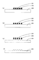
上記した従来例のインプリント方法によって、基板上にパターンを形成する場合、つぎのような問題が生じる場合がある。
すなわち、図8に示すように、1ショット分のインプリントを行った際、ショット外に樹脂が押し出され、モールド1251の縁に沿うように基板1253にはみ出し領域1254を形成してしまうことがある。
このはみ出し領域1254の樹脂層の膜厚は、ショット内の加工領域1255における樹脂層の膜厚よりも厚くなることが多い。
例えば、加工領域1255における樹脂層の膜厚や、パターンの凹凸が数十nm〜数百nm程度であるのに対し、はみ出し領域1254の樹脂層の厚さは数μm以上になることがある。
When a pattern is formed on a substrate by the above-described conventional imprint method, the following problem may occur.
That is, as shown in FIG. 8, when imprinting for one shot is performed, the resin is pushed out of the shot, and the
In many cases, the thickness of the resin layer in the
For example, the thickness of the resin layer in the
半導体リソグラフィーにインプリントを用いる場合、前述したようにステップアンドリピート方式が適しているとされているが、ステップアンドリピート方式により基板上への転写を繰り返し行った際には、はみ出し領域1254が各ショットに形成される。
このようなはみだし領域1254が形成されることにより、はみ出し領域の近傍と、はみ出し領域から離れたところでエッチングの特性が変化してしまうという問題が生じる場合がある。
例えば、凹凸パターンと比較してはるかに大きいオーダーの突起状の構造が近傍に存在する場合、エッチング中のプラズマの電界分布を乱したり、エッチングガスの流れを妨げてしまったりする場合がある。
また、エッチングは化学的な反応を含むことから、樹脂層の露出面積が非常に大きいはみ出し部分近傍では、はみ出し領域から離れたところと比べてエッチングガスの消費量が局所的に多く必要になってしまう場合がある。
このような現象により、はみ出し領域近傍と、はみ出し領域から離れたところでエッチングの特性が変化してしまうという問題が生じる場合がある。
When imprinting is used for semiconductor lithography, the step-and-repeat method is suitable as described above. However, when the transfer onto the substrate is repeatedly performed by the step-and-repeat method, the
The formation of such a
For example, in the case where a projecting structure having a much larger order than that of the concavo-convex pattern exists in the vicinity, the electric field distribution of plasma during etching may be disturbed or the flow of etching gas may be hindered.
Also, since etching involves a chemical reaction, the consumption of etching gas is required locally in the vicinity of the protruding portion where the exposed area of the resin layer is very large compared to the portion away from the protruding region. May end up.
Due to such a phenomenon, there may be a problem that the etching characteristics change near the protruding region and away from the protruding region.
本発明は、上記課題に鑑み、加工領域からはみ出した、はみ出し領域の樹脂層を容易に除去することが可能となるインプリント方法および基板の加工方法、基板の加工方法による半導体デバイスの製造方法を提供することを目的とするものである。 In view of the above problems, the present invention provides an imprint method, a substrate processing method, and a method for manufacturing a semiconductor device by a substrate processing method that can easily remove a resin layer in the protrusion region that protrudes from the processing region. It is intended to provide.
本発明は、つぎのように構成したインプリント方法および基板の加工方法、基板の加工方法による半導体デバイスの製造方法を提供するものである。
本発明のインプリント方法は、基板上の樹脂に、モールドのパターンをインプリントしてパターンを形成する工程を、複数回繰り返し行うインプリント方法であって、第1回目のパターンを形成する工程と、第2回目のパターンを形成する工程と、を有し、前記第1回目のパターンを形成する工程は、前記基板上に形成された樹脂に、前記モールドを接触させ、該モールドのパターンに対応する凹凸パターンを形成した第1の加工領域と、該第1の加工領域の周囲に前記樹脂によるはみ出し領域を形成する工程と、前記第1の加工領域の上に、該第1の加工領域を保護する第1の保護層を形成する工程と、前記第1の保護層によって、前記第1の加工領域の樹脂層に形成されたパターンが除去されないように保護しながら、前記はみ出し領域の樹脂層を除去する工程と、を有し、前記第2回目のパターンを形成する工程は、前記はみ出し領域を含む前記第1の加工領域と隣接する領域に形成された樹脂に前記モールドを接触させ、第2の加工領域を形成する工程と、前記第2の加工領域の樹脂層に、該第2の加工領域を保護する第2の保護層を形成する工程と、前記第1及び第2の保護層によって、前記第1及び第2の加工領域の樹脂層に形成されたパターンが除去されないように保護しながら、前記第2の加工領域の周囲にはみ出した樹脂を除去する工程と、
を有することを特徴とする。
また、本発明のインプリント方法は、前記第1回目のパターンを形成する工程において、第1方向または該第1方向と直交する第2方向の少なくともいずれかの方向に、前記第1の加工領域に複数の加工領域を形成するに際し、
前記複数の加工領域における各加工領域の間隔を、前記加工領域の幅の長さの整数倍とすることを特徴とする。
また、本発明のインプリント方法は、前記加工領域の幅の長さに、前記モールドの加工誤差および前記基板と前記モールドの位置合わせ誤差による調整量を加えた長さが含まれていることを特徴とする。
また、本発明のインプリント方法は、前記パターンを形成する工程を3回繰り返し行うインプリント方法であって、
前記第1の加工領域において前記第1方向に形成される各加工領域の間隔を、前記第1の加工領域の幅の長さの2倍とすると共に、前記第2方向における加工領域は互いに隣接しない間隔として、前記各加工領域を形成する工程と、
前記第2回目のパターンを形成する工程の後に、前記第2の加工領域と隣接する領域に第3の加工領域を形成する工程と、
を有することを特徴とする。
また、本発明のインプリント方法は、前記パターンを形成する工程を複数回繰り返し行うに際し、各パターンを形成する工程に異なるモールドを用いることを特徴とする。
また、本発明の基板の加工方法は、上記したいずれかに記載のインプリント方法により、基板上の樹脂にインプリントされたパターンをマスクとして前記基板を加工する工程を有することを特徴とする。
また、本発明の半導体デバイスの製造方法は、上記した基板の加工方法を用いて構造体を形成する工程を有することを特徴とする。
The present invention provides an imprint method, a substrate processing method, and a semiconductor device manufacturing method using the substrate processing method configured as follows.
Imprinting method of the present invention, the resin on the base plate, forming a pattern of the mold pattern by imprinting, a plurality of times repeated imprinting method, the step of forming the first round of pattern And a step of forming a second pattern, wherein the step of forming the first pattern comprises bringing the mold into contact with a resin formed on the substrate, and forming a pattern on the mold. A first processing region in which a corresponding concavo-convex pattern is formed; a step of forming a protruding region of the resin around the first processing region; and the first processing region on the first processing region Forming the first protective layer for protecting the protrusion, and the protruding region while protecting the pattern formed on the resin layer in the first processing region from being removed by the first protective layer. Includes a step of removing the resin layer, a step of forming the second round of pattern, is brought into contact with the mold resin formed in the adjacent region and the first processing region including the protruding region A step of forming a second processing region, a step of forming a second protective layer for protecting the second processing region on the resin layer of the second processing region, and the first and second steps Removing the resin protruding around the second processing region while protecting the pattern formed on the resin layer in the first and second processing regions from being removed by a protective layer;
It is characterized by having.
Further, in the imprint method of the present invention, in the step of forming the first pattern, the first processing region is arranged in at least one of a first direction or a second direction orthogonal to the first direction. When forming a plurality of processing areas in
The interval between the machining areas in the plurality of machining areas is an integral multiple of the width of the machining area.
Further, the imprint method of the present invention includes a length obtained by adding an adjustment amount due to a processing error of the mold and a positioning error of the substrate and the mold to the length of the width of the processing region. Features.
The imprint method of the present invention is an imprint method in which the step of forming the pattern is repeated three times,
In the first processing region, the interval between the processing regions formed in the first direction is twice the width of the first processing region, and the processing regions in the second direction are adjacent to each other. A step of forming each processing region as an interval not to be performed;
After the step of forming the second pattern, forming a third processing region in a region adjacent to the second processing region;
It is characterized by having.
The imprinting method of the present invention is characterized in that different molds are used for the steps of forming each pattern when the step of forming the pattern is repeated a plurality of times.
In addition, the substrate processing method of the present invention includes a step of processing the substrate by using the pattern imprinted on the resin on the substrate as a mask by any of the imprint methods described above.
The semiconductor device manufacturing method of the present invention includes a step of forming a structure using the above-described substrate processing method.
本発明によれば、加工領域からはみ出した、はみ出し領域の樹脂層を容易に除去することが可能となるインプリント方法および基板の加工方法、基板の加工方法による半導体デバイスの製造方法を実現することができる。 According to the present invention, it is possible to realize an imprint method, a substrate processing method, and a semiconductor device manufacturing method using a substrate processing method that can easily remove the resin layer protruding from the processing region. Can do.
本発明を実施するための最良の形態を、以下の実施例により説明する。 The best mode for carrying out the present invention will be described by the following examples.
以下に、本発明の実施例について、図を用いて説明する。
なお、以下の各図において、同一または対応する部分には同一の符号が付されている。
[実施例1]
実施例1では、図1と図2を用いて、本発明を適用したインプリント方法について説明する。
Embodiments of the present invention will be described below with reference to the drawings.
In the following drawings, the same or corresponding parts are denoted by the same reference numerals.
[Example 1]
In the first embodiment, an imprint method to which the present invention is applied will be described with reference to FIGS. 1 and 2.
まず、図1において、工程101では、基板上に形成した樹脂層にモールドのパターンを転写する。
具体的には、図2(a)に示すように、基板203上に樹脂層202を形成する。
その後、図2(b)のように、モールド201を樹脂層202に接触させてから、樹脂層202を硬化する。このとき、モールド201により加工領域205から押し出された樹脂層202がはみ出し領域204となって形成される。
そして、図2(c)のように、モールド201を樹脂層202から剥離し、モールド201上のパターンを樹脂層202上に転写する。
これにより、基板上の樹脂に、モールドが有するパターンに対応する凹凸パターンが形成された加工領域205と、該加工領域の全周に前記樹脂によるはみ出し領域204が形成された第1層が形成される。
モールド201は表面に所望の凹凸パターンを有し、材質には、例えばシリコン、石英、サファイア等が用いられる。
また、パターンのある表面は、一般的な離型処理として、フッ素系シランカップリング剤等を用いた離型処理を施す。なお、本明細書では、離型処理により形成される離型層を含めてモールドと称する。
樹脂層202に用いる材料は、アクリル系、あるいはエポキシ系の光硬化性樹脂、熱硬化性樹脂、熱可塑性樹脂等が、適用可能である。
First, in FIG. 1, in step 101, a mold pattern is transferred to a resin layer formed on a substrate.
Specifically, as illustrated in FIG. 2A, a
Thereafter, as shown in FIG. 2B, after the
Then, as shown in FIG. 2C, the
As a result, a processed
The
In addition, the surface having a pattern is subjected to a release treatment using a fluorine-based silane coupling agent or the like as a general release treatment. In this specification, a mold including a release layer formed by a release process is referred to as a mold.
As a material used for the
次に、図1に戻って、工程102では、工程101で生じた樹脂層のはみ出し領域を側壁として利用し、加工領域上に保護層を形成する。
具体的には、図2(d)のように、樹脂層202における加工領域205とはみ出し領域204との境界に形成されたはみ出し領域の側壁を境界壁として、加工領域205を保護するように保護層301を形成する。
保護層301は、樹脂層202とエッチング選択比の取れる層で形成されている。
すなわち、この保護層301は、工程103ではみ出し領域204の樹脂層を除去するエッチングを行う際に、加工領域205の樹脂層を保護することが可能な材料で形成されている。
保護層301の材料としては、SiO2、SiN等のシリコン系の材料、シリコンを含有した樹脂、TiO2やAl2O3等の絶縁膜、一般的な金属材料等の中から選ぶことができる。
Next, returning to FIG. 1, in
Specifically, as shown in FIG. 2D, the
The
That is, the
The material of the
図1に戻って、工程103では、工程102で形成した保護層301で加工領域205を保護した状態で、はみ出し領域204の樹脂層を除去する。
具体的には、図2(e)に示すように、加工領域205の樹脂層202の上に形成されている保護層301をマスクとして、はみ出し領域204の樹脂層202をエッチングにより除去する。
この除去工程において、例えば保護層301としてSiO2を用いた際には、樹脂層をエッチングするガス系として、O2、O2/Ar、O2/N2等のO2をベースとしたものが利用可能である。あるいは、N2、H2、NH3、これら3ガスの混合系をベースとしたものが利用可能である。また、保護層301をエッチングするガス系として、CF4、CHF3、C2F6、C3F8、C4F8、C5F8、C4F6等のフルオロカーボン系をベースとしたものを用いることができる。
例えば、樹脂層202としてアクリル系の光硬化性樹脂、保護層301として酸化ケイ素化合物を用いた際には、エッチングするガスとしてO2を用いることでエッチング選択比は50以上となる場合がある。
よって、保護層301をマスクとして樹脂層202をエッチングすることが可能となる。
最後に、図1の工程104で、保護層301を除去した後に、加工領域205に形成されている凹凸パターンを基板203に転写する。
なお、保護層301を除去せずに、エッチバックにより樹脂層の凸部を露出させ、保護層301をマスクとして基板203を加工してもよい。
Returning to FIG. 1, in
Specifically, as shown in FIG. 2E, the
In this removal step, for example, when SiO 2 is used as the
For example, when an acrylic photocurable resin is used as the
Therefore, the
Finally, in
Note that without removing the
本実施例では、工程103で樹脂層の加工領域205のみが保護層301により保護されるように、工程101と工程102において樹脂層202と保護層301を形成することが望ましい。
つまり、工程102で保護層301を形成する際に、保護層301が上記した境界壁からはみ出し領域側にはみ出すことなく、加工領域205全域を保護できるように、はみ出し領域204の樹脂層と保護層301を調整して形成する。
基板203上への樹脂層202の形成方法としては、インクジェットやディスペンサにより液滴状に塗布する方法や、スピンコートにより塗布する方法等が適用可能である。
図2(b)におけるはみ出し領域204の樹脂層の形成では、樹脂層202の壁(加工領域よりも膜厚が大きい箇所)が、加工領域205の全域を包み込むように形成されるようにすることが望ましい。
また、上記した境界壁として、保護層301を、加工領域205上に留めておくのに十分な高さの境界壁を形成することが望ましい。
はみ出し領域204の樹脂層202が、最小限のはみ出し領域で加工領域205の全域を包み込むように形成するためには、つぎのような手法を採ることができる。
例えば、モールド201と基板203の間に樹脂を充填させる際に、モールド201の周囲に均等な量の樹脂がはみ出すように、樹脂を流動させる手法を採ることができる。
In this embodiment, it is desirable to form the
That is, when forming the
As a method for forming the
In the formation of the resin layer in the
In addition, it is desirable to form a boundary wall having a height high enough to keep the
In order to form the
For example, when the resin is filled between the
図3はモールド201の周囲に均等な量の樹脂をはみ出させる方法の一例を説明するための図である。
ここでは説明を簡単にするため、平坦なモールドを用いて基板に対向配置し、基板表面に対して水平な面をインプリントで形成する場合を例に挙げて説明する。図3(a)は樹脂塗布の配置の一例を示した図である。この図のように、加工領域205の中心に樹脂液滴を一滴塗布する。
次に、図3(b)に示すように、モールド201のパターン面と基板203の表面が対向している状態で、モールド201を樹脂層202に接触させる。
このような方法により、加工領域205の中心に対して対称に樹脂を流動させることができる。
その結果、図3(c)に示すように、加工領域205の全域を包み込むようにはみ出し領域204に樹脂層を形成することができる。
なお、平行溝や縦溝でピッチの異なる格子配列等、転写するパターンがある方向に樹脂流動を促進するような形状であるなど、樹脂流動が一定とならない場合がある。
このような際には、例えば樹脂の広がりにくい方向に複数の樹脂滴を配列するなど、それを考慮した樹脂滴の配置やモールド201の樹脂に対する接触の仕方とすることで、モールド201の周囲に均等な量の樹脂がはみ出すようにする。
また、保護層301を加工領域205上に留めておくのに必要な高さの壁を形成するために、後述する十分な量の樹脂を塗布する。
FIG. 3 is a diagram for explaining an example of a method for causing a uniform amount of resin to protrude from the periphery of the
Here, in order to simplify the description, an example will be described in which a flat mold is used to face a substrate and a surface that is horizontal to the substrate surface is formed by imprinting. FIG. 3A is a diagram showing an example of the arrangement of resin coating. As shown in this figure, one drop of resin droplet is applied to the center of the
Next, as shown in FIG. 3B, the
By such a method, the resin can flow symmetrically with respect to the center of the
As a result, as shown in FIG. 3C, a resin layer can be formed in the
In some cases, the resin flow is not constant, such as a shape that promotes the resin flow in a direction in which a pattern to be transferred is present, such as a lattice arrangement with different pitches in parallel grooves and vertical grooves.
In such a case, for example, by arranging a plurality of resin droplets in a direction in which the resin is difficult to spread, the resin droplets are arranged in consideration of the arrangement, and the
Further, in order to form a wall having a height necessary to keep the
つぎに、はみ出し領域での境界壁の必要な高さについて説明する。
図4に、本実施例におけるはみ出し領域での境界壁の必要な高さについて説明する図を示す。この図は、はみ出し領域204の樹脂層202による壁の必要な高さを説明するために、図2(d)におけるはみ出し領域204の近傍を拡大した図である。
図4において、t1は樹脂層202の残膜の膜厚、t2は樹脂層202のパターン高さ、t3は保護層301の膜厚(第2層の膜厚)、t4ははみ出し領域204における樹脂層202の高さである。
Next, the required height of the boundary wall in the protruding area will be described.
FIG. 4 is a diagram for explaining the necessary height of the boundary wall in the protruding region in the present embodiment. This figure is an enlarged view of the vicinity of the protruding
4, t1 is the film thickness of the remaining film of the
保護層301が、加工領域205の樹脂層のみを保護し、はみ出し領域204の樹脂層に広がらないようにするために、t4>t1+t2+t3の関係を満たすようにする。
例えば、t1が100nm、t2が100nm、t3が100nmとする場合は、t4が300nmより大きくなるようにする。
このとき、保護層301端部の表面が表面張力により、はみ出し領域204の側壁を伝って3μm程度上昇する際には、例えば表面張力によるせり上がりを考慮してt4が4μm程度となるようにする。
また、例えばt1が100nm、t2が100nm、t3が1μmとする場合には、t4が1.2μmより大きくなるようにする。
この場合にも同様に表面張力を考慮して好ましくはt4を5μm程度となるようにする。なお、その際、保護層301の物性により、必要な高さが変わる。
In order for the
For example, when t1 is 100 nm, t2 is 100 nm, and t3 is 100 nm, t4 is set to be larger than 300 nm.
At this time, when the surface of the end portion of the
For example, when t1 is 100 nm, t2 is 100 nm, and t3 is 1 μm, t4 is set to be larger than 1.2 μm.
In this case as well, in consideration of the surface tension, t4 is preferably about 5 μm. At that time, the required height varies depending on the physical properties of the
つぎに、上記した境界壁を、保護層を加工領域上に留めておく高さに形成するために必要な樹脂量について説明する。
図5に、本実施例における保護層を加工領域205上に留めておく境界壁を形成するために必要とされる樹脂量について説明する図を示す。
図5において、d1は加工領域205の幅、d2ははみ出し領域204の幅である。
図5(a)は工程102で形成された樹脂層202を上から見た図である。
説明を簡単にするため、正方形の形状をした加工領域205に対して、はみ出し領域204の外側の境界も正方形の形状となる例について説明することとする。また、モールドの凹凸パターン形状は無いものとする。図5(b)は図5(a)におけるA−A’の断面を示した図である。
Next, the amount of resin necessary to form the boundary wall described above at a height that keeps the protective layer on the processing region will be described.
FIG. 5 is a diagram illustrating the amount of resin required to form a boundary wall that holds the protective layer on the
In FIG. 5, d1 is the width of the
FIG. 5A is a view of the
For the sake of simplicity, an example will be described in which the outer boundary of the
このとき、必要な樹脂量Vは以下の式を満たすようにする。

例えば、このように算出される樹脂量を塗布することで、保護層を加工領域205上に留めておくのに必要な高さの境界壁を形成することができる。
より正確に必要な高さの境界壁を形成するためには、上記Vにモールドの凹凸パターン形状分の樹脂量を考慮する必要がある。
For example, by applying the resin amount calculated in this way, it is possible to form a boundary wall having a height required to keep the protective layer on the
In order to form a boundary wall having a required height more accurately, it is necessary to consider the amount of resin corresponding to the shape of the concave and convex pattern of the mold in the above V.
次に、保護層の形成方法について説明する。
前述したように、保護層は加工領域205上のみに形成することが望ましい。
保護層の形成方法として、例えばディスペンサによる塗布、インクジェットによる少量多点塗布、スプレーコートによる塗布、加工領域205のみを露出するマスクを用いた蒸着等の方法が適用可能である。
勿論、スプレーコートで塗布する際にマスクを用いるなどしてもよい。
その後の工程ではみ出し領域の樹脂層を除去した後に、保護層が加工領域から流動してはみ出してしまう場合は、保護層を塗布や蒸着により形成した後に保護層が流動しない状態にする必要がある。
例えば、保護層を形成する材料を溶媒に溶かした状態で塗布した際には、加熱すること等により溶媒を蒸発させる。
Next, a method for forming the protective layer will be described.
As described above, the protective layer is preferably formed only on the
As a method for forming the protective layer, for example, a coating method using a dispenser, a small amount multi-point coating method using an ink jet, a coating method using a spray coat, or a deposition method using a mask that exposes only the
Of course, a mask may be used when applying by spray coating.
In the subsequent process, if the protective layer flows out of the processing region after removing the resin layer in the protruding region, it is necessary to make the protective layer non-flowable after forming the protective layer by coating or vapor deposition. .
For example, when the material for forming the protective layer is applied in a state dissolved in a solvent, the solvent is evaporated by heating or the like.
また、後述する反転プロセスにおいて、保護層をエッチバックしてマスクとするためには、保護層の膜厚を均一にすることが好ましい。
均一でない場合にはパターンが消失してしまう可能性があるからである。
保護層を均一な膜厚にするためには、例えば、樹脂層202に濡れ易く、低粘度である材料を保護層に用いる。
具体的には、樹脂層に対する接触角が90度以下で、粘度が20cP以下の状態で保護層の材料を塗布することで、保護層が自発的に加工領域205全域に流動し、自発的に保護層の膜厚を均一にすることができる。
また、均一な保護層を形成するために、平坦な板で保護層を押し広げてもよい。具体的には、保護層に光硬化樹脂を用いて、パターンの存在しない平坦なモールドで保護層をインプリントすることも可能である。
このとき、樹脂層202と保護層のエッチング選択比がとれるように、それぞれの材料を選択することが必要となる。
In order to etch back the protective layer and use it as a mask in an inversion process described later, it is preferable that the protective layer has a uniform thickness.
This is because the pattern may disappear if it is not uniform.
In order to make the protective layer uniform, for example, a material that is easily wetted by the
Specifically, by applying the protective layer material in a state where the contact angle with respect to the resin layer is 90 degrees or less and the viscosity is 20 cP or less, the protective layer spontaneously flows over the
Further, in order to form a uniform protective layer, the protective layer may be spread with a flat plate. Specifically, it is also possible to imprint the protective layer with a flat mold having no pattern, using a photocurable resin for the protective layer.
At this time, it is necessary to select the respective materials so that the etching selectivity between the
以上のように樹脂層202および保護層を形成することで、工程102において、保護層が加工領域205上からはみ出すこと無く加工領域205全域を保護できるように、保護層を形成することができる。
By forming the
[実施例2]
実施例2では、本発明におけるインプリント方法を用いた、単層プロセスにより基板にパターンを加工する基板の加工方法について説明する。
図6(a)の工程は、保護層である第2層を除去する第2層の除去工程であり、図4に示される樹脂層202上に保護層301が形成されている状態から、保護層301のみを除去した段階である。保護層301を除去するには、例えば保護層301にSiO2をベースとしたものを用いる際にはフッ化水素酸を用いたウェットエッチングが用いられる。
次に、図6(b)に示すように、樹脂層202のエッチバックにより、樹脂層202の残膜を除去し、図6(c)に示すように樹脂層202をマスクとして基板をエッチングする。
最後に、図6(d)に示すように、マスクとして使用した樹脂層202を除去する。
以上の各工程により、はみ出し部分の樹脂層を除去した状態で、所望の凹凸パターンを基板に加工することができる。
[Example 2]
In Example 2, a substrate processing method for processing a pattern on a substrate by a single layer process using the imprint method of the present invention will be described.
The process of FIG. 6A is a process of removing the second layer, which removes the second layer, which is a protective layer. From the state in which the
Next, as shown in FIG. 6B, the remaining film of the
Finally, as shown in FIG. 6D, the
Through the above steps, a desired concavo-convex pattern can be processed into a substrate in a state where the protruding resin layer is removed.
[実施例3]
実施例3では、本発明におけるインプリント方法を用いた、反転プロセスにより基板にパターンを加工する基板の加工方法について説明する。
図7に、本実施例における反転プロセスによりにより基板にパターンを加工する基板の加工工程を説明する図を示す。
本実施例のように、保護層301に樹脂層202とエッチング選択比の取れる前述の材料を用いることで、保護層301を反転層として利用することができる。例えば、このような材料としては、樹脂層202としてアクリル系の光硬化樹脂、保護層301として酸化ケイ素化合物がある。
[Example 3]
In Example 3, a substrate processing method for processing a pattern on a substrate by an inversion process using the imprint method according to the present invention will be described.
FIG. 7 is a diagram for explaining a substrate processing step for processing a pattern on the substrate by the reversal process in this embodiment.
As in this embodiment, the
図7(a)に示すように、樹脂層202上に保護層301が形成されている状態から、保護層301をエッチバックして樹脂層202の凸部を露出させる。
次に、図7(b)に示すように、保護層301をマスクとして樹脂層202をエッチングする。
次に、図7(c)に示すように、保護層301およびその下の樹脂層202をマスクとして基板203をエッチングする。
次に、図7(d)に示すように、マスクとして使用した保護層301と樹脂層202を除去する。
As shown in FIG. 7A, from the state in which the
Next, as shown in FIG. 7B, the
Next, as shown in FIG. 7C, the
Next, as shown in FIG. 7D, the
以上の各工程により、はみ出し領域の樹脂層を除去した状態で、所望の凹凸パターンを基板に加工することができる。
このような反転プロセスによる方法は、単層プロセスのように樹脂層202自身のエッチバックにより樹脂層の残膜を除去しないため、パターン上部のエッジ形状を保つことが可能となる。
このことより、単層プロセスより転写精度を向上させることが可能となる。
Through the above steps, a desired concavo-convex pattern can be processed into a substrate with the resin layer in the protruding region removed.
Such a method using the inversion process does not remove the residual film of the resin layer by etching back the
This makes it possible to improve the transfer accuracy over the single layer process.
[実施例4]
半導体のリソグラフィーにインプリントを用いる場合、基板の大きさより小さいモールドを用いて、基板上への転写を繰り返し行うステップアンドリピート方式が適しているとされている。
その理由は、ウエハサイズの増加に伴う重ね合わせやモールドパターンそのものの積算誤差を減少して精度を向上させることができるからである。また、サイズの増加に伴うモールド作製のコストを削減することができるからである。
しかしながら、上述したインプリント方法では、モールドよりもサイズの大きいデバイスを製造することが困難であるという問題を有している。
すなわち、図8に示すように、基板上1253にパターンを加工する場合に、1ショット分のインプリントを行った際、ショット外に樹脂が押し出され1252、モールド1251の縁に沿うようにはみ出し領域1254を形成してしまう場合が生じる。
このように形成されたはみ出し領域の幅は、一般にパターンの大きさまたはパターンの周期よりも大きくなる。
また、この部分の樹脂層の膜厚は、ショット内の領域1255(加工領域)における樹脂層の膜厚よりも厚くなることが多い。
例えば、加工領域1255における樹脂層の膜厚や、パターンの凹凸が数十nm〜数百nm程度であるのに対し、はみ出し領域1254における樹脂層の厚さは数μm以上になることがある。
[Example 4]
When imprinting is used for semiconductor lithography, a step-and-repeat method in which transfer onto a substrate is repeated using a mold smaller than the size of the substrate is considered suitable.
The reason is that the accuracy can be improved by reducing the overlay error accompanying the increase of the wafer size and the integration error of the mold pattern itself. Moreover, it is because the cost of mold production accompanying the increase in size can be reduced.
However, the above-described imprint method has a problem that it is difficult to manufacture a device having a size larger than that of a mold.
That is, as shown in FIG. 8, when a pattern is processed on the
The width of the protruding region formed in this way is generally larger than the pattern size or pattern period.
Further, the thickness of the resin layer in this portion is often larger than the thickness of the resin layer in the region 1255 (processed region) in the shot.
For example, the thickness of the resin layer in the
このようなはみだし領域1254上にはパターンを形成することが困難なため、隣接するショット間に、少なくともはみ出し領域1254の幅の分だけ隙間が生じてしまう。
この結果、モールドが有するパターンをつなぎ合わせてサイズの大きいデバイスを製造することが困難となる。
また、サイズの大きいデバイスを製造しない場合であっても、はみ出し領域1254により、1枚のウエハから取れるチップ数が減少し、製造コストが上がってしまうという問題が生じる。
以下、本実施例では、このような課題に鑑み、隣接する加工領域間のパターン同士をつなぐことを可能とし、製造コストの低減化を図ることができるインプリント方法および基板の加工方法について説明を行なう。
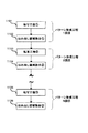
図9に、本実施例におけるインプリント方法のフローについて説明する図を示す。
工程1101は、1回目の転写工程である。
ここでは、基板上に形成した樹脂層に、ステップアンドリピート方式によって、モールドのパターンを転写するインプリントを、1回または複数回行うことにより第1の加工領域を形成する。
また、工程1102は1回目の除去工程である。
ここでは、工程1101で上記第1の加工領域の周囲にはみ出した樹脂によるはみ出し領域を除去する。
これにより、第1回目のパターンが形成される。
このように、本実施例のパターンを形成する工程は、上記したように、転写工程と、転写工程を行った後にはみ出し領域を除去する除去工程と、による一連の工程からなっている。
Since it is difficult to form a pattern on such a
As a result, it is difficult to manufacture a device having a large size by joining the patterns of the mold.
Even when a device having a large size is not manufactured, the protruding
Hereinafter, in the present embodiment, in view of such a problem, an imprint method and a substrate processing method capable of connecting patterns between adjacent processing regions and reducing the manufacturing cost will be described. Do.
FIG. 9 is a diagram for explaining the flow of the imprint method in this embodiment.
Here, the first processing region is formed by performing imprinting for transferring the pattern of the mold once or a plurality of times on the resin layer formed on the substrate by a step-and-repeat method.
Here, in
Thereby, the first pattern is formed.
Thus, as described above, the process of forming the pattern of this embodiment includes a series of processes including the transfer process and the removal process of removing the protruding region after performing the transfer process.
工程1103は、第2の加工領域を形成する2回目の転写工程である。
ここでは工程1102で樹脂層を除去したはみ出し領域上に加工領域が重なるようにインプリント工程を行う。
工程1104は2回目の除去工程である。
ここでは、工程1103で上記第2の加工領域の周囲にはみ出した樹脂によるはみ出し領域を除去する。
これにより、第2回目のパターンが形成される。
Here, the imprint process is performed so that the processing area overlaps the protruding area from which the resin layer has been removed in the
Here, in
Thereby, the second pattern is formed.
このように転写工程と除去工程との一連の工程からなるパターンを形成する工程を、第3回目以降においても複数回繰り返すことで、一旦生じたはみ出し領域上にもパターンを転写することが可能となる。
図9では、1105がN回目の転写工程、1106がN回目の除去工程である。なお、本実施例では、パターン形成工程を3回繰り返し行う場合について説明する。
By repeating the process of forming a pattern consisting of a series of processes including a transfer process and a removal process in this manner a plurality of times even after the third time, it is possible to transfer the pattern onto the protruding region once generated. Become.
In FIG. 9, 1105 is the Nth transfer step, and 1106 is the Nth removal step. In this embodiment, a case where the pattern forming process is repeated three times will be described.
図10(a)は、図2(a)から(e)に示した工程により、1回目の転写工程を行った後の図である。1回目の転写工程で形成された樹脂層401には保護層301(第1の保護層)が設けられており、404は1回目の転写工程におけるはみ出し領域、405は1回目の転写工程における加工領域である。
そして、図10(a)に示すように、基板203上に樹脂層402を形成する。この際に、2回目の転写工程のインプリント工程における加工領域407が、1回目の転写工程におけるはみ出し領域404に重なるようにモールド201および樹脂層402を配置する。
図10(b)に示すように、モールド201を樹脂層402に接触させて、モールド201と基板203の間に樹脂層402を充填させる。
このとき、モールド201により加工領域407から押し出された樹脂層402の一部は、1回目の転写工程における加工領域405の保護層301上にもはみ出す。
図10(c)で、樹脂層を硬化させた後、モールド201を硬化した樹脂層403から剥離することで、モールド201上のパターンが樹脂層403上に転写される。
図10(d)および図10(e)では、1回目の除去工程と同様に、加工領域407の樹脂層403、および加工領域405の樹脂層401を保護層301(第2の保護層)で保護しながら、はみ出し領域406の樹脂層403のみ除去する。
FIG. 10A is a diagram after the first transfer process is performed by the processes shown in FIGS. 2A to 2E. The
Then, as shown in FIG. 10A, a
As shown in FIG. 10B, the
At this time, a part of the
In FIG. 10C, after the resin layer is cured, the pattern on the
10D and 10E, as in the first removal step, the
以上のような工程を行うことにより、もともと樹脂層がはみ出してしまっていて、パターンを転写することができなかった領域にもパターンを転写することが可能となる。
これにより、隣接する加工領域の隙間低減、および隣接する加工領域のパターンをつなげることが可能となる。
ここで一般的には、隙間低減およびパターンをつなげるために、低減またはつなぎの精度と同等の精度をもつモールド201と基板203の位置合わせが必要である。
同様に、3回目のパターン形成工程においても、それ以前の工程におけるはみ出し領域に3回目の加工領域を重ねてパターンを転写し、はみ出し領域の樹脂層のみを除去する。
By performing the steps as described above, it is possible to transfer the pattern even to the region where the resin layer originally protrudes and the pattern cannot be transferred.
As a result, it is possible to reduce the gap between adjacent processing regions and connect patterns of adjacent processing regions.
Here, in general, in order to reduce the gap and connect the patterns, it is necessary to align the
Similarly, in the third pattern formation process, the pattern is transferred by superimposing the third processed area on the protruding area in the previous process, and only the resin layer in the protruding area is removed.
つぎに、パターン形成工程を3回繰り返し行うインプリント方法について具体的に説明する。
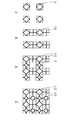
図11に、パターン形成工程を3回繰り返し行うインプリント方法において、各転写工程における加工領域の配置について詳細に説明するために基板を上から見た図を示す。
501は1回目の転写工程における加工領域(第1の加工領域)、502は2回目の転写工程における加工領域(第2の加工領域)、503は3回目の転写工程における加工領域(第3の加工領域)である。
図11(a)に、第1回目のパターンを形成する工程での1回目の転写工程における加工領域(第1の加工領域)の配置を示す。
図における第1方向の配置は、第1方向に対する各加工領域の間隔が、加工領域の第1方向に対する幅の整数倍、例えば2倍となるようにする。
但し、ここにおける加工領域幅の2倍とは、加工領域幅にモールドの加工誤差および基板とモールドの位置合わせ誤差による調整量を加えた長さの2倍とし、以下も同様のものとする。
また、第1方向と直交する第2方向の配置は、第1方向には加工領域幅の1倍の距離動かし、第2方向には例えば加工領域幅の1.5倍の距離動かした位置となるようにする。
但し、第2方向へ動かす距離は、1.5倍に限らず、少なくとも加工領域幅にはみ出し領域の幅を加えた距離であり、大きくても加工領域幅の2倍の長さからはみ出し領域の幅を引いた距離である。
Next, an imprint method in which the pattern forming process is repeated three times will be specifically described.
FIG. 11 shows a top view of the substrate in order to explain in detail the arrangement of the processing regions in each transfer step in the imprint method in which the pattern forming step is repeated three times.
FIG. 11A shows an arrangement of processing regions (first processing regions) in the first transfer process in the first pattern formation process.
The arrangement in the first direction in the drawing is such that the interval between the processing regions with respect to the first direction is an integral multiple of, for example, twice the width of the processing region with respect to the first direction.
However, the double of the processing region width here is twice the length of the processing region width plus the adjustment amount due to the mold processing error and the alignment error between the substrate and the mold, and so on.
Further, the arrangement in the second direction orthogonal to the first direction is a position moved in the first direction by a distance of 1 times the machining area width, and moved in the second direction by a distance of, for example, 1.5 times the machining area width. To be.
However, the distance moved in the second direction is not limited to 1.5 times, and is a distance obtained by adding at least the width of the protruding region to the processing region width. The distance minus the width.
図11(b)に、第2回目のパターンを形成する工程での2回目の転写工程における加工領域502の配置を示す。
図における第1方向に対して、1回目の転写工程における加工領域に隣接するように加工領域を配置する。
図11(c)は、第3回目のパターンを形成する工程での3回目の転写工程における加工領域503の配置を示した図である。
図における第1方向に対して、1回目と2回目の転写工程における加工領域の間に3回目の転写工程における加工領域を配置する。
本実施例のように加工領域を配置することにより、パターン形成工程を3回繰り返すことで基板全域にパターンを転写することができる。
3回以上繰り返す場合においても、前記複数の加工領域における各加工領域の間隔を、前記各加工領域の幅の長さに、前記第1回目のパターンを形成する工程の終了後に、繰り返し行われるパターン形成工程の回数を掛け合わせた長さとすることで、同様に基板全域にパターンを転写することができる。
但し、一般に、パターン形成工程における転写工程と除去工程は、使用する装置を交換する必要があるため、加工方法のスループットを向上させるためには、繰り返し行うパターン形成工程の回数が少ないほうが好ましい。
FIG. 11B shows the arrangement of the
The processing region is arranged adjacent to the processing region in the first transfer process with respect to the first direction in the drawing.
FIG. 11C is a diagram showing the arrangement of the
With respect to the first direction in the figure, the processing region in the third transfer step is arranged between the processing regions in the first and second transfer steps.
By arranging the processing region as in this embodiment, the pattern can be transferred to the entire substrate by repeating the pattern formation step three times.
Even when the process is repeated three or more times, the pattern is repeatedly performed after the step of forming the first pattern with the interval between the process areas in the plurality of process areas set to the width of each process area. By setting the length multiplied by the number of formation steps, the pattern can be similarly transferred to the entire substrate.
However, in general, the transfer process and the removal process in the pattern forming process require replacement of the apparatus to be used. Therefore, in order to improve the throughput of the processing method, it is preferable that the number of repeated pattern forming processes is small.
本実施例のように加工領域を配置することにより、パターン形成工程を3回繰り返すだけで、隣接する全ての加工領域に対して、加工領域間の隙間低減、および加工領域のパターン同士をつなぐことができる。
なお、図11は本実施例の1例を示したに過ぎず、各回の転写工程におけるインプリント工程の回数等は、モールドと基板の大きさや形状により異なる。
By arranging the machining areas as in this embodiment, the pattern formation process is repeated three times, and the gaps between the machining areas are reduced and the patterns of the machining areas are connected to all adjacent machining areas. Can do.
Note that FIG. 11 shows only one example of this embodiment, and the number of imprint processes in each transfer process differs depending on the size and shape of the mold and the substrate.
図12(a)は、図9における工程1106を終えた段階を図11における第1方向の断面として示した図である。
601は1回目の転写工程で形成された樹脂層、602は2回目の転写工程で形成された樹脂層、603は3回目の転写工程で形成された樹脂層である。
図のように1回目の加工領域501と、2回目の加工領域502と、3回目の加工領域503と、さらに別の1回目の加工領域をつなぐことができる。
本実施例では、前述したように各転写工程において、図11における第1方向に対して加工領域の間隔を加工領域幅の2倍にする。
これにより、パターン形成工程を3回繰り返すことで、第1方向に加工領域のパターンをつなげることが可能となる。図12(b)は図12(a)から保護層301のみを除去した状態を示す。保護層301は一連の転写工程および除去工程を行った後除去する。
FIG. 12A is a diagram showing the stage after
As shown in the figure, the
In this embodiment, as described above, in each transfer step, the interval between the processing regions is set to twice the processing region width in the first direction in FIG.
Thereby, it becomes possible to connect the pattern of a process area | region in a 1st direction by repeating a pattern formation process 3 times. FIG. 12B shows a state where only the
以上の工程により、基板203上に所望のパターンが転写された樹脂層を形成することができる。
このように本実施例では、転写工程と除去工程を交互に行い、それを3回ずつ繰り返す。そして、各転写工程における加工領域の配置を図11に示すような配置にすることにより、隣接する全ての加工領域に対して、加工領域間の隙間を低減し、加工領域のパターン同士をつなぐことができる。
また、パターン同士をつなぎあわせない場合にも、製造コストの低減を図ることが可能である。
Through the above steps, a resin layer having a desired pattern transferred onto the
As described above, in this embodiment, the transfer process and the removal process are alternately performed, and the process is repeated three times. Then, by arranging the processing areas in each transfer step as shown in FIG. 11, the gaps between the processing areas are reduced with respect to all the adjacent processing areas, and the patterns of the processing areas are connected. Can do.
Further, even when the patterns are not joined together, it is possible to reduce the manufacturing cost.
また、本実施例において、加工領域の樹脂層の膜厚が均一となり、はみ出し領域の前記基板表面における高さが所定の高さになるように、前記基板上に塗布する樹脂の量および樹脂の分布を制御することが望ましい。
例えば、図10に示すような2回目の転写工程におけるインプリント工程では、はみ出し領域404上に1回目の転写工程で形成された加工領域405の樹脂層401がある。
このため、加工領域407からはみ出される樹脂が影響を受け、加工領域407の樹脂層403の膜厚が大きくなる、またははみ出し領域406の樹脂層による壁の高さが部分的に高くなる場合がある。
このため、2回目の転写工程では、1回目の転写工程よりも塗布する総樹脂量を少なく調整するとよい。
また、1回目の転写工程における加工領域が隣接している箇所の樹脂量が少なくなるように樹脂を分布させるとよい。
このように、はみ出し領域における樹脂層の壁の高さおよび加工領域の樹脂層の膜厚を調整することで、保護層301を加工領域405上のみに形成することができ、また後述する基板へのパターン転写時における転写精度の低下を低減することができる。
Further, in this embodiment, the amount of the resin applied on the substrate and the amount of the resin are adjusted so that the film thickness of the resin layer in the processed region is uniform and the height of the protruding region on the substrate surface is a predetermined height. It is desirable to control the distribution.
For example, in the imprint process in the second transfer process as shown in FIG. 10, there is a
For this reason, the resin protruding from the
For this reason, it is preferable to adjust the total amount of resin applied in the second transfer step to be smaller than that in the first transfer step.
In addition, it is preferable to distribute the resin so that the amount of resin in the portion where the processing regions in the first transfer process are adjacent is small.
As described above, the
また、本実施例においてパターンが転写された樹脂層をマスクとして、基板203にパターンを転写することも可能である。図13にその方法を説明する図を示す。
基板上に転写された樹脂層には、パターンの下地に一般に残膜と呼ばれる厚みが存在する。
図13(a)は樹脂層206の残膜を除去した状態を示す。
図12(b)の状態から、残膜が無くなるまで樹脂層の全面の膜厚を均等に減らすエッチングを行った段階である。次に、残った樹脂層206をマスクとして基板のエッチングを行い図13(b)に示す状態となる。
最後に、残った樹脂層206除去することにより、図13(c)に示すように、基板上に所望のパターンを転写することができる。
なお、本実施例では、基板203へのパターン転写方法は上述した方法のみではなく、他の基板加工方法も取り得る。
例えば、図14は基板203にパターンを転写する別の方法を説明するために示した図である。
1001は反転層である。この方法では、樹脂層の上に、樹脂層とエッチング選択比の取れる材料による反転層を形成する。
反転層に用いる材料としては、前述した保護層と同様の材料を用いることができる。樹脂層の上に反転層を形成すると、図12(a)に示した状態で保護層を反転層として見なした際と同様になる。
前述した保護層を用いたはみ出し領域の樹脂層除去工程を行った際には、樹脂層の上に保護層が形成されている図12(a)の状態から工程を続けることが可能である。この際には保護層を反転層と見なす。
In this embodiment, the pattern can be transferred to the
The resin layer transferred onto the substrate has a thickness generally called a remaining film on the base of the pattern.
FIG. 13A shows a state in which the remaining film of the
From the state of FIG. 12B, etching is performed to uniformly reduce the film thickness of the entire surface of the resin layer until there is no remaining film. Next, the substrate is etched using the remaining
Finally, by removing the remaining
In this embodiment, the pattern transfer method to the
For example, FIG. 14 is a diagram for explaining another method for transferring a pattern to the
As a material used for the inversion layer, the same material as the protective layer described above can be used. When the inversion layer is formed on the resin layer, it is the same as when the protective layer is regarded as the inversion layer in the state shown in FIG.
When the resin layer removal step of the protruding region using the protective layer described above is performed, the process can be continued from the state of FIG. 12A in which the protective layer is formed on the resin layer. In this case, the protective layer is regarded as an inversion layer.
図14(a)は、図12(a)の状態から、樹脂層206の凸部が露出するまで反転層1001の全面を均等にエッチングした状態を示す。
例えば反転層としてSiO2を用いた際には、反転層をエッチングするガス系として、CF4、CHF3、C2F6、C3F8、C4F8、C5F8、C4F6等のフルオロカーボン系をベースとしたものを用いることができる。
次に、樹脂層206の凹部に埋め込まれた反転層1001をマスクに、樹脂層206をエッチングすると図14(b)に示す状態となる。
次に、そのまま反転層1001をマスクに基板もエッチングすると図14(c)に示す状態となる。
最後に残った反転層1001および樹脂層206を除去すると図14(d)に示す状態となり、基板上に所望のパターンを転写することができる。
このような反転層による基板へのパターン転写方法は、樹脂層206自身の全面エッチングにより樹脂層の残膜を除去しないため、パターン上部のエッジ形状を保つことが可能となる。
このことより、樹脂層206をマスクとして基板をエッチングする方法より転写精度を向上させることが可能となる。
FIG. 14A shows a state where the entire surface of the
For example, when SiO 2 is used as the inversion layer, CF 4 , CHF 3 , C 2 F 6 , C 3 F 8 , C 4 F 8 , C 5 F 8 , C 4 are used as gas systems for etching the inversion layer. fluorocarbon such as F 6 can be used which is based.
Next, when the
Next, when the substrate is also etched using the
When the
In such a pattern transfer method to the substrate using the inversion layer, the residual film of the resin layer is not removed by etching the entire surface of the
This makes it possible to improve the transfer accuracy as compared with the method of etching the substrate using the
最後に、本発明における各加工領域のパターンのつなぎについて説明する。例えば、ピッチがXのドットパターンを加工領域205に転写する際に、本発明を用いない場合には図15(a)に示すようになることがある。
すなわち、隣接する加工領域間のはみ出し領域204の幅をYとしたとき、ピッチはY以上となる。ここで、YがXよりも大きい場合等では隣接する加工領域間でピッチをXにすることが難しい。
これに対して本発明を用いることで、図15(b)に示すように、はみ出し領域にもパターンを形成することができ隣接する加工領域同士を近接させることが可能となるため、隣接する加工領域間でドットパターンのピッチをXにすることができる。
このように本実施例では、隣接する加工領域間のパターンをつなぐことが可能となる。このような加工方法は、屈折率の分布が面内方向に周期的に配列されているフォトニック結晶などの構造体に好適に用いることができる。
なお、つなぐことができるパターンとしてはドットパターンに限らず、ラインアンドスペースパターンやホールパターン、及び自由パターン等の他のパターンにも適用可能である。
また、本実施例においてモールドの加工領域の形状は、四角形に限らず、例えば六角形など広く適用可能である。
Finally, the connection of patterns in each processing area in the present invention will be described. For example, when a dot pattern with a pitch of X is transferred to the
That is, when the width of the
On the other hand, by using the present invention, as shown in FIG. 15 (b), it is possible to form a pattern also in the protruding region and to make adjacent processing regions close to each other. The pitch of the dot pattern can be set to X between the regions.
As described above, in this embodiment, it is possible to connect patterns between adjacent processing regions. Such a processing method can be suitably used for a structure such as a photonic crystal in which the refractive index distribution is periodically arranged in the in-plane direction.
The pattern that can be connected is not limited to the dot pattern, but can be applied to other patterns such as a line and space pattern, a hole pattern, and a free pattern.
In the present embodiment, the shape of the processing region of the mold is not limited to a quadrangle, and can be widely applied, for example, a hexagon.
[実施例5]
実施例5においては、実施例4とは別の加工領域の配置方法による構成例について説明する。
実施例4との差異は各回の加工領域の配置方法であるため、その部分についてのみ説明する。
図16を用いて、パターン形成工程に4回繰り返す方法について説明する。
1201は1回目の転写工程における加工領域、1202は2回目の転写工程における加工領域、1203は3回目の転写工程における加工領域、1204は4回目の転写工程における加工領域である。
まず、図16(a)に示すように、1回目の転写工程において、加工領域の並びの周期を第1方向、第2方向共に加工領域幅の2倍として加工領域1201にパターンの転写を行い、その後除去工程を行う。
次に、図16(b)、図16(c)に示すように、2回目の転写工程および3回目の転写工程において、1回目の転写工程における加工領域1201の間の加工領域1202と1203のそれぞれにパターンを転写して、除去工程を行う。
最後に、図16(d)に示すように、残った領域である加工領域1204に4回目の転写工程でパターンを転写して除去工程を行う。パターン形成工程を3回繰り返す方法では、加工領域の配置において、第1方向または第2方向のどちらか一方向は加工領域の端を揃えることはできない。
これに対して、パターン形成工程を4回繰り返す方法では、第1方向と第2方向の両方で加工領域の端を揃えることが可能となる。
つまり、網の目上に加工領域の端をダイシングする場合等、第1方向と第2方向の両方で加工領域の端を揃える必要がある場合においても、それぞれの加工領域のパターンをつないでパターンを転写することが可能である。
[Example 5]
In the fifth embodiment, a configuration example based on a method of arranging a processing region different from that of the fourth embodiment will be described.
Since the difference from the fourth embodiment is the method of arranging the processing regions each time, only that portion will be described.
A method of repeating the pattern forming process four times will be described with reference to FIG.
First, as shown in FIG. 16A, in the first transfer process, the pattern is transferred to the
Next, as shown in FIG. 16B and FIG. 16C, in the second transfer step and the third transfer step, the
Finally, as shown in FIG. 16D, the removal process is performed by transferring the pattern to the
On the other hand, in the method of repeating the pattern formation process four times, it is possible to align the edges of the processing region in both the first direction and the second direction.
In other words, even when it is necessary to align the edges of the machining area in both the first direction and the second direction, such as when dicing the edge of the machining area on a mesh, the pattern of each machining area is connected. Can be transferred.
図17を用いて、パターン形成工程を2回繰り返す方法について説明する。
図17(a)に示すように、1回目の転写工程において、第1方向加工領域の並びの周期を加工領域の幅の2倍とし、第2方向の間隔は適当な幅としてパターンの転写を行い、除去工程を行う。
ここにおける適当な幅とは、各インプリント工程におけるはみ出し領域が隣接する加工領域に重ならない幅とする。
次に、図17(b)に示すように2回目の転写工程において、1回目の転写工程における第1方向の加工領域の間にパターンを転写してそれぞれ除去工程を行う。
以上の工程によって、一方向にのみ各加工領域の転写パターンをつなぐ必要がある場合においては、パターン形成工程をそれぞれ3回よりも少ない2回だけ繰り返すことでパターンを転写することが可能となる。
なお、本発明における、パターン形成工程の回数、または加工領域の配置方法、配置の順番、またはモールドの加工領域の形状は、これだけに限るものではない。
A method of repeating the pattern forming process twice will be described with reference to FIG.
As shown in FIG. 17 (a), in the first transfer process, the period of the arrangement of the first direction processed areas is set to twice the width of the processed areas, and the interval in the second direction is set to an appropriate width to transfer the pattern. And removing step.
The appropriate width here is a width in which the protruding region in each imprint process does not overlap with the adjacent processing region.
Next, as shown in FIG. 17B, in the second transfer process, the pattern is transferred between the processing regions in the first direction in the first transfer process, and the removal process is performed.
When it is necessary to connect the transfer patterns of the respective processing regions only in one direction by the above steps, the pattern can be transferred by repeating the pattern forming step only twice less than three times.
In the present invention, the number of pattern forming steps, the arrangement method of the processing areas, the order of arrangement, or the shape of the processing area of the mold is not limited to this.
[実施例6]
実施例6における実施例4と実施例5との差異は、各転写工程に用いるモールドの構成であるため、その部分についてのみ説明する。
本発明では、各転写工程に同じモールドを用いるとは限らない。つまり、例えば実施例2におけるパターン形成工程を4回繰り返す方法において、1回目、2回目、3回目、4回目の転写工程にそれぞれ異なるモールドを用いることも可能である。
[Example 6]
Since the difference between Example 4 and Example 5 in Example 6 is the configuration of the mold used in each transfer step, only that part will be described.
In the present invention, the same mold is not necessarily used for each transfer step. That is, for example, in the method of repeating the pattern forming process in Example 2 four times, it is possible to use different molds for the first, second, third and fourth transfer processes.
図18(a)は1回目のパターン形成工程を終えた段階を示す。
図18(b)は2回目のパターン形成工程を終えた段階を示す。
ここで、2回目の転写工程に用いたモールドは、1回目の転写工程に用いたモールドとは異なるパターンを持ったモールドである。
図18(c)は3回目のパターン形成工程を終えた段階を示す。3回目の転写工程で用いたモールドは、1回目と2回目とは異なるパターンをもつモールドであり、このモールドを用いて転写工程を行う。
図18(d)は4回目のパターン形成工程終えた段階を示す。4回目の転写工程で用いたモールドも、1回目、2回目、3回目とは異なるパターンをもつモールドであり、このモールドを用いて転写工程を行う。
全ての転写工程に同じパターンをもつモールドを用いた際には、大きくても1つの加工領域分の周期をもつパターンしか転写できない。
しかし、このように各回の転写工程に異なるパターンをもつモールドを用いることで、4倍の周期構造をもつパターンを転写することが可能となる。
FIG. 18A shows a stage where the first pattern formation process is completed.
FIG. 18B shows a stage where the second pattern formation process is completed.
Here, the mold used in the second transfer process is a mold having a different pattern from the mold used in the first transfer process.
FIG. 18C shows a stage where the third pattern formation process is completed. The mold used in the third transfer process is a mold having a pattern different from the first and second processes, and the transfer process is performed using this mold.
FIG. 18D shows a stage after the fourth pattern formation process. The mold used in the fourth transfer process is also a mold having a different pattern from the first, second, and third times, and the transfer process is performed using this mold.
When a mold having the same pattern is used for all transfer processes, only a pattern having a period corresponding to one processing region can be transferred at most.
However, by using a mold having a different pattern for each transfer step in this way, a pattern having a fourfold periodic structure can be transferred.
以上のように、本実施例では、各回の転写工程にパターンの異なるモールドを用いることで、より大きな周期を持つパターンを転写することが可能となる。 As described above, in this embodiment, it is possible to transfer a pattern having a larger cycle by using a mold having a different pattern for each transfer process.
101:インプリント工程
102:保護層形成工程
103:はみ出し領域除去工程
104:基板加工工程
201:モールド
202:インプリント層
203:基板
204:はみ出し領域
205:パターン形成領域
301:保護層
401:硬化した1回目の樹脂層
402:2回目の樹脂層
403:硬化した2回目の樹脂層
404:1回目のはみ出し領域
405:1回目の加工領域
406:2回目のはみ出し領域
407:2回目の加工領域
501:1回目の加工領域
502:2回目の加工領域
503:3回目の加工領域
601:1回目の樹脂層
602:2回目の樹脂層
603:3回目の樹脂層
1001:反転層
1201:1回目の加工領域
1202:2回目の加工領域
1203:3回目の加工領域
1204:4回目の加工領域
t1:インプリント層の残膜膜厚
t2:インプリント層のパターン高さ
t3:保護層の膜厚
t4:はみ出し領域におけるインプリント層の高さ
d1:パターン形成領域の幅
d2:はみ出し領域の幅
101: imprint process 102: protective layer forming process 103: protruding area removing process 104: substrate processing process 201: mold 202: imprint layer 203: substrate 204: protruding area 205: pattern forming area 301: protective layer 401: cured First resin layer 402: Second resin layer 403: Cured second resin layer 404: First protrusion region 405: First processing region 406: Second protrusion region 407:
Claims (7)
第1回目のパターンを形成する工程と、
第2回目のパターンを形成する工程と、を有し、
前記第1回目のパターンを形成する工程は、
前記基板上に形成された樹脂に、前記モールドを接触させ、該モールドのパターンに対応する凹凸パターンを形成した第1の加工領域と、該第1の加工領域の周囲に前記樹脂によるはみ出し領域を形成する工程と、
前記第1の加工領域の上に、該第1の加工領域を保護する第1の保護層を形成する工程と、
前記第1の保護層によって、前記第1の加工領域の樹脂層に形成されたパターンが除去されないように保護しながら、前記はみ出し領域の樹脂層を除去する工程と、
を有し、
前記第2回目のパターンを形成する工程は、
前記はみ出し領域を含む前記第1の加工領域と隣接する領域に形成された樹脂に前記モールドを接触させ、第2の加工領域を形成する工程と、
前記第2の加工領域の樹脂層に、該第2の加工領域を保護する第2の保護層を形成する工程と、
前記第1及び第2の保護層によって、前記第1及び第2の加工領域の樹脂層に形成されたパターンが除去されないように保護しながら、前記第2の加工領域の周囲にはみ出した樹脂を除去する工程と、
を有することを特徴とするインプリント方法。 A process of imprinting a pattern of a mold on a resin on a substrate to form a pattern is an imprint method that is repeated a plurality of times,
Forming a first pattern;
Forming a second pattern, and
The step of forming the first pattern includes:
The mold is brought into contact with the resin formed on the substrate to form a first processing region in which a concavo-convex pattern corresponding to the pattern of the mold is formed, and a protrusion region by the resin around the first processing region. Forming, and
Forming a first protective layer for protecting the first processing region on the first processing region;
Removing the resin layer in the protruding region while protecting the pattern formed on the resin layer in the first processing region from being removed by the first protective layer;
Have
The step of forming the second pattern includes:
Contacting the mold with a resin formed in a region adjacent to the first processing region including the protruding region to form a second processing region;
Forming a second protective layer for protecting the second processing region on the resin layer of the second processing region;
While the first and second protective layers protect the pattern formed on the resin layers in the first and second processed regions from being removed, the resin that protrudes around the second processed region is removed. Removing, and
The imprint method characterized by having.
前記複数の加工領域における各加工領域の間隔を、前記加工領域の幅の長さの整数倍とすることを特徴とする請求項1に記載のインプリント方法。 In the step of forming the first pattern, when forming a plurality of processing regions in the first processing region in at least one of the first direction or the second direction orthogonal to the first direction,
Imprinting method of claim 1, wherein the plurality of the intervals between the machining area in the processing region, an integral multiple of the length of the width of the working area.
前記第2回目のパターンを形成する工程の後に、前記第2の加工領域と隣接する領域に第3の加工領域を形成する工程と、
を有することを特徴とする請求項2に記載のインプリント方法。 In the imprint method in which the step of forming the pattern is repeated three times, an interval between the processing regions formed in the first direction in the first processing region is set to a length of the width of the first processing region. A step of forming each of the processing regions, with the processing regions in the second direction being spaced apart from each other,
After the step of forming the second pattern, forming a third processing region in a region adjacent to the second processing region;
The imprint method according to claim 2 , further comprising:
Priority Applications (6)
| Application Number | Priority Date | Filing Date | Title |
|---|---|---|---|
| JP2008182297A JP5473266B2 (en) | 2007-08-03 | 2008-07-14 | Imprint method, substrate processing method, and semiconductor device manufacturing method by substrate processing method |
| US12/282,454 US8361336B2 (en) | 2007-08-03 | 2008-08-01 | Imprint method for imprinting a pattern of a mold onto a resin material of a substrate and related substrate processing method |
| PCT/JP2008/064265 WO2009020196A1 (en) | 2007-08-03 | 2008-08-01 | Imprint method and processing method of substrate using the imprint method |
| CN2008801009858A CN101765809B (en) | 2007-08-03 | 2008-08-01 | Imprint method and processing method of substrate using the imprint method |
| EP08792322A EP2176709B1 (en) | 2007-08-03 | 2008-08-01 | Imprint method and processing method of substrate using the imprint method |
| KR1020107003787A KR101155200B1 (en) | 2007-08-03 | 2008-08-01 | Imprint method and processing method of substrate using the imprint method |
Applications Claiming Priority (5)
| Application Number | Priority Date | Filing Date | Title |
|---|---|---|---|
| JP2007203050 | 2007-08-03 | ||
| JP2007203044 | 2007-08-03 | ||
| JP2007203044 | 2007-08-03 | ||
| JP2007203050 | 2007-08-03 | ||
| JP2008182297A JP5473266B2 (en) | 2007-08-03 | 2008-07-14 | Imprint method, substrate processing method, and semiconductor device manufacturing method by substrate processing method |
Publications (3)
| Publication Number | Publication Date |
|---|---|
| JP2009060084A JP2009060084A (en) | 2009-03-19 |
| JP2009060084A5 JP2009060084A5 (en) | 2011-08-11 |
| JP5473266B2 true JP5473266B2 (en) | 2014-04-16 |
Family
ID=39865438
Family Applications (1)
| Application Number | Title | Priority Date | Filing Date |
|---|---|---|---|
| JP2008182297A Expired - Fee Related JP5473266B2 (en) | 2007-08-03 | 2008-07-14 | Imprint method, substrate processing method, and semiconductor device manufacturing method by substrate processing method |
Country Status (6)
| Country | Link |
|---|---|
| US (1) | US8361336B2 (en) |
| EP (1) | EP2176709B1 (en) |
| JP (1) | JP5473266B2 (en) |
| KR (1) | KR101155200B1 (en) |
| CN (1) | CN101765809B (en) |
| WO (1) | WO2009020196A1 (en) |
Families Citing this family (26)
| Publication number | Priority date | Publication date | Assignee | Title |
|---|---|---|---|---|
| JP5258635B2 (en) * | 2008-03-18 | 2013-08-07 | キヤノン株式会社 | Nanoimprint method, mold used for nanoimprint, and method for producing structure |
| GB2468635B (en) * | 2009-02-05 | 2014-05-14 | Api Group Plc | Production of a surface relief on a substrate |
| US20110031650A1 (en) * | 2009-08-04 | 2011-02-10 | Molecular Imprints, Inc. | Adjacent Field Alignment |
| EP2463073B1 (en) * | 2009-08-07 | 2018-04-04 | Soken Chemical & Engineering Co., Ltd. | Resin mold for imprinting and method for producing same |
| JP4963718B2 (en) * | 2009-10-23 | 2012-06-27 | キヤノン株式会社 | Imprint method, imprint apparatus, and article manufacturing method using the same |
| JP5546893B2 (en) | 2010-02-16 | 2014-07-09 | 東京エレクトロン株式会社 | Imprint method |
| JP5850717B2 (en) | 2010-12-02 | 2016-02-03 | キヤノン株式会社 | Imprint apparatus and article manufacturing method using the same |
| JP5558327B2 (en) | 2010-12-10 | 2014-07-23 | 株式会社東芝 | Pattern forming method, semiconductor device manufacturing method, and template manufacturing method |
| JP5863286B2 (en) * | 2011-06-16 | 2016-02-16 | キヤノン株式会社 | Imprint method, imprint apparatus, and article manufacturing method |
| JP6056294B2 (en) * | 2011-09-28 | 2017-01-11 | 大日本印刷株式会社 | Pattern formation method |
| SG10201608504SA (en) | 2011-12-19 | 2016-12-29 | Canon Nanotechnologies Inc | Fabrication of seamless large area master templates for imprint lithography |
| CN105358979A (en) * | 2013-03-15 | 2016-02-24 | 普林斯顿大学理事会 | Analyte detection enhancement by targeted immobilization, surface amplification, and pixelated reading and analysis |
| JP2015028978A (en) * | 2013-07-30 | 2015-02-12 | 大日本印刷株式会社 | Foreign matter detection method, imprint method, and imprint system |
| WO2016065308A1 (en) * | 2014-10-23 | 2016-04-28 | Board Of Regents, The University Of Texas System | Nanoshape patterning techniques that allow high-speed and low-cost fabrication of nanoshape structures |
| DE102015118991A1 (en) * | 2015-11-05 | 2017-05-11 | Ev Group E. Thallner Gmbh | Method of treating millimeter and / or micrometer and / or nanometer structures on a surface of a substrate |
| JP6655988B2 (en) * | 2015-12-25 | 2020-03-04 | キヤノン株式会社 | Adjustment method of imprint apparatus, imprint method, and article manufacturing method |
| KR102535820B1 (en) * | 2016-05-19 | 2023-05-24 | 삼성디스플레이 주식회사 | Imprint lithograhy method, substrate manufactured by the method, master template for imprint, wire grid polarizer manufactured using the master template and display substrate having the same |
| KR20180009825A (en) * | 2016-07-19 | 2018-01-30 | 삼성디스플레이 주식회사 | Roll type imprint master mold, manufacturing the same, and imprint method using the same |
| CA3037145A1 (en) * | 2016-09-27 | 2018-04-05 | Illumina, Inc. | Imprinted substrates |
| KR20180039228A (en) | 2016-10-07 | 2018-04-18 | 삼성디스플레이 주식회사 | Method of manufacturing display apparatus |
| JP7425602B2 (en) * | 2017-03-08 | 2024-01-31 | キヤノン株式会社 | Pattern forming method, method for manufacturing processed substrates, optical components and quartz mold replicas, imprint pre-treatment coating material and set thereof with imprint resist |
| US11366400B2 (en) * | 2017-05-15 | 2022-06-21 | Canon Kabushiki Kaisha | Method of determining drop recipe, imprint apparatus, and article manufacturing method |
| TWI646389B (en) | 2017-09-12 | 2019-01-01 | 友達光電股份有限公司 | Imprinting mold and manufacturing method of imprinting mold |
| KR20200026407A (en) | 2018-08-31 | 2020-03-11 | 삼성디스플레이 주식회사 | Master stamp for nano imprint and method of manufacturing of the smae |
| CN109188863B (en) * | 2018-11-05 | 2021-11-26 | 京东方科技集团股份有限公司 | Method for patterning film layer |
| CN110764364B (en) * | 2019-11-01 | 2021-05-25 | 京东方科技集团股份有限公司 | Manufacturing method of nano pattern, nano imprinting substrate and display substrate |
Family Cites Families (19)
| Publication number | Priority date | Publication date | Assignee | Title |
|---|---|---|---|---|
| JP2000194142A (en) | 1998-12-25 | 2000-07-14 | Fujitsu Ltd | Pattern forming method and production of semiconductor device |
| US6334960B1 (en) | 1999-03-11 | 2002-01-01 | Board Of Regents, The University Of Texas System | Step and flash imprint lithography |
| US6932934B2 (en) * | 2002-07-11 | 2005-08-23 | Molecular Imprints, Inc. | Formation of discontinuous films during an imprint lithography process |
| JP4002154B2 (en) * | 2002-08-13 | 2007-10-31 | 東芝松下ディスプレイテクノロジー株式会社 | Method and apparatus for manufacturing liquid crystal display element |
| US7396475B2 (en) * | 2003-04-25 | 2008-07-08 | Molecular Imprints, Inc. | Method of forming stepped structures employing imprint lithography |
| JP4190371B2 (en) * | 2003-08-26 | 2008-12-03 | Tdk株式会社 | Uneven pattern forming stamper, uneven pattern forming method, and magnetic recording medium |
| US7435074B2 (en) * | 2004-03-13 | 2008-10-14 | International Business Machines Corporation | Method for fabricating dual damascence structures using photo-imprint lithography, methods for fabricating imprint lithography molds for dual damascene structures, materials for imprintable dielectrics and equipment for photo-imprint lithography used in dual damascence patterning |
| US7241395B2 (en) | 2004-09-21 | 2007-07-10 | Molecular Imprints, Inc. | Reverse tone patterning on surfaces having planarity perturbations |
| US7490547B2 (en) * | 2004-12-30 | 2009-02-17 | Asml Netherlands B.V. | Imprint lithography |
| US20060177532A1 (en) * | 2005-02-04 | 2006-08-10 | Molecular Imprints, Inc. | Imprint lithography method to control extrusion of a liquid from a desired region on a substrate |
| US8999218B2 (en) | 2005-06-06 | 2015-04-07 | Canon Kabushiki Kaisha | Process for producing member having pattern, pattern transfer apparatus, and mold |
| JP3958344B2 (en) | 2005-06-07 | 2007-08-15 | キヤノン株式会社 | Imprint apparatus, imprint method, and chip manufacturing method |
| US7927089B2 (en) | 2005-06-08 | 2011-04-19 | Canon Kabushiki Kaisha | Mold, apparatus including mold, pattern transfer apparatus, and pattern forming method |
| CN1928711B (en) * | 2005-09-06 | 2010-05-12 | 佳能株式会社 | Mold, imprint method, and process for producing chip |
| US8011916B2 (en) * | 2005-09-06 | 2011-09-06 | Canon Kabushiki Kaisha | Mold, imprint apparatus, and process for producing structure |
| JP4630795B2 (en) * | 2005-10-26 | 2011-02-09 | 株式会社東芝 | Pattern forming method and method for manufacturing magnetic recording medium |
| JP4736821B2 (en) * | 2006-01-24 | 2011-07-27 | 株式会社日立製作所 | Pattern forming method and pattern forming apparatus |
| JP4861044B2 (en) * | 2006-04-18 | 2012-01-25 | キヤノン株式会社 | Substrate processing method and method for manufacturing member having pattern region |
| KR20070105040A (en) * | 2006-04-25 | 2007-10-30 | 엘지.필립스 엘시디 주식회사 | Resist composition, method of fabricating resist pattern using the same and array substrate fabricated using the same |
-
2008
- 2008-07-14 JP JP2008182297A patent/JP5473266B2/en not_active Expired - Fee Related
- 2008-08-01 US US12/282,454 patent/US8361336B2/en not_active Expired - Fee Related
- 2008-08-01 EP EP08792322A patent/EP2176709B1/en not_active Not-in-force
- 2008-08-01 WO PCT/JP2008/064265 patent/WO2009020196A1/en active Application Filing
- 2008-08-01 CN CN2008801009858A patent/CN101765809B/en not_active Expired - Fee Related
- 2008-08-01 KR KR1020107003787A patent/KR101155200B1/en active IP Right Grant
Also Published As
| Publication number | Publication date |
|---|---|
| US20110042352A1 (en) | 2011-02-24 |
| JP2009060084A (en) | 2009-03-19 |
| EP2176709A1 (en) | 2010-04-21 |
| US8361336B2 (en) | 2013-01-29 |
| CN101765809B (en) | 2012-05-16 |
| CN101765809A (en) | 2010-06-30 |
| EP2176709B1 (en) | 2012-07-18 |
| KR101155200B1 (en) | 2012-06-13 |
| WO2009020196A1 (en) | 2009-02-12 |
| KR20100047268A (en) | 2010-05-07 |
Similar Documents
| Publication | Publication Date | Title |
|---|---|---|
| JP5473266B2 (en) | Imprint method, substrate processing method, and semiconductor device manufacturing method by substrate processing method | |
| JP5197342B2 (en) | Substrate processing method by imprint | |
| JP5274128B2 (en) | Imprint method and substrate processing method | |
| US7960090B2 (en) | Pattern forming method, pattern formed thereby, mold, processing apparatus, and processing method | |
| JP5377053B2 (en) | Template, manufacturing method thereof, and pattern forming method | |
| JP2009182075A (en) | Manufacturing method of structure by imprint | |
| TWI391986B (en) | Imprinting of partial fields at the edge of the wafer | |
| US7815430B2 (en) | Mold, production process of mold, imprint apparatus, and imprint method | |
| US7854604B2 (en) | Semiconductor device fabrication method and pattern formation mold | |
| US8178026B2 (en) | Nanoimprinting method and mold for use in nanoimprinting | |
| US20150017329A1 (en) | Drop pattern generation for imprint lithography with directionally-patterned templates | |
| US20110111593A1 (en) | Pattern formation method, pattern formation system, and method for manufacturing semiconductor device | |
| JP2009053271A (en) | Method for forming mold, method for forming diffraction grating and method for manufacturing distributed feedback type semiconductor laser | |
| JP6232731B2 (en) | Manufacturing method of imprint mold | |
| KR20100035130A (en) | Imprinting method | |
| JP4861044B2 (en) | Substrate processing method and method for manufacturing member having pattern region | |
| US20120241409A1 (en) | Pattern formation method | |
| JP6136721B2 (en) | Pattern forming method and imprint mold manufacturing method | |
| JP2010264720A (en) | Nanoimprint mold and method of manufacturing semiconductor optical device using the same | |
| JP6163840B2 (en) | Manufacturing method of fine pattern formed body | |
| US20210373217A1 (en) | Fine pattern forming method, imprint mold manufacturing method, imprint mold, and optical device | |
| JP2024001577A (en) | Template, pattern forming method, and semiconductor device manufacturing method |
Legal Events
| Date | Code | Title | Description |
|---|---|---|---|
| A521 | Written amendment |
Free format text: JAPANESE INTERMEDIATE CODE: A523 Effective date: 20110624 |
|
| A621 | Written request for application examination |
Free format text: JAPANESE INTERMEDIATE CODE: A621 Effective date: 20110624 |
|
| A131 | Notification of reasons for refusal |
Free format text: JAPANESE INTERMEDIATE CODE: A131 Effective date: 20130416 |
|
| A521 | Written amendment |
Free format text: JAPANESE INTERMEDIATE CODE: A523 Effective date: 20130614 |
|
| RD01 | Notification of change of attorney |
Free format text: JAPANESE INTERMEDIATE CODE: A7421 Effective date: 20131212 |
|
| TRDD | Decision of grant or rejection written | ||
| A01 | Written decision to grant a patent or to grant a registration (utility model) |
Free format text: JAPANESE INTERMEDIATE CODE: A01 Effective date: 20140107 |
|
| A61 | First payment of annual fees (during grant procedure) |
Free format text: JAPANESE INTERMEDIATE CODE: A61 Effective date: 20140204 |
|
| R151 | Written notification of patent or utility model registration |
Ref document number: 5473266 Country of ref document: JP Free format text: JAPANESE INTERMEDIATE CODE: R151 |
|
| LAPS | Cancellation because of no payment of annual fees |