JP5847184B2 - 浸漬低インダクタンスrfコイル及びマルチカスプ磁気配列を用いた誘導結合型プラズマフラッドガン - Google Patents
浸漬低インダクタンスrfコイル及びマルチカスプ磁気配列を用いた誘導結合型プラズマフラッドガン Download PDFInfo
- Publication number
- JP5847184B2 JP5847184B2 JP2013532983A JP2013532983A JP5847184B2 JP 5847184 B2 JP5847184 B2 JP 5847184B2 JP 2013532983 A JP2013532983 A JP 2013532983A JP 2013532983 A JP2013532983 A JP 2013532983A JP 5847184 B2 JP5847184 B2 JP 5847184B2
- Authority
- JP
- Japan
- Prior art keywords
- plasma
- magnets
- coil
- plasma chamber
- pair
- Prior art date
- Legal status (The legal status is an assumption and is not a legal conclusion. Google has not performed a legal analysis and makes no representation as to the accuracy of the status listed.)
- Active
Links
- 238000009616 inductively coupled plasma Methods 0.000 title 1
- 238000000034 method Methods 0.000 claims description 18
- 238000005468 ion implantation Methods 0.000 claims description 16
- 239000000463 material Substances 0.000 claims description 13
- 229910052751 metal Inorganic materials 0.000 claims description 12
- 239000002184 metal Substances 0.000 claims description 12
- 239000002245 particle Substances 0.000 claims description 7
- 239000000126 substance Substances 0.000 claims description 7
- OKTJSMMVPCPJKN-UHFFFAOYSA-N Carbon Chemical compound [C] OKTJSMMVPCPJKN-UHFFFAOYSA-N 0.000 claims description 6
- 229910002804 graphite Inorganic materials 0.000 claims description 6
- 239000010439 graphite Substances 0.000 claims description 6
- 239000010453 quartz Substances 0.000 claims description 5
- VYPSYNLAJGMNEJ-UHFFFAOYSA-N silicon dioxide Inorganic materials O=[Si]=O VYPSYNLAJGMNEJ-UHFFFAOYSA-N 0.000 claims description 5
- HBMJWWWQQXIZIP-UHFFFAOYSA-N silicon carbide Chemical compound [Si+]#[C-] HBMJWWWQQXIZIP-UHFFFAOYSA-N 0.000 claims description 4
- 230000008878 coupling Effects 0.000 claims description 3
- 238000010168 coupling process Methods 0.000 claims description 3
- 238000005859 coupling reaction Methods 0.000 claims description 3
- 150000002736 metal compounds Chemical class 0.000 claims description 3
- 229910010271 silicon carbide Inorganic materials 0.000 claims description 3
- 238000010884 ion-beam technique Methods 0.000 description 31
- 150000002500 ions Chemical class 0.000 description 30
- 239000000758 substrate Substances 0.000 description 20
- 239000007789 gas Substances 0.000 description 14
- XKRFYHLGVUSROY-UHFFFAOYSA-N Argon Chemical compound [Ar] XKRFYHLGVUSROY-UHFFFAOYSA-N 0.000 description 6
- 238000011109 contamination Methods 0.000 description 5
- 229910052724 xenon Inorganic materials 0.000 description 5
- FHNFHKCVQCLJFQ-UHFFFAOYSA-N xenon atom Chemical compound [Xe] FHNFHKCVQCLJFQ-UHFFFAOYSA-N 0.000 description 5
- 229910052782 aluminium Inorganic materials 0.000 description 4
- XAGFODPZIPBFFR-UHFFFAOYSA-N aluminium Chemical compound [Al] XAGFODPZIPBFFR-UHFFFAOYSA-N 0.000 description 4
- 239000004020 conductor Substances 0.000 description 4
- 238000007654 immersion Methods 0.000 description 4
- 238000002513 implantation Methods 0.000 description 4
- 238000009825 accumulation Methods 0.000 description 3
- 229910052786 argon Inorganic materials 0.000 description 3
- 230000008859 change Effects 0.000 description 3
- 230000006870 function Effects 0.000 description 3
- 239000011261 inert gas Substances 0.000 description 3
- 229910052743 krypton Inorganic materials 0.000 description 3
- DNNSSWSSYDEUBZ-UHFFFAOYSA-N krypton atom Chemical compound [Kr] DNNSSWSSYDEUBZ-UHFFFAOYSA-N 0.000 description 3
- 230000008569 process Effects 0.000 description 3
- 238000001472 pulsed field gradient Methods 0.000 description 3
- 239000004065 semiconductor Substances 0.000 description 3
- 238000003860 storage Methods 0.000 description 3
- WFKWXMTUELFFGS-UHFFFAOYSA-N tungsten Chemical compound [W] WFKWXMTUELFFGS-UHFFFAOYSA-N 0.000 description 3
- 230000005591 charge neutralization Effects 0.000 description 2
- 239000011248 coating agent Substances 0.000 description 2
- 238000000576 coating method Methods 0.000 description 2
- 239000000356 contaminant Substances 0.000 description 2
- 239000002019 doping agent Substances 0.000 description 2
- 230000005684 electric field Effects 0.000 description 2
- 238000000605 extraction Methods 0.000 description 2
- 230000006698 induction Effects 0.000 description 2
- 230000004048 modification Effects 0.000 description 2
- 238000012986 modification Methods 0.000 description 2
- 230000009467 reduction Effects 0.000 description 2
- 239000003507 refrigerant Substances 0.000 description 2
- 229910052721 tungsten Inorganic materials 0.000 description 2
- 239000010937 tungsten Substances 0.000 description 2
- 229910018072 Al 2 O 3 Inorganic materials 0.000 description 1
- RYGMFSIKBFXOCR-UHFFFAOYSA-N Copper Chemical compound [Cu] RYGMFSIKBFXOCR-UHFFFAOYSA-N 0.000 description 1
- 230000001133 acceleration Effects 0.000 description 1
- 230000009471 action Effects 0.000 description 1
- 230000002411 adverse Effects 0.000 description 1
- 239000000919 ceramic Substances 0.000 description 1
- 150000001793 charged compounds Chemical class 0.000 description 1
- 229910052802 copper Inorganic materials 0.000 description 1
- 239000010949 copper Substances 0.000 description 1
- 230000007812 deficiency Effects 0.000 description 1
- 230000006866 deterioration Effects 0.000 description 1
- 239000003989 dielectric material Substances 0.000 description 1
- 230000002708 enhancing effect Effects 0.000 description 1
- 238000010438 heat treatment Methods 0.000 description 1
- 239000012535 impurity Substances 0.000 description 1
- 230000001939 inductive effect Effects 0.000 description 1
- 238000004519 manufacturing process Methods 0.000 description 1
- 229910021645 metal ion Inorganic materials 0.000 description 1
- 150000002739 metals Chemical class 0.000 description 1
- 230000003472 neutralizing effect Effects 0.000 description 1
- 229910052755 nonmetal Inorganic materials 0.000 description 1
- TWNQGVIAIRXVLR-UHFFFAOYSA-N oxo(oxoalumanyloxy)alumane Chemical compound O=[Al]O[Al]=O TWNQGVIAIRXVLR-UHFFFAOYSA-N 0.000 description 1
- 230000001681 protective effect Effects 0.000 description 1
- 230000002459 sustained effect Effects 0.000 description 1
- 210000003813 thumb Anatomy 0.000 description 1
- 238000011144 upstream manufacturing Methods 0.000 description 1
- XLYOFNOQVPJJNP-UHFFFAOYSA-N water Substances O XLYOFNOQVPJJNP-UHFFFAOYSA-N 0.000 description 1
Images


Classifications
-
- H—ELECTRICITY
- H01—ELECTRIC ELEMENTS
- H01J—ELECTRIC DISCHARGE TUBES OR DISCHARGE LAMPS
- H01J37/00—Discharge tubes with provision for introducing objects or material to be exposed to the discharge, e.g. for the purpose of examination or processing thereof
- H01J37/02—Details
- H01J37/026—Means for avoiding or neutralising unwanted electrical charges on tube components
-
- H—ELECTRICITY
- H01—ELECTRIC ELEMENTS
- H01J—ELECTRIC DISCHARGE TUBES OR DISCHARGE LAMPS
- H01J37/00—Discharge tubes with provision for introducing objects or material to be exposed to the discharge, e.g. for the purpose of examination or processing thereof
- H01J37/30—Electron-beam or ion-beam tubes for localised treatment of objects
- H01J37/317—Electron-beam or ion-beam tubes for localised treatment of objects for changing properties of the objects or for applying thin layers thereon, e.g. for ion implantation
- H01J37/3171—Electron-beam or ion-beam tubes for localised treatment of objects for changing properties of the objects or for applying thin layers thereon, e.g. for ion implantation for ion implantation
-
- H—ELECTRICITY
- H01—ELECTRIC ELEMENTS
- H01J—ELECTRIC DISCHARGE TUBES OR DISCHARGE LAMPS
- H01J37/00—Discharge tubes with provision for introducing objects or material to be exposed to the discharge, e.g. for the purpose of examination or processing thereof
- H01J37/32—Gas-filled discharge tubes
- H01J37/32009—Arrangements for generation of plasma specially adapted for examination or treatment of objects, e.g. plasma sources
- H01J37/32082—Radio frequency generated discharge
- H01J37/321—Radio frequency generated discharge the radio frequency energy being inductively coupled to the plasma
- H01J37/3211—Antennas, e.g. particular shapes of coils
-
- H—ELECTRICITY
- H01—ELECTRIC ELEMENTS
- H01J—ELECTRIC DISCHARGE TUBES OR DISCHARGE LAMPS
- H01J37/00—Discharge tubes with provision for introducing objects or material to be exposed to the discharge, e.g. for the purpose of examination or processing thereof
- H01J37/32—Gas-filled discharge tubes
- H01J37/32431—Constructional details of the reactor
- H01J37/3266—Magnetic control means
- H01J37/32688—Multi-cusp fields
-
- H—ELECTRICITY
- H01—ELECTRIC ELEMENTS
- H01J—ELECTRIC DISCHARGE TUBES OR DISCHARGE LAMPS
- H01J2237/00—Discharge tubes exposing object to beam, e.g. for analysis treatment, etching, imaging
- H01J2237/03—Mounting, supporting, spacing or insulating electrodes
-
- H—ELECTRICITY
- H01—ELECTRIC ELEMENTS
- H01J—ELECTRIC DISCHARGE TUBES OR DISCHARGE LAMPS
- H01J2237/00—Discharge tubes exposing object to beam, e.g. for analysis treatment, etching, imaging
- H01J2237/03—Mounting, supporting, spacing or insulating electrodes
- H01J2237/032—Mounting or supporting
Landscapes
- Chemical & Material Sciences (AREA)
- Analytical Chemistry (AREA)
- Physics & Mathematics (AREA)
- Engineering & Computer Science (AREA)
- Plasma & Fusion (AREA)
- Electron Sources, Ion Sources (AREA)
- Plasma Technology (AREA)
Description
発明の分野
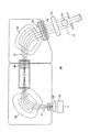
本発明の実施形態は、半導体構造のイオン注入の分野に関するものである。特に、本発明は、低エネルギープラズマを発生し指向させてイオンビームと接触させるための、浸漬RFコイル及びオフセットしたマルチカスプ開口を有するプラズマフラッドガンに関するものである。
イオン注入は、不純物イオンを、例えば半導体ウェハーのような基板内にドーピングするために用いるプロセスである。一般に、イオンビームはイオン源チャンバから基板に向けて指向される。異なる供給ガスをイオン源チャンバに供給して、特定のドーパント特性を有するイオンビームを形成するために用いるプラズマを得る。例えば、供給ガスPH3、BF3、またはAsH3から、種々の原子及び分子イオンがイオン源内に生成され、その後に加速されて質量選別される。発生するイオンの基板内への注入の深さは、イオン注入エネルギー及びイオンの質量に基づく。1種類以上のイオン種をターゲット(対象)ウェハーまたは基板に、異なるドーズ量及び異なるエネルギーレベルで注入して、所望のデバイス特性を得る、基板内の的確なドーピング・プロファイルが、適切なデバイス動作にとって非常に重要である。
本発明の好適例は、低エネルギー電子を発生し指向させてイオンビームと接触させるための、浸漬RFコイル及びオフセットしたマルチカスプ開口を有するプラズマフラッドガンに指向したものである。好適例では、イオン注入システム用のプラズマフラッドガンが、出口開口を有するプラズマチャンバ、ガス源、シングルターン(1回巻き)の無線周波数(RF:radio frequency)コイル、及び電源を具えている。ガス源は、ガス状物質をプラズマチャンバに供給することができる。シングルターンのRFコイルはプラズマチャンバ内に配置され、電源はこのRFコイルに結合されて、ガス状物質を励起するRFコイルを介して、RF電力をプラズマチャンバ内に誘導結合させて、プラズマを発生させる。プラズマチャンバの出口開口は、プラズマの荷電粒子が流れ通ることができるのに十分な幅を有する。
Claims (22)
- イオン注入システム用のプラズマフラッドガンであって、
出口開口を有するプラズマチャンバと;
前記プラズマチャンバにガス状物質を供給することのできるガス源と;
前記プラズマチャンバ内に配置されたシングルターンの無線周波数(RF)コイルと;
前記シングルターンのRFコイルに結合された電源であって、無線周波数電力を、前記シングルターンのRFコイルを介して前記プラズマチャンバ内に結合させて、前記ガス状物質を励起してプラズマを発生させるための電源と、
前記出口開口と整列し、かつ前記出口開口の対向する側のそれぞれに配置された一対の磁石とを具え、
前記シングルターンのRFコイルの屈曲部分が、前記プラズマチャンバ外に配置され、
前記一対の磁石の各々が、同じ磁極を有し、
前記出口開口が、前記プラズマの荷電粒子が流れ通ることができるのに十分な幅を有することを特徴とするプラズマフラッドガン。 - 前記プラズマチャンバの内面の一部分が、グラファイト及び炭化ケイ素から成るグループから選択した1つ以上の材料を含むことを特徴とする請求項1に記載のプラズマフラッドガン。
- 前記シングルターンのRFコイルが、当該シングルターンのRFコイルを前記プラズマにさらされることから保護するためのケーシングを有することを特徴とする請求項1に記載のプラズマフラッドガン。
- 前記ケーシングが石英材料を含むことを特徴とする請求項3に記載のプラズマフラッドガン。
- 前記プラズマチャンバの周りに配置された複数の磁石をさらに具えていることを特徴とする請求項1に記載のプラズマフラッドガン。
- 前記複数の磁石が、磁極が交互して並ぶように配置されて、前記プラズマチャンバ内に1つ以上の磁気双極子を生成して、前記プラズマを前記プラズマチャンバ内に閉じ込めることを特徴とする請求項5に記載のプラズマフラッドガン。
- 前記一対の磁石が、異なる強度を有して、前記出口開口の周りに不平衡なカスプ磁界を与えることを特徴とする請求項1に記載のプラズマフラッドガン。
- 前記一対の磁石が、等しい強度を有することを特徴とする請求項1に記載のプラズマフラッドガン。
- 前記一対の磁石が、等しい強度を有し、かつ前記出口開口から異なる距離に配置されていることを特徴とする請求項1に記載のプラズマフラッドガン。
- 前記一対の磁石のうち第1の磁石がN極を有し、前記一対の磁石のうち第2の磁石がN極を有することを特徴とする請求項1に記載のプラズマフラッドガン。
- 前記一対の磁石のうち第1の磁石がS極を有し、前記一対の磁石のうち第2の磁石がS極を有することを特徴とする請求項1に記載のプラズマフラッドガン。
- イオン注入システム内のプラズマフラッドガンを提供する方法であって、
1つ以上の出口開口を有するプラズマチャンバを用意するステップであって、このプラズマチャンバの内面全体に、金属または金属化合物が存在しないステップと;
前記プラズマチャンバに、少なくとも1つのガス状物質を供給するステップと;
無線周波数(RF)電力を、前記プラズマチャンバ内に配置されたシングルターンのコイルを介して前記プラズマチャンバ内に結合させて、前記少なくとも1つのガス状物質を励起することによって、プラズマを発生させるステップと;
前記プラズマからの荷電粒子の少なくとも一部を、前記1つ以上の出口開口を通して前記プラズマチャンバから出すステップと
を含み、
一対の磁石が、前記出口開口の対向する側のそれぞれに設けられ、前記一対の磁石の各々が、同じ磁極を有することを特徴とする方法。 - 複数の磁石を用いて、前記プラズマを前記内面から離して維持するステップをさらに含むことを特徴とする請求項12に記載の方法。
- 多極の形態に配置された複数の磁石を用いて、前記プラズマのプラズマ密度及び均一性を調整するステップをさらに含むことを特徴とする請求項12に記載の方法。
- 前記一対の磁石が、異なる強度を有して、前記出口開口の周りに不平衡なカスプ磁界を与えることを特徴とする請求項12に記載の方法。
- 前記一対の磁石が、等しい強度を有することを特徴とする請求項12に記載の方法。
- 前記一対の磁石が、等しい強度を有し、かつ前記出口開口から異なる距離に配置されていることを特徴とする請求項12に記載の方法。
- 高エネルギーの電子が、あるラーモア半径で曲がって前記出口開口を出る軌跡から離れるように、前記一対の磁石の、配置、極性、及び強度の少なくとも1つを選択することを特徴とする請求項12に記載の方法。
- 前記プラズマチャンバの内面の一部分が、グラファイト及び炭化ケイ素から成るグループから選択した1つ以上の材料を含むことを特徴とする請求項12に記載の方法。
- 前記シングルターンのコイルが、当該シングルターンのコイルをプラズマにさらされることから保護するためのケーシングを有することを特徴とする請求項12に記載の方法。
- 前記ケーシングが石英材料を含むことを特徴とする請求項20に記載の方法。
- イオン注入システム用のプラズマフラッドガンであって、
出口開口を有するプラズマチャンバと;
前記プラズマチャンバにガス状物質を供給することのできるガス源と;
前記プラズマチャンバ内に配置されたシングルターンの無線周波数(RF)コイルと;
前記シングルターンのRFコイルに結合された電源であって、無線周波数電力を、前記シングルターンのRFコイルを介して前記プラズマチャンバ内に結合させて、前記ガス状物質を励起してプラズマを発生させるための電源と、
前記出口開口と整列し、かつ前記出口開口の対向する側のそれぞれに配置された一対の磁石とを具え、
前記シングルターンのRFコイルの屈曲部分が、前記プラズマチャンバ外に配置され、
前記一対の磁石の各々が、同じ磁極を有し、
前記出口開口が、前記プラズマの荷電粒子が流れ通ることができるのに十分な幅を有することを特徴とするプラズマフラッドガン。
Applications Claiming Priority (3)
| Application Number | Priority Date | Filing Date | Title |
|---|---|---|---|
| US12/901,198 | 2010-10-08 | ||
| US12/901,198 US8471476B2 (en) | 2010-10-08 | 2010-10-08 | Inductively coupled plasma flood gun using an immersed low inductance FR coil and multicusp magnetic arrangement |
| PCT/US2011/055425 WO2012048256A1 (en) | 2010-10-08 | 2011-10-07 | Inductively coupled plasma flood gun using an immersed low inductance rf coil and multicusp magnetic arrangement |
Publications (3)
| Publication Number | Publication Date |
|---|---|
| JP2013546122A JP2013546122A (ja) | 2013-12-26 |
| JP2013546122A5 JP2013546122A5 (ja) | 2014-07-31 |
| JP5847184B2 true JP5847184B2 (ja) | 2016-01-20 |
Family
ID=44800293
Family Applications (1)
| Application Number | Title | Priority Date | Filing Date |
|---|---|---|---|
| JP2013532983A Active JP5847184B2 (ja) | 2010-10-08 | 2011-10-07 | 浸漬低インダクタンスrfコイル及びマルチカスプ磁気配列を用いた誘導結合型プラズマフラッドガン |
Country Status (6)
| Country | Link |
|---|---|
| US (2) | US8471476B2 (ja) |
| JP (1) | JP5847184B2 (ja) |
| KR (1) | KR101631159B1 (ja) |
| CN (1) | CN103250228B (ja) |
| TW (1) | TWI503859B (ja) |
| WO (1) | WO2012048256A1 (ja) |
Families Citing this family (19)
| Publication number | Priority date | Publication date | Assignee | Title |
|---|---|---|---|---|
| JP6500009B2 (ja) | 2013-03-15 | 2019-04-10 | グレン レイン ファミリー リミテッド ライアビリティ リミテッド パートナーシップ | 調節可能な質量分析アパーチャ |
| US9865422B2 (en) * | 2013-03-15 | 2018-01-09 | Nissin Ion Equipment Co., Ltd. | Plasma generator with at least one non-metallic component |
| US9947420B2 (en) | 2013-04-03 | 2018-04-17 | Lockheed Martin Corporation | Magnetic field plasma confinement for compact fusion power |
| US10049773B2 (en) | 2013-04-03 | 2018-08-14 | Lockheed Martin Corporation | Heating plasma for fusion power using neutral beam injection |
| US9959941B2 (en) | 2013-04-03 | 2018-05-01 | Lockheed Martin Corporation | System for supporting structures immersed in plasma |
| US9959942B2 (en) | 2013-04-03 | 2018-05-01 | Lockheed Martin Corporation | Encapsulating magnetic fields for plasma confinement |
| US9934876B2 (en) | 2013-04-03 | 2018-04-03 | Lockheed Martin Corporation | Magnetic field plasma confinement for compact fusion power |
| US9384937B2 (en) * | 2013-09-27 | 2016-07-05 | Varian Semiconductor Equipment Associates, Inc. | SiC coating in an ion implanter |
| US9299536B2 (en) * | 2013-10-17 | 2016-03-29 | Varian Semiconductor Equipment Associates, Inc. | Wide metal-free plasma flood gun |
| US9070538B2 (en) * | 2013-10-25 | 2015-06-30 | Varian Semiconductor Equipment Associates, Inc. | Pinched plasma bridge flood gun for substrate charge neutralization |
| US9543110B2 (en) | 2013-12-20 | 2017-01-10 | Axcelis Technologies, Inc. | Reduced trace metals contamination ion source for an ion implantation system |
| CN104037044B (zh) * | 2014-07-09 | 2016-09-28 | 北京中科信电子装备有限公司 | 一种离子束垂直聚焦装置 |
| CN104797071B (zh) * | 2015-04-16 | 2018-09-04 | 中国科学院等离子体物理研究所 | 一种磁约束天线内置式射频离子源 |
| US10643823B2 (en) | 2018-09-07 | 2020-05-05 | Varian Semiconductor Equipment Associates, Inc. | Foam in ion implantation system |
| US11222768B2 (en) * | 2018-09-07 | 2022-01-11 | Varian Semiconductor Equipment Associates, Inc. | Foam in ion implantation system |
| JP2020163377A (ja) * | 2019-03-26 | 2020-10-08 | 泰男 石川 | プラズマ反応方法及びプラズマ反応装置 |
| WO2020196535A1 (ja) * | 2019-03-26 | 2020-10-01 | 泰男 石川 | プラズマ反応方法及びプラズマ反応装置 |
| US11562885B2 (en) * | 2020-07-28 | 2023-01-24 | Applied Materials, Inc. | Particle yield via beam-line pressure control |
| US11830705B2 (en) * | 2020-08-20 | 2023-11-28 | PIE Scientific LLC | Plasma flood gun for charged particle apparatus |
Family Cites Families (39)
| Publication number | Priority date | Publication date | Assignee | Title |
|---|---|---|---|---|
| US5036252A (en) * | 1988-04-26 | 1991-07-30 | Hauzer Holding Bv | Radio frequency ion beam source |
| US5466929A (en) | 1992-02-21 | 1995-11-14 | Hitachi, Ltd. | Apparatus and method for suppressing electrification of sample in charged beam irradiation apparatus |
| JP3054302B2 (ja) * | 1992-12-02 | 2000-06-19 | アプライド マテリアルズ インコーポレイテッド | イオン注入中の半導体ウェハにおける帯電を低減するプラズマ放出システム |
| DE4241927C2 (de) | 1992-12-11 | 1994-09-22 | Max Planck Gesellschaft | Zur Anordnung in einem Vakuumgefäß geeignete selbsttragende isolierte Elektrodenanordnung, insbesondere Antennenspule für einen Hochfrequenz-Plasmagenerator |
| US5354381A (en) | 1993-05-07 | 1994-10-11 | Varian Associates, Inc. | Plasma immersion ion implantation (PI3) apparatus |
| US5589737A (en) | 1994-12-06 | 1996-12-31 | Lam Research Corporation | Plasma processor for large workpieces |
| US5757018A (en) | 1995-12-11 | 1998-05-26 | Varian Associates, Inc. | Zero deflection magnetically-suppressed Faraday for ion implanters |
| US5686796A (en) * | 1995-12-20 | 1997-11-11 | International Business Machines Corporation | Ion implantation helicon plasma source with magnetic dipoles |
| JP3739137B2 (ja) * | 1996-06-18 | 2006-01-25 | 日本電気株式会社 | プラズマ発生装置及びこのプラズマ発生装置を使用した表面処理装置 |
| US6388381B2 (en) * | 1996-09-10 | 2002-05-14 | The Regents Of The University Of California | Constricted glow discharge plasma source |
| GB9710380D0 (en) | 1997-05-20 | 1997-07-16 | Applied Materials Inc | Electron flood apparatus for neutralising charge build-up on a substrate during ion implantation |
| US5877471A (en) * | 1997-06-11 | 1999-03-02 | The Regents Of The University Of California | Plasma torch having a cooled shield assembly |
| US6271529B1 (en) | 1997-12-01 | 2001-08-07 | Ebara Corporation | Ion implantation with charge neutralization |
| JPH11317299A (ja) * | 1998-02-17 | 1999-11-16 | Toshiba Corp | 高周波放電方法及びその装置並びに高周波処理装置 |
| US6135128A (en) | 1998-03-27 | 2000-10-24 | Eaton Corporation | Method for in-process cleaning of an ion source |
| US6178919B1 (en) | 1998-12-28 | 2001-01-30 | Lam Research Corporation | Perforated plasma confinement ring in plasma reactors |
| US6589437B1 (en) | 1999-03-05 | 2003-07-08 | Applied Materials, Inc. | Active species control with time-modulated plasma |
| US6313428B1 (en) | 1999-10-12 | 2001-11-06 | Advanced Ion Beam Technology, Inc. | Apparatus and method for reducing space charge of ion beams and wafer charging |
| JP4371543B2 (ja) | 2000-06-29 | 2009-11-25 | 日本電気株式会社 | リモートプラズマcvd装置及び膜形成方法 |
| US20020185226A1 (en) | 2000-08-10 | 2002-12-12 | Lea Leslie Michael | Plasma processing apparatus |
| JP3387488B2 (ja) | 2000-12-01 | 2003-03-17 | 日新電機株式会社 | イオンビーム照射装置 |
| JP3912993B2 (ja) | 2001-03-26 | 2007-05-09 | 株式会社荏原製作所 | 中性粒子ビーム処理装置 |
| JP3758520B2 (ja) | 2001-04-26 | 2006-03-22 | 日新イオン機器株式会社 | イオンビーム照射装置および関連の方法 |
| US6891173B2 (en) * | 2001-10-26 | 2005-05-10 | Varian Semiconductor Equipment Associates, Inc. | Ion implantation systems and methods utilizing a downstream gas source |
| GB0128913D0 (en) | 2001-12-03 | 2002-01-23 | Applied Materials Inc | Improvements in ion sources for ion implantation apparatus |
| JP3680274B2 (ja) | 2002-03-27 | 2005-08-10 | 住友イートンノバ株式会社 | イオンビームの電荷中和装置とその方法 |
| JP2004055614A (ja) | 2002-07-16 | 2004-02-19 | Tokyo Electron Ltd | プラズマ処理装置 |
| JP2004055600A (ja) * | 2002-07-16 | 2004-02-19 | Tokyo Electron Ltd | プラズマ処理装置 |
| TW201041455A (en) * | 2002-12-16 | 2010-11-16 | Japan Science & Tech Agency | Plasma generation device, plasma control method, and substrate manufacturing method |
| JP2004281232A (ja) | 2003-03-14 | 2004-10-07 | Ebara Corp | ビーム源及びビーム処理装置 |
| KR101076516B1 (ko) | 2003-09-08 | 2011-10-24 | 파나소닉 주식회사 | 플라즈마 처리방법 및 장치 |
| JP3742638B2 (ja) | 2003-09-19 | 2006-02-08 | アプライド マテリアルズ インコーポレイテッド | エレクトロンフラッド装置及びイオン注入装置 |
| US7402816B2 (en) * | 2004-11-19 | 2008-07-22 | Varian Semiconductor Equipment Associates, Inc. | Electron injection in ion implanter magnets |
| JP4533112B2 (ja) * | 2004-11-30 | 2010-09-01 | 株式会社Sen | ウエハ帯電抑制装置及びこれを備えたイオン注入装置 |
| US20060172536A1 (en) * | 2005-02-03 | 2006-08-03 | Brown Karl M | Apparatus for plasma-enhanced physical vapor deposition of copper with RF source power applied through the workpiece |
| CN101341570A (zh) * | 2005-12-19 | 2009-01-07 | 瓦里安半导体设备公司 | 提供感应耦合射频电浆浸没枪的技术 |
| US20070137576A1 (en) * | 2005-12-19 | 2007-06-21 | Varian Semiconductor Equipment Associates, Inc. | Technique for providing an inductively coupled radio frequency plasma flood gun |
| JP4001185B1 (ja) * | 2007-03-06 | 2007-10-31 | 日新イオン機器株式会社 | プラズマ発生装置 |
| US7800083B2 (en) | 2007-11-06 | 2010-09-21 | Axcelis Technologies, Inc. | Plasma electron flood for ion beam implanter |
-
2010
- 2010-10-08 US US12/901,198 patent/US8471476B2/en active Active
-
2011
- 2011-10-07 KR KR1020137010997A patent/KR101631159B1/ko active IP Right Grant
- 2011-10-07 CN CN201180055640.7A patent/CN103250228B/zh active Active
- 2011-10-07 JP JP2013532983A patent/JP5847184B2/ja active Active
- 2011-10-07 WO PCT/US2011/055425 patent/WO2012048256A1/en active Application Filing
- 2011-10-11 TW TW100136747A patent/TWI503859B/zh active
-
2013
- 2013-05-22 US US13/899,767 patent/US8847496B2/en active Active
Also Published As
| Publication number | Publication date |
|---|---|
| US20130320854A1 (en) | 2013-12-05 |
| CN103250228A (zh) | 2013-08-14 |
| US8847496B2 (en) | 2014-09-30 |
| CN103250228B (zh) | 2016-01-13 |
| JP2013546122A (ja) | 2013-12-26 |
| US8471476B2 (en) | 2013-06-25 |
| WO2012048256A1 (en) | 2012-04-12 |
| TW201227795A (en) | 2012-07-01 |
| TWI503859B (zh) | 2015-10-11 |
| US20120085917A1 (en) | 2012-04-12 |
| KR101631159B1 (ko) | 2016-06-17 |
| KR20130126603A (ko) | 2013-11-20 |
Similar Documents
| Publication | Publication Date | Title |
|---|---|---|
| JP5847184B2 (ja) | 浸漬低インダクタンスrfコイル及びマルチカスプ磁気配列を用いた誘導結合型プラズマフラッドガン | |
| US6271529B1 (en) | Ion implantation with charge neutralization | |
| TWI648761B (zh) | 用於製造帶狀離子束的改良的離子源組件 | |
| JP4239116B2 (ja) | イオンビーム中和器及びその中和方法 | |
| JP5393696B2 (ja) | イオンビーム注入装置用のプラズマ電子フラッドシステム | |
| US20070137576A1 (en) | Technique for providing an inductively coupled radio frequency plasma flood gun | |
| GB2390221A (en) | Ion beam neutralizer and method therefor | |
| JP2013546122A5 (ja) | ||
| WO2010120569A2 (en) | Conjugated icp and ecr plasma sources for wide ribbon ion beam generation and control | |
| KR101065450B1 (ko) | 이온원 장치 및 그 장치를 위한 전자 에너지 최적화 방법 | |
| KR102565876B1 (ko) | 반도체 프로세싱 시스템, 및 작업물 내로 이온들을 주입하는 방법, 작업물을 프로세싱하는 방법, 작업물을 에칭하는 방법, 및 작업물 상에 재료를 증착하는 방법 | |
| US8760054B2 (en) | Microwave plasma electron flood | |
| JP5612609B2 (ja) | イオン注入での強化した低エネルギーイオンビームの伝送 | |
| US6686599B2 (en) | Ion production device for ion beam irradiation apparatus | |
| KR102334205B1 (ko) | 기판 전하 중성화를 위한 핀치된 플라즈마 브리지 플러드 건 | |
| KR100479372B1 (ko) | 플라즈마 발생용 토로이드형 필라멘트 | |
| JP2002056786A (ja) | イオン注入装置用のイオン源 | |
| KR101977702B1 (ko) | 이온 소스 헤드 및 이를 포함하는 이온 주입 장치 |
Legal Events
| Date | Code | Title | Description |
|---|---|---|---|
| A521 | Request for written amendment filed |
Free format text: JAPANESE INTERMEDIATE CODE: A523 Effective date: 20140613 |
|
| A621 | Written request for application examination |
Free format text: JAPANESE INTERMEDIATE CODE: A621 Effective date: 20140613 |
|
| A131 | Notification of reasons for refusal |
Free format text: JAPANESE INTERMEDIATE CODE: A131 Effective date: 20150324 |
|
| A521 | Request for written amendment filed |
Free format text: JAPANESE INTERMEDIATE CODE: A523 Effective date: 20150622 |
|
| TRDD | Decision of grant or rejection written | ||
| A01 | Written decision to grant a patent or to grant a registration (utility model) |
Free format text: JAPANESE INTERMEDIATE CODE: A01 Effective date: 20151110 |
|
| A61 | First payment of annual fees (during grant procedure) |
Free format text: JAPANESE INTERMEDIATE CODE: A61 Effective date: 20151124 |
|
| R150 | Certificate of patent or registration of utility model |
Ref document number: 5847184 Country of ref document: JP Free format text: JAPANESE INTERMEDIATE CODE: R150 |
|
| R250 | Receipt of annual fees |
Free format text: JAPANESE INTERMEDIATE CODE: R250 |
|
| R250 | Receipt of annual fees |
Free format text: JAPANESE INTERMEDIATE CODE: R250 |
|
| R250 | Receipt of annual fees |
Free format text: JAPANESE INTERMEDIATE CODE: R250 |
|
| R250 | Receipt of annual fees |
Free format text: JAPANESE INTERMEDIATE CODE: R250 |
|
| R250 | Receipt of annual fees |
Free format text: JAPANESE INTERMEDIATE CODE: R250 |
|
| R250 | Receipt of annual fees |
Free format text: JAPANESE INTERMEDIATE CODE: R250 |