JP5831100B2 - Organic EL display device - Google Patents
Organic EL display device Download PDFInfo
- Publication number
- JP5831100B2 JP5831100B2 JP2011214084A JP2011214084A JP5831100B2 JP 5831100 B2 JP5831100 B2 JP 5831100B2 JP 2011214084 A JP2011214084 A JP 2011214084A JP 2011214084 A JP2011214084 A JP 2011214084A JP 5831100 B2 JP5831100 B2 JP 5831100B2
- Authority
- JP
- Japan
- Prior art keywords
- pixel
- sub
- electrode
- organic
- light
- Prior art date
- Legal status (The legal status is an assumption and is not a legal conclusion. Google has not performed a legal analysis and makes no representation as to the accuracy of the status listed.)
- Active
Links
Images


Description
本発明は、有機EL表示装置に関するものである。 The present invention relates to an organic EL display device.
近年、基板上に有機EL(エレクトロルミネッセンス)素子を発光素子として形成し、発光素子の発光光を基板と反対側に取り出すトップエミッション方式の有機EL装置が、電子機器の表示装置などとして多用されている。トップエミッション方式は、発光素子(有機EL素子)を挟み基板側に形成された一方の第1電極(例えば画素電極)と基板との間に反射層を形成し、発光素子を挟む他方の第2電極(例えば対向電極)側から光を取り出す方式であって、光の利用効率が高い方式である。このような有機EL素子は、薄型・軽量といった特徴を有し、直視型ディスプレイや各種の照明用途としての応用が提案されている。 In recent years, a top emission type organic EL device in which an organic EL (electroluminescence) element is formed on a substrate as a light emitting element and light emitted from the light emitting element is extracted to the opposite side of the substrate has been widely used as a display device for electronic devices. Yes. In the top emission method, a reflective layer is formed between one substrate (for example, a pixel electrode) formed on the substrate side with the light emitting element (organic EL element) interposed therebetween and the other second electrode sandwiching the light emitting element. This is a method of extracting light from the electrode (for example, counter electrode) side, and is a method with high light utilization efficiency. Such an organic EL element has features such as thinness and light weight, and has been proposed for application as a direct-view display or various lighting applications.
さらに、トップエミッション方式において、発光素子を挟む基板と反対側の第2電極からの光の取り出し効率を高めて高輝度な表示を得るために、反射層を形成する構成が知られている。また、色純度を高める技術として、R,G,Bそれぞれの波長に合わせて光強度を強め合うよう、光路長を最適化するキャビティ構造を具備する技術が開示されている(例えば、特許文献1、特許文献2)。 Furthermore, in the top emission method, a configuration is known in which a reflective layer is formed in order to increase the light extraction efficiency from the second electrode on the side opposite to the substrate sandwiching the light emitting element to obtain a high luminance display. Further, as a technique for increasing color purity, a technique is disclosed that includes a cavity structure that optimizes the optical path length so as to enhance the light intensity in accordance with the wavelengths of R, G, and B (for example, Patent Document 1). Patent Document 2).
特に、マイクロディスプレイのような1インチ未満の超小型有機EL表示装置においては、精細度の制約上からRGBに対応する発光層を形成する際に各色の発光材料の塗り分けが難しい。この場合は、白色の発光材料を用いて各色の画素に共通する発光層を形成し、その上方にRGBのカラーフィルターを重ねることによって各色の合成を行っている。このとき、キャビティ構造を用いて光路長をRGB毎に変えることにより異なる光共振構造を形成する。これにより、RGBの各スペクトルを持つ光を生成することができるとともに、カラーフィルターを光が通過することでさらにスペクトルピークが高められた光が出射されることになる。 In particular, in an ultra-small organic EL display device of less than 1 inch such as a micro display, it is difficult to separate the light emitting materials of the respective colors when forming a light emitting layer corresponding to RGB due to definition restrictions. In this case, a light emitting layer common to pixels of each color is formed using a white light emitting material, and RGB color filters are superimposed thereon to synthesize each color. At this time, different optical resonance structures are formed by changing the optical path length for each RGB using the cavity structure. As a result, light having each spectrum of RGB can be generated, and light having a further enhanced spectral peak is emitted when the light passes through the color filter.
従来の技術では、白色有機材料の特性(スペクトル特性や電流−輝度効率など)からバランスの良いRGBの光束を得ることは容易ではない。これは、各色の発光強度が均一でないことと、有機材料の寿命の観点から特定色の発光強度のみを強めることができないことに起因する。これに対するアプローチとして、上記特許文献1では各色の画素ピッチを変調させているが、マイクロディスプレイに応用することは製造上難しい。また、寄生容量が各色で異なるため色ムラなどの原因にもなるという課題がある。 In the conventional technology, it is not easy to obtain a well-balanced RGB luminous flux from the characteristics (spectral characteristics, current-luminance efficiency, etc.) of the white organic material. This is because the emission intensity of each color is not uniform and only the emission intensity of a specific color cannot be increased from the viewpoint of the lifetime of the organic material. As an approach to this, although the pixel pitch of each color is modulated in Patent Document 1, it is difficult to apply to a micro display in terms of manufacturing. In addition, since the parasitic capacitance is different for each color, there is a problem that it may cause color unevenness.
本発明は、上記従来技術の問題点に鑑み成されたものであって、白色有機材料の特性に合わせた発光領域の制御を画素毎に行うことによって最適な色合成を実現することのできる有機EL表示装置を提供することを目的の一つとしている。 The present invention has been made in view of the above-mentioned problems of the prior art, and is an organic that can realize optimal color composition by controlling the light emitting region for each pixel in accordance with the characteristics of the white organic material. One of the objects is to provide an EL display device.
本発明の有機EL表示装置は、基板上に順に形成された、光を反射する反射層と、光透過性を有する複数の第1電極と、これら複数の第1電極を覆うとともに発光層を含む1層以上の有機層と、半透過反射性を有する第2電極とを含む画素を複数備えた有機EL表示装置であって、前記反射層と前記第2電極の間の反射によって共振する光の波長が異なる色の前記画素ごとに前記第1電極の膜厚が異なっており、前記基板上には、前記第1電極の周縁部分を覆うようにして絶縁膜が設けられ、前記絶縁膜は、前記第1電極の表面を部分的に露出させるとともに前記画素ごとに開口面積を異ならせた開口を有していることを特徴とする。 An organic EL display device of the present invention includes a reflective layer that reflects light, a plurality of first electrodes having light transmission, and a light emitting layer that covers the plurality of first electrodes and that is formed in order on a substrate. An organic EL display device including a plurality of pixels each including one or more organic layers and a second electrode having transflective properties, wherein light that resonates due to reflection between the reflective layer and the second electrode The film thickness of the first electrode is different for each pixel having a different wavelength, and an insulating film is provided on the substrate so as to cover a peripheral portion of the first electrode. The surface of the first electrode is partially exposed and has an opening having a different opening area for each pixel.
これによれば、色毎に第1電極の膜厚を異ならせることによって、反射層と第2電極との間の光路長に応じた波長を有する光が反射層と第2電極との間で共振し、共振した光が第2電極側から射出されることになる。このような共振器構造において、絶縁膜の開口の大きさを異ならせることで各色の発光面積を制御することにより、各画素の発光状態を均一にすることができる。これにより、各画素からは、発光光量が略等しい各色の光が射出され、最適な色合成を実現することができる。また、本発明では、画素ごとに有機層を形成する必要がないため狭ピッチな画素配列を実現でき、マイクロディスプレイなどの微小な表示画面にも対応可能となる。 According to this, by changing the film thickness of the first electrode for each color, light having a wavelength according to the optical path length between the reflective layer and the second electrode is transmitted between the reflective layer and the second electrode. Resonated light is emitted from the second electrode side. In such a resonator structure, the light emission state of each pixel can be made uniform by controlling the light emission area of each color by changing the size of the opening of the insulating film. Accordingly, light of each color having substantially the same amount of emitted light is emitted from each pixel, and optimal color composition can be realized. Further, in the present invention, since it is not necessary to form an organic layer for each pixel, a narrow pitch pixel arrangement can be realized, and a minute display screen such as a micro display can be supported.
また、前記波長が短い色ほど前記開口面積が大きくなるように形成されている構成としてもよい。
これによれば各画素の発光状態を均一にすることができる。また、従来の製造方法を用いて容易に形成することができ、簡単な構成のためコストを抑えられる。
Moreover, it is good also as a structure formed so that the said opening area may become large, so that the said wavelength is short.
According to this, the light emission state of each pixel can be made uniform. Further, it can be easily formed by using a conventional manufacturing method, and the cost can be reduced due to a simple configuration.
また、前記第1電極が単一の電極層あるいは積層された複数の電極層により構成され、前記第1電極の前記表面と前記基板の表面との間に形成される段差部分が前記絶縁膜によって覆われている構成としてもよい。
これによれば、第1電極を複数の電極層による積層構造とすることで、第1電極の周縁部分には段差が形成されることになるが、この段差部分を絶縁膜で覆うことにより、第1電極と有機層とを部分的に絶縁し、段差上の有機層に電流が流れないようにする。これにより、第1電極の周縁部分(側面)に段差が形成された場合でも、段差上の有機層から意図しない発光スペクトルの光が射出されてしまうのを防止することができる。これにより各画素周縁における色むらの発生を防ぐことができる。
Further, the first electrode is constituted by a single electrode layer or a plurality of stacked electrode layers, and a step portion formed between the surface of the first electrode and the surface of the substrate is formed by the insulating film. It is good also as the structure covered.
According to this, since the first electrode has a laminated structure including a plurality of electrode layers, a step is formed in the peripheral portion of the first electrode. By covering the step with the insulating film, The first electrode and the organic layer are partially insulated so that no current flows through the organic layer on the step. Thereby, even when a step is formed in the peripheral portion (side surface) of the first electrode, it is possible to prevent light having an unintended emission spectrum from being emitted from the organic layer on the step. As a result, it is possible to prevent color unevenness at the periphery of each pixel.
また、前記画素内に前記波長の異なるサブ画素を複数有し、前記絶縁膜に前記サブ画素ごとに前記開口面積が異なる開口が形成されている構成としてもよい。
これによれば、波長の異なる複数のサブ画素によって表示単位画素が構成され、その結果、各サブ画素から得られる色を混色させてフルカラー表示を行うことが可能である。
The pixel may include a plurality of sub-pixels having different wavelengths, and an opening having a different opening area for each sub-pixel may be formed in the insulating film.
According to this, a display unit pixel is configured by a plurality of sub-pixels having different wavelengths, and as a result, it is possible to perform full-color display by mixing colors obtained from each sub-pixel.
また、前記第1サブ画素及び第2サブ画素の間の距離L1と前記画素同士の間の距離L2とがL1<L2の関係にあることが好ましい。前記第1サブ画素及び前記第2サブ画素の間に形成された絶縁膜の膜厚が、前記画素同士の間の領域に形成された絶縁膜の膜厚よりも厚く形成されている構成としてもよい。
これによれば、第1電極間において絶縁膜の膜厚を部分的に厚膜化することによって、その上に積層される有機層の材料の付きまわりを良くすることができる。これにより、有機層が部分的に薄膜化されてこの部分に電流が流されてしまうことが防止されるので、開口周縁における意図しない発光をなくすことができる。これにより、各画素からは純粋な色の光が得られるようになる。
Also, the relationship between the near Rukoto distance L2 and the L1 <L2 between the pixels to the distance L1 between the first sub-pixel and the second sub-pixel is preferred. The thickness of the insulating film formed between the first sub-pixel and the second sub-pixel may be larger than the thickness of the insulating film formed in the region between the pixels. Good.
According to this, by partially increasing the film thickness of the insulating film between the first electrodes, it is possible to improve the coverage of the material of the organic layer laminated thereon. This prevents the organic layer from being partially thinned and prevents current from flowing therethrough, thereby eliminating unintentional light emission at the periphery of the opening. As a result, pure color light can be obtained from each pixel.
また、前記第1電極の平面視における大きさが各画素で等しい構成としてもよい。
これによれば、第1電極の平面視における大きさが各画素で等しいため、第1電極のパターン形成を容易に行える。
Further, the size of the first electrode in plan view may be equal in each pixel.
According to this, since the size of the first electrode in plan view is equal for each pixel, the pattern formation of the first electrode can be easily performed.
また、前記反射層が前記画素ごとにパターン形成されている構成としてもよい。
これによれば、反射層を画素ごとにパターン形成することで材料コストを削減できる。
Further, the reflective layer may be configured to be patterned for each pixel.
According to this, material cost can be reduced by pattern-forming a reflective layer for every pixel.
以下、本発明の実施形態につき、図面を参照して説明する。なお、以下の説明に用いる各図面では、各部材を認識可能な大きさとするため、各部材の縮尺を適宜変更している。 Embodiments of the present invention will be described below with reference to the drawings. In each drawing used for the following description, the scale of each member is appropriately changed to make each member a recognizable size.
[第1実施形態]
図1は、本実施形態における有機EL表示装置の構成を示す平面図である。
図1に示すように、本実施形態の有機EL表示装置100は、基板10A上の表示領域4には、R,G,Bに対応して設けられたサブ画素3R,3B,3Gがマトリクス状に規則的に配置されている。これらR,G,Bに対応する3つのサブ画素3R,3B,3Gが一つの基本単位となって表示単位画素3を構成しており、これによって、表示単位画素3はRGBの発光を混色させてフルカラー表示を行うようになっている。このとき、各サブ画素3R,3B,3Gの配列は、一方向にR,G,Bが繰り返し並ぶように配列されている。
[First Embodiment]
FIG. 1 is a plan view showing a configuration of an organic EL display device according to the present embodiment.
As shown in FIG. 1, in the organic
図2は、本実施形態における有機EL表示装置の全体構成を示す回路図である。
図2に示すように、本実施形態の有機EL表示装置100は、複数の走査線101と、走査線101に対して交差する方向に延びる複数の信号線102と、信号線102に平行して延在する複数の電源供給線103とがそれぞれ配線された回路構成を有するとともに、走査線101および信号線102の各交点付近に、R,G,Bに対応するサブ画素3R,3B,3Gが設けられている。これら3つのサブ画素3R,3B,3Gは走査線101の延在方向に沿ってこの順番に設けられる。
FIG. 2 is a circuit diagram showing the overall configuration of the organic EL display device in the present embodiment.
As shown in FIG. 2, the organic
信号線102には、シフトレジスタ、レベルシフタおよびアナログスイッチ等を備えるデータ側駆動回路120が接続されている。また、走査線101には、シフトレジスタおよびレベルシフタ等を備える走査側駆動回路80が接続されている。
A data
サブ画素3R,3B,3Gの各々には、走査線101を介して走査信号がゲート電極に供給されるスイッチング用の薄膜トランジスタ112と、このスイッチング用の薄膜トランジスタ112を介して信号線102から供給される画素信号を保持する保持容量113と、この保持容量113によって保持された画素信号がゲート電極に供給される駆動トランジスタ123と、この駆動トランジスタ123を介して電源供給線103に電気的に接続した時に当該電源供給線103から駆動電流が与えられる画素電極(第1電極)16と、この画素電極16と対向電極との間に有機EL発光層が挟み込まれてなる有機EL素子7と、が設けられている。
Each of the sub-pixels 3R, 3B, 3G is supplied from the switching
図3は、表示単位画素の構造を示す図であって、(a)は平面図、(b)は断面図である。
図3(a),(b)に示すように、表示単位画素3を構成するサブ画素3R,3B,3Gは互いに異なる大きさの発光領域17を有している。ここで、発光領域17とは、対向電極(第2電極)18、有機EL発光層(発光層)19および各画素電極16R,16G,16Bが重なって積層形成された領域である。本実施形態では、表示単位画素3内における各サブ画素3R,3B,3G同士の距離L1は1.5μmとなっている。さらに、表示単位画素間の距離L2はサブ画素間の距離L1よりも大きく、L1<L2の関係となっている。
3A and 3B are diagrams showing the structure of the display unit pixel, where FIG. 3A is a plan view and FIG. 3B is a cross-sectional view.
As shown in FIGS. 3A and 3B, the sub-pixels 3R, 3B, and 3G constituting the
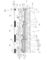
図4は、有機EL表示装置の全体構成を示す断面図、図5は、各サブ画素における画素電極の膜厚を示す模式図である。また、図6は、絶縁膜の構成を1画素領域に着目して示す平面図である。
本実施形態の有機EL表示装置100は、トップエミッション構造であって、図4に示すように、基板10A上の表示領域4(図1)内におけるサブ画素3R,3B,3Gごとに、有機EL素子7とこの有機EL素子7を発光駆動させる駆動回路8とが設けられたアクティブマトリクス基板10と、アクティブマトリクス基板10上に電気光学層30を介して対向配置されたカラーフィルター基板20とを備えている。
FIG. 4 is a cross-sectional view showing the overall configuration of the organic EL display device, and FIG. 5 is a schematic diagram showing the film thickness of the pixel electrode in each sub-pixel. FIG. 6 is a plan view showing the structure of the insulating film with a focus on one pixel region.
The organic
以下、各構成要素について具体的に述べる。
図4に示すように、駆動回路8は、基板10A上に形成されたデバイス層12の内部に形成され、薄膜トランジスタ(不図示)、駆動トランジスタ123、保持容量113、画素電極16により構成される。
薄膜トランジスタ(不図示)および駆動トランジスタ123は、基板10A上に形成された半導体層41aのドレイン領域に接続されたドレイン電極41dと、半導体層41aのソース領域と接続されたソース電極41cと、半導体層41aを覆うゲート絶縁膜41b上に形成されたゲート電極41eとで構成されている。ドレイン電極41dおよびソース電極41cは層間絶縁膜43上に形成されている。そして、ドレイン電極41dは、電源供給線103に接続され、ソース電極41cは、ソース電極41cおよびドレイン電極41dを覆うように形成されたカバー層44および平坦化膜45,46を貫通して形成された各コンタクトホールHを介して、対応する各画素電極16R,16G,16Bと接続されている。
Each component will be specifically described below.
As shown in FIG. 4, the
The thin film transistor (not shown) and the driving
本実施形態の有機EL表示装置100はトップエミッション構造を有していることから、有機EL素子7の発光光が対向電極18側から射出するように、画素電極16R,16G,16Bと基板10Aとの間には各サブ画素3R,3G,3Bに対応する反射層14が複数設けられている。
Since the organic
反射層14は、デバイス層12の表面上にサブ画素3R,3B,3Gごとにパターン形成されたものであり、光反射率の高い材料より形成されている。反射層14の形成材料として、例えば、アルミニウム、銀、あるいは銀の合金などが挙げられる。反射層14は、有機EL素子7の発光光のうち、画素電極16R,16G,16Bを透過して基板10A側に射出される光を反射して対向電極18側へと射出させる。なお、反射層14は、デバイス層12の表面上の領域(コンタクトホールHの形成領域を除く領域)全体にベタ状に形成されていてもよい。
The
デバイス層12(平坦化層46)の表面上には、サブ画素3R,3B,3Gごとに膜厚の異なる画素電極16R,16G,16Bが形成されている。この画素電極16R,16G,16Bは、その全てが平面視において反射層14と重なる領域に形成されており、複数の透明電極膜による積層構造あるいは、単一の透明電極膜による単層構造とされている。具体的には、画素3Rの画素電極16Rは3層の透明電極膜(電極層)16a,16b,16cからなり、画素3Gの画素電極16Gは2層の透明電極膜16b,16cからなり、画素3Bの画素電極16Bは1層の透明電極膜16cからなっている。
On the surface of the device layer 12 (flattening layer 46),
各画素電極16R,16G,16Bを形成する際には、まず、画素3Rに対応する領域に膜厚40nmの第1透明電極膜16aを形成する。その後、第1透明電極膜16aの略全体を覆うようにして第2透明電極膜16bを形成し、同時に、画素3Gに対応する領域にも第2透明電極膜16bを形成する。この第2透明電極膜16bの膜厚は40nmである。
When forming each
次に、画素3Rおよび画素3G内に第2透明電極膜16bの略全体を覆うようにして膜厚20nmの第3透明電極膜16cを形成し、同時に、画素3Bに対応する領域にも第3透明電極膜16cを形成する。この結果、図5に示すように、画素3Rの画素電極16Rの膜厚t1は100nm、画素3Gの画素電極16Gの膜厚t2は60nm、画素3Bの画素電極16Bの膜厚t3は20nmとなる。このようにして、サブ画素3R,3B,3Gごとに総膜厚の異なる画素電極16R,16G,16Bを設ける。なお、平面視矩形状を呈する画素電極16R,16G,16Bの大きさ(表面積)は互いに等しい。このような画素電極16R,16G,16Bの周縁部は絶縁膜22によって覆われている。
Next, a third
絶縁膜22は、デバイス層12の表面12a(露出した部分)から各画素電極16R,16G,16Bの表面161上に一部乗り上げるようにして周縁部162を覆い、所定の膜厚で形成されている。本実施形態における絶縁膜22の膜厚は20nmである。ここで、隣り合う画素電極16R,16G,16Bどうしの総膜厚は異なるものの、隣り合うサブ画素3R,3B,3G間に形成される絶縁膜22の厚さは一定であり、同一工程においてパターン形成される。
デバイス層12の表面12aと各画素電極16R,16G,16Bの表面161との間に形成される段差部Qはこの絶縁膜22によって覆われている。
The insulating
The step portion Q formed between the
本実施形態の絶縁膜22は、各画素電極16R,16G,16Bの表面中央側を部分的に露出させるとともに、各色のサブ画素3R,3B,3Gごとに開口面積を異ならせた開口22R,22G,22Bを有している。開口面積を各色のサブ画素3R,3B,3Gごとに異ならせることにより、これよりも上層に積層される有機EL発光層19の発光領域を制御することができる。
具体的に、各色に対応する開口22R,22G,22Bはどれも平面視における画素電極16R,16G,16Bの表面積よりも小さい開口面積を有し、反射層14と対向電極18の間の反射によって共振する光の波長に応じた開口面積に調整されている。
The insulating
Specifically, each of the
図6に示すように、絶縁膜22に形成された開口22R,22G,22Bの長手方向の長さL3は各サブ画素3R,3G,3Bで等しく、例えば11μmである。短手方向の幅W1,W2,W3は色毎に異なっており、W1=2.5μm、W2=3.0μm、W3=3.5μmである。よって、各色に対応する開口面積の関係は、サブ画素3Rの開口面積<サブ画素3Gの開口面積<サブ画素3Bの開口面積となり、共振する光の波長が短い色の画素ほど開口面積が大きい。絶縁膜22に形成された各開口22R,22G,22Bの開口面積に応じて上記した各サブ画素3R,3B,3Gの発光領域が設定されることになる。
図4に戻り、絶縁膜22とその各開口22R,22G,22Bから露出する画素電極16R,16G,16Bの表面161を覆うようにして有機EL発光層19が形成されている。
As shown in FIG. 6, the length L3 in the longitudinal direction of the
Returning to FIG. 4, the organic EL
有機EL発光層19は、画素電極16R,16G,16B側から、例えば、正孔注入層(HIL)、正孔輸送層(HTL)、発光層(EML)、電子輸送層などの、有機層からなる各機能層(有機EL発光層19以外は不図示)が順に積層されたものであり、積層された複数の機能層の総厚は、R,G,Bの各サブ画素3R,3B,3Gにおいて略同じ厚さで形成されている。
The organic EL
また、各機能層は、例えば、アミン系有機材料などといった有機材料によって形成されている。有機EL発光層19は、青色発光機能層と黄色発光機能層が積層され、発光領域から白色光を射出するように構成されている。なお、有機EL素子7を構成する各機能層は、これに限定されず、正孔注入層と正孔輸送層とが同一層とされた構成や、有機EL発光層19が全ての機能層を兼ねた構成など、他の構成であっても良い。
Each functional layer is formed of an organic material such as an amine organic material. The organic EL
対向電極18は、半透過反射性を有する材料を用いて、有機EL発光層19の表面全体にベタ状に形成されている。上記した画素電極16は導電性を有するとともに光透過性を有する材料で形成されている。一方、光路中に存在する対向電極18は、例えば光が透過する程度に薄く形成された金属材料や、光透過性と光反射性を両方備えた材料で形成されている。これにより、反射層14において反射された光は画素電極16を透過して対向電極18へと入射し、その一部が画素電極16側へ反射され、再び反射層14で反射されることになる。この結果、反射層14と対向電極18との間の光路長に応じた波長を有する光が、反射層14と対向電極18との間で共振し、共振した光が対向電極18側から射出されることになる。
The
アクティブマトリクス基板10上に電気光学層30を介して対向配置されるカラーフィルター基板20は、ガラス基板などの透明基板20A上に遮光膜21によって区画されたRフィルター2R、Gフィルター2G、Bフィルター2Bが各色に対応するサブ画素3R,3B,3Gの配列に合わせて形成されたものであって、各フィルター2R,2G,2Bは各サブ画素3R,3G,3Bの発光領域と重なるように配置されている。各フィルター2R,2G,2Bの形状は、各開口22R,22G,22Bの平面形状に沿った矩形形状とされている。また、これら各フィルター2R,2G,2Bの表面積は、それぞれ対応する絶縁膜22の各開口22R,22G,22Bの開口面積に略等しい。
The
そして、サブ画素3R,3G,3Bの各発光領域から射出された白色光は、Rフィルター2R、Gフィルター2G、Bフィルター2Bによって、それぞれR光、G光、B光に変換される。よって、各発光領域の明るさに応じた色の光が各フィルター2R,2G,2Bから射出されることによって、それぞれ各サブ画素3R,3G,3Bを形成してカラー画像が表示される。
The white light emitted from the light emitting regions of the sub-pixels 3R, 3G, and 3B is converted into R light, G light, and B light by the
本実施形態の有機EL表示装置100は、白色の有機EL発光層19が形成される基板10A側には光の3原色であるRGB内にそれぞれ膜厚の異なる画素電極16R,16G,16Bが形成されている。このため、画素電極16R,16G,16Bの下方に位置する反射層14と、画素電極16R,16G,16Bの上方に位置する対向電極18との間にそれぞれ異なる光共振構造が形成され、発光領域において各RGBに対応した3種類の異なる発光スペクトルが得られるようになっている。
In the organic
膜厚の異なる画素電極16R,16G,16Bの各表面161と基板10Aの表面との間には大きさの異なる段差部Qが生じてしまう。本実施形態では、透明電極層の積層数を異ならせることで画素電極16R,16G,16Bの総膜厚を変化させている。このため、積層構造とされた画素電極16R,16Gの周縁部分は薄く形成され、この部分的に薄くなった画素電極16R,16G,16Bの周縁部分、すなわち段差部Qと対向電極18との間では光路長さが変化してしまい、所望の発光スペクトルとは異なる発光スペクトルとなって不要な光が射出されてしまう。
Stepped portions Q having different sizes are generated between the
そこで、本実施形態では、このような画素電極16R,16G,16Bの段差部Qの全体を覆うようにして、デバイス層12の表面から画素電極16R,16G,16Bの表面161上(周縁部162)にかけて絶縁膜22を形成することで、画素電極16R,16G,16Bの段差部Q(周縁部162も含む)と有機EL発光層19とを部分的に絶縁し、段差部Q上の有機EL発光層19に電流が流れないようにしている。これにより、積層構造を有する画素電極16R,16G,16Bの側面に段差部Qが形成されたとしても、段差部Q上の有機EL発光層19から所望しない発光スペクトルの光が射出されてしまうのを防止することができる。よって、絶縁膜22の開口22R,22G,22Bの周辺部分で色むらが生じることが防止され、各サブ画素3R,3G,3Bからは所望とする発光スペクトルの光が得られることになる。
Therefore, in the present embodiment, the entire stepped portion Q of the
また、本実施形態では、画素電極16R,16G,16Bと駆動回路8との導通領域を覆うようにして絶縁膜22が形成されている。画素電極16R,16G,16Bは、層間絶縁膜に形成されたコンタクトホールHを介して、駆動回路8の駆動トランジスタ123のドレイン電極41dに接続されている。このコンタクトホールHが形成される箇所には反射層14を形成することができないため、共振構造とすることができない。このため、コンタクトホールH上の有機EL発光層19が発光しないようにこのような導通領域を絶縁膜22で覆った構成となっている。これにより、各サブ画素3R,3G,3Bから純粋な色のR光、G光、B光が得られるようになる。
In the present embodiment, the insulating
また、本実施形態では、絶縁膜22に形成された開口22R,22G,22Bの開口面積をサブ画素3R,3B,3Gごとに異ならせてある。つまり、絶縁膜22の各開口22R,22G,22Bの大きさによってRGBに対応する各有機EL素子7の発光面積を制御している。
In the present embodiment, the opening areas of the
各サブ画素3R,3G,3Bには同じ構成を有する駆動回路8が設けられている。このため、各駆動回路8に同じ電流を流したとしても波長の異なるサブ画素3R,3G,3B間では光具合が違ってくる。そこで、絶縁膜22の開口面積の大きさを異ならせてサブ画素3R,3G,3Bの発光面積を制御することによって、各サブ画素3R,3G,3Bにおける発光状態を整えることが可能となる。
Each
ここで、RGBの各波長の関係は、青色の波長<緑色の波長<赤色の波長となっている。このため、各色のサブ画素3R,3G,3Bに対応する開口22R,22G,22Bの開口面積の関係としては、波長が短い色ほど開口面積が大きくなるように設定する。つまり、開口22Rの開口面積<開口22Gの開口面積<開口22Bの開口面積とすることによって、各サブ画素3R,3G,3Bにおける光の強さを均一にすることが可能となる。
Here, the relationship between the wavelengths of RGB is blue wavelength <green wavelength <red wavelength. For this reason, the relationship between the aperture areas of the
これにより、各サブ画素3R,3G,3Bからは発光光量が略等しいR光,G光,B光のいわゆる3原色の光が射出され、サブ画素3R,3G,3B間におけるカラーバランスを整えることができる。したがって、白色有機材料の特性に合わせた発光領域の制御をサブ画素3R,3G,3Bごとに行うことによって、最適な色合成を実現することができる。 As a result, light of the three primary colors of R light, G light, and B light having substantially equal amounts of emitted light is emitted from the sub-pixels 3R, 3G, and 3B, and the color balance between the sub-pixels 3R, 3G, and 3B is adjusted. Can do. Therefore, optimal color composition can be realized by controlling the light emitting region in accordance with the characteristics of the white organic material for each of the sub-pixels 3R, 3G, and 3B.
また、本実施形態の構成によれば、画素ピッチをサブ画素3R,3G,3Bごとに制御する必要がないことから狭ピッチな画素配列を実現でき、マイクロディスプレイなどの微小な表示画面にも対応可能となる。 In addition, according to the configuration of the present embodiment, since it is not necessary to control the pixel pitch for each of the sub-pixels 3R, 3G, and 3B, it is possible to realize a pixel arrangement with a narrow pitch, and it is also compatible with a micro display screen such as a micro display. It becomes possible.
[第2実施形態]
次に、本発明の第2実施形態の有機EL表示装置について説明する。
図7は、第2実施形態の有機EL表示装置の概略構成を示す断面図である。
以下に示す本実施形態の有機EL表示装置の基本構成は、上記第1実施形態と略同様であるが、絶縁膜の構成において異なる。よって、以下の説明では、絶縁膜の構成について詳しく説明し、共通な箇所の説明は省略する。また、説明に用いる各図面において、図1〜図6と共通の構成要素には同一の符号を付すものとする。
[Second Embodiment]
Next, an organic EL display device according to a second embodiment of the present invention will be described.
FIG. 7 is a cross-sectional view illustrating a schematic configuration of the organic EL display device according to the second embodiment.
The basic configuration of the organic EL display device of the present embodiment described below is substantially the same as that of the first embodiment, but is different in the configuration of the insulating film. Therefore, in the following description, the structure of the insulating film will be described in detail, and description of common portions will be omitted. Moreover, in each drawing used for description, the same code | symbol shall be attached | subjected to the same component as FIGS.
上記実施形態における有機EL表示装置200では、絶縁膜22が、画素電極16R,16G,16Bの段差部Qを覆うようにしてサブ画素3R,3G,3B間で一定の膜厚で形成されている。このため、絶縁膜52は、画素電極16R,16G,16Bの段差部Qの形状を反映させるようにして形成されることから、その表面に微細な凹凸が形成されて、有機EL材料の付きまわりが低下するおそれがある。有機EL発光層19の膜厚が不均一になると対向電極18の膜厚に影響が出てしまう。
In the organic
そこで、本実施形態の有機EL表示装置200は、サブ画素3R,3G,3B間の絶縁膜52の膜厚を部分的に厚く形成することにより、開口52R,52G,52Bを除くサブ画素3R,3G,3B間に生じた段差部分、つまり、画素電極16R,16G,16Bの各段差部Q上の表面形状を平坦化する構成とした。
絶縁膜52の表面52aの高さ位置はサブ画素3R,3G,3B間で一致する。すなわち、サブ画素3Rとサブ画素3Gとの間に存在する絶縁膜52の膜厚と、サブ画素3Gとサブ画素3Bとの間に存在する絶縁膜52の膜厚は略等しい。
Therefore, in the organic
The height position of the
ここで、各開口52R,52G,52Bはカラーフィルター基板20側に向かってテーパー状に広がるように形成されており、これによって画素電極16R,16G,16Bの表面161と絶縁膜52の表面52aの間に形成される段差が緩和され、有機EL材料の付きまわりを良くすることができる。これにより、有機EL発光層19が局所的に薄く形成されるのを防止できる。
Here, the
有機EL材料の付きまわりが悪い場合、その部位では有機EL発光層19が局所的に薄膜化し、平坦部位と比較して薄膜化した部分に大きな電流が流れてしまう。この場合、所望とする発光領域の周辺が発光してしまうことになる。
このため、本実施形態のように、画素電極16R,16G,16Bの周縁部分に形成される段差部Qの形状が反映されないように、隣り合う画素電極16R,16G,16B同士の間において絶縁膜52の膜厚を部分的に厚膜化することにより、その表面52a上に形成される有機EL発光層19の材料の付きまわりを良くすることができる。これにより、有機EL発光層19が部分的に薄膜化してこの部分に電流が流れてしまうことが防止されるので、開口周辺における意図しない発光をなくすことができる。これにより、各サブ画素3R,3G,3Bから純粋な色のR光、G光、B光が得られるようになる。
When the organic EL material is poorly attached, the organic EL
Therefore, as in the present embodiment, the insulating film is formed between the
また、絶縁膜52の各開口52R,52G,52Bがカラーフィルター基板20側に向けて拡がるようにテーパー状に形成されていることから、画素電極16R,16G,16Bの周縁部162を覆う絶縁膜52の開口周縁部分、つまり、絶縁膜52の表面52aと画素電極16R,16G,16Bの表面161との間に段差が形成されることが防止される。これにより、画素電極16R,16G,16B上における有機EL発光層19が局所的に薄膜化してしまうのを防ぐことができるので、開口周辺部分において意図しない発光が生じるのをより防止することができる。
In addition, since the
また、このように画素電極16R,16G,16Bの周縁段差を緩和するように絶縁膜52を厚く形成することで、有機EL発光層19の局所的な薄膜化を防止できるとともにその上に積層される対向電極18の膜厚を均一にすることが可能となる。
互いに隣り合う表示単位画素3どうしの間(図7の左端の部分)の距離L2は、各表示単位画素3内の各サブ画素3R,3B,3G同士の距離L1よりも大きく(L1<L2)なっていることから、段差の影響が小さくなる。言い換えれば、各サブ画素3R,3B,3G同士の間では段差の影響が大きいことになる。そのため、各サブ画素3R,3B,3G同士の間の絶縁膜52の厚さを、表示単位画素3どうしの間の絶縁膜52(図7の左端または右端)よりも厚くすることが好ましい。
このように、絶縁膜52の膜厚を部分的異ならせることで段差による影響を抑えることが可能である。
In addition, by forming the insulating
The distance L2 between the
In this way, by partially varying the thickness of the insulating
以上、添付図面を参照しながら本発明に係る好適な実施形態について説明したが、本発明は係る例に限定されないことは言うまでもない。当業者であれば、特許請求の範囲に記載された技術的思想の範疇内において、各種の変更例または修正例に想到し得ることは明らかであり、それらについても当然に本発明の技術的範囲に属するものと了解される。 As described above, the preferred embodiments according to the present invention have been described with reference to the accompanying drawings, but the present invention is not limited to the examples. It is obvious for those skilled in the art that various changes or modifications can be conceived within the scope of the technical idea described in the claims. It is understood that it belongs to.
例えば、第2実施形態において、絶縁膜52の各開口52R,52G,52Bがテーパー形状をなすものに限らず、絶縁膜52の表面52aと画素電極16R,16G,16Bの表面161との間の段差が緩和され、有機EL発光層19の局所的な薄膜化を防止できればよい。
For example, in the second embodiment, each
3B,3G,3R…サブ画素、Q…段差部、10A…基板、12a,52a,161…表面、14…反射層、16…画素電極(第1電極)、16a…透明電極膜(電極層)、18…対向電極(第2電極)、19…有機EL発光層(発光層)、22,52…絶縁膜、22B,22G,22R,52R、52G,52B…開口、t1,t2,t3…膜厚、100,200…有機EL表示装置、162…周縁部 3B, 3G, 3R ... sub-pixel, Q ... stepped portion, 10A ... substrate, 12a, 52a, 161 ... surface, 14 ... reflective layer, 16 ... pixel electrode (first electrode), 16a ... transparent electrode film (electrode layer) , 18 ... counter electrode (second electrode), 19 ... organic EL light emitting layer (light emitting layer), 22, 52 ... insulating film, 22B, 22G, 22R, 52R, 52G, 52B ... opening, t1, t2, t3 ... film Thickness, 100, 200 ... organic EL display device, 162 ... peripheral edge
Claims (6)
前記第1サブ画素及び第2サブ画素の各々は、基板上に順に形成された、光を反射する反射層と、光透過性を有する第1電極と、前記第1電極を覆う有機層と、半透過反射性を有する第2電極と、を含み、
前記反射層が前記画素ごとにパターン形成されており、
前記反射層と前記第2電極の間の反射によって共振する光の波長が前記第1サブ画素と前記第2サブ画素とで異なっており、
前記基板上には、前記第1電極の周縁部分を覆うようにして絶縁膜が設けられ、
前記絶縁膜は、前記第1電極の表面を部分的に露出させるとともに前記第1サブ画素の第1開口面積が前記第2サブ画素の第2開口面積と異ならせた開口を有し、
前記第1サブ画素及び第2サブ画素の間の距離L1と前記画素同士の間の距離L2とがL1<L2の関係にある
ことを特徴とする有機EL表示装置。 An organic EL display device comprising a plurality of pixels, each of the plurality of pixels having at least a first sub-pixel and a second sub-pixel that emit light of different wavelengths,
Each of the first sub-pixel and the second sub-pixel includes a reflective layer that reflects light, a first electrode that transmits light, an organic layer that covers the first electrode, A second electrode having transflective properties,
The reflective layer is patterned for each pixel;
The wavelength of light resonated by reflection between the reflective layer and the second electrode is different between the first sub-pixel and the second sub-pixel,
An insulating film is provided on the substrate so as to cover a peripheral portion of the first electrode,
The insulating film has an opening in which a surface of the first electrode is partially exposed and a first opening area of the first sub-pixel is different from a second opening area of the second sub-pixel;
The organic EL display device , wherein a distance L1 between the first subpixel and the second subpixel and a distance L2 between the pixels are in a relationship of L1 <L2 .
前記第1開口面積は前記第2開口面積より大きい
ことを特徴とする請求項1に記載の有機EL表示装置。 The wavelength of light that the first sub-pixel resonates is shorter than the wavelength of light that the second sub-pixel resonates.
The organic EL display device according to claim 1, wherein the first opening area is larger than the second opening area.
前記第1サブ画素における開口の短手方向の長さは、前記第1サブ画素における開口の短手方向の長さより長いThe length in the short direction of the opening in the first sub-pixel is longer than the length in the short direction of the opening in the first sub-pixel.
ことを特徴とする請求項2に記載の有機EL表示装置。The organic EL display device according to claim 2.
前記第1電極の前記表面と前記基板の表面との間に形成される段差部分が前記絶縁膜によって覆われている
ことを特徴とする請求項1から3のいずれか一項に記載の有機EL表示装置。 The first electrode is composed of a single electrode layer or a plurality of stacked electrode layers,
The organic EL according to any one of claims 1 to 3, the step portion to be formed and being covered by the insulating film between the surface and the substrate surface of the first electrode Display device.
ことを特徴とする請求項1から4のいずれか一項に記載の有機EL表示装置。 The insulating film formed between the first sub-pixel and the second sub-pixel is formed thicker than the insulating film formed in a region between the pixels. The organic EL display device according to any one of claims 1 to 4 .
ことを特徴とする請求項1から5のいずれか一項に記載の有機EL表示装置。 6. The organic EL display device according to claim 1, wherein a size of the first electrode in plan view is equal between the first sub-pixel and the second sub-pixel. 7.
Priority Applications (1)
| Application Number | Priority Date | Filing Date | Title |
|---|---|---|---|
| JP2011214084A JP5831100B2 (en) | 2011-09-29 | 2011-09-29 | Organic EL display device |
Applications Claiming Priority (1)
| Application Number | Priority Date | Filing Date | Title |
|---|---|---|---|
| JP2011214084A JP5831100B2 (en) | 2011-09-29 | 2011-09-29 | Organic EL display device |
Publications (3)
| Publication Number | Publication Date |
|---|---|
| JP2013073884A JP2013073884A (en) | 2013-04-22 |
| JP2013073884A5 JP2013073884A5 (en) | 2014-10-30 |
| JP5831100B2 true JP5831100B2 (en) | 2015-12-09 |
Family
ID=48478209
Family Applications (1)
| Application Number | Title | Priority Date | Filing Date |
|---|---|---|---|
| JP2011214084A Active JP5831100B2 (en) | 2011-09-29 | 2011-09-29 | Organic EL display device |
Country Status (1)
| Country | Link |
|---|---|
| JP (1) | JP5831100B2 (en) |
Cited By (2)
| Publication number | Priority date | Publication date | Assignee | Title |
|---|---|---|---|---|
| KR20190070192A (en) * | 2017-12-12 | 2019-06-20 | 엘지디스플레이 주식회사 | Electroluminescent Display Device |
| KR20190072824A (en) * | 2017-12-18 | 2019-06-26 | 엘지디스플레이 주식회사 | Electroluminescent Display Device |
Families Citing this family (7)
| Publication number | Priority date | Publication date | Assignee | Title |
|---|---|---|---|---|
| JP6221418B2 (en) * | 2013-07-01 | 2017-11-01 | セイコーエプソン株式会社 | LIGHT EMITTING DEVICE AND ELECTRONIC DEVICE |
| JP6318676B2 (en) * | 2014-02-14 | 2018-05-09 | セイコーエプソン株式会社 | Organic light emitting device manufacturing method, organic light emitting device, and electronic apparatus |
| JP6504206B2 (en) | 2017-06-30 | 2019-04-24 | セイコーエプソン株式会社 | Electro-optical device and electronic device |
| US20210036254A1 (en) * | 2018-03-22 | 2021-02-04 | Sharp Kabushiki Kaisha | Light emitting element and display device |
| KR20200089379A (en) | 2019-01-16 | 2020-07-27 | 삼성디스플레이 주식회사 | Organic light emitting display apparatus |
| JP7458847B2 (en) | 2020-03-24 | 2024-04-01 | キヤノン株式会社 | Display and electronic devices |
| CN114167639B (en) * | 2020-09-11 | 2024-02-27 | 成都辰显光电有限公司 | Display panel, display device and control method of display panel |
Family Cites Families (5)
| Publication number | Priority date | Publication date | Assignee | Title |
|---|---|---|---|---|
| JP3670923B2 (en) * | 1999-02-26 | 2005-07-13 | 三洋電機株式会社 | Color organic EL display device |
| US6747618B2 (en) * | 2002-08-20 | 2004-06-08 | Eastman Kodak Company | Color organic light emitting diode display with improved lifetime |
| JP2005197009A (en) * | 2003-12-26 | 2005-07-21 | Sanyo Electric Co Ltd | Manufacturing method and manufacturing device of display device |
| JP5515237B2 (en) * | 2008-05-14 | 2014-06-11 | セイコーエプソン株式会社 | LIGHT EMITTING DEVICE AND ELECTRONIC DEVICE |
| JP5195593B2 (en) * | 2009-04-01 | 2013-05-08 | セイコーエプソン株式会社 | ORGANIC EL DEVICE, METHOD FOR MANUFACTURING ORGANIC EL DEVICE, AND ELECTRONIC DEVICE |
-
2011
- 2011-09-29 JP JP2011214084A patent/JP5831100B2/en active Active
Cited By (4)
| Publication number | Priority date | Publication date | Assignee | Title |
|---|---|---|---|---|
| KR20190070192A (en) * | 2017-12-12 | 2019-06-20 | 엘지디스플레이 주식회사 | Electroluminescent Display Device |
| KR102455567B1 (en) | 2017-12-12 | 2022-10-14 | 엘지디스플레이 주식회사 | Electroluminescent Display Device |
| KR20190072824A (en) * | 2017-12-18 | 2019-06-26 | 엘지디스플레이 주식회사 | Electroluminescent Display Device |
| KR102513910B1 (en) | 2017-12-18 | 2023-03-23 | 엘지디스플레이 주식회사 | Electroluminescent Display Device |
Also Published As
| Publication number | Publication date |
|---|---|
| JP2013073884A (en) | 2013-04-22 |
Similar Documents
| Publication | Publication Date | Title |
|---|---|---|
| JP5831100B2 (en) | Organic EL display device | |
| CN107195584B (en) | Preparation method of display panel, display panel and display device | |
| KR101448003B1 (en) | Organic light emitting diode display and method for manufacturing the same | |
| JP6542867B2 (en) | Display device | |
| JP4741492B2 (en) | OLED device with microcavity gamut subpixel | |
| JP4895490B2 (en) | Organic EL panel | |
| KR102033348B1 (en) | Organic Light Emitting Diode Display Device and Method for Manufacturing The Same | |
| KR101404546B1 (en) | Organic light emitting diode display and method for manufacturing the same | |
| US7531958B2 (en) | Organic EL element and organic EL panel having microresonator and color filter | |
| KR101317577B1 (en) | Organic electroluminescent display device | |
| US20100060148A1 (en) | Organic light emitting diode display | |
| JP2010050014A (en) | Light-emitting device and electronic equipment | |
| JP6111643B2 (en) | ORGANIC ELECTROLUMINESCENCE DEVICE AND ELECTRONIC DEVICE | |
| US8659512B2 (en) | Organic light emitting diode display and method for manufacturing the same | |
| KR101566271B1 (en) | Organic light emitting diode display and method for manufacturing the same | |
| EP2744010A1 (en) | Array Substrate and Method for Manufacturing the same, Display Device | |
| KR20100026738A (en) | Organic light emitting diode display and method for manufacturing the same | |
| TWI303136B (en) | Method for manufacturing electro-optic element | |
| JP4858054B2 (en) | LIGHT EMITTING DEVICE AND ELECTRONIC DEVICE | |
| JP2010010020A (en) | Light emitting device, and method for thereof | |
| JP2013089444A (en) | Organic light-emitting device, manufacturing method therefor and electronic apparatus | |
| WO2013099744A1 (en) | Display device | |
| JP6492403B2 (en) | Organic EL device, method for manufacturing organic EL device, electronic device | |
| JP5786675B2 (en) | Organic light emitting device | |
| CN109560115B (en) | Preparation method of display panel, display panel and display device |
Legal Events
| Date | Code | Title | Description |
|---|---|---|---|
| A521 | Request for written amendment filed |
Free format text: JAPANESE INTERMEDIATE CODE: A523 Effective date: 20140912 |
|
| A621 | Written request for application examination |
Free format text: JAPANESE INTERMEDIATE CODE: A621 Effective date: 20140912 |
|
| RD04 | Notification of resignation of power of attorney |
Free format text: JAPANESE INTERMEDIATE CODE: A7424 Effective date: 20150107 |
|
| A977 | Report on retrieval |
Free format text: JAPANESE INTERMEDIATE CODE: A971007 Effective date: 20150608 |
|
| A131 | Notification of reasons for refusal |
Free format text: JAPANESE INTERMEDIATE CODE: A131 Effective date: 20150616 |
|
| A521 | Request for written amendment filed |
Free format text: JAPANESE INTERMEDIATE CODE: A523 Effective date: 20150810 |
|
| TRDD | Decision of grant or rejection written | ||
| A01 | Written decision to grant a patent or to grant a registration (utility model) |
Free format text: JAPANESE INTERMEDIATE CODE: A01 Effective date: 20150929 |
|
| A61 | First payment of annual fees (during grant procedure) |
Free format text: JAPANESE INTERMEDIATE CODE: A61 Effective date: 20151012 |
|
| R150 | Certificate of patent or registration of utility model |
Ref document number: 5831100 Country of ref document: JP Free format text: JAPANESE INTERMEDIATE CODE: R150 |
|
| S531 | Written request for registration of change of domicile |
Free format text: JAPANESE INTERMEDIATE CODE: R313531 |
|
| R350 | Written notification of registration of transfer |
Free format text: JAPANESE INTERMEDIATE CODE: R350 |