JP4741492B2 - OLED device with microcavity gamut subpixel - Google Patents
OLED device with microcavity gamut subpixel Download PDFInfo
- Publication number
- JP4741492B2 JP4741492B2 JP2006523907A JP2006523907A JP4741492B2 JP 4741492 B2 JP4741492 B2 JP 4741492B2 JP 2006523907 A JP2006523907 A JP 2006523907A JP 2006523907 A JP2006523907 A JP 2006523907A JP 4741492 B2 JP4741492 B2 JP 4741492B2
- Authority
- JP
- Japan
- Prior art keywords
- gamut
- sub
- pixels
- pixel
- color
- Prior art date
- Legal status (The legal status is an assumption and is not a legal conclusion. Google has not performed a legal analysis and makes no representation as to the accuracy of the status listed.)
- Active
Links
- 239000010410 layer Substances 0.000 claims description 69
- 125000006850 spacer group Chemical group 0.000 claims description 34
- 239000000463 material Substances 0.000 claims description 17
- 239000012044 organic layer Substances 0.000 claims description 9
- 239000011159 matrix material Substances 0.000 description 23
- XLOMVQKBTHCTTD-UHFFFAOYSA-N Zinc monoxide Chemical compound [Zn]=O XLOMVQKBTHCTTD-UHFFFAOYSA-N 0.000 description 16
- 239000000758 substrate Substances 0.000 description 13
- 239000003086 colorant Substances 0.000 description 11
- 229910003437 indium oxide Inorganic materials 0.000 description 8
- PJXISJQVUVHSOJ-UHFFFAOYSA-N indium(iii) oxide Chemical compound [O-2].[O-2].[O-2].[In+3].[In+3] PJXISJQVUVHSOJ-UHFFFAOYSA-N 0.000 description 8
- 229910000476 molybdenum oxide Inorganic materials 0.000 description 8
- 239000011787 zinc oxide Substances 0.000 description 8
- 229910045601 alloy Inorganic materials 0.000 description 7
- 239000000956 alloy Substances 0.000 description 7
- 239000004020 conductor Substances 0.000 description 7
- 238000000059 patterning Methods 0.000 description 7
- 229910052737 gold Inorganic materials 0.000 description 6
- 229910052709 silver Inorganic materials 0.000 description 6
- 238000002347 injection Methods 0.000 description 5
- 239000007924 injection Substances 0.000 description 5
- 239000004065 semiconductor Substances 0.000 description 5
- 229910018316 SbOx Inorganic materials 0.000 description 4
- 229910006854 SnOx Inorganic materials 0.000 description 4
- 229910052782 aluminium Inorganic materials 0.000 description 4
- 238000010586 diagram Methods 0.000 description 4
- AMGQUBHHOARCQH-UHFFFAOYSA-N indium;oxotin Chemical compound [In].[Sn]=O AMGQUBHHOARCQH-UHFFFAOYSA-N 0.000 description 4
- 229910044991 metal oxide Inorganic materials 0.000 description 4
- 150000004706 metal oxides Chemical class 0.000 description 4
- PQQKPALAQIIWST-UHFFFAOYSA-N oxomolybdenum Chemical compound [Mo]=O PQQKPALAQIIWST-UHFFFAOYSA-N 0.000 description 4
- KYKLWYKWCAYAJY-UHFFFAOYSA-N oxotin;zinc Chemical compound [Zn].[Sn]=O KYKLWYKWCAYAJY-UHFFFAOYSA-N 0.000 description 4
- 229910052714 tellurium Inorganic materials 0.000 description 4
- PORWMNRCUJJQNO-UHFFFAOYSA-N tellurium atom Chemical compound [Te] PORWMNRCUJJQNO-UHFFFAOYSA-N 0.000 description 4
- XOLBLPGZBRYERU-UHFFFAOYSA-N tin dioxide Chemical compound O=[Sn]=O XOLBLPGZBRYERU-UHFFFAOYSA-N 0.000 description 4
- 229910001887 tin oxide Inorganic materials 0.000 description 4
- 229910000410 antimony oxide Inorganic materials 0.000 description 3
- 230000008021 deposition Effects 0.000 description 3
- 230000005525 hole transport Effects 0.000 description 3
- VTRUBDSFZJNXHI-UHFFFAOYSA-N oxoantimony Chemical compound [Sb]=O VTRUBDSFZJNXHI-UHFFFAOYSA-N 0.000 description 3
- ORFSSYGWXNGVFB-UHFFFAOYSA-N sodium 4-amino-6-[[4-[4-[(8-amino-1-hydroxy-5,7-disulfonaphthalen-2-yl)diazenyl]-3-methoxyphenyl]-2-methoxyphenyl]diazenyl]-5-hydroxynaphthalene-1,3-disulfonic acid Chemical compound COC1=C(C=CC(=C1)C2=CC(=C(C=C2)N=NC3=C(C4=C(C=C3)C(=CC(=C4N)S(=O)(=O)O)S(=O)(=O)O)O)OC)N=NC5=C(C6=C(C=C5)C(=CC(=C6N)S(=O)(=O)O)S(=O)(=O)O)O.[Na+] ORFSSYGWXNGVFB-UHFFFAOYSA-N 0.000 description 3
- 239000003990 capacitor Substances 0.000 description 2
- 238000009413 insulation Methods 0.000 description 2
- 238000000034 method Methods 0.000 description 2
- 230000003287 optical effect Effects 0.000 description 2
- 239000010409 thin film Substances 0.000 description 2
- 229910052787 antimony Inorganic materials 0.000 description 1
- WATWJIUSRGPENY-UHFFFAOYSA-N antimony atom Chemical compound [Sb] WATWJIUSRGPENY-UHFFFAOYSA-N 0.000 description 1
- 150000001875 compounds Chemical class 0.000 description 1
- 230000005684 electric field Effects 0.000 description 1
- 239000010931 gold Substances 0.000 description 1
- 238000004020 luminiscence type Methods 0.000 description 1
- 238000004519 manufacturing process Methods 0.000 description 1
- 229910052751 metal Inorganic materials 0.000 description 1
- 239000002184 metal Substances 0.000 description 1
- 150000002739 metals Chemical class 0.000 description 1
- 238000012986 modification Methods 0.000 description 1
- 230000004048 modification Effects 0.000 description 1
- 238000005215 recombination Methods 0.000 description 1
- 230000006798 recombination Effects 0.000 description 1
- -1 rubrene compound Chemical class 0.000 description 1
- 239000010944 silver (metal) Substances 0.000 description 1
- 230000003595 spectral effect Effects 0.000 description 1
- 239000012780 transparent material Substances 0.000 description 1
Images


Classifications
-
- H—ELECTRICITY
- H10—SEMICONDUCTOR DEVICES; ELECTRIC SOLID-STATE DEVICES NOT OTHERWISE PROVIDED FOR
- H10K—ORGANIC ELECTRIC SOLID-STATE DEVICES
- H10K59/00—Integrated devices, or assemblies of multiple devices, comprising at least one organic light-emitting element covered by group H10K50/00
- H10K59/30—Devices specially adapted for multicolour light emission
- H10K59/35—Devices specially adapted for multicolour light emission comprising red-green-blue [RGB] subpixels
- H10K59/351—Devices specially adapted for multicolour light emission comprising red-green-blue [RGB] subpixels comprising more than three subpixels, e.g. red-green-blue-white [RGBW]
-
- H—ELECTRICITY
- H10—SEMICONDUCTOR DEVICES; ELECTRIC SOLID-STATE DEVICES NOT OTHERWISE PROVIDED FOR
- H10K—ORGANIC ELECTRIC SOLID-STATE DEVICES
- H10K50/00—Organic light-emitting devices
- H10K50/80—Constructional details
- H10K50/85—Arrangements for extracting light from the devices
- H10K50/852—Arrangements for extracting light from the devices comprising a resonant cavity structure, e.g. Bragg reflector pair
-
- H—ELECTRICITY
- H05—ELECTRIC TECHNIQUES NOT OTHERWISE PROVIDED FOR
- H05B—ELECTRIC HEATING; ELECTRIC LIGHT SOURCES NOT OTHERWISE PROVIDED FOR; CIRCUIT ARRANGEMENTS FOR ELECTRIC LIGHT SOURCES, IN GENERAL
- H05B33/00—Electroluminescent light sources
- H05B33/12—Light sources with substantially two-dimensional radiating surfaces
- H05B33/22—Light sources with substantially two-dimensional radiating surfaces characterised by the chemical or physical composition or the arrangement of auxiliary dielectric or reflective layers
-
- H—ELECTRICITY
- H01—ELECTRIC ELEMENTS
- H01J—ELECTRIC DISCHARGE TUBES OR DISCHARGE LAMPS
- H01J1/00—Details of electrodes, of magnetic control means, of screens, or of the mounting or spacing thereof, common to two or more basic types of discharge tubes or lamps
-
- H—ELECTRICITY
- H01—ELECTRIC ELEMENTS
- H01J—ELECTRIC DISCHARGE TUBES OR DISCHARGE LAMPS
- H01J63/00—Cathode-ray or electron-stream lamps
- H01J63/02—Details, e.g. electrode, gas filling, shape of vessel
- H01J63/04—Vessels provided with luminescent coatings; Selection of materials for the coatings
-
- H—ELECTRICITY
- H01—ELECTRIC ELEMENTS
- H01L—SEMICONDUCTOR DEVICES NOT COVERED BY CLASS H10
- H01L27/00—Devices consisting of a plurality of semiconductor or other solid-state components formed in or on a common substrate
- H01L27/15—Devices consisting of a plurality of semiconductor or other solid-state components formed in or on a common substrate including semiconductor components with at least one potential-jump barrier or surface barrier specially adapted for light emission
-
- H—ELECTRICITY
- H10—SEMICONDUCTOR DEVICES; ELECTRIC SOLID-STATE DEVICES NOT OTHERWISE PROVIDED FOR
- H10K—ORGANIC ELECTRIC SOLID-STATE DEVICES
- H10K59/00—Integrated devices, or assemblies of multiple devices, comprising at least one organic light-emitting element covered by group H10K50/00
- H10K59/80—Constructional details
- H10K59/875—Arrangements for extracting light from the devices
- H10K59/876—Arrangements for extracting light from the devices comprising a resonant cavity structure, e.g. Bragg reflector pair
-
- H—ELECTRICITY
- H10—SEMICONDUCTOR DEVICES; ELECTRIC SOLID-STATE DEVICES NOT OTHERWISE PROVIDED FOR
- H10K—ORGANIC ELECTRIC SOLID-STATE DEVICES
- H10K59/00—Integrated devices, or assemblies of multiple devices, comprising at least one organic light-emitting element covered by group H10K50/00
- H10K59/10—OLED displays
- H10K59/12—Active-matrix OLED [AMOLED] displays
Description
本発明は、マイクロキャビティ(微小共振器)有機エレクトロルミネッセント(EL)デバイスに関する。 The present invention relates to a microcavity organic electroluminescent (EL) device.
有機発光デバイス又は(OLED)としても知られたフルカラー有機エレクトロルミネッセント(EL)が、新しいタイプのフラットパネル・ディスプレイとして明示されている。最もシンプルな形態において、有機ELデバイスは、正孔注入のためのアノード、電子注入のためのカソード、及びこれらの電極間にサンドイッチされた、発光をもたらす電荷再結合を支援するための有機EL媒質とから成っている。有機ELデバイスの一例は同一譲受人の米国特許第4,356,429号明細書に記載されている。例えばテレビ、コンピューター・モニター、携帯電話ディスプレイ又はデジタル・カメラ・ディスプレイとして有用であるような画素化ディスプレイ・デバイスを構成するために、個々の有機EL要素は、マトリックス・パターンを成す画素アレイとして配列することができる。マルチカラー・ディスプレイを製造するためには、画素はさらに、サブ画素に分けられて配列され、それぞれのサブ画素は異なる色を発光する。この画素マトリックスは、シンプルなパッシブ・マトリックス又はアクティブ・マトリックス駆動スキームを用いて電気的に駆動することができる。パッシブ・マトリックスの場合、有機EL層は、行及び列を成して配列された2組の直交方向の電極の間にサンドイッチされる。パッシブ・マトリックスで駆動される有機ELデバイスの例は、同一譲受人の米国特許第5,276,380号明細書に開示されている。アクティブ・マトリックス形態の場合、各画素は、複数の回路素子、例えばトランジスター、キャパシター、及び信号線によって駆動される。このようなアクティブ・マトリックス有機ELデバイスの例は、米国特許第5,550,066号明細書(同一譲受人);同第6,281,634号明細書及び同第6,456,013号明細書に提供されている。 Full color organic electroluminescent (EL), also known as organic light emitting device or (OLED), is manifested as a new type of flat panel display. In its simplest form, an organic EL device comprises an anode for hole injection, a cathode for electron injection, and an organic EL medium sandwiched between these electrodes to assist in charge recombination resulting in light emission. It consists of. An example of an organic EL device is described in commonly assigned US Pat. No. 4,356,429. To construct a pixelated display device that is useful, for example, as a television, computer monitor, cell phone display or digital camera display, the individual organic EL elements are arranged as a pixel array in a matrix pattern. be able to. In order to manufacture a multi-color display, the pixels are further divided into sub-pixels, and each sub-pixel emits a different color. This pixel matrix can be electrically driven using a simple passive matrix or active matrix drive scheme. In the case of a passive matrix, the organic EL layer is sandwiched between two sets of orthogonal electrodes arranged in rows and columns. An example of an organic EL device driven with a passive matrix is disclosed in commonly assigned US Pat. No. 5,276,380. In the case of the active matrix form, each pixel is driven by a plurality of circuit elements such as transistors, capacitors, and signal lines. Examples of such active matrix organic EL devices are provided in US Pat. Nos. 5,550,066 (same assignee); US Pat. Nos. 6,281,634 and 6,456,013.
フルカラーOLEDデバイスも当業者に知られている。典型的なフルカラーOLEDデバイスは、赤、緑及び青の色の3つのサブ画素を有する画素から構成されている。このような配列はRGB構成として知られている。RGB構成の例は、米国特許第6,281,634号明細書に開示されている。フルカラー有機エレクトロルミネッセント(EL)デバイスについても最近記載されており、これらのデバイスは、赤、緑、青及び白の色である4つのサブ画素を有する画素から構成されている。このような配列は、RGBW構成として知られている。RGBWデバイスの例は、同一譲受人の米国特許出願公開第2002/0186214号明細書に開示されている。RGBWデバイスにおいて、高効率白色発光画素を使用することにより、デジタル画像内容の一部を表示する。このことは、同様のOLED材料から構成されたRGBに比べて電力消費量を改善する。しかし、赤、緑及び青のサブ画素は、このような構成において効率を改善しない。従って、純粋な赤、純粋な青、又は純粋な緑の色であるデジタル画像内容のいずれの部分、例えば多くのパーソナル・デジタル・アシスタント(PDA)、携帯電話、又はデジタル・カメラの用途において一般に使用されるアイコンやツールバーを表示する際にも、節電は達成されない。さらに、第4のサブ画素を加える結果、同等のRGBデバイスと単位面積当たり同じ総数のサブ画素に合わせ、そして同じデバイス画素分解能を達成するために、赤、緑及び青の全てのサブ画素を小さくしなければならない。その結果、純粋な赤、純粋な青、又は純粋な緑の内容に対して同じ明るさを表示するために、連携する赤、緑及び青のサブ画素の単位面積当たりの電流密度を増大させなければならない。OLEDデバイスは、電流密度が増大するにつれてより急速に劣化し、又は効率が低下することが知られている。RGBWディスプレイの場合、その結果として、純粋な赤、純粋な緑、又は純粋な青であり、しかも頻繁に現れる内容、例えばアイコンやツールバーが、同等のRGBディスプレイよりも急速に画像焼き付きを引き起こすおそれがあり、従ってデバイス態様寿命が低減される。 Full color OLED devices are also known to those skilled in the art. A typical full color OLED device is composed of pixels having three sub-pixels of red, green and blue colors. Such an arrangement is known as an RGB configuration. An example of an RGB configuration is disclosed in US Pat. No. 6,281,634. Full-color organic electroluminescent (EL) devices have also been recently described, and these devices are composed of pixels having four sub-pixels that are red, green, blue and white colors. Such an arrangement is known as an RGBW configuration. An example of an RGBW device is disclosed in commonly assigned US Patent Application Publication No. 2002/0186214. In RGBW devices, a part of digital image content is displayed by using high efficiency white light emitting pixels. This improves power consumption compared to RGB constructed from similar OLED materials. However, the red, green and blue sub-pixels do not improve efficiency in such a configuration. Therefore, any part of digital image content that is pure red, pure blue, or pure green color, for example, commonly used in many personal digital assistant (PDA), cell phone, or digital camera applications Power saving is not achieved when displaying icons and toolbars that are used. In addition, adding a fourth sub-pixel results in the same RGB device and the same total number of sub-pixels per unit area, and reduces all red, green and blue sub-pixels to achieve the same device pixel resolution. Must. As a result, the current density per unit area of the associated red, green, and blue subpixels must be increased to display the same brightness for pure red, pure blue, or pure green content. I must. OLED devices are known to degrade more rapidly or decrease in efficiency as current density increases. In the case of RGBW displays, the result is pure red, pure green, or pure blue, and frequently appearing content, such as icons and toolbars, can cause image burn-in more quickly than an equivalent RGB display. Yes, thus reducing the device aspect life.
従って、赤、緑及び青のサブ画素の効率及び耐用寿命が改善されたRGBWデバイスが望まれる。 Therefore, an RGBW device with improved red and green and blue sub-pixel efficiency and useful life is desired.
本発明の目的は、ガモット・サブ画素の効率を実質的に改善することができる、ガモット・サブ画素とガモット内サブ画素とを備えた画素を有するOLEDディスプレイ・デバイスを利用することである。 It is an object of the present invention to utilize an OLED display device having pixels with gamut subpixels and intragamut subpixels that can substantially improve the efficiency of the gamut subpixels.
この目的は、OLEDデバイスであって:
(a)発光画素アレイを含み、各画素が、光を生成する1つ以上の発光層を含む有機層と、離間した電極とを有するサブ画素を含み、そして、色ガモットを画定する色を生成する3つ以上のガモット・サブ画素と、該ガモット・サブ画素によって生成される色ガモット内の光を生成する1つ以上のサブ画素とがあり;そして、
(b)該ガモット・サブ画素のうちの1つ以上が、マイクロキャビティを形成する機能を発揮するリフレクターと半透明リフレクターとを含む、
OLEDデバイスによって達成される。
The purpose of this is an OLED device:
(a) includes a luminescent pixel array, each pixel including a sub-pixel having an organic layer including one or more luminescent layers that generate light, and spaced electrodes, and generates a color that defines a color gamut Three or more gamut sub-pixels, and one or more sub-pixels that generate light in the color gamut generated by the gamut sub-pixels; and
(b) one or more of the gamut sub-pixels include a reflector that functions to form a microcavity and a translucent reflector,
Achieved by OLED device.
マイクロキャビティ構造を有するガモット・サブ画素を構成することにより、本発明は、改善された効率及び耐用寿命を提供する。更なる利点は、全てのサブ画素のために共通のOLED有機層を使用して、このようなデバイスを構成することができ、サブ画素を形成するために精密なパターニングが必要とされないことである。更なる利点は、カラーフィルター要素の必要なしにこのようなデバイスを構成することができ、これによりコストが下がることである。 By constructing a gamut subpixel having a microcavity structure, the present invention provides improved efficiency and useful life. A further advantage is that such a device can be constructed using a common OLED organic layer for all subpixels and no precise patterning is required to form the subpixels. . A further advantage is that such a device can be constructed without the need for color filter elements, thereby reducing costs.
RGBWディスプレイは、電力消費を改善するためにガモット内発光を利用するタイプのディスプレイの一例である。このようなディスプレイ・デバイスは、4種以上の異なる色のサブ画素を有する画素を使用することによって、色画像を表示することができる。サブ画像のうちの3つ以上は、異なる色を発するガモット・サブ画素である。これらのガモット・サブ画素はディスプレイの色ガモットを画定する。例えば、ガモット・サブ画素は、赤、緑又は青の色の光を発することができる。ガモット・サブ画素のうちの2つ又は3つ以上を種々の強度まで照射することにより、他の色を発生させることができる。これらの新しい色はガモット内色である。このようなディスプレイ・デバイスはまた、ガモット内サブ画素である1つ以上の付加的なサブ画素を有する。このガモット内サブ画素は、ガモット内色の光、例えば白を発光する。白という用語は本発明においては、見る者にほぼ白として知覚される任意の発光を示すために使用される。これらのガモット内サブ画素は一般には、ガモット・サブ画素よりも効率的である。図1はRGBWデバイスのための画素構造の例を示す。 An RGBW display is an example of a type of display that utilizes in-gamut light emission to improve power consumption. Such a display device can display a color image by using pixels having four or more different color sub-pixels. Three or more of the sub-images are gamut sub-pixels that emit different colors. These gamut sub-pixels define the color gamut of the display. For example, a gamut subpixel can emit light of red, green or blue color. By illuminating two or more of the gamut sub-pixels to various intensities, other colors can be generated. These new colors are in-gamut colors. Such display devices also have one or more additional sub-pixels that are in-gamut sub-pixels. This in-gamut sub-pixel emits light of in-gamut color, for example, white. The term white is used in the present invention to denote any luminescence that is perceived as nearly white by the viewer. These in-gamut subpixels are generally more efficient than gamut subpixels. FIG. 1 shows an example of a pixel structure for an RGBW device.
図1aは、RGBWデバイス画素20のストライプ・パターン形態を示す。画素20は、ガモット・サブ画素21a, 21b及び21c並びにガモット内画素21dを含む。これらのサブ画素は例えば、それぞれ赤(R)、緑(R)、青(B)及び白(W)の色を有することができる。
FIG. 1a shows the stripe pattern form of the
図1bは、RGBWデバイス画素20の象限パターン形態を示す。画素20は、ガモット・サブ画素21a, 21b及び21c並びにガモット内画素21dを含む。これらのサブ画素は例えば、それぞれ赤(R)、緑(R)、青(B)及び白(W)の色を有することができる。
FIG. 1 b shows the quadrant pattern form of the
図1cは、RGBWデバイス画素20の別のパターン形態を示す。画素20は、ガモット・サブ画素21a, 21b及び21c並びにガモット内画素21dを含む。これらのサブ画素は例えば、それぞれ赤(R)、緑(R)、青(B)及び白(W)の色を有することができる。
FIG. 1c shows another pattern form of the
図1dは、RGBWデバイス画素20の別のパターン形態を示す。画素20は、ガモット・サブ画素21a, 21b及び21c並びにガモット内画素21dを含む。これらのサブ画素は例えば、それぞれ赤(R)、緑(R)、青(B)及び白(W)の色を有することができる。
FIG. 1 d shows another pattern form of
他のRGBWパターンを本発明に適用することもできる。さらに、5つ以上のサブ画素を有するパターンを適用することもできる。上述の例では、サブ画素は、所定の順序で配列されているように示されているが、サブ画素は、種々異なる順序を有する別の実施態様で配列させることもできる。さらに、サブ画素は、全ての同じサイズ及び形状であるものとして示されているが、当業者には明らかなように、他の実施態様において、サイズ及び形状が異なるサブ画素を有することもできる。 Other RGBW patterns can also be applied to the present invention. Furthermore, a pattern having five or more subpixels can be applied. In the above example, the sub-pixels are shown as being arranged in a predetermined order, but the sub-pixels can be arranged in other embodiments having different orders. Furthermore, although the sub-pixels are shown as being all the same size and shape, it will be apparent to those skilled in the art that other embodiments may have sub-pixels of different sizes and shapes.
このタイプのディスプレイは、従来型のOLEDディスプレイよりも効率的である。なぜならば、ガモット内サブ画素は、ガモット・サブ画素のうちの1つ以上よりも高い効率を有する傾向があるからである。典型的には、ガモット内サブ画素は、ガモット・サブ画素の全てよりも効率的である。異なる色光を発するように構成された別個のOLED材料を使用して、各サブ画素を製作することができる。しかし好ましい形態は、共通の広帯域、又は全てのサブ画素に共通の白色の発光OLED材料を使用する。広帯域又は白色の発光OLED材料を使用することにより、画素毎にOLEDをパターニングする必要が排除される。この場合、サブ画素のうちのいくつかのためにカラーフィルターを使用することにより、広帯域又は白色の発光を個々の色に変換することができる。例えば、赤、緑及び青のカラーフィルターをRGBWデバイスのガモット・サブ画素において使用することにより、赤、緑及び青色を形成することができ、ガモット内サブ画素はフィルタリングされないまま白を発光する。ガモット内サブ画素はフィルターを有する必要がないので、ガモット・サブ画素よりも効率的である。 This type of display is more efficient than conventional OLED displays. This is because intra-gamut subpixels tend to have a higher efficiency than one or more of the gamut subpixels. Typically, intra-gamut subpixels are more efficient than all of the gamut subpixels. Each sub-pixel can be fabricated using a separate OLED material configured to emit different colored light. However, the preferred form uses a common broadband or white light emitting OLED material common to all subpixels. By using a broadband or white light emitting OLED material, the need to pattern the OLED for each pixel is eliminated. In this case, broadband or white light emission can be converted into individual colors by using color filters for some of the sub-pixels. For example, red, green and blue color filters can be used in the gamut sub-pixels of an RGBW device to form red, green and blue, and the in-gamut sub-pixels emit white without being filtered. Intragamut subpixels are more efficient than gamut subpixels because they do not need to have a filter.
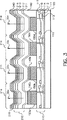
図2は、本発明によるデバイスの1画素の断面図を示す。このデバイスは例えば、3つのガモット・サブ画素21a、21b及び21c、及び1つのガモット内サブ画素21dを備えたストライプ・パターンを有する。これらのサブ画素は、ガモット色を有する光30a、30b及び30cを発し、そしてガモット内色を有する光30dを発する。図2に示されたデバイスは、アクティブ・マトリックス回路110を有するアクティブ・マトリックスであることが示されているが、しかしアクティブ・マトリックス回路を有しないパッシブ・マトリックスである別の実施態様を本発明に適用することもできる。図2はまた、底部発光型の形態、すなわち、基板の方向において光(30a、30b、30c及び30d)が抽出される形態を示している。ガモット・サブ画素21a、21b及び21cは、マイクロキャビティ構造を使用して形成される。マイクロキャビティ構造は、リフレクター及び半透明リフレクターを使用して形成される。有機EL媒質は、リフレクターと半透明リフレクターとの間に形成される。リフレクターと半透明リフレクターとの間の層は、光キャビティを形成する。この場合、光キャビティは所望の波長で共鳴するように、厚さ及び屈折率で調節される。マイクロキャビティ構造の例は、米国特許第6,406,801号明細書、同第5,780,174号明細書、及びJP第11288786号に示されている。高反射性のリフレクターのための好ましい材料は、Ag、Al、Au又はこれらの材料のうちの1種又は2種以上から成る合金を含む。半透明リフレクターは部分反射性であり、且つ部分透過性である。半透明リフレクターの好ましい材料は、Ag、Au、これらの材料のうちの一方又は両方から成る合金を含む。これらの材料の厚さは、材料を半透明にさせる、すなわち部分透過性且つ部分反射性にさせるように選択されている。この厚さは例えば5 nm〜50 nm、そして好ましくは15 nm〜30 nmであってよい。リフレクター又は半透明リフレクターを形成するために導電性材料が使用される場合、リフレクター、半透明リフレクター又はその両方が、有機EL媒質のための電極の機能、つまりアノード又はカソードの機能を果たすこともできる。高屈折率と低屈折率とを交互に有する透明材料の4分の1波長スタック(QWS)から成る別の半透明リフレクター構造も知られており、当業者によって本発明に適用することができる。光が基板を通して見られる図示のような底部発光形態において、半透明リフレクターは、有機EL層と基板との間に配置されており、そしてリフレクターは、基板、半透明リフレクター及び有機EL層の上方に配置されている。或いは、上部発光形態の場合、すなわち光が基板とは反対の方向で見られる場合、リフレクターは、有機EL層と基板との間に配置されており、そして半透明リフレクターは、基板、リフレクター及び有機EL層の上方に配置されている。
FIG. 2 shows a cross-sectional view of one pixel of a device according to the invention. This device has, for example, a stripe pattern with three gamut sub-pixels 21a, 21b and 21c and one in-
アクティブ・マトリックス回路110は、基板100の上方に配置されている。アクティブ・マトリックス回路110は、半導体アクティブ層111と、ゲート誘電体112と、ゲート導体113と、第1絶縁層114と、第2絶縁層117とから成る第1の薄膜トランジスター(TFT)を含む。アクティブ・マトリックス回路110はさらに、輝度信号を運ぶ1つの信号線116と、トランジスターに給電するための1つの電力線115とを含む。TFT回路を製作する方法が当業者によく知られている。単独のトランジスター、信号線、及び電力線だけが画素毎に示されているが、典型的には、各サブ画素はまた、第2のトランジスター(図示せず)並びにキャパシター(図示せず)及び付加的な選択線(図示せず)を有する。種々異なる数及び形態の回路素子を有する多くのタイプの回路が当業者に知られており、いうまでもなく多種多様のこれらの回路が本発明とともに働くことになる。アクティブ・マトリックス形態の例は、米国特許第5,550,066号、同第6,281,634号、及び同第6,501,466号明細書を含む。図示のTFTは薄膜半導体アクティブ層111を用いて製作されているが、言うまでもなく、半導体基板を用いることにより、基板はこの機能を実際に果たすことができる。ゲート導体113とゲート誘電体112とが半導体アクティブ層111の上方に位置する上部ゲート構造が示されているが、しかし、底部ゲートとして知られる逆の構造を有するTFTを使用して有機ELデバイスを駆動できることも当業者に知られている。
The
アクティブ・マトリックス回路の上方には、半透明リフレクター120a、120b及び120cが、それぞれガモット・サブ画素21a、21b及び21c内に形成されている。これらの半透明リフレクター120a、120b及び120cは、反射金属、例えばAg、Au、Al及びこれらの合金から形成することができ、これらはまた半透明であるように薄く形成される。必ずしも必要というわけではないが、半透明リフレクターはまた、有機EL媒質のための電極の一方として役立つことが可能である。
Above the active matrix circuit,
ガモット内サブ画素21dは、半透明リフレクターを有してはおらず、その代わりに透明電極130だけを有している。透明電極130は典型的には、金属酸化物、例えばインジウム錫酸化物(ITO)、亜鉛錫酸化物(ZTO)、酸化錫(SnOx)、酸化インジウム(InOx)、酸化モリブデン(MoOx)、酸化テルリウム(TeOx)、酸化アンチモン(SbOx)、及び酸化亜鉛(ZnOx)から構成されている。透明電極130はまた、図示のように直接的に、又は中間導体を用いて、アクティブ・マトリックス素子に電気的に接続される。半透明リフレクターのない透明電極を使用する結果、マイクロキャビティ構造を有しないガモット内サブ画素が生じる。
The in-
ガモット・サブ画素21aの場合、半透明リフレクター120a上に、透明キャビティ・スペーサー層140aが形成されている。透明キャビティ・スペーサー層140aは、金属酸化物、例えばインジウム錫酸化物(ITO)、亜鉛錫酸化物(ZTO)、酸化錫(SnOx)、酸化インジウム(InOx)、酸化モリブデン(MoOx)、酸化テルリウム(TeOx)、酸化アンチモン(SbOx)、及び酸化亜鉛(ZnOx)から構成することができる。この場合、透明キャビティ・スペーサー層140aは、有機EL媒質210のための電極としても役立つので、透明キャビティ・スペーサー層140aは、アクティブ・マトリックス素子に電気的に接続されなければならない。このことは直接的に達成するか、又は、半透明リフレクター120aが導電性材料、例えばAg、Al、Au又はこれらの合金から成る場合には、図示のような半透明リフレクター120aを介して、又は他の中間導体を用いて達成することができる。透明キャビティ・スペーサー層140aが導電性ではない場合、半透明リフレクター120aが有機EL媒質210の電極として役立つことができ、従って半透明リフレクター120aはアクティブ・マトリックス回路110に接続されることになる。或いは、透明電極130、透明キャビティ・スペーサー層140a、及び半透明リフレクター120aは、3つ(又は4つ以上)の異なる層から形成することができる。この場合、透明電極は、アクティブ・マトリックス回路と電気的な接触状態にあるようになり、キャビティ・スペーサー層は、透明電極と半透明リフレクターとの間に位置することができる。透明キャビティ・スペーサー層140aの厚さ及び屈折率は、有機EL媒質210の厚さ及び屈折率との関連において最適化され、これにより、サブ画素21aの光の色、例えば赤に対して所望される波長で共鳴するようにキャビティが調整される。所望のマイクロキャビティ発光を達成するために厚さ及び屈折率を調整させることは、当業者によく知られている。
In the case of the
ガモット・サブ画素21bは、半透明リフレクター120b上のキャビティ・スペーサー層140bを使用して、同様に構成されている。この場合、キャビティ・スペーサー層140bの厚さ及び屈折率は、有機EL媒質210の厚さ及び屈折率との関連において最適化され、これにより、サブ画素21bの光の色、例えば緑に対して所望される異なる波長で共鳴するようにキャビティが調整される。
The
ガモット・サブ画素21cは、ここでは、キャビティ・スペーサー層を有しないものとして示されている。この場合、有機EL媒質210の厚さ及び屈折率だけが最適化され、これにより、サブ画素21cの光の色、例えば青に対して所望される異なる波長で共鳴するようにキャビティが調整される。有機EL媒質210が図示のように全てのサブ画素に共通である場合、有機EL媒質210は、このガモット・サブ画素に対してだけ最適化され、そしてその他のガモット・サブ画素は、それぞれのキャビティ・スペーサー層を使用して別個に調整される。この形態は、デポジットされパターニングされるのを必要とする異なるキャビティ・スペーサー層の数を最小限に抑える。しかし、別の実施態様の場合、全てのガモット・サブ画素が、所望の色に調整されるようにそれぞれが別個に最適化されたキャビティ・スペーサー層を含むこともできる。これらの上記キャビティ・スペーサー層は、有機EL媒質210が、サブ画素毎のパターニングなしにデポジットされることを可能にするために使用されることが好ましい。しかし、別の実施態様の場合、有機EL媒質の有機層のうちの1つ又は2つ以上をパターニングし、厚さ又は屈折率を別個に調節することにより、ガモット・サブ画素のそれぞれのマイクロキャビティを調整させることもできる。この形態の場合、キャビティ・スペーサー層は使用することも排除することもできる。しかしこの形態は、有機層のうちの1つ以上の精密なパターニングを必要とする。
The
上述のように、デポジション工程及びパターニング工程の数を最小限に抑えるために、ガモット・サブ画素のうちの1つは、キャビティ・スペーサー層を有さなくてよい。デポジション工程及びパターニング工程の数を低減するための別の好ましい方法は、同じ材料、厚さ、及び屈折率を用いることにより、キャビティ・スペーサー層のうちの1つ、例えばキャビティ・スペーサー層140bと、非ガモット・サブ画素の透明電極、例えば透明電極130とを形成することである。
As described above, one of the gamut subpixels may not have a cavity spacer layer in order to minimize the number of deposition and patterning steps. Another preferred method for reducing the number of deposition and patterning steps is to use one of the cavity spacer layers, such as
米国特許第6,246,179号明細書に記載されているように、画素間誘電体層160を使用して、透明電極のエッジをカバーすることにより、この領域内の短絡又は強電界を防止することが好ましい。キャビティ・スペーサーが導電性であるか又は電極の一部を形成する場合、図示のように画素間誘電体層160は、キャビティ・スペーサーをカバーすることもできる。画素間誘電体層160の使用は好ましくはあるが、本発明の実施の成功に必要なものではない。
As described in US Pat. No. 6,246,179, it is preferable to use an inter-pixel
サブ画素のそれぞれはさらに、有機EL媒質210を形成する有機層を含む。有機EL媒質210層には、本発明の実施を成功させることができる多数の形態がある。広帯域光又は白色光を発する有機EL媒質層の例は、例えば同一譲受人の欧州特許出願公開第1 187 235号明細書、米国特許出願公開第20020025419号明細書(同一譲受人)、欧州特許第1 182 244号明細書、米国特許第5,683,823号明細書(同一譲受人);同第5,503,910号明細書;同第5,405,709号明細書(同一譲受人)、及び同第5,283,182号明細書に記載されている。同一譲受人の欧州特許出願公開第1 187 235号明細書に示されているように、下記層、すなわち正孔注入層211、正孔注入層211上に配置され黄色スペクトル域内で発光するためのルブレン化合物でドーピングされた正孔輸送層212、正孔輸送層212上に配置された青色発光化合物でドーピングされた発光層213、及び発光層213上に配置された電子輸送層214を含むことにより、白色発光有機EL媒質を得ることができる。1種又は2種以上の種々異なるEL媒質材料が種々異なるサブ画素のために使用される別の実施態様を、本発明に適用することもできる。
Each of the sub-pixels further includes an organic layer that forms the
有機EL媒質210上に、リフレクター220は形成される。リフレクター220は、Al、Ag、Au又はこれらの合金のような材料から形成することができる。リフレクター220は、有機EL媒質210のための第2の電極として役立つこともできる。
A
透明キャビティ・スペーサーは、ここでは半透明リフレクターと有機EL媒質との間に位置するものとして示されているが、別の実施態様の場合、代わりに有機EL媒質とリフレクターとの間に、キャビティ・ステップ・スペーサーを形成することもできる。 The transparent cavity spacer is shown here as being located between the translucent reflector and the organic EL medium, but in another embodiment, instead of between the organic EL medium and the reflector, the cavity Step spacers can also be formed.
有機EL媒質210の層のうちの1つ又は2つ以上が全てのサブ画素に共通するのではなく、その代わりにサブ画素毎に個々にパターニングされている別の実施態様の場合、キャビティ・スペーサー層を排除することができ、或いは、ガモット・サブ画素毎に別個に、有機EL媒質210を形成する層のうちの1つ又は2つ以上の厚さ、屈折率、又はその両方を調整することにより、ガモット・サブ画素のマイクロキャビティを調整することができる。この事例において、有機EL媒質210が広帯域光を発するように構成されている場合、ガモット内サブ画素のための有機EL媒質210層のうちの1つ又は2つ以上、及びガモット・サブ画素のうちの1つ又は2つ以上に対して同じ厚さを用いることにより、デポジション工程の数を最小限に抑えることが好ましい。 In another embodiment, where one or more of the layers of the organic EL medium 210 are not common to all subpixels, but instead are individually patterned for each subpixel, the cavity spacer Layers can be eliminated, or the thickness, refractive index, or both of one or more of the layers forming the organic EL medium 210 can be adjusted separately for each gamut subpixel Thus, the microcavity of the gamut subpixel can be adjusted. In this case, if the organic EL medium 210 is configured to emit broadband light, one or more of the organic EL medium 210 layers for the sub-pixel in the gamut, and of the gamut sub-pixel It is preferable to minimize the number of deposition steps by using the same thickness for one or more of the layers.
図3は、基板から遠ざかる方向で光(30a、30b、30c及び30d)が抽出される上部発光型の本発明の別の実施態様の断面図を示す。この上部発光形態を実現するために、有機EL媒質210と基板100との間に、リフレクター150a、150b、150c及び150dが配置されている。これらのリフレクター150a、150b、150c及び150dは、Ag、Au、Al又はこれらの合金のような材料から形成することができる。これらのリフレクター150a、150b、150c及び150dは、図示の有機EL媒質210のための電極として役立つこともでき、この場合、電極はアクティブ・マトリックス回路に接続されなければならない。この実施態様の場合、半透明リフレクター230は、ガモット・サブ画素21a、21b及び21cのための有機EL媒質210の上方に形成されなければならない。しかし、半透明リフレクター230は、ガモット内サブ画素21d内には存在しないようにパターニングされなければならない。ガモット内サブ画素21d上には、透明電極24が使用されなければならない。透明電極が図示のように他のサブ画素上にも存在することにより、パターニングの必要を低減することができるが、このことは必ずしも必要でない。透明電極240は金属酸化物、例えばインジウム錫酸化物(ITO)、亜鉛錫酸化物(ZTO)、酸化錫(SnOx)、酸化インジウム(InOx)、酸化モリブデン(MoOx)、酸化テルリウム(TeOx)、酸化アンチモン(SbOx)、及び酸化亜鉛(ZnOx)から構成することができる。
FIG. 3 shows a cross-sectional view of another embodiment of the present invention of top emission type in which light (30a, 30b, 30c and 30d) is extracted in a direction away from the substrate. In order to realize this upper light emission mode,
図3の場合、リフレクター(150a、150b、150c及び150d)が有機EL媒質210のための1つの電極を形成しているが、別の実施態様の場合、リフレクターの上、そして有機EL媒質210の下に、別個の電極を形成することができ、この場合、電極は、ガモット・サブ画素21a、21b及び21cのためのマイクロキャビティの一部になる。この電極は金属酸化物、例えばインジウム錫酸化物(ITO)、亜鉛錫酸化物(ZTO)、酸化錫(SnOx)、酸化インジウム(InOx)、酸化モリブデン(MoOx)、酸化テルリウム(TeOx)、酸化アンチモン(SbOx)、及び酸化亜鉛(ZnOx)から構成することができる。
In the case of FIG. 3, the reflectors (150a, 150b, 150c and 150d) form one electrode for the organic EL medium 210, but in another embodiment, on the reflector and on the
透明電極240は図3では、半透明リフレクター230上に位置しているものとして示されているが、別の実施態様の場合、透明電極240は半透明リフレクター230と有機EL媒質210との間に配置することができる。この場合、透明電極240は、サブ画素全てに対する有機EL媒質210のための電極の一方を形成し、そしてマイクロキャビティの一部になる。
Although the
上記の実施態様は、ガモット内サブ画素から広帯域又は白色の発光を生じさせる能力を維持しつつ、マイクロキャビティを使用することにより全てのガモット・サブ画素の効率及び耐用寿命が改善された例を示している。しかし、ガモット・サブ画素のいくつかだけがマイクロキャビティ構造を使用することにより改善される他の実施態様が可能である。すなわち、ガモット・サブ画素のいくつかは、マイクロキャビティを形成するようには構成されない。図4に示されたこのような形態の一例は、2つのマイクロキャビティ・ガモット・サブ画素22b及び22cと、1つの非マイクロキャビティ・ガモット・サブ画素22aと、ガモット内サブ画素22dとを有する。この事例において、非マイクロキャビティ・ガモット・サブ画素22aは、リフレクター220と透明電極130aとを使用して形成される。透明電極は、ガモット内サブ画素22dの透明電極130dのために用いられるのと同じ材料及び厚さを有することができる。使用される有機EL媒質210が、白色又は広帯域発光型である場合には、カラーフィルタ301を使用することにより、これらのサブ画素の所望のガモット色を達成することができる。広帯域発光を特定色の狭帯域発光に変換するためにカラーフィルタを使用することは当業者に知られている。ガモット・サブ画素のうちの1つ以上がマイクロキャビティとして構成される限り、耐用寿命及び効率の何らかの改善が本発明により実現されることになる。
The above embodiment shows an example where the efficiency and useful life of all gamut sub-pixels are improved by using a microcavity while maintaining the ability to produce broadband or white light emission from the sub-pixel in the gamut. ing. However, other embodiments are possible where only some of the gamut subpixels are improved by using a microcavity structure. That is, some of the gamut subpixels are not configured to form a microcavity. An example of such a configuration shown in FIG. 4 has two
或る好ましい実施態様を具体的に参照しながら本発明を説明してきたが、本発明の思想及び範囲内で、変更や改変を加えることができるのは言うまでもない。 Although the invention has been described with specific reference to certain preferred embodiments, it will be understood that changes and modifications may be made within the spirit and scope of the invention.
20 画素
21a ガモット・サブ画素
21b ガモット・サブ画素
21c ガモット・サブ画素
21d ガモット内サブ画素
22a 非マイクロキャビティ・ガモット・サブ画素
22b マイクロキャビティ・ガモット・サブ画素
22c マイクロキャビティ・ガモット・サブ画素
22d ガモット内サブ画素
30a 光
30b 光
30c 光
30d 光
100 基板
110 アクティブ・マトリックス回路
111 半導体アクティブ層
112 ゲート誘電体
113 ゲート導体
114 第1絶縁層
115 電力線
116 信号線
117 第2絶縁層
120a 半透明リフレクター
120b 半透明リフレクター
120c 半透明リフレクター
130 透明電極
130a 透明電極
130d 透明電極
140a 透明キャビティ・スペーサー層
140b 透明キャビティ・スペーサー層
150a リフレクター
150b リフレクター
150c リフレクター
150d リフレクター
160 画素間誘電体
210 正孔注入層
212 正孔輸送層
213 発光層
214 電子輸送層
220 リフレクター
230 半透明リフレクター
240 透明電極
310 カラーフィルター
20 pixels
21a gamut subpixel
21b gamut subpixel
21c gamut subpixel
21d Sub-pixel in gamut
22a Non-microcavity gamut subpixel
22b Microcavity Gamut Subpixel
22c microcavity gamut subpixel
22d Sub-pixel in gamut
30a light
30b light
30c light
30d light
100 substrates
110 active matrix circuit
111 Semiconductor active layer
112 Gate dielectric
113 Gate conductor
114 First insulation layer
115 Power line
116 Signal line
117 Second insulation layer
120a translucent reflector
120b translucent reflector
120c translucent reflector
130 Transparent electrode
130a transparent electrode
130d transparent electrode
140a transparent cavity spacer layer
140b Transparent cavity spacer layer
150a reflector
150b reflector
150c reflector
150d reflector
160 Inter-pixel dielectric
210 Hole injection layer
212 Hole transport layer
213 Light emitting layer
214 Electron transport layer
220 reflector
230 Translucent reflector
240 transparent electrode
310 Color filter
Claims (4)
(a)発光画素アレイを含み、各画素が、光を生成する1つ以上の発光層を含む有機層と、離間した電極とを有するサブ画素を含み、そして、色ガモットを画定する色を生成する3つ以上のガモット・サブ画素と、該ガモット・サブ画素によって生成される色ガモット内の光を生成する1つ以上のサブ画素とがあり;そして
(b)該ガモット・サブ画素のうちの1つ以上が、マイクロキャビティを形成する機能を発揮するリフレクターと半透明リフレクターとを含み、
マイクロキャビティ構造を有する該ガモット・サブ画素はさらに、透明キャビティ・スペーサー層を含み、該透明キャビティ・スペーサー層の厚さ、該透明キャビティ・スペーサー層の屈折率、又はその両方を、ガモット・サブ画素毎の有機層の厚さ及び屈折率との関連において、異なる色のガモット・サブ画素毎に別個に調節することにより、マイクロキャビティを所望の色に調整し、
該ガモット・サブ画素のうちの1つの該透明キャビティ・スペーサー層が、該ガモット内サブ画素のうちの1つ以上の透明電極と同じ材料及び厚さから形成されており、
該ガモット内サブ画素は、半透明リフレクターを有しない、OLEDデバイス。OLED device:
(a) includes a luminescent pixel array, each pixel including a sub-pixel having an organic layer including one or more luminescent layers that generate light, and spaced electrodes, and generates a color that defines a color gamut Three or more gamut sub-pixels, and one or more sub-pixels that generate light in the color gamut generated by the gamut sub-pixels; and
(b) at least one of the gamut sub-pixels includes a reflector that functions to form a microcavity and a translucent reflector;
The gamut subpixel having a microcavity structure further includes a transparent cavity spacer layer, and the thickness of the transparent cavity spacer layer, the refractive index of the transparent cavity spacer layer, or both are determined by the gamut subpixel. Adjust the microcavity to the desired color by adjusting separately for each different color gamut sub-pixel in relation to the thickness and refractive index of each organic layer,
The transparent cavity spacer layer of one of the gamut sub-pixels is formed of the same material and thickness as one or more transparent electrodes of the in-gamut sub-pixels ;
The sub-pixel in the gamut does not have a translucent reflector, OLED device.
(a)発光画素アレイを含み、各画素が、光を生成する1つ以上の発光層を含む有機層と、離間した電極とを有するサブ画素を含み、そして、色ガモットを画定する色を生成する3つ以上のガモット・サブ画素と、該ガモット・サブ画素によって生成される色ガモット内の光を生成する1つ以上のサブ画素とがあり;そして
(b)該ガモット・サブ画素のうちの1つ以上が、マイクロキャビティを形成する機能を発揮するリフレクターと半透明リフレクターとを含み、
マイクロキャビティ構造を有する該ガモット・サブ画素のうちの1つを除く全てがさらに、透明キャビティ・スペーサー層を含み、該透明キャビティ・スペーサー層の厚さ、該透明キャビティ・スペーサー層の屈折率、又はその両方を、ガモット・サブ画素毎の有機層の厚さ及び屈折率との関連において、異なる色のガモット・サブ画素毎に別個に調節することにより、マイクロキャビティを所望の色に調整し、
該ガモット・サブ画素のうちの1つの該透明キャビティ・スペーサー層が、該ガモット内サブ画素のうちの1つ以上の透明電極と同じ材料及び厚さから形成されており、
該ガモット内サブ画素は、半透明リフレクターを有しない、OLEDデバイス。OLED device:
(a) includes a luminescent pixel array, each pixel including a sub-pixel having an organic layer including one or more luminescent layers that generate light, and spaced electrodes, and generates a color that defines a color gamut Three or more gamut sub-pixels, and one or more sub-pixels that generate light in the color gamut generated by the gamut sub-pixels; and
(b) at least one of the gamut sub-pixels includes a reflector that functions to form a microcavity and a translucent reflector;
All but one of the gamut subpixels having a microcavity structure further comprise a transparent cavity spacer layer, the thickness of the transparent cavity spacer layer, the refractive index of the transparent cavity spacer layer, or Adjust the microcavity to the desired color by adjusting both separately in relation to the thickness and refractive index of the organic layer for each gamut subpixel, for each gamut subpixel of a different color,
The transparent cavity spacer layer of one of the gamut sub-pixels is formed of the same material and thickness as one or more transparent electrodes of the in-gamut sub-pixels ;
The sub-pixel in the gamut does not have a translucent reflector, OLED device.
Applications Claiming Priority (3)
| Application Number | Priority Date | Filing Date | Title |
|---|---|---|---|
| US10/643,837 US7030553B2 (en) | 2003-08-19 | 2003-08-19 | OLED device having microcavity gamut subpixels and a within gamut subpixel |
| US10/643,837 | 2003-08-19 | ||
| PCT/US2004/025741 WO2005020344A1 (en) | 2003-08-19 | 2004-08-09 | Oled device having microcavity gamut subpixels |
Publications (3)
| Publication Number | Publication Date |
|---|---|
| JP2007503093A JP2007503093A (en) | 2007-02-15 |
| JP2007503093A5 JP2007503093A5 (en) | 2007-09-20 |
| JP4741492B2 true JP4741492B2 (en) | 2011-08-03 |
Family
ID=34193971
Family Applications (1)
| Application Number | Title | Priority Date | Filing Date |
|---|---|---|---|
| JP2006523907A Active JP4741492B2 (en) | 2003-08-19 | 2004-08-09 | OLED device with microcavity gamut subpixel |
Country Status (5)
| Country | Link |
|---|---|
| US (1) | US7030553B2 (en) |
| JP (1) | JP4741492B2 (en) |
| KR (1) | KR101069235B1 (en) |
| CN (1) | CN100459144C (en) |
| WO (1) | WO2005020344A1 (en) |
Families Citing this family (169)
| Publication number | Priority date | Publication date | Assignee | Title |
|---|---|---|---|---|
| US6872472B2 (en) * | 2002-02-15 | 2005-03-29 | Eastman Kodak Company | Providing an organic electroluminescent device having stacked electroluminescent units |
| JP4716699B2 (en) * | 2003-09-30 | 2011-07-06 | 三洋電機株式会社 | Organic EL panel |
| JP4428979B2 (en) * | 2003-09-30 | 2010-03-10 | 三洋電機株式会社 | Organic EL panel |
| JP4497881B2 (en) | 2003-09-30 | 2010-07-07 | 三洋電機株式会社 | Organic EL device and organic EL panel |
| JP4895490B2 (en) * | 2003-09-30 | 2012-03-14 | 三洋電機株式会社 | Organic EL panel |
| US20050116615A1 (en) * | 2003-09-30 | 2005-06-02 | Shoichiro Matsumoto | Light emissive display device |
| TW200515836A (en) * | 2003-10-22 | 2005-05-01 | Hannstar Display Corp | Organic electroluminescent element |
| JP3994994B2 (en) * | 2003-10-23 | 2007-10-24 | セイコーエプソン株式会社 | Organic EL device manufacturing method, organic EL device, and electronic apparatus |
| KR100527198B1 (en) * | 2003-11-12 | 2005-11-08 | 삼성에스디아이 주식회사 | flat panel display for displaying screens at both sides |
| KR100611157B1 (en) * | 2003-11-29 | 2006-08-09 | 삼성에스디아이 주식회사 | organic light-emitting device and fabrication method of the same |
| US8796670B2 (en) | 2003-12-26 | 2014-08-05 | Semiconductor Energy Laboratory Co., Ltd. | Light-emitting element |
| JP4439260B2 (en) * | 2003-12-26 | 2010-03-24 | 三洋電機株式会社 | Manufacturing method of display device |
| JP4475942B2 (en) | 2003-12-26 | 2010-06-09 | 三洋電機株式会社 | Display device and manufacturing method thereof |
| WO2005086539A1 (en) * | 2004-03-05 | 2005-09-15 | Idemitsu Kosan Co., Ltd. | Organic electroluminescence display device |
| KR100579192B1 (en) * | 2004-03-11 | 2006-05-11 | 삼성에스디아이 주식회사 | Top-emission type organic electro luminescence display device and method for fabricating of the same |
| JP4454354B2 (en) * | 2004-03-25 | 2010-04-21 | 三洋電機株式会社 | Luminescent display device |
| JP4143569B2 (en) * | 2004-05-14 | 2008-09-03 | キヤノン株式会社 | Color display device |
| KR100755398B1 (en) * | 2004-05-21 | 2007-09-04 | 엘지전자 주식회사 | Organic Electro-luminescence Display Device and Method For Fabricating Thereof |
| KR100704258B1 (en) * | 2004-06-02 | 2007-04-06 | 세이코 엡슨 가부시키가이샤 | Organic el device and electronic apparatus |
| TWI272039B (en) | 2004-06-18 | 2007-01-21 | Sanyo Electric Co | Electroluminescence panel |
| US7196469B2 (en) * | 2004-06-18 | 2007-03-27 | Eastman Kodak Company | Reducing undesirable absorption in a microcavity OLED |
| JP4239983B2 (en) * | 2004-07-13 | 2009-03-18 | セイコーエプソン株式会社 | Organic EL device |
| US7601988B2 (en) | 2004-09-24 | 2009-10-13 | Semiconductor Energy Laboratory Co., Ltd. | Light emitting device |
| KR101122229B1 (en) * | 2004-10-05 | 2012-03-19 | 삼성전자주식회사 | Four color liquid crystal display |
| KR100579186B1 (en) * | 2004-10-15 | 2006-05-11 | 삼성에스디아이 주식회사 | Organic electroluminescence display device |
| TWI339835B (en) | 2005-02-03 | 2011-04-01 | Chimei Innolux Corp | Pixel structure for a color display device, organic light emitting device module, electronic device and method of rendering color of a pixel in a display device |
| JP4573672B2 (en) | 2005-02-28 | 2010-11-04 | 三洋電機株式会社 | Organic EL panel |
| US7190122B2 (en) * | 2005-03-01 | 2007-03-13 | Eastman Kodak Company | OLED display with improved active matrix circuitry |
| JP2006253015A (en) * | 2005-03-11 | 2006-09-21 | Idemitsu Kosan Co Ltd | Organic electroluminescence color light-emitting device |
| TWI282699B (en) * | 2005-03-14 | 2007-06-11 | Au Optronics Corp | Method of fabrication organic light emitting diode display |
| JP4830328B2 (en) * | 2005-03-25 | 2011-12-07 | セイコーエプソン株式会社 | Light emitting device |
| US7851989B2 (en) * | 2005-03-25 | 2010-12-14 | Semiconductor Energy Laboratory Co., Ltd. | Light emitting device |
| JP5072243B2 (en) * | 2005-03-25 | 2012-11-14 | 株式会社半導体エネルギー研究所 | Light emitting device |
| JP4742639B2 (en) * | 2005-03-25 | 2011-08-10 | セイコーエプソン株式会社 | Light emitting device |
| KR100729060B1 (en) * | 2005-03-31 | 2007-06-14 | 삼성에스디아이 주식회사 | Light Emitting Display and Driving Method Thereof |
| US7271537B2 (en) * | 2005-04-15 | 2007-09-18 | Sony Corporation | Display device and a method of manufacturing the display device |
| JP4507964B2 (en) * | 2005-04-15 | 2010-07-21 | ソニー株式会社 | Display device and manufacturing method of display device |
| JP4876453B2 (en) * | 2005-06-29 | 2012-02-15 | ソニー株式会社 | Organic light emitting device and organic light emitting device |
| US7564182B2 (en) * | 2005-06-29 | 2009-07-21 | Eastman Kodak Company | Broadband light tandem OLED display |
| US7531959B2 (en) * | 2005-06-29 | 2009-05-12 | Eastman Kodak Company | White light tandem OLED display with filters |
| WO2007004106A1 (en) * | 2005-06-30 | 2007-01-11 | Koninklijke Philips Electronics N.V. | Light-emitting device |
| US8729795B2 (en) | 2005-06-30 | 2014-05-20 | Semiconductor Energy Laboratory Co., Ltd. | Light emitting device and electronic device |
| JP4197000B2 (en) * | 2005-07-07 | 2008-12-17 | エプソンイメージングデバイス株式会社 | Electro-optical device and electronic apparatus |
| US8102111B2 (en) * | 2005-07-15 | 2012-01-24 | Seiko Epson Corporation | Electroluminescence device, method of manufacturing electroluminescence device, and electronic apparatus |
| TWI262038B (en) * | 2005-08-12 | 2006-09-11 | Au Optronics Corp | Pixel structure and organic electroluminescent panel with the structure |
| TWI326379B (en) * | 2005-09-20 | 2010-06-21 | Au Optronics Corp | A double-sided liquid crystal display |
| US20070063192A1 (en) * | 2005-09-20 | 2007-03-22 | Toppoly Optoelectronics Corp. | Systems for emitting light incorporating pixel structures of organic light-emitting diodes |
| EP2472507B1 (en) | 2005-10-14 | 2016-02-10 | Samsung Display Co., Ltd. | Improved gamut mapping and subpixel rendering systems and methods |
| US7742205B2 (en) * | 2005-12-16 | 2010-06-22 | Vp Assets Limited Registered In British Virgin Islands | Perceptual color matching method between two different polychromatic displays |
| JP2007179828A (en) * | 2005-12-27 | 2007-07-12 | Fujifilm Corp | Organic electroluminescent element and method of manufacturing same |
| JP4678319B2 (en) * | 2006-03-15 | 2011-04-27 | セイコーエプソン株式会社 | LIGHT EMITTING DEVICE AND ELECTRONIC DEVICE |
| US7888860B2 (en) * | 2006-08-25 | 2011-02-15 | Samsung Electronics Co., Ltd. | Organic light emitting device |
| JP4816354B2 (en) * | 2006-09-15 | 2011-11-16 | セイコーエプソン株式会社 | Electro-optical device and electronic apparatus |
| KR101350658B1 (en) * | 2006-09-22 | 2014-01-10 | 엘지디스플레이 주식회사 | Organic electro-luminescence display device and method of maunfacturing the same |
| KR100823511B1 (en) * | 2006-11-10 | 2008-04-21 | 삼성에스디아이 주식회사 | Organic light emission display and fabrication method thereof |
| JP2008170756A (en) | 2007-01-12 | 2008-07-24 | Sony Corp | Display device |
| JP4479737B2 (en) * | 2007-03-07 | 2010-06-09 | セイコーエプソン株式会社 | LIGHT EMITTING DEVICE, ITS MANUFACTURING METHOD, AND ELECTRONIC DEVICE |
| JP4529988B2 (en) * | 2007-03-08 | 2010-08-25 | セイコーエプソン株式会社 | Light emitting device and electronic device |
| JP4582102B2 (en) * | 2007-03-08 | 2010-11-17 | セイコーエプソン株式会社 | LIGHT EMITTING DEVICE, ITS MANUFACTURING METHOD, AND ELECTRONIC DEVICE |
| TWI359626B (en) * | 2007-03-22 | 2012-03-01 | Au Optronics Corp | Electro-luminescence display |
| US8183767B2 (en) * | 2007-07-06 | 2012-05-22 | Canon Kabushiki Kaisha | Display apparatus and imaging system using the same |
| US7859188B2 (en) * | 2007-08-21 | 2010-12-28 | Global Oled Technology Llc | LED device having improved contrast |
| US7888858B2 (en) * | 2007-08-21 | 2011-02-15 | Global Oled Technology Llc | Light emitting diode device incorporating a white light emitting layer in combination with a plurality of optical microcavities |
| US7855508B2 (en) * | 2007-09-17 | 2010-12-21 | Global Oled Technology Llc | LED device having improved light output |
| US7948172B2 (en) * | 2007-09-28 | 2011-05-24 | Global Oled Technology Llc | LED device having improved light output |
| US7741770B2 (en) * | 2007-10-05 | 2010-06-22 | Global Oled Technology Llc | LED device having improved light output |
| US8063552B2 (en) * | 2007-10-22 | 2011-11-22 | Global Oled Technology Llc | LED device having improved light output |
| US8076838B2 (en) * | 2007-10-31 | 2011-12-13 | Seiko Epson Corporation | Light emitting device |
| FR2925746B1 (en) * | 2007-12-21 | 2010-01-01 | Commissariat Energie Atomique | DISPLAY DEVICE COMPRISING COLOR FILTERS AND ELECTRONICALLY ALIGNED PHOTOEMISSIVE ELEMENTS |
| FR2926677B1 (en) * | 2008-01-18 | 2014-04-25 | Astron Fiamm Safety | DIODE AND METHOD FOR PRODUCING A MICROCAVITY ORGANIC ELECTROLUMINESCENT DIODE INCLUDING DOPED ORGANIC LAYERS |
| US8013516B2 (en) * | 2008-01-23 | 2011-09-06 | Global Oled Technology Llc | LED device having improved power distribution |
| KR101458908B1 (en) * | 2008-04-01 | 2014-11-07 | 삼성디스플레이 주식회사 | Organic light emitting diode display and method for manufacturing the same |
| KR20090089151A (en) * | 2008-02-18 | 2009-08-21 | 삼성전자주식회사 | Organic light emitting diode display and method for manufacturing the same |
| US7973470B2 (en) | 2008-02-26 | 2011-07-05 | Global Oled Technology Llc | Led device having improved color |
| US7893612B2 (en) * | 2008-02-27 | 2011-02-22 | Global Oled Technology Llc | LED device having improved light output |
| KR101448003B1 (en) * | 2008-04-04 | 2014-10-08 | 삼성디스플레이 주식회사 | Organic light emitting diode display and method for manufacturing the same |
| KR101469031B1 (en) * | 2008-04-16 | 2014-12-05 | 삼성디스플레이 주식회사 | Organic light emitting devicce |
| KR100909389B1 (en) * | 2008-04-21 | 2009-07-24 | 삼성모바일디스플레이주식회사 | Organic light emitting diode display device |
| KR20090112088A (en) * | 2008-04-23 | 2009-10-28 | 삼성전자주식회사 | Organic light emitting device and manufacturing method thereof |
| US8193695B2 (en) * | 2008-07-17 | 2012-06-05 | Samsung Electronics Co., Ltd. | Organic light emitting device and manufacturing method thereof |
| KR101518740B1 (en) * | 2008-08-04 | 2015-05-11 | 삼성디스플레이 주식회사 | Organic light emitting device and manufacturing method thereof |
| JP5117326B2 (en) * | 2008-08-29 | 2013-01-16 | 富士フイルム株式会社 | Color display device and manufacturing method thereof |
| KR101574130B1 (en) * | 2008-09-01 | 2015-12-04 | 삼성디스플레이 주식회사 | Organic light emitting diode display and method for manufacturing the same |
| US9385167B2 (en) | 2008-10-01 | 2016-07-05 | Universal Display Corporation | OLED display architecture |
| US20100225252A1 (en) | 2008-10-01 | 2010-09-09 | Universal Display Corporation | Novel amoled display architecture |
| US8022612B2 (en) * | 2008-11-10 | 2011-09-20 | Global Oled Technology, Llc. | White-light LED having two or more commonly controlled portions with improved angular color performance |
| KR101649224B1 (en) * | 2008-12-16 | 2016-08-18 | 엘지디스플레이 주식회사 | Top Emission White Organic Light Emitting Display Device |
| JP2010232163A (en) | 2009-03-03 | 2010-10-14 | Fujifilm Corp | Method of manufacturing light-emitting display device, light-emitting display device, and light-emitting display |
| KR101116825B1 (en) * | 2009-08-06 | 2012-02-29 | 엘지디스플레이 주식회사 | Organic Light Emitting Diode Display Device |
| KR101094298B1 (en) * | 2009-08-18 | 2011-12-19 | 삼성모바일디스플레이주식회사 | Organic light emitting diode display |
| KR101321878B1 (en) * | 2009-09-25 | 2013-10-28 | 엘지디스플레이 주식회사 | Organic electro luminescent device |
| KR101084177B1 (en) * | 2009-11-30 | 2011-11-17 | 삼성모바일디스플레이주식회사 | OLED display apparatus and Method thereof |
| KR101108167B1 (en) * | 2010-02-12 | 2012-02-06 | 삼성모바일디스플레이주식회사 | Organic light emitting display apparatus |
| KR101084196B1 (en) * | 2010-02-19 | 2011-11-17 | 삼성모바일디스플레이주식회사 | Organic light emitting display apparatus |
| US8334545B2 (en) * | 2010-03-24 | 2012-12-18 | Universal Display Corporation | OLED display architecture |
| JP5670178B2 (en) | 2010-12-28 | 2015-02-18 | ユー・ディー・シー アイルランド リミテッド | Organic electroluminescence device |
| KR101894898B1 (en) | 2011-02-11 | 2018-09-04 | 가부시키가이샤 한도오따이 에네루기 켄큐쇼 | Light-emitting device and electronic device using light-emitting device |
| JP2012204164A (en) * | 2011-03-25 | 2012-10-22 | Sony Corp | Organic el display device and method for manufacturing the same |
| TWI562424B (en) | 2011-03-25 | 2016-12-11 | Semiconductor Energy Lab Co Ltd | Light-emitting panel, light-emitting device, and method for manufacturing the light-emitting panel |
| KR101784994B1 (en) * | 2011-03-31 | 2017-10-13 | 삼성디스플레이 주식회사 | Organic light emitting diode display and manufacturing method thereof |
| KR101960759B1 (en) | 2011-04-08 | 2019-03-21 | 가부시키가이샤 한도오따이 에네루기 켄큐쇼 | Light-emitting device, electronic appliance, and lighting device |
| KR101917752B1 (en) | 2011-05-11 | 2018-11-13 | 가부시키가이샤 한도오따이 에네루기 켄큐쇼 | Light-emitting element, light-emitting module, light-emmiting panel, and light-emitting device |
| JP2012252829A (en) * | 2011-06-01 | 2012-12-20 | Seiko Epson Corp | Manufacturing method for light-emitting device |
| WO2013008765A1 (en) | 2011-07-08 | 2013-01-17 | Semiconductor Energy Laboratory Co., Ltd. | Light-emitting module, light-emitting device, and method for manufacturing the light-emitting module |
| CN102270750A (en) * | 2011-07-26 | 2011-12-07 | 昆山维信诺显示技术有限公司 | Organic electroluminescent device, display equipment and manufacture method |
| KR101821739B1 (en) | 2011-08-25 | 2018-01-25 | 삼성디스플레이 주식회사 | Organic light emitting diode display and manufacturing method thereof |
| JP5927601B2 (en) * | 2011-09-07 | 2016-06-01 | 株式会社Joled | Luminescent panel, display device and electronic device |
| US9721998B2 (en) * | 2011-11-04 | 2017-08-01 | Semiconductor Energy Laboratory Co., Ltd. | Display device and driving method thereof |
| KR101407309B1 (en) * | 2011-11-15 | 2014-06-16 | 엘지디스플레이 주식회사 | Organic electro-luminesence display panel and manufacturing method of the same |
| GB201200823D0 (en) * | 2012-01-18 | 2012-02-29 | Cambridge Display Tech Ltd | Electroluminescence |
| US9065077B2 (en) | 2012-06-15 | 2015-06-23 | Apple, Inc. | Back channel etch metal-oxide thin film transistor and process |
| JP2014026902A (en) * | 2012-07-30 | 2014-02-06 | Sony Corp | Display device, method for manufacturing display device, and electronic apparatus |
| US8883531B2 (en) * | 2012-08-28 | 2014-11-11 | Lg Display Co., Ltd. | Organic light emitting diode display device and method of manufacturing the same |
| US8987027B2 (en) | 2012-08-31 | 2015-03-24 | Apple Inc. | Two doping regions in lightly doped drain for thin film transistors and associated doping processes |
| US9685557B2 (en) | 2012-08-31 | 2017-06-20 | Apple Inc. | Different lightly doped drain length control for self-align light drain doping process |
| US9000452B2 (en) | 2012-09-28 | 2015-04-07 | Industrial Technology Research Institute | Display with filter structure |
| US8999771B2 (en) | 2012-09-28 | 2015-04-07 | Apple Inc. | Protection layer for halftone process of third metal |
| US9201276B2 (en) | 2012-10-17 | 2015-12-01 | Apple Inc. | Process architecture for color filter array in active matrix liquid crystal display |
| CN103872068B (en) * | 2012-12-14 | 2017-04-26 | 京东方科技集团股份有限公司 | Variable-color light-emitting element, pixel structure and display device |
| JP6111643B2 (en) * | 2012-12-17 | 2017-04-12 | セイコーエプソン株式会社 | ORGANIC ELECTROLUMINESCENCE DEVICE AND ELECTRONIC DEVICE |
| KR101981071B1 (en) * | 2012-12-31 | 2019-05-22 | 엘지디스플레이 주식회사 | Organic Light Emitting Diode Display Device and Method for Manufacturing The Same |
| US20140203245A1 (en) * | 2013-01-24 | 2014-07-24 | Apple Inc. | Active Matrix Organic Light Emitting Diode Display Having Variable Optical Path Length for Microcavity |
| US9001297B2 (en) | 2013-01-29 | 2015-04-07 | Apple Inc. | Third metal layer for thin film transistor with reduced defects in liquid crystal display |
| US9088003B2 (en) * | 2013-03-06 | 2015-07-21 | Apple Inc. | Reducing sheet resistance for common electrode in top emission organic light emitting diode display |
| US9252375B2 (en) * | 2013-03-15 | 2016-02-02 | LuxVue Technology Corporation | Method of fabricating a light emitting diode display with integrated defect detection test |
| KR101978749B1 (en) * | 2013-05-13 | 2019-05-16 | 삼성디스플레이 주식회사 | Organic electroluminescent display |
| KR102054848B1 (en) * | 2013-06-04 | 2019-12-12 | 삼성디스플레이 주식회사 | Organic light emitting display apparatus and the manufacturing method thereof |
| KR102098068B1 (en) * | 2013-08-13 | 2020-04-07 | 엘지디스플레이 주식회사 | White organic light emitting diode display device using micro cavity |
| KR102094805B1 (en) * | 2013-10-15 | 2020-04-14 | 엘지디스플레이 주식회사 | organic light emitting diode display and method of fabricating the same |
| JP6488082B2 (en) * | 2013-12-02 | 2019-03-20 | 株式会社半導体エネルギー研究所 | LIGHT EMITTING DEVICE, ELECTRONIC DEVICE, AND LIGHTING DEVICE |
| KR102184939B1 (en) * | 2014-03-28 | 2020-12-02 | 엘지디스플레이 주식회사 | Organic Light Emitting Diode Display And Method For Manufacturing The Same |
| TWI567971B (en) * | 2014-04-22 | 2017-01-21 | 友達光電股份有限公司 | Light emitting device |
| CN113299711A (en) * | 2014-05-27 | 2021-08-24 | 环球展览公司 | High resolution low power OLED display with extended lifetime |
| US9874775B2 (en) * | 2014-05-28 | 2018-01-23 | Semiconductor Energy Laboratory Co., Ltd. | Liquid crystal display device and electronic device |
| TWI525379B (en) | 2014-06-04 | 2016-03-11 | 聯詠科技股份有限公司 | Display device and driving module thereof |
| US9455304B2 (en) * | 2014-06-26 | 2016-09-27 | Apple Inc. | Organic light-emitting diode display with white and blue diodes |
| US9269749B2 (en) * | 2014-07-07 | 2016-02-23 | Au Optronics Corporation | Organic electroluminescence display panel |
| KR102377360B1 (en) * | 2014-08-08 | 2022-03-21 | 가부시키가이샤 한도오따이 에네루기 켄큐쇼 | Light-emitting element, light-emitting device, lighting device, display device, display panel, and electronic appliance |
| KR102268135B1 (en) * | 2014-11-07 | 2021-06-23 | 삼성디스플레이 주식회사 | Organic light emitting diode display |
| JP5918340B2 (en) * | 2014-11-25 | 2016-05-18 | ユー・ディー・シー アイルランド リミテッド | Color display device and manufacturing method thereof |
| EP3236502A4 (en) * | 2014-12-18 | 2018-08-01 | Lg Electronics Inc. | Organic light-emitting diode display device |
| CN104538431B (en) * | 2014-12-31 | 2017-11-24 | 北京维信诺科技有限公司 | A kind of OLED and preparation method thereof, display |
| CN104600097A (en) * | 2015-02-06 | 2015-05-06 | 京东方科技集团股份有限公司 | Pixel unit structure, organic light emitting display panel and display device |
| WO2016127308A1 (en) * | 2015-02-10 | 2016-08-18 | 华为技术有限公司 | Display panel |
| KR102421582B1 (en) * | 2015-02-24 | 2022-07-18 | 삼성디스플레이 주식회사 | Organic light emitting display device and manufacturing method of the same |
| CN105206651B (en) | 2015-10-12 | 2019-01-04 | 深圳市华星光电技术有限公司 | A kind of OLED display panel and preparation method thereof |
| US10170521B2 (en) * | 2015-12-30 | 2019-01-01 | Lg Display Co., Ltd. | Organic light-emitting diode display device |
| CN105489632A (en) * | 2016-01-15 | 2016-04-13 | 京东方科技集团股份有限公司 | Organic light-emitting diode (OLED) array substrate, manufacturing method thereof, OLED display panel and OLED display device |
| US10797113B2 (en) | 2016-01-25 | 2020-10-06 | Semiconductor Energy Laboratory Co., Ltd. | Light-emitting device with layered electrode structures |
| CN105720081B (en) | 2016-02-24 | 2021-04-16 | 京东方科技集团股份有限公司 | Organic light-emitting diode array substrate, display device and manufacturing method |
| CN107275359B (en) | 2016-04-08 | 2021-08-13 | 乐金显示有限公司 | Organic light emitting display device |
| CN109315049B (en) * | 2016-05-11 | 2021-10-08 | 株式会社日本有机雷特显示器 | Display device and electronic apparatus |
| KR102569723B1 (en) * | 2016-05-13 | 2023-08-22 | 엘지디스플레이 주식회사 | White organic light emitting display device applying micro cavity |
| CN107634084B (en) * | 2017-09-13 | 2020-08-25 | 云谷(固安)科技有限公司 | Top-emitting white light OLED display device |
| KR102083459B1 (en) * | 2017-11-30 | 2020-03-04 | 엘지디스플레이 주식회사 | Display Device and Eyeglasses type Augmented Reality Device |
| JP2019114484A (en) * | 2017-12-26 | 2019-07-11 | ソニーセミコンダクタソリューションズ株式会社 | Display element and electronic device |
| CN108597386B (en) * | 2018-01-08 | 2020-12-29 | 京东方科技集团股份有限公司 | Color film, micro LED device, manufacturing method of micro LED device and display device |
| CN116347951A (en) * | 2018-05-11 | 2023-06-27 | 株式会社半导体能源研究所 | Display device, display module and electronic equipment |
| CN112088580A (en) * | 2018-05-15 | 2020-12-15 | 索尼半导体解决方案公司 | Display device, method for manufacturing display device, and electronic apparatus |
| CN112424969A (en) | 2018-05-18 | 2021-02-26 | 株式会社半导体能源研究所 | Light-emitting element, light-emitting device, electronic device, and lighting device |
| US11211587B2 (en) | 2018-07-30 | 2021-12-28 | Apple Inc. | Organic light-emitting diode display with structured electrode |
| FR3087582B1 (en) * | 2018-10-22 | 2021-09-03 | Microoled | DAY AND NIGHT DISPLAY DEVICE |
| CN109686768B (en) * | 2018-12-25 | 2021-04-30 | 武汉天马微电子有限公司 | Array substrate, preparation method thereof and display panel |
| US11903232B2 (en) | 2019-03-07 | 2024-02-13 | Semiconductor Energy Laboratory Co., Ltd. | Light-emitting device comprising charge-generation layer between light-emitting units |
| TWI691109B (en) * | 2019-05-09 | 2020-04-11 | 友達光電股份有限公司 | Display apparatus and manufacturing method thereof |
| CN110911463B (en) * | 2019-11-28 | 2023-01-10 | 京东方科技集团股份有限公司 | OLED display back plate, manufacturing method thereof and OLED display device |
| CN111223904B (en) * | 2019-12-20 | 2023-04-18 | 京东方科技集团股份有限公司 | Display panel and preparation method thereof, display device and control method thereof |
| KR20220018140A (en) * | 2020-08-05 | 2022-02-15 | 삼성디스플레이 주식회사 | Light emitting device and manufacturing method of the same |
| CN113328053A (en) * | 2021-05-20 | 2021-08-31 | 武汉华星光电技术有限公司 | Display panel |
Citations (3)
| Publication number | Priority date | Publication date | Assignee | Title |
|---|---|---|---|---|
| JPH06275831A (en) * | 1993-03-18 | 1994-09-30 | Hitachi Ltd | Thin-film transistor |
| JPH0992466A (en) * | 1995-09-20 | 1997-04-04 | Idemitsu Kosan Co Ltd | Organic electroluminescent element |
| JP2003178875A (en) * | 2001-12-11 | 2003-06-27 | Asahi Glass Co Ltd | Color organic el display |
Family Cites Families (25)
| Publication number | Priority date | Publication date | Assignee | Title |
|---|---|---|---|---|
| US4356429A (en) | 1980-07-17 | 1982-10-26 | Eastman Kodak Company | Organic electroluminescent cell |
| US5283182A (en) | 1986-09-17 | 1994-02-01 | Beecham Group Plc | Preparation of immobilized hydantoinase stabilized with divalent metal ions |
| US5276380A (en) | 1991-12-30 | 1994-01-04 | Eastman Kodak Company | Organic electroluminescent image display device |
| JP2797883B2 (en) | 1993-03-18 | 1998-09-17 | 株式会社日立製作所 | Multicolor light emitting device and its substrate |
| US5405709A (en) | 1993-09-13 | 1995-04-11 | Eastman Kodak Company | White light emitting internal junction organic electroluminescent device |
| US5503910A (en) | 1994-03-29 | 1996-04-02 | Idemitsu Kosan Co., Ltd. | Organic electroluminescence device |
| US5550066A (en) | 1994-12-14 | 1996-08-27 | Eastman Kodak Company | Method of fabricating a TFT-EL pixel |
| US5780174A (en) | 1995-10-27 | 1998-07-14 | Kabushiki Kaisha Toyota Chuo Kenkyusho | Micro-optical resonator type organic electroluminescent device |
| US5683823A (en) | 1996-01-26 | 1997-11-04 | Eastman Kodak Company | White light-emitting organic electroluminescent devices |
| JPH11288786A (en) | 1998-02-04 | 1999-10-19 | Toyota Central Res & Dev Lab Inc | Optical resonance type organic electroluminescence element |
| JP2000068069A (en) | 1998-08-13 | 2000-03-03 | Idemitsu Kosan Co Ltd | Organic electroluminescence device and its manufacture |
| GB9818092D0 (en) | 1998-08-19 | 1998-10-14 | Cambridge Display Tech Ltd | Display devices |
| JP2000228284A (en) | 1998-12-01 | 2000-08-15 | Sanyo Electric Co Ltd | Color el display device |
| GB2349979A (en) | 1999-05-10 | 2000-11-15 | Cambridge Display Tech Ltd | Light-emitting devices |
| US6521360B2 (en) | 1999-06-08 | 2003-02-18 | City University Of Hong Kong | White and colored organic electroluminescent devices using single emitting material by novel color change technique |
| JP4497596B2 (en) | 1999-09-30 | 2010-07-07 | 三洋電機株式会社 | Thin film transistor and display device |
| JP4255610B2 (en) | 1999-12-28 | 2009-04-15 | 出光興産株式会社 | White organic electroluminescence device |
| US6696177B1 (en) | 2000-08-30 | 2004-02-24 | Eastman Kodak Company | White organic electroluminescent devices with improved stability and efficiency |
| US7012588B2 (en) | 2001-06-05 | 2006-03-14 | Eastman Kodak Company | Method for saving power in an organic electroluminescent display using white light emitting elements |
| JP2003234186A (en) | 2001-12-06 | 2003-08-22 | Sony Corp | Display device, and manufacturing method of the same |
| KR100875097B1 (en) * | 2002-09-18 | 2008-12-19 | 삼성모바일디스플레이주식회사 | Organic electroluminescent device using optical resonance effect |
| US7230594B2 (en) * | 2002-12-16 | 2007-06-12 | Eastman Kodak Company | Color OLED display with improved power efficiency |
| US6812637B2 (en) * | 2003-03-13 | 2004-11-02 | Eastman Kodak Company | OLED display with auxiliary electrode |
| US6919681B2 (en) * | 2003-04-30 | 2005-07-19 | Eastman Kodak Company | Color OLED display with improved power efficiency |
| US6903378B2 (en) * | 2003-06-26 | 2005-06-07 | Eastman Kodak Company | Stacked OLED display having improved efficiency |
-
2003
- 2003-08-19 US US10/643,837 patent/US7030553B2/en not_active Expired - Lifetime
-
2004
- 2004-08-09 JP JP2006523907A patent/JP4741492B2/en active Active
- 2004-08-09 KR KR1020067003264A patent/KR101069235B1/en active IP Right Grant
- 2004-08-09 CN CNB2004800239271A patent/CN100459144C/en active Active
- 2004-08-09 WO PCT/US2004/025741 patent/WO2005020344A1/en active Application Filing
Patent Citations (3)
| Publication number | Priority date | Publication date | Assignee | Title |
|---|---|---|---|---|
| JPH06275831A (en) * | 1993-03-18 | 1994-09-30 | Hitachi Ltd | Thin-film transistor |
| JPH0992466A (en) * | 1995-09-20 | 1997-04-04 | Idemitsu Kosan Co Ltd | Organic electroluminescent element |
| JP2003178875A (en) * | 2001-12-11 | 2003-06-27 | Asahi Glass Co Ltd | Color organic el display |
Also Published As
| Publication number | Publication date |
|---|---|
| US20050040756A1 (en) | 2005-02-24 |
| JP2007503093A (en) | 2007-02-15 |
| KR20060079194A (en) | 2006-07-05 |
| WO2005020344A1 (en) | 2005-03-03 |
| KR101069235B1 (en) | 2011-10-04 |
| CN1839478A (en) | 2006-09-27 |
| CN100459144C (en) | 2009-02-04 |
| US7030553B2 (en) | 2006-04-18 |
Similar Documents
| Publication | Publication Date | Title |
|---|---|---|
| JP4741492B2 (en) | OLED device with microcavity gamut subpixel | |
| JP4121514B2 (en) | ORGANIC LIGHT EMITTING ELEMENT AND DISPLAY DEVICE INCLUDING THE SAME | |
| US8173460B2 (en) | Control circuit for stacked OLED device | |
| JP4895490B2 (en) | Organic EL panel | |
| JP4573672B2 (en) | Organic EL panel | |
| US7510454B2 (en) | OLED device with improved power consumption | |
| US7180238B2 (en) | Oled microcavity subpixels and color filter elements | |
| US7633218B2 (en) | OLED device having improved lifetime and resolution | |
| US7382384B2 (en) | OLED displays with varying sized pixels | |
| EP2983207B1 (en) | Organic electroluminescent array substrate, manufacturing method thereof and display device | |
| JP2008108530A (en) | Organic el display device | |
| US7825581B2 (en) | Organic light emitting diode display and method for manufacturing the same | |
| KR100567305B1 (en) | Color electro luminescence display device | |
| US7932533B2 (en) | Pixel structure | |
| KR20130093187A (en) | Organic light emitting display device and method for manufacturing thereof | |
| JP2013073884A (en) | Organic el display device | |
| CN109119438B (en) | Display substrate, manufacturing method thereof and display device | |
| KR101622563B1 (en) | Top emission type organic Electroluminescent Device | |
| KR20190036936A (en) | Organic light emitting diodes display | |
| KR102618926B1 (en) | Organic light emitting diode display device | |
| JP4911652B2 (en) | Organic EL panel | |
| JP2008153237A (en) | Organic light-emitting element and display device equipped with it | |
| KR20050027465A (en) | Filed organic electroluminescent display device | |
| JP2009020362A (en) | Organic el display device |
Legal Events
| Date | Code | Title | Description |
|---|---|---|---|
| A521 | Request for written amendment filed |
Free format text: JAPANESE INTERMEDIATE CODE: A523 Effective date: 20070803 |
|
| A621 | Written request for application examination |
Free format text: JAPANESE INTERMEDIATE CODE: A621 Effective date: 20070803 |
|
| A131 | Notification of reasons for refusal |
Free format text: JAPANESE INTERMEDIATE CODE: A131 Effective date: 20100126 |
|
| A601 | Written request for extension of time |
Free format text: JAPANESE INTERMEDIATE CODE: A601 Effective date: 20100426 |
|
| A602 | Written permission of extension of time |
Free format text: JAPANESE INTERMEDIATE CODE: A602 Effective date: 20100507 |
|
| A521 | Request for written amendment filed |
Free format text: JAPANESE INTERMEDIATE CODE: A523 Effective date: 20100726 |
|
| A711 | Notification of change in applicant |
Free format text: JAPANESE INTERMEDIATE CODE: A711 Effective date: 20100804 |
|
| A131 | Notification of reasons for refusal |
Free format text: JAPANESE INTERMEDIATE CODE: A131 Effective date: 20101026 |
|
| A521 | Request for written amendment filed |
Free format text: JAPANESE INTERMEDIATE CODE: A523 Effective date: 20110113 |
|
| TRDD | Decision of grant or rejection written | ||
| A01 | Written decision to grant a patent or to grant a registration (utility model) |
Free format text: JAPANESE INTERMEDIATE CODE: A01 Effective date: 20110405 |
|
| A61 | First payment of annual fees (during grant procedure) |
Free format text: JAPANESE INTERMEDIATE CODE: A61 Effective date: 20110506 |
|
| R150 | Certificate of patent or registration of utility model |
Free format text: JAPANESE INTERMEDIATE CODE: R150 Ref document number: 4741492 Country of ref document: JP Free format text: JAPANESE INTERMEDIATE CODE: R150 |
|
| FPAY | Renewal fee payment (event date is renewal date of database) |
Free format text: PAYMENT UNTIL: 20140513 Year of fee payment: 3 |
|
| R250 | Receipt of annual fees |
Free format text: JAPANESE INTERMEDIATE CODE: R250 |
|
| R250 | Receipt of annual fees |
Free format text: JAPANESE INTERMEDIATE CODE: R250 |
|
| R250 | Receipt of annual fees |
Free format text: JAPANESE INTERMEDIATE CODE: R250 |
|
| R250 | Receipt of annual fees |
Free format text: JAPANESE INTERMEDIATE CODE: R250 |
|
| R250 | Receipt of annual fees |
Free format text: JAPANESE INTERMEDIATE CODE: R250 |
|
| R250 | Receipt of annual fees |
Free format text: JAPANESE INTERMEDIATE CODE: R250 |
|
| R250 | Receipt of annual fees |
Free format text: JAPANESE INTERMEDIATE CODE: R250 |
|
| R250 | Receipt of annual fees |
Free format text: JAPANESE INTERMEDIATE CODE: R250 |
|
| R250 | Receipt of annual fees |
Free format text: JAPANESE INTERMEDIATE CODE: R250 |
|
| R250 | Receipt of annual fees |
Free format text: JAPANESE INTERMEDIATE CODE: R250 |