JP5827120B2 - Light guide film and method for producing light guide film - Google Patents
Light guide film and method for producing light guide film Download PDFInfo
- Publication number
- JP5827120B2 JP5827120B2 JP2011503130A JP2011503130A JP5827120B2 JP 5827120 B2 JP5827120 B2 JP 5827120B2 JP 2011503130 A JP2011503130 A JP 2011503130A JP 2011503130 A JP2011503130 A JP 2011503130A JP 5827120 B2 JP5827120 B2 JP 5827120B2
- Authority
- JP
- Japan
- Prior art keywords
- region
- light guide
- microstructure
- guide film
- film
- Prior art date
- Legal status (The legal status is an assumption and is not a legal conclusion. Google has not performed a legal analysis and makes no representation as to the accuracy of the status listed.)
- Active
Links
Images


Classifications
-
- G—PHYSICS
- G02—OPTICS
- G02B—OPTICAL ELEMENTS, SYSTEMS OR APPARATUS
- G02B6/00—Light guides; Structural details of arrangements comprising light guides and other optical elements, e.g. couplings
- G02B6/0001—Light guides; Structural details of arrangements comprising light guides and other optical elements, e.g. couplings specially adapted for lighting devices or systems
- G02B6/0011—Light guides; Structural details of arrangements comprising light guides and other optical elements, e.g. couplings specially adapted for lighting devices or systems the light guides being planar or of plate-like form
- G02B6/0033—Means for improving the coupling-out of light from the light guide
- G02B6/005—Means for improving the coupling-out of light from the light guide provided by one optical element, or plurality thereof, placed on the light output side of the light guide
- G02B6/0053—Prismatic sheet or layer; Brightness enhancement element, sheet or layer
-
- G—PHYSICS
- G02—OPTICS
- G02B—OPTICAL ELEMENTS, SYSTEMS OR APPARATUS
- G02B5/00—Optical elements other than lenses
- G02B5/04—Prisms
- G02B5/045—Prism arrays
-
- G—PHYSICS
- G02—OPTICS
- G02F—OPTICAL DEVICES OR ARRANGEMENTS FOR THE CONTROL OF LIGHT BY MODIFICATION OF THE OPTICAL PROPERTIES OF THE MEDIA OF THE ELEMENTS INVOLVED THEREIN; NON-LINEAR OPTICS; FREQUENCY-CHANGING OF LIGHT; OPTICAL LOGIC ELEMENTS; OPTICAL ANALOGUE/DIGITAL CONVERTERS
- G02F1/00—Devices or arrangements for the control of the intensity, colour, phase, polarisation or direction of light arriving from an independent light source, e.g. switching, gating or modulating; Non-linear optics
- G02F1/01—Devices or arrangements for the control of the intensity, colour, phase, polarisation or direction of light arriving from an independent light source, e.g. switching, gating or modulating; Non-linear optics for the control of the intensity, phase, polarisation or colour
- G02F1/13—Devices or arrangements for the control of the intensity, colour, phase, polarisation or direction of light arriving from an independent light source, e.g. switching, gating or modulating; Non-linear optics for the control of the intensity, phase, polarisation or colour based on liquid crystals, e.g. single liquid crystal display cells
- G02F1/133—Constructional arrangements; Operation of liquid crystal cells; Circuit arrangements
- G02F1/1333—Constructional arrangements; Manufacturing methods
- G02F1/1335—Structural association of cells with optical devices, e.g. polarisers or reflectors
- G02F1/1336—Illuminating devices
- G02F1/133602—Direct backlight
- G02F1/133606—Direct backlight including a specially adapted diffusing, scattering or light controlling members
- G02F1/133607—Direct backlight including a specially adapted diffusing, scattering or light controlling members the light controlling member including light directing or refracting elements, e.g. prisms or lenses
-
- G—PHYSICS
- G02—OPTICS
- G02F—OPTICAL DEVICES OR ARRANGEMENTS FOR THE CONTROL OF LIGHT BY MODIFICATION OF THE OPTICAL PROPERTIES OF THE MEDIA OF THE ELEMENTS INVOLVED THEREIN; NON-LINEAR OPTICS; FREQUENCY-CHANGING OF LIGHT; OPTICAL LOGIC ELEMENTS; OPTICAL ANALOGUE/DIGITAL CONVERTERS
- G02F1/00—Devices or arrangements for the control of the intensity, colour, phase, polarisation or direction of light arriving from an independent light source, e.g. switching, gating or modulating; Non-linear optics
- G02F1/01—Devices or arrangements for the control of the intensity, colour, phase, polarisation or direction of light arriving from an independent light source, e.g. switching, gating or modulating; Non-linear optics for the control of the intensity, phase, polarisation or colour
- G02F1/13—Devices or arrangements for the control of the intensity, colour, phase, polarisation or direction of light arriving from an independent light source, e.g. switching, gating or modulating; Non-linear optics for the control of the intensity, phase, polarisation or colour based on liquid crystals, e.g. single liquid crystal display cells
- G02F1/133—Constructional arrangements; Operation of liquid crystal cells; Circuit arrangements
- G02F1/1333—Constructional arrangements; Manufacturing methods
- G02F1/1335—Structural association of cells with optical devices, e.g. polarisers or reflectors
- G02F1/1336—Illuminating devices
- G02F1/133615—Edge-illuminating devices, i.e. illuminating from the side
Description
本開示は、広義には導光フィルムに関し、具体的には、ディスプレイの輝度を改善する一方で、ディスプレイの欠陥及び光結合を低減及び/又は隠蔽するフィルムに関する。 The present disclosure relates generally to light guiding films, and in particular to films that improve display brightness while reducing and / or concealing display defects and light coupling.
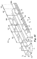
バックライト方式ディスプレイにおいて、輝度向上フィルムは、視軸に沿って光を導く構造体を使用し、それによって、視聴者に知覚される光の輝度を増強する。導光フィルムの代表的な例が図1に示されている。このフィルム10は、アクリル、ポリカーボネート、紫外線硬化アクリレート、又は類似した材料など、好適な高分子材料から製造されてよく、平滑表面14と、その平滑表面の反対側の構造化表面12とを有している。構造化表面12は、フィルムの全長に広がる複数の頂部17及び溝部18を形成するように並べて配置された線状のプリズム状要素16の配列を有している。使用の際、このフィルムの平滑表面14に比較的高い入射角で入射した光は、フィルムの平滑表面14及び構造化表面12にて屈折され、平滑表面14に対して垂直な軸線に向かって方向を変えられる。加えて、臨界角を超える角度で構造化表面12に当たる光は、プリズム状要素16の両側面、つまり切子面20から全反射を受け、後退されるが、その光は反射要素によって再利用されてもよい。反射、屈折、及び全反射の組み合わせにより、フィルム10は、軸線上に導かれる光の量を増加させ、高角度で導かれる光の量を減少させる。
In backlit displays, the brightness enhancement film uses a structure that guides light along the viewing axis, thereby enhancing the brightness of the light perceived by the viewer. A typical example of the light guide film is shown in FIG. The
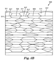
導光フィルムの第2のシートは、視軸に沿って導かれる光の量を更に増加させるために、プリズム状要素を約90度で交差させて、第1のシートに隣接して配置されてもよい。図2は、分解図にて、導光フィルムの交差したシートの向きを示している。使用の際、上方シート10’の下方の平滑表面14’は、下方シート10の構造化表面12に接触するか、あるいはほぼ接触することができる。
A second sheet of light guide film is placed adjacent to the first sheet with the prismatic elements intersecting at about 90 degrees to further increase the amount of light directed along the visual axis. Also good. FIG. 2 is an exploded view showing the direction of the intersecting sheets of the light guide films. In use, the lower
しかしながら、ディスプレイが長期間にわたって綿密に視聴される場合、非常に小さな欠陥でさえも裸眼で検出され、視聴者に混乱を生じさせることがある。例えば、「ウエットアウト」は、2つの表面が互いに光学的に接触する場合に発生し、それによって、ディスプレイの表面積全体にわたって光度の変動が生じる。輝度の高い範囲は、光結合が存在する範囲に対応し、輝度の低い範囲は、光結合が少ないことに対応しており、この変動はディスプレイが不均一な外観を有する原因となる。 However, if the display is watched closely over a long period of time, even very small defects can be detected with the naked eye, causing viewer confusion. For example, “wetout” occurs when two surfaces are in optical contact with each other, thereby causing a variation in luminous intensity across the surface area of the display. A high luminance range corresponds to a range where optical coupling exists, and a low luminance range corresponds to low optical coupling, and this variation causes the display to have a non-uniform appearance.
特に、携帯型装置において利用される小型ディスプレイに関する技術の発展により、ディスプレイの輝度を実質的に維持する一方で、ディスプレイの欠陥をより効果的に隠蔽する光学フィルムの更なる開発が必要とされている。例えば、LCDパネルの透過性が上昇していること、LCDパネル及びバックライトにおいて拡散性が低下していること、並びに、携帯型装置において間隔の許容度が小さくなり、バックライト構造が極めて薄くなっていることにより、従来のパターン付きフィルムでは、効果的に防止及び/又はマスクすることができない小規模のディスプレイ欠陥が生じることがある。 In particular, the development of technology for small displays utilized in portable devices has necessitated further development of optical films that more effectively conceal display defects while substantially maintaining display brightness. Yes. For example, the transparency of the LCD panel is increasing, the diffusivity of the LCD panel and the backlight is decreasing, and the tolerance of spacing is reduced in portable devices, making the backlight structure extremely thin. As a result, conventional patterned films can result in small display defects that cannot be effectively prevented and / or masked.
本開示において説明する導光フィルムは、マイクロ構造を上に配置したマイクロ構造化表面を有する。表面上の各マイクロ構造は、実質的に一定の高さを持つ第1の領域と、一定でない高さを持つ第2の領域とを有する。第2の領域の最大高さは第1の領域の一定の高さよりも高く、第1の領域及び第2の領域は同じ横断面形状を有する。 The light guide film described in this disclosure has a microstructured surface with a microstructure disposed thereon. Each microstructure on the surface has a first region having a substantially constant height and a second region having a non-constant height. The maximum height of the second region is higher than a certain height of the first region, and the first region and the second region have the same cross-sectional shape.
第2の領域の高さは、マイクロ構造化表面と別のディスプレイ構成要素との間の光結合を減じるように選択され、それにより、この光学フィルムを組み込んだディスプレイにおいて、広範囲に及ぶウエットアウトが防止され、視認可能な線の発生が減じられる。各マイクロ構造上の第2の領域同士の間の周期、及び/又はマイクロ構造化表面上の第2の領域の密度は、フィルムの光学ゲインを実質的に保つ一方で、この光結合の低減をもたらすように選択される。第1の領域と第2の領域は同じ横断面形状を有するので、マイクロ構造化表面は容易に複製が可能であり、それにより、これらのフィルムは、より複雑な不規則パターンを持つフィルムと比べて、製造がより安価となる。 The height of the second region is selected to reduce optical coupling between the microstructured surface and another display component, thereby providing extensive wetout in displays incorporating this optical film. And the occurrence of visible lines is reduced. The period between the second regions on each microstructure and / or the density of the second regions on the microstructured surface can substantially reduce the optical gain of the film while reducing this optical coupling. Selected to bring. Since the first region and the second region have the same cross-sectional shape, the microstructured surface can be easily replicated, so that these films are compared to films with more complex irregular patterns. Manufacturing is less expensive.
一態様において、本開示は、構造化された主表面を有する導光フィルムに関する。構造化された主表面は、第1の方向に沿って延びる複数のマイクロ構造を有する。マイクロ構造は、一定の高さを持つ第1の領域と、第1の領域に隣接する第2の領域とを有し、第2の領域は、一定でない高さ、及び第1の領域の一定の高さよりも高い最大高さを有する。第1の領域及び第2の領域は、同じ横断面形状を有する。 In one aspect, the present disclosure is directed to a light guide film having a structured main surface. The structured main surface has a plurality of microstructures extending along the first direction. The microstructure has a first region having a constant height and a second region adjacent to the first region, the second region having a non-constant height and a constant first region. The maximum height is higher than the height of The first region and the second region have the same cross-sectional shape.
別の態様において、本開示は、導光フィルムの第1のシートを有する導光物品に関する。導光フィルムの第1のシートは、構造化された主表面を有し、その構造化された主表面は、第1の方向に沿って延びる複数のマイクロ構造を有する。マイクロ構造は第1の領域と第2の領域とを有し、第2の領域は、第1の領域とは異なり、かつ第1の領域に隣接する。マイクロ構造は、第1の領域における実質的に一定の高さ、及び、第2の領域における、第1の領域の一定の高さよりも約0.5〜約3マイクロメートル高い一定でない最大高さを有する。第1の領域及び第2の領域は、同じ横断面形状を有する。 In another aspect, the present disclosure is directed to a light guide article having a first sheet of light guide film. The first sheet of the light guide film has a structured main surface, and the structured main surface has a plurality of microstructures extending along the first direction. The microstructure has a first region and a second region, and the second region is different from the first region and is adjacent to the first region. The microstructure has a substantially constant height in the first region and a non-constant maximum height in the second region that is about 0.5 to about 3 micrometers higher than the constant height of the first region. Have The first region and the second region have the same cross-sectional shape.
導光物品は、導光フィルムの第2のシートを更に有し、その導光フィルムは、実質的に平坦な表面と、その実質的に平坦な表面の反対側の構造化表面とを有する。実質的に平坦な表面は、導光フィルムの第1のシートの構造化表面に隣接する。導光フィルムの第2のシートの構造化表面は、第1の主軸に対しておおよそ垂直な第2の主軸に沿って延びる複数のマイクロ構造を有する。第1のシートと第2のシートとの間の光結合は、主として第2の領域において発生する。 The light guide article further comprises a second sheet of light guide film, the light guide film having a substantially flat surface and a structured surface opposite the substantially flat surface. The substantially flat surface is adjacent to the structured surface of the first sheet of light guide film. The structured surface of the second sheet of light guide film has a plurality of microstructures extending along a second major axis that is approximately perpendicular to the first major axis. Optical coupling between the first sheet and the second sheet occurs mainly in the second region.
更に別の態様において、本開示は、光源と、視野スクリーンと、光源から視野スクリーンに光を導く導光フィルムとを有する光学ディスプレイに関する。導光フィルムは、第1の主表面と、構造化された第2の主表面とを有し、構造化された第2の主表面は、複数のマイクロ構造を有する。マイクロ構造は、第1の領域とそれに隣接する第2の領域とを含んだ反復パターンを有する。第1の領域は一定の高さを有し、第2の領域は、第1の領域のその実質的に一定の高さよりも高い、一定でない最大高さを有する。第2の領域の最大高さは、第1の領域の一定の高さよりも約0.5μm〜約3μm高い。反復パターンは、1cm2当たり少なくとも200の第2の領域の機構密度を有し、第1の領域及び第2の領域は同じ横断面形状を有する。 In yet another aspect, the present disclosure is directed to an optical display having a light source, a viewing screen, and a light guide film that directs light from the light source to the viewing screen. The light guide film has a first main surface and a structured second main surface, and the structured second main surface has a plurality of microstructures. The microstructure has a repeating pattern including a first region and a second region adjacent to the first region. The first region has a constant height and the second region has a non-constant maximum height that is higher than the substantially constant height of the first region. The maximum height of the second region is about 0.5 μm to about 3 μm higher than the constant height of the first region. The repeating pattern has a feature density of at least 200 second regions per cm 2 , and the first region and the second region have the same cross-sectional shape.
更に別の態様において、本開示は、導光フィルムを製作する方法に関し、その方法は、構造化された主表面を備える工具を切削する工程であって、構造化された主表面が、第1の方向に沿って延びる複数の溝部を有する工程を含む。溝部は第1の領域と第2の領域とを有し、第2の領域は、第1の領域とは異なり、かつ第1の領域に隣接する。第1の領域は、実質的に一定の高さを有し、第2の領域は、第1の領域におけるその実質的に一定の高さよりも高い最大高さを有する。第1の領域及び第2の領域は、同じ横断面形状を有する。この方法は、工具に高分子材料を塗布してフィルムを形成する工程であって、フィルムが、工具の溝部に対応するマイクロ構造の配列を有する工程を更に含む。 In yet another aspect, the present disclosure relates to a method of making a light guide film, the method comprising cutting a tool with a structured major surface, wherein the structured major surface is a first. A step of having a plurality of grooves extending along the direction of. The groove has a first region and a second region, and the second region is different from the first region and is adjacent to the first region. The first region has a substantially constant height, and the second region has a maximum height that is higher than the substantially constant height in the first region. The first region and the second region have the same cross-sectional shape. The method further includes the step of applying a polymeric material to the tool to form a film, wherein the film has an array of microstructures corresponding to the grooves of the tool.
本発明の1つ以上の実施形態の詳細を、添付の図面及び以下の説明に記載する。本発明の他の特徴、目的、及び利点は、その説明と図面から、また特許請求の範囲から明らかとなろう。 The details of one or more embodiments of the invention are set forth in the accompanying drawings and the description below. Other features, objects, and advantages of the invention will be apparent from the description and drawings, and from the claims.
図3Aは、導光光学フィルム300の一実施形態の一部分を示しており、この導光光学フィルム300は、フィルムがディスプレイ装置において使用されるときに、フィルムの光学ゲインを実質的に保つ一方で、ウエットアウトを減じるかあるいは実質的に排除するように設計されたマイクロ構造の配列を有している。フィルム300は、第1の主表面302と、その反対側の構造化された主表面304とを有している。図3Aに示す実施形態において、第1の主表面302は実質的に平滑であり、これは本願において、実質的に光学的に平坦であることを意味する。しかしながら、実質的に光学的に平坦な表面302でさえも、かすみを生じる小構造体のパターンを任意に有することがある。表面302は、望ましい光学効果を達成するマイクロ構造のパターン(図3Aには示さず)を所望により有することができる。
FIG. 3A illustrates a portion of one embodiment of a light guiding
構造化表面304は、実質的に連続したパターンのマイクロ構造306を有しており、マイクロ構造306は、図3Aにおいてxで示された第1の軸方向に沿って延びており、実質的に一定の高さh1を有している。図3Aに示す実施形態において、マイクロ構造306は線状のプリズム状要素であり、各プリズム状要素は、第1の側面308と第2の側面308’とを備えている。しかしながら、図3Bに示すように、マイクロ構造306は、連続的であることを必要とせず、また、表面304は、マイクロ構造のない範囲325を有してもよい。
The
図3Aに示す実施形態を再び参照すると、側面308、308’の縁部が交差して、頂部つまり頂上342を画定している。図3Aに示す実施形態において、隣接するプリズム状要素の側面308、308’は、線状に延びる溝部344をプリズム状要素の間に形成するように交差している。しかしながら、プリズム状要素306の側面308、308’が交差することは必須ではなく、したがって、溝部344は、特定の用途に対して、必要に応じてより幅の広いものであってもよい。マイクロ構造306の平均ピッチP1は、約5μm〜約300μmまで広範囲に異なってもよいが、約15μm〜約100μmの平均ピッチが特に有用であることが判明している。ピッチP1は好ましくは、すべてのプリズム状要素306の間で実質的に同じであるが、そのような配置は必須ではなく、ピッチP1は、表面304全体にわたって一定でなくてもよい。
Referring again to the embodiment shown in FIG. 3A, the edges of the side surfaces 308, 308 ′ intersect to define a top or top 342. In the embodiment shown in FIG. 3A, the side surfaces 308, 308 ′ of adjacent prismatic elements intersect to form a linearly extending
このパターンをなす複数のマイクロ構造306の各々は、少なくとも1つの第1の領域305と、少なくとも1つの第2の領域307とを有しており、また、特定の用途に対して、必要に応じて他の領域を所望により有してもよい(他の領域は図3Aには示されていないが、例えば図6及び以下の議論を参照されたい)。各マイクロ構造306の第2の領域307は、各マイクロ構造の長さに沿って第1の領域305に隣接している。いくつかの実施形態において、第1の領域305は、2つの第2の領域307の間に設けられる。
Each of the plurality of
第1の領域305におけるマイクロ構造の横断面形状は、フィルム300の目的の用途に応じて広範に異なり得るものであり、プリズム状の形状に限定されるものではない。第1の領域305の横断面形状には、限定されるものではないが、三角形、円形、レンズ状の形状、楕円形、円錐形、又は曲線状の部分を有する非対称形状を挙げることができる。しかしながら、フィルム300の光学ゲインを最大にするためには、概ね三角形の横断面形状が好ましく、直角二等辺三角形の横断面形状が特に好ましい。第1の領域305又はマイクロ構造306の間の交差領域における横断面の三角形の頂部は、マイクロ構造又は隣接する溝部の形状を変化させ望ましい光学効果をもたらすように、平滑化されるかあるいは曲線状にされてもよいが、そのような形状は一般に、マイクロ構造によってもたらされるゲインを減じるものである。また、図3Cに示すように、マイクロ構造306Aの主軸は、望ましい光学効果を達成するように傾斜していてもよい。
The cross-sectional shape of the microstructure in the
図3Aに示す実施形態において、第1の領域305における各三角形の横断面の二面角α1は約90°であるが、70〜110°の二面角α1が、多くの用途に有用であることが判明している。
In the embodiment shown in FIG. 3A, the dihedral angle α 1 of the cross section of each triangle in the
第1の領域305は、実質的に一定の高さh1を有している。高さh1は、構造化表面304とその反対の主表面302との間にあり、かつ構造化表面304の最も近くにある平面(例えば、図3Aの基準平面320)から測定して、約1μm〜約175μmまで変動し得る。第1の領域の高さh1は実質的に同じであることが一般に好ましいが、良好な光学性能を維持しながらも、幾分かの高さの変動が許容され得る。例えば、許容可能な光学性能を維持しながらも、いくつかの実施形態において、平均高さh1は、±0.20μmだけ変動することがあり、一方で、他の実施形態において、平均高さh1は±0.10μmだけ変動することがあり、更に他の実施形態において、平均高さh1は、±0.05μmだけ変動することがある。
The
各マイクロ構造の第2の領域307が、第1の領域305に隣接している。いくつかの実施形態において、第2の領域は、第1の領域305に対して不連続であり、これは本願において、第2の領域307がマイクロ構造306上で互いに接触しないか又は重なり合わないことを意味する。第2の領域307は、目的の用途に応じて、多種多様なパターンで表面304上に配置されてよい。例えば、第2の領域307は、表面304上に不規則に分布してもよく、あるいは、その分布は半不規則的であってもよい(一部の範囲は不規則な分布、一部の範囲は規則的な分布をなし、マイクロ構造の間の最小周期などのいくつかの制限を伴う)。第2の領域307はまた、表面304上に規則的に分布してもよく、その規則的な分布は、周期的であっても(一定の間隔で繰り返す)非周期的であってもよい(不規則的でないパターンに従う)。例となる規則的な分布が図3Gのフィルム400に示されており、このフィルム400は、フィルムの表面404の全体にわたって、規則的に分布した第1の領域405と第2の領域407とを有している(第2の領域の規則的な分布の別の表現については、図12も参照されたい)。
A
第2の領域307は、構造化表面304の1cm2当たり約200〜1cm2当たり約6000の平均密度を有する。いくつかの実施形態において、第2の領域は、構造化表面304の1cm2当たり約200〜1cm2当たり約3500の平均密度を有する。他の実施形態において、第2の領域307は、構造化表面304の1cm2当たり約200〜1cm2当たり約2500の平均密度を有する。
The
第2の領域307は、約1000μm〜約20,000μmの、マイクロ構造306に沿った平均周期P2(例えば図4Aを参照されたい)を有している。いくつかの実施形態において、第2の領域307は、約3500μm〜約15,000μmの平均周期を有する。第2の領域307の平均周期P2は、好ましくは実質的に同じであるが、そのような配置は必須ではない。
図3Dにおける単一のマイクロ構造306の断面図を参照すると、第2の領域307は、第1の領域305と実質的に同じ断面形状を有しているが、単純により高いものとなっている(図3Aにおけるz方向に沿って距離h2だけ更に延びている)。例えば、図3Dに示す実施形態において、第1の領域は側面308、308’を有し、側面308、308’は、頂部342にて会合し、二面角α1を形成している。第2の領域307は側面311、311’を有し、側面311、311’は、頂部312を形成し、二面角α2を形成するように会合している。第2の領域307の二面角α2及び断面形状は、第1の領域305の二面角α1及び断面形状と実質的に同じであり、すなわちα2=α1である。また、図3Eは、第2の領域307を有するマイクロ構造化表面の一部の3つの隣接するマイクロ構造306の断面を示すものであるが、第2の領域307が、第1の領域305と実質的に同じ断面形状を有するが、距離h2だけより高いものであることを示している。
Referring to the cross-sectional view of the
断面形状におけるこの類似性は、頂部の高さにおける差異と相まって、第2の領域307の側面311、312が、俯瞰図において、マイクロ構造306(図3F)に沿って、y方向に外向きに延びているかあるいは膨張しているように見える原因となる。図3Fにおいて、第1の領域の頂部342は、実質的に直線的な線に見えるが、マイクロ構造306の間の溝部344は、第2の領域307の箇所で直線性を逸しているように見える。
This similarity in cross-sectional shape, coupled with the difference in the height of the top, causes the side surfaces 311, 312 of the
再び図3Dを参照すると、第2の領域は、第1の領域305の頂部342から第2の領域307の頂部312までで測定した、約0.5μm〜約3μmの最大高さh2を有している。いくつかの実施形態において、第2の領域の最大高さh2は約1μm〜約2.5μmであり、一方で、他の実施形態において、最大高さh2は約1.5μm〜約2μmである。第2の領域307内のすべての三角形状要素の最大高さh2は、実質的に同じであってもよいが、プリズム状要素307の高さh2は、規則的又は不規則的な方式で変動して、望ましい光学効果をもたらすことができる。
Referring again to FIG. 3D, the second region has a maximum height h 2 of about 0.5 μm to about 3 μm, measured from the top 342 of the
図4A〜4Bは、マイクロ構造306上の第2の領域307を示している。第2の領域307の高さh2が、依然として比較的一定である場合でも、第2の領域がその頂部311へと上昇してまたがる距離dは、大いに異なっていてもよい。例えば、図4Aにおいて、第2の領域を形成する線Aの傾きは、隣接する領域から滑らかに徐々に変化しており、それにより、実質的に連続する隆起状の領域がマイクロ構造306上に形成されている。図4Bにおいて、第2の領域を形成する線Bの傾きは、図4Aの線Aよりも急激に変化しており、実質的に不連続な隆起をマイクロ構造306上に形成している。
4A-4B illustrate a
使用の際、導光フィルムのシートなどの第2の表面が構造化表面304に隣接して配置されると、シート300に対するその第2の表面の物理的近接性は、マイクロ構造306の第2の領域307によって制限される。第2の領域307は、第2の表面がマイクロ構造306の第1の領域305と接触するのを防止し、それによって、光結合を減じることができる。例えば、表面304上の第2の領域307の平均密度、平均周期、及び最大高さなどの特性のいずれか又はすべて、並びに、構造化表面304を備えたフィルムを構成する材料は、フィルムの第2のシートが撓んで第1の領域305と接触することがないように選択されることができる。したがって、各マイクロ構造上の不規則に出現する第2の領域を利用して、隣接する表面の近接性を物理的に制御することにより、望ましくない光結合を受けやすい構造化表面304の表面積が飛躍的に減じられる。その代わりに、光結合は主として第2の領域307内で発生する。
In use, when a second surface, such as a sheet of light guide film, is placed adjacent to the
図5〜6は、他の有用な導光フィルムの例に関するものである。図5A〜5Bを参照すると、導光フィルム500が、マイクロ構造506を有する構造化表面504を有している。マイクロ構造506はそれぞれ、少なくとも1つの第1の領域505と、少なくとも1つの第2の領域507とを有している。各第1の領域505は、基準平面520を基準として実質的に一定の高さを有しており、各第2の領域507は、第1の領域505の実質的に一定の高さよりも高い最大高さを有している。図5A〜5Bに示す実施形態において、第2の領域507は、概ねレンズ状の形状を形成する第1及び第2の側面511、511’を有している。
5-6 relate to other examples of useful light guide films. With reference to FIGS. 5A-5B, the
図6に示す別の実施形態において、導光フィルム600が、マイクロ構造606を備えた構造化表面604を有している。マイクロ構造606はそれぞれ、少なくとも1つの第1の領域605と、少なくとも1つの第2の領域607と、少なくとも1つの第3の領域609とを有している。各第1の領域605は、基準平面620を基準として実質的に一定の高さを有しており、各第2の領域607は、第1の領域605の実質的に一定の高さよりも高い最大高さを有している。各第3の領域609は、第1の領域605の実質的に一定の高さよりも高いが、第2の領域607の最大高さ未満である最大高さを有している。そのような構成は、例えば、隣接するフィルムが、第2の領域607同士の間の範囲において撓むときに生じる光結合を減じるのに有用となり得る。図6に示す実施形態において、第2及び第3の領域は、実質的に不連続である(図4Bの概略図を参照されたい)。図3Aのマイクロ構造の第1の領域305と第2の領域307との境界面における比較的平滑な曲線は、本明細書において連続的と称されるが(図4Aの概略図も参照されたい)、この比較的平滑な曲線と比較すると、図6における側面611、611’及び613、613’と側面608、608’との境界面は非常に険しいものであり、この境界面は本明細書において不連続な構造と称される。
In another embodiment shown in FIG. 6, the
図7〜9は、本明細書で説明する導光フィルムの更なる例示的実施形態を示す顕微鏡写真である。図7〜9は、構造化表面704を備えた導光フィルム700の一部分の、倍率を増加させた3つの図を示しており、この構造化表面704は、x方向に沿って延びる連続的なプリズム状のマイクロ構造706を有している。マイクロ構造706は、暗い縞又はより暗い部分として現れる第1の領域705、並びに、より明るい着色した縞として現れる、不規則に分布した第2の領域707を有している。第2の領域707は、第1の領域705の実質的に一定の高さよりも高い、z方向に沿った最大高さを有している。第2の領域707はまた、その三角形状の断面輪郭が第1の領域705の断面輪郭と依然として同じとなるように、y方向に沿って外向きに延びている。図10〜11は、図7〜9に示す導光フィルム700の実施形態の、倍率を増加させた更なる俯瞰図である。図3Fと同様に、第1の領域の頂部742は、実質的に直線的な線に見えるが、マイクロ構造706の間の溝部744は、第2の領域707の箇所で直線性を逸しているように見える。
7-9 are photomicrographs illustrating further exemplary embodiments of the light guide films described herein. FIGS. 7-9 show three increased magnification views of a portion of a
図12は、構造化表面804を備えた導光フィルム800の一部分を示しており、この構造化表面804は、x方向に沿って延びる連続的なプリズム状のマイクロ構造806を有している。これらのマイクロ構造は、第1の領域805、並びに、実質的に規則的に分布した第2の領域807を有しており、第2の領域807は、隆起した部分としてマイクロ構造806の1つおきに現れている。第2の領域807は、第1の領域805の実質的に一定の高さよりも高い、z方向に沿った最大高さを有している。第2の領域807はまた、その三角形状の断面輪郭が第1の領域805の断面輪郭と依然として同じとなるように、y方向に沿って外向きに延びている。
FIG. 12 shows a portion of a
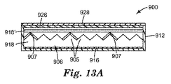
図13Aは、本明細書で説明する導光フィルムを組み込んだディスプレイ900の代表的な実施形態を、断面図で示している。ディスプレイ900は、ケース912と、光源916と、導光フィルム918の第1のシートと、導光フィルム918’の第2のシートと、光ゲート装置926と、実質的に透明なカバーシート928とを有している。図13Aにて開示する実施形態において、光源916は、例えば、LED、有機LED、エレクトロルミネセントパネル、又は蛍光光源とされることができる。加えて、図13Aにて開示する光ゲート装置926は、好ましくは液晶装置であるが、他の光ゲート装置が使用されてもよい。
FIG. 13A illustrates, in cross-section, an exemplary embodiment of a
導光フィルム918の第1のシートは、図3Aに示す実施形態を例示するものであり、第1の領域905と第2の領域907とを備えたマイクロ構造906を有している。マイクロ構造906は、第1及び第2の領域905、907の各々において同じ断面形状を有している。第1の領域905は、実質的に一定の高さを有し、第2の領域907は、第1の領域905のその実質的に一定の高さよりも高い最大高さを有している。図13Aが一定の縮尺で描かれていないこと、並びに、特に、導光フィルム918の構造化表面の寸法が、説明の目的で大いに誇張されていることは理解されよう。図13Aに示すように、第2の領域907の頂点は、第1のシート918に対する導光フィルム918’の第2のシートの物理的近接性を制御する。先の議論によれば、光結合は、比較的高い頂点を有する箇所に集中しており、それらの頂点は好ましくは、高さが約1μm乃至約2.5μmである。図13Aは、マイクロ構造の頂点907が光源916に背くような方向に向き付けられた導光フィルムを示しているが、別の実施形態において、頂点507は光源916に向けられてもよい。
The first sheet of the
図13Bは、本明細書で説明する導光フィルムのシートの別の有用な応用例を示している。図13Bは、光学ディスプレイにおいて使用するための、一般に使用されている光ガイドアセンブリ950の概略図である。光ガイドアセンブリ950は、光源952と、楔形状の光ガイド954と、拡散反射体956と、導光フィルム958のシートとを有している。使用の際、光源952からの光は、光ガイド954の中に導かれる。光ガイド954の表面に臨界角を超える角度で当たる光線は、全反射を受け、光ガイド954に沿って伝搬される。対照的に、光ガイド954の表面に臨界角未満の角度で当たる光線は、透過及び屈折される。光ガイド954の底面を抜け出した光線は、拡散反射体956によって反射され、「再循環」されて使用される。光ガイド954の頂面を抜け出した光線は、液晶装置などの光ゲート手段を通過して、ディスプレイ上に画像を生成する。
FIG. 13B illustrates another useful application of a sheet of light guide film as described herein. FIG. 13B is a schematic diagram of a commonly used
図1に示すような従来の導光フィルムは、導光フィルムの構造化表面955と光ガイド954の上側表面953との間に光結合を発生させることがある。導光フィルム958の構造化表面955上のマイクロ構造957は、光ガイド954に対する導光フィルム958の構造化表面955の近接性を制御することによって視認可能な光結合の発生を抑制する第2の領域960を有している。
A conventional light guide film as shown in FIG. 1 may cause optical coupling between the
導光フィルムに使用される特定の材料は、目的の用途に応じて広範に異なり得るが、その材料は、高度な光の透過性を確保するために、実質的に透明であるべきである。この目的に有用な高分子材料が市販されており、例えば、それぞれ約1.493及び1.586の公称屈折率を有するアクリル及びポリカーボネートが挙げられる。他の有用なポリマーには、ポリプロピレン、ポリウレタン、ポリスチレン、ポリ塩化ビニルなどが挙げられる。高い屈折率を有する材料が一般に好ましい。 The particular material used for the light guide film can vary widely depending on the intended application, but the material should be substantially transparent to ensure a high degree of light transmission. Useful polymeric materials for this purpose are commercially available and include, for example, acrylics and polycarbonates having nominal refractive indices of about 1.493 and 1.586, respectively. Other useful polymers include polypropylene, polyurethane, polystyrene, polyvinyl chloride, and the like. A material having a high refractive index is generally preferred.
導光フィルムの基材として使用され得る平滑なポリエステルフィルムが、ヴァージニア州ホープウェル(Hopewell)のICIアメリカズ社(ICI Americas Inc.)からMelinex 617の商標標記で市販されている。基材として使用されるフィルムに塗布され得る艶消し仕上げコーティングが、ウィスコンシン州ニューバーリン(New Berlin)のテクラ社(Tekra Corporation)からMarnot 75 GUの商標標記で市販されている。他のフィルムが同様に使用されてもよい。これらのフィルムは、光学特性、機械的特性、及び他の特性により選択されてもよい。例えば、基材は、公開済みのPCT特許出願第97/01774号に記載されているような多層光学フィルムであってもよい。使用され得る他のフィルムの例が、波長選択型の多層光学フィルム及び反射偏光子である。反射偏光子は、多層フィルム、コレステリック物質、又は公開済みのPCT特許出願第97/32227号に開示されている種類の物質であってもよい。 A smooth polyester film that can be used as a substrate for a light guide film is commercially available from ICI Americas Inc., Hopewell, Va., Under the trademark Melinex 617. A matte finish coating that can be applied to films used as substrates is commercially available from Tekra Corporation, New Berlin, Wisconsin, under the Marnot 75 GU trademark designation. Other films may be used as well. These films may be selected according to optical properties, mechanical properties, and other properties. For example, the substrate may be a multilayer optical film as described in published PCT patent application 97/01774. Examples of other films that can be used are wavelength selective multilayer optical films and reflective polarizers. The reflective polarizer may be a multilayer film, a cholesteric material, or a material of the type disclosed in published PCT Patent Application No. 97/32227.
本明細書で説明する導光フィルムを製造するために使用される工具のマスターは、押出しによるかあるいはキャスト及び硬化プロセスによるかにかかわらず、既知のダイヤモンド旋盤技術で製作されてよい。好適なダイヤモンド旋盤機が、米国特許第6,322,236号、同第6,354,709号、同第7,328,638号、及び国際公開第00/48037号において図示され、説明されている。 The master of the tool used to produce the light guide film described herein may be made with known diamond lathe technology, whether by extrusion or by casting and curing processes. Suitable diamond lathes are illustrated and described in US Pat. Nos. 6,322,236, 6,354,709, 7,328,638, and WO 00/48037. Yes.
これらの方法で使用される、導光フィルムを製作するための機器には、一般に、高速工具サーボ(fast servo tool)が挙げられる。高速工具サーボ(FTS)は、PZTスタックと呼ばれる固体圧電(PZT)装置であり、このPZTスタックは、PZTスタックに取り付けられた切削工具の位置を迅速に調節するものである。このFTSにより、以下で更に説明する座標系内の各方向に、切削工具を非常に正確にかつ高速に移動させることが可能となる。 The equipment for producing the light guide film used in these methods generally includes a fast servo tool. The fast tool servo (FTS) is a solid state piezoelectric (PZT) device called a PZT stack, which quickly adjusts the position of a cutting tool attached to the PZT stack. This FTS makes it possible to move the cutting tool very accurately and at high speed in each direction in a coordinate system that will be further described below.
図14は、ワークピースにマイクロ構造を製作するための切削工具システム1000の略図である。マイクロ構造は、任意の種類、形状、及び寸法の、物品の表面上にある構造体、物品の表面の中に刻まれた刻み目、又は物品の表面から突き出る突出部を有することができる。システム1000はコンピュータ1012によって制御される。コンピュータ1012は、例えば以下の構成要素を、つまり、1つ以上のアプリケーション1016を記憶するメモリー1014と、情報を不揮発性で記憶する第2の記憶装置1018と、情報又はコマンドを受信するための入力装置1020と、メモリー1016若しくは第2の記憶装置1018に記憶された、又は別の供給源から受け取られたアプリケーションを実行するためのプロセッサ1022と、情報の視覚表示を出力するためのディスプレイ装置1024と、音声情報用のスピーカー又は情報のハードコピー用のプリンターなど、情報を他の形式で出力するための出力装置1026とを有する。
FIG. 14 is a schematic diagram of a
ワークピース1054の切削は、工具先端部1044によって実施される。アクチュエータ1038は、ワークピース1054が、コンピュータ1012によって制御される電気モーターなど、駆動ユニット及びエンコーダ1056によって回転される際に、工具先端部1044の移動を制御する。この実施例において、ワークピース1054はロールの形態で示されているが、平面的な形態で実現されることもできる。任意の機械加工可能な材料が使用されてよく、例えば、ワークピースは、アルミニウム、ニッケル、銅、真鍮、鋼、又はプラスチック(例えばアクリル)で実現されることができる。使用される特定の材料は、例えば、機械加工されたワークピースを使用して製作される各種フィルムなど、特定の望ましい用途に依存してもよい。アクチュエータ1038は、例えば、ステンレス鋼で、あるいは他の材料で実現されることができ、好適なアクチュエータが、例えば、米国特許第7,328,638号において図示され、説明されている。
The
アクチュエータ1038は、工具台1036に取り外し可能に連結されており、工具台1036はトラック1032上に位置している。工具台1036及びアクチュエータ1038は、矢印1040及び1042で示すx方向及びz方向の双方に移動するように、トラック1032上に構成されている。コンピュータ1012は、1つ以上の増幅器1030を介して工具台1036及びアクチュエータ1038と電気的に接続されている。
The
制御器として機能する場合、コンピュータ1012は、ワークピース1054を機械加工するために、トラック1032に沿った工具台1036の移動、及び工具先端部1044の移動を、アクチュエータ1038によって制御する。アクチュエータが複数のPZTスタックを有する場合、そのアクチュエータは、スタックに取り付けられた工具先端部の移動を独立に制御する上で使用するために、別々の増幅器を使用して各PZTスタックを独立に制御することができる。以下で更に説明するように、コンピュータ1012は、様々なマイクロ構造をワークピース1054に機械加工するために、関数発生器1028を利用して波形をアクチュエータ1038に供給することができる。
When functioning as a controller, the
ワークピース1054の機械加工は、様々な構成要素の移動を調整することによって達成される。具体的に言えば、システムは、コンピュータ1012の制御下で、工具台1036の移動を通じてアクチュエータ1038の移動を、c方向(図14の線1053で表す回転移動)におけるワークピースの移動、並びにx方向、y方向、及びz方向のうちの1つ以上における工具先端部1044の移動と共に調整及び制御することができる。これらの座標については以下で説明する。システムは通常、一定の速度でz方向に工具台1036を移動させるが、変動する速度が用いられてもよい。工具台1036及び工具先端部1044の移動は通常、c方向におけるワークピース1054の移動と同期される。これらの移動のすべては、例えば、数値制御技術、又は、ソフトウェア、ファームウェア、若しくはそれらの組み合わせでコンピュータ1012に実装された数値制御器(NC)を用いて制御されることができる。
Machining of
ワークピースの切削は、連続的及び不連続的な切削運動を含むことができる。ロールの形態をなすワークピースの場合、その切削には、螺旋型の切削(時にねじ切りとも呼ばれる)、又は、ロールの周り若しくはロールの付近の個々の輪としての切削が挙げられる。平面の形態をなすワークピースの場合、その切削には、渦巻き型の切削、又は、ワークピース上若しくはワークピースの付近の個々の輪としての切削が挙げられる。またX切削が用いられることができ、このX切削は、ほぼ直線的な切断形式を伴うものであり、ダイヤモンドの工具先端部は、横に移動してワークピースに出入りすることができるが、工具台の全体的な動作は直線的である。切削はまた、これらの種類の運動の組み合わせを含むこともできる。 Cutting the workpiece can include continuous and discontinuous cutting motions. In the case of a workpiece in the form of a roll, the cutting may include helical cutting (sometimes referred to as threading) or cutting as individual rings around or in the vicinity of the roll. In the case of a workpiece in the form of a plane, the cutting may include spiral cutting or cutting as individual rings on or near the workpiece. X cutting can also be used, and this X cutting is accompanied by a substantially linear cutting form, and the diamond tool tip can move sideways to enter and exit the workpiece. The overall movement of the table is linear. Cutting can also include a combination of these types of motion.
ワークピース1054は、機械加工された後、多様な用途での使用に対応するマイクロ構造を有するフィルムを製作するために使用されることができる。フィルムは通常、コーティングプロセスを用いて製作され、そのコーティングプロセスにおいて、粘性の状態にある高分子材料がワークピースに塗布され、少なくとも部分的に硬化され、次いで取り外される。硬化した高分子材料で構成されたフィルムは、実質的に、ワークピースの構造体と正反対の構造体を有することになる。例えば、ワークピース内のくぼみは、結果として得られるフィルムに突出部をもたらす。ワークピース1054はまた、機械加工された後、工具の要素又はマイクロ構造と対応する独立した要素又はマイクロ構造を有する他の物品を製作するために使用されることもできる。
Once the
工具台1036及びアクチュエータ1038の温度をライン1048及び1050を通じて制御するために、冷却液1046が使用されている。温度制御ユニット1052は、冷却液が工具台1036及びアクチュエータ1038を通じて循環されるとき、冷却液の温度を実質的に一定に維持することができる。温度制御ユニット1052は、流体の温度を制御する任意の装置で実現されることができる。冷却液は、油製品、例えば低粘度油で実現されることができる。温度制御ユニット1052及び冷却液1046の貯蔵部は、工具台1036及びアクチュエータ1038を通じて流体を循環させるポンプを有することができ、また、通常、流体を実質的に一定の温度に維持するために、流体から熱を除去する冷房システムを有している。特定の実施形態において、冷却液はまた、ワークピースにおいて機械加工される材料の表面温度を実質的に一定に維持するために、ワークピース54に作用されることもできる。
図15は、システム10などの切削工具の座標系を示す略図である。この座標系は、ワークピース1064を基準とした工具先端部1062の移動として示されている。工具先端部1062は、工具先端部1044と対応してもよく、通常、キャリア1060に取り付けられ、キャリア1060はアクチュエータに取り付けられる。座標系は、この例示的実施形態において、x方向1066と、y方向1068と、z方向1070とを含んでいる。x方向1066は、ワークピース1064に対して実質的に垂直な方向における移動に関するものである。y方向1068は、ワークピース1064の回転面に対して実質的に平行な方向など、ワークピース1064を横切る方向における移動に関するものである。z方向1070は、ワークピース1064の回転軸線に対して実質的に平行な方向など、長手方向にワークピース1064に沿う方向における移動に関するものである。ワークピースの回転は、図14にも示すように、c方向と呼ばれる。ワークピースが、ロールの形態ではなく平面の形態で実現される場合、y方向及びz方向は、x方向に対して実質的に垂直な方向でワークピース全体にわたる、相互に直交する方向における移動に関するものとなる。平面的な形態のワークピースには、例えば、回転円板、又は他の任意の外形の平面的な材料を挙げることができる。
FIG. 15 is a schematic diagram illustrating the coordinate system of a cutting tool such as
図16Aは、本開示で説明した導光フィルムを製作する上で使用され得る典型的な工具先端部1062の斜視図であり、図16Bはその正面図であり、図16Cはその底面図であり、図16Dはその側面図である。図16A〜16Dに示すように、工具先端部1062は、側面1104と、テーパが付けられ角度が付けられた正面1106と、先端部1062を好適な工具先端部キャリア(図16A〜16Dには示さず)に固定するための底面1102とを有している。工具先端部1062の正面部分1105は、アクチュエータの制御下でワークピースを機械加工するために使用される。工具先端部1062は、例えば、ダイヤモンドの厚板(diamond slab)で実現されてもよい。
16A is a perspective view of an exemplary tool tip 1062 that can be used in making the light guide film described in this disclosure, FIG. 16B is a front view thereof, and FIG. 16C is a bottom view thereof. FIG. 16D is a side view thereof. As shown in FIGS. 16A-16D, the tool tip 1062 includes a
一実施形態において、ダイヤモンド旋盤への1回の送り込みでマイクロ構造上に第1及び第2の領域を生成するために、高速工具サーボアクチュエータが、ダイヤモンド旋盤機に加えられる。別の実施形態において、導光フィルム上のマイクロ構造の第1の領域は、ダイヤモンド旋盤への初回の送り込みで生成されてもよく、工具は、実質的に一定の深さでロールに切り込むように設定される。次いで、ダイヤモンド旋盤への2回目の送り込みで、同じ工具が使用されて、マイクロ構造の第2の領域が、規則的、不規則的、又は疑似不規則的なパターンで切削される。 In one embodiment, a high speed tool servo actuator is added to the diamond lathe machine to create the first and second regions on the microstructure with a single feed to the diamond lathe. In another embodiment, the first region of the microstructure on the light guide film may be created with an initial feed into the diamond lathe so that the tool cuts into the roll at a substantially constant depth. Is set. Then, on the second feed to the diamond lathe, the same tool is used to cut the second region of the microstructure in a regular, irregular or pseudo irregular pattern.
1回の送り込みによる切削プロセスか又は複数回の送り込みによる切削プロセスかの選択は、マイクロ構造上の第2の領域の形状に影響を与えることがある。例えば、1回の送り込みによる切削プロセスでは、実質的に連続する第2の領域を有するマイクロ構造が生成され、第2の領域は、平滑でより緩慢に変化する傾きを持つ(図4A)。通常、複数回の送り込みによる切削プロセスでは、険しい不連続な形状を持つ第2の領域が生成され、その形状は、急激に変化する傾きを有するものである(図4B)。 The choice of a single feed or multiple feed cutting process can affect the shape of the second region on the microstructure. For example, a single infeed cutting process produces a microstructure with a second region that is substantially continuous, with the second region having a smooth and more slowly varying slope (FIG. 4A). Usually, in the cutting process by a plurality of times of feeding, a second region having a steep discontinuous shape is generated, and the shape has a slope that changes abruptly (FIG. 4B).
ここで、本発明について、以下の非限定的な実施例を参照して更に説明することにする。 The invention will now be further described with reference to the following non-limiting examples.
ダイヤモンド旋盤プロセスを用いて表面を調製したロールから、第1及び第2の領域を備えたマイクロ構造を有する導光フィルムを製作した。そのロールは、パターン付きの溝部を有するものであったが、その溝部は、例えば、米国特許第6,322,709号及び同第7,328,638号に記載されているような高速工具サーボアクチュエータを使用して、1回の送り込みで生成されたものであった。次いで、高分子材料をロールの上に流して、溝部となったダイヤモンド切削パターンを複写するマイクロ構造化表面を備えるフィルムを形成した。フィルムのパターンの特徴を以下の表1に示す。 A light guide film having a microstructure with first and second regions was fabricated from a roll whose surface was prepared using a diamond lathe process. The roll had a patterned groove, which was a high speed tool servo as described, for example, in US Pat. Nos. 6,322,709 and 7,328,638. It was generated with a single feed using an actuator. The polymeric material was then flowed over a roll to form a film with a microstructured surface that replicated the diamond cutting pattern that became the groove. The characteristics of the film pattern are shown in Table 1 below.
表1において、最大周期及び平均周期は、マイクロ構造に沿って評価されている。マイクロ構造に沿った周期は、ある第2の領域の始点から、同じマイクロ構造上の隣接する第2の領域の始点にわたって測定されている。 In Table 1, the maximum period and the average period are evaluated along the microstructure. The period along the microstructure is measured from the start of one second region to the start of an adjacent second region on the same microstructure.
表1におけるウエットアウトの格付けを決定するために、各サンプルのマイクロ構造化した側面を、図1に示すマイクロ構造フィルムなどの別のマイクロ構造化フィルムの平滑な側面の隣に置いた。サンプルを、図2に示すように向き付けした。ライトテーブル上で観察した際に、フィルム間の光結合の量を主観的に評価し、以下の格付け方式を用いて格付けした。 To determine the wet-out rating in Table 1, the microstructured side of each sample was placed next to the smooth side of another microstructured film, such as the microstructured film shown in FIG. The sample was oriented as shown in FIG. When observed on a light table, the amount of optical coupling between films was subjectively evaluated and rated using the following rating system.
0−ウエットアウト見られず
1−ウエットアウトは非常に軽度であり、確認はやや困難である
2−ウエットアウトは目立たないが、依然として視認可能である
3−ウエットアウトは容易に視認可能である
4−ウエットアウトは明るいが、線のパターンはない
5−明るいウエットアウトであり、線のパターンを伴う
表1における審美的な格付けを決定するために、1枚のフィルムサンプルをライトテーブル上に置き、その外観を、ミネソタ州セントポール(St. Paul)のスリーエム社(3M Company)からBEF 2及びBEF 3の商標標記で入手可能な従来の導光フィルムの外観と比べて、主観的に評価した。1の評価をBEF 2に与え、5の評価をBEF 3に与えた。
0-Wet-out not seen 1-Wet-out is very mild and is a little difficult to confirm 2- Wet-out is inconspicuous but still visible 3- Wet-out is easily visible 4 -Wetout bright but no line pattern 5-Bright wetout with line pattern To determine the aesthetic rating in Table 1 a film sample is placed on a light table, Its appearance was evaluated subjectively compared to the appearance of conventional light guide films available under the
表1におけるゲインの変化を決定するために、実質的に一定の高さを持つ線状のプリズム状構造を有し、かつ第2の領域を持たない導光フィルム(例えば、図1の導光フィルムを参照されたい)とサンプルを比較した。 In order to determine the gain change in Table 1, a light guide film having a linear prismatic structure with a substantially constant height and no second region (eg, the light guide of FIG. 1). Samples were compared to (see film).

表1に示す結果に加えて、フィルムの性能を図17〜18にまとめる。 In addition to the results shown in Table 1, the film performance is summarized in FIGS.
図17は、フィルム上の第2の領域の密度に対して第2の領域の高さをプロットすることによって、表1のフィルムの耐ウエットアウト性能をまとめたものである。一般に、図17にプロットした結果が示すところによれば、約1〜約2マイクロメートルの高さと、1cm2当たり約200〜約3500の第2の領域の平均の機構密度を有する第2の領域により、最良の耐ウエットアウト性能がもたらされる。 FIG. 17 summarizes the wet-out performance of the films in Table 1 by plotting the height of the second region against the density of the second region on the film. In general, the results plotted in FIG. 17 indicate that a second region having a height of about 1 to about 2 micrometers and an average feature density of the second region of about 200 to about 3500 per cm 2. Provides the best wet out performance.
図18は、第2の領域の平均周期に対して第2の領域の高さをプロットすることによって、表1のフィルムの耐ウエットアウト性能をまとめたものである。一般に、図18にプロットした結果が示すところによれば、約1〜約2マイクロメートルの高さと、約1000μm〜約12000μmの平均の機構周期を有する第2の領域により、最良の耐ウエットアウト性能がもたらされる。 FIG. 18 summarizes the wet-out performance of the films in Table 1 by plotting the height of the second region against the average period of the second region. In general, the results plotted in FIG. 18 show that the best wet-out performance with a second region having a height of about 1 to about 2 micrometers and an average mechanical period of about 1000 μm to about 12000 μm. Is brought about.
上記のように、本発明は、ディスプレイシステムに応用可能であり、バックライト方式ディスプレイ及び背面映写スクリーンなど、複数の光管理フィルムを有するディスプレイ及びスクリーンにおける審美的欠陥を減じる上で特に有用であると考えられる。したがって、本発明は、上述の特定の実施例に限定されるとみなされるべきではなく、むしろ、添付の特許請求の範囲において明確に記載された本発明のすべての態様を網羅すると理解されるべきである。様々な修正、等価なプロセス、並びに本発明の適用が可能となり得る多数の構造体が、本発明の対象とされる当業者には、本明細書を検討すれば容易に明らかとなろう。特許請求の範囲は、そのような修正及び工夫を網羅することを意図したものである。 As noted above, the present invention is applicable to display systems and is particularly useful in reducing aesthetic defects in displays and screens having multiple light management films, such as backlighted displays and rear projection screens. Conceivable. Accordingly, the invention is not to be seen as limited to the specific embodiments described above, but rather is to be construed as covering all aspects of the invention explicitly set forth in the appended claims. It is. Various modifications, equivalent processes, as well as numerous structures that may be applicable to the present invention will be readily apparent to those of skill in the art to which the present invention is directed upon review of this specification. The claims are intended to cover such modifications and devices.
Claims (3)
一定の高さと、第1の二面角α 1 を有する第1の頂部と、を有する第1の領域と、
前記第1の領域に隣接する第2の領域であって、一定でない高さと、前記第1の領域の前記一定の高さよりも高い最大高さと、α 1 と同じ第2の二面角α 2 を有する第2の頂部と、を有し、前記第1の領域と前記第2の領域とは同じ横断面形状を有する、第2の領域と、
を備える、導光フィルム。 A light guide film comprising a structured main surface, wherein the structured main surface comprises a plurality of microstructures extending along a first direction,
A first region having a constant height and a first apex having a first dihedral angle α 1 ;
A second area adjacent to the first region, the height is not constant, wherein the constant maximum and height greater than the height, alpha 1 identical second dihedral angle of the first region and a second top having alpha 2, and have the same cross-sectional shape between the first region and the second region, the second region,
A light guide film.
Applications Claiming Priority (3)
| Application Number | Priority Date | Filing Date | Title |
|---|---|---|---|
| US4175108P | 2008-04-02 | 2008-04-02 | |
| US61/041,751 | 2008-04-02 | ||
| PCT/US2009/039077 WO2009124107A1 (en) | 2008-04-02 | 2009-04-01 | Light directing film and method for making the same |
Related Child Applications (1)
| Application Number | Title | Priority Date | Filing Date |
|---|---|---|---|
| JP2014096266A Division JP5873130B2 (en) | 2008-04-02 | 2014-05-07 | Light guide film and method for producing light guide film |
Publications (3)
| Publication Number | Publication Date |
|---|---|
| JP2011517035A JP2011517035A (en) | 2011-05-26 |
| JP2011517035A5 JP2011517035A5 (en) | 2012-05-24 |
| JP5827120B2 true JP5827120B2 (en) | 2015-12-02 |
Family
ID=41135927
Family Applications (2)
| Application Number | Title | Priority Date | Filing Date |
|---|---|---|---|
| JP2011503130A Active JP5827120B2 (en) | 2008-04-02 | 2009-04-01 | Light guide film and method for producing light guide film |
| JP2014096266A Active JP5873130B2 (en) | 2008-04-02 | 2014-05-07 | Light guide film and method for producing light guide film |
Family Applications After (1)
| Application Number | Title | Priority Date | Filing Date |
|---|---|---|---|
| JP2014096266A Active JP5873130B2 (en) | 2008-04-02 | 2014-05-07 | Light guide film and method for producing light guide film |
Country Status (6)
| Country | Link |
|---|---|
| US (2) | US9810817B2 (en) |
| JP (2) | JP5827120B2 (en) |
| KR (1) | KR101609400B1 (en) |
| CN (2) | CN101981474A (en) |
| TW (1) | TWI483013B (en) |
| WO (1) | WO2009124107A1 (en) |
Families Citing this family (24)
| Publication number | Priority date | Publication date | Assignee | Title |
|---|---|---|---|---|
| JPS6358322A (en) * | 1986-08-29 | 1988-03-14 | Canon Inc | Control system for light transmissivity |
| CN102016656A (en) * | 2008-04-02 | 2011-04-13 | 3M创新有限公司 | Methods and systems for fabricating optical films having superimposed features |
| KR101609400B1 (en) * | 2008-04-02 | 2016-04-05 | 쓰리엠 이노베이티브 프로퍼티즈 컴파니 | Light directing film or light directing article |
| JP2011209414A (en) * | 2010-03-29 | 2011-10-20 | Dainippon Printing Co Ltd | Optical sheet, optical element, surface light source device, transmission type display device, and light-emitting device |
| US8427747B2 (en) * | 2010-04-22 | 2013-04-23 | 3M Innovative Properties Company | OLED light extraction films laminated onto glass substrates |
| JP2012018330A (en) * | 2010-07-09 | 2012-01-26 | Dainippon Printing Co Ltd | Optical sheet |
| JP6006207B2 (en) * | 2010-08-02 | 2016-10-12 | スリーエム イノベイティブ プロパティズ カンパニー | Uniform photo-alignment film and method for producing the same |
| JP5789931B2 (en) * | 2010-08-25 | 2015-10-07 | 大日本印刷株式会社 | Prism sheet, surface light source device and liquid crystal display device |
| GB201020718D0 (en) * | 2010-12-07 | 2011-01-19 | Microsharp Corp Ltd | Structured optical film |
| KR20120078503A (en) * | 2010-12-31 | 2012-07-10 | 코오롱인더스트리 주식회사 | Optical sheet |
| WO2012114267A1 (en) * | 2011-02-22 | 2012-08-30 | Koninklijke Philips Electronics N.V. | Collimator comprising a prismatic layer stack, and lighting unit comprising such a collimator |
| CN102289025B (en) * | 2011-07-20 | 2013-07-24 | 深圳市华星光电技术有限公司 | Light guide plate and back light module |
| US8821002B2 (en) | 2011-07-20 | 2014-09-02 | Shenzhen China Star Optoelectronics Technology Co., Ltd. | Light guide plate and backlight module |
| US9004726B2 (en) | 2011-10-27 | 2015-04-14 | Svv Technology Innovations, Inc. | Light directing films |
| WO2013116104A1 (en) | 2012-01-31 | 2013-08-08 | 3M Innovative Properties Company | Light directing films and methods of making same |
| US9046225B2 (en) * | 2013-08-16 | 2015-06-02 | General Electric Company | Lighting system with improved illumination distribution |
| TWI515490B (en) * | 2013-09-25 | 2016-01-01 | 友達光電股份有限公司 | Display device |
| JP2017527948A (en) | 2014-06-26 | 2017-09-21 | フィリップス ライティング ホールディング ビー ヴィ | Small LED lighting unit |
| CN106226849B (en) * | 2014-08-26 | 2019-03-01 | 友辉光电股份有限公司 | The method for forming the method for concaveconvex structure on substrate and forming optical film |
| CN106226859B (en) * | 2015-06-02 | 2019-09-06 | 友辉光电股份有限公司 | Light directing film |
| US10359557B2 (en) | 2017-05-03 | 2019-07-23 | Wuhan China Star Optoelectronics Technology Co., Ltd. | Light guide plate having periodic microstructure configured on light emission surface and a light waveguide layer configured within transmission layer and backlight module having a collimation structure configured with a plurality of collimation-layer units and a plurality of collimation-optical-lens units to collimate light beams emitted from the light emission surface of the light guide plate |
| CN107102396B (en) * | 2017-05-03 | 2019-06-11 | 武汉华星光电技术有限公司 | A kind of light guide plate and the backlight module using the light guide plate |
| KR102618812B1 (en) * | 2018-10-31 | 2023-12-28 | 삼성디스플레이 주식회사 | Foldable display device |
| CN112462456B (en) * | 2020-11-29 | 2023-10-20 | 昇印光电(昆山)股份有限公司 | Optical film, manufacturing method and electronic equipment cover plate carrying same |
Family Cites Families (179)
| Publication number | Priority date | Publication date | Assignee | Title |
|---|---|---|---|---|
| US2733730A (en) | 1956-02-07 | turak | ||
| US1348115A (en) | 1918-08-31 | 1920-07-27 | Leon G Buckwalter | Reversible-taper roughing-reamer |
| US2404222A (en) | 1944-05-23 | 1946-07-16 | Ralph D Doner | Diffraction grating tool |
| FR967169A (en) | 1948-05-18 | 1950-10-27 | One-piece phonograph needle or style, but two-piece of different flexibility and stiffness | |
| DE885163C (en) | 1951-06-16 | 1953-08-03 | Blaupunkt Elektronik G M B H | Universal double needles for normal and micro-groove records |
| US2738730A (en) | 1952-07-01 | 1956-03-20 | Fairchild Camera Instr Co | Method for forming engraved image-reproducing plates |
| CH359899A (en) | 1959-07-24 | 1962-01-31 | Colomb Andre | A method of manufacturing a sapphire needle for a speaking machine and a needle obtained by implementing this method |
| US3293727A (en) | 1961-04-12 | 1966-12-27 | Bilt Rite Tool & Machine Co | Cutting tool |
| US3417959A (en) | 1966-11-14 | 1968-12-24 | Minnesota Mining & Mfg | Die for forming retro-reflective article |
| US3680213A (en) | 1969-02-03 | 1972-08-01 | Karl O Reichert | Method of grooving semiconductor wafer for the dividing thereof |
| US3780409A (en) | 1971-02-19 | 1973-12-25 | Fansteel Inc | Threading tool |
| US3813970A (en) | 1972-01-10 | 1974-06-04 | Ammco Tools Inc | Tool holder |
| US4012843A (en) | 1973-04-25 | 1977-03-22 | Hitachi, Ltd. | Concave diffraction grating and a manufacturing method thereof |
| US3893356A (en) | 1974-03-19 | 1975-07-08 | Frank Atzberger | Rotor cutter |
| US4035590A (en) | 1975-06-30 | 1977-07-12 | Rca Corporation | Apparatus for electromechanical recording of short wavelength modulation in a metal master |
| US4044379A (en) | 1975-06-30 | 1977-08-23 | Rca Corporation | Method and apparatus for electromechanical recording of short wavelength modulation in a metal master |
| US4113267A (en) | 1977-04-25 | 1978-09-12 | Pickering & Company, Inc. | Double stylus assembly for phonograph record stamper playback |
| US4113266A (en) | 1977-04-25 | 1978-09-12 | Pickering & Company, Inc. | Playback stylus for phonograph record stamper |
| US4111083A (en) | 1977-08-08 | 1978-09-05 | Carter Walter L | Tool holder |
| US4287689A (en) | 1979-10-30 | 1981-09-08 | Rca Corporation | Method for improving the quality of low frequency output of a video disc pickup stylus |
| US4417489A (en) | 1979-12-21 | 1983-11-29 | Liu Chunghorng R | Method and apparatus for machining a workpiece by varying the tool geometry |
| US4355382A (en) | 1980-12-24 | 1982-10-19 | Rca Corporation | Apparatus for sharpening a cutting stylus |
| JPS58177543A (en) | 1982-04-09 | 1983-10-18 | Hitachi Ltd | Reproducing stylus for video disk and its manufacture |
| US4488840A (en) | 1982-07-08 | 1984-12-18 | Pollington Bernard M | Rotary cutting tool |
| US4525751A (en) | 1982-08-27 | 1985-06-25 | Rca Corporation | Disc record with tapered groove |
| JPS62198004A (en) | 1986-02-25 | 1987-09-01 | 三菱電機株式会社 | Lighting apparatus |
| JPS63180401A (en) | 1987-01-19 | 1988-07-25 | Mitsui Eng & Shipbuild Co Ltd | Cutting tool having active vibration isolating function |
| DE3718262A1 (en) | 1987-05-30 | 1988-12-08 | Werner Hermann Wera Werke | PUNCH KNIFE MILLING MACHINE |
| WO1989004052A1 (en) | 1987-10-22 | 1989-05-05 | Oxford Instruments Limited | Exposing substrates to ion beams |
| US5007709A (en) | 1987-12-28 | 1991-04-16 | Matsushita Electric Industrial Co., Ltd. | Diffraction grating and manufacturing method thereof |
| JP2615392B2 (en) | 1988-03-31 | 1997-05-28 | 工業技術院長 | Tool fine table |
| FR2647153B1 (en) | 1989-05-17 | 1995-12-01 | Combustible Nucleaire | COMPOSITE TOOL COMPRISING A POLYCRYSTALLINE DIAMOND ACTIVE PART AND METHOD FOR MANUFACTURING THE SAME |
| AU634010B2 (en) | 1989-11-28 | 1993-02-11 | Toyo Seikan Kaisha Ltd. | Metallic container equipped with hologram or diffraction grating |
| JP3260356B2 (en) | 1990-03-28 | 2002-02-25 | 株式会社日立製作所 | Focused ion beam processing method |
| US5239736A (en) | 1991-11-12 | 1993-08-31 | Acuson Corporation | Method for making piezoelectric composites |
| US5394255A (en) | 1992-01-27 | 1995-02-28 | Sekisui Kagaku Kogyo Kabushiki Kaisha | Liquid crystal display using a plurality of light adjusting sheets angled at 5 degrees or more |
| US5552907A (en) | 1992-01-27 | 1996-09-03 | Sekisui Chemical Co., Ltd. | Light adjusting sheet having a sinusoidal surface and a non-optically flat surface and useable with an LCD |
| US5291812A (en) | 1992-05-22 | 1994-03-08 | General Motors Corporation | Turning apparatus with improved chip handling |
| GB2284909B (en) | 1992-07-13 | 1996-11-13 | Pall Corp | Automated system and method for processing biological fluid |
| US6069080A (en) | 1992-08-19 | 2000-05-30 | Rodel Holdings, Inc. | Fixed abrasive polishing system for the manufacture of semiconductor devices, memory disks and the like |
| US5216843A (en) | 1992-09-24 | 1993-06-08 | Intel Corporation | Polishing pad conditioning apparatus for wafer planarization process |
| US5663802A (en) | 1993-02-25 | 1997-09-02 | Ohio Electronic Engravers, Inc. | Method and apparatus for engraving using multiple engraving heads |
| JPH06277905A (en) | 1993-03-30 | 1994-10-04 | Furukawa Electric Co Ltd:The | Forming tool for machinging peripheral end of circular disc |
| JPH06299373A (en) | 1993-04-12 | 1994-10-25 | Seiko Instr Inc | Method for working member |
| US5467675A (en) | 1993-11-15 | 1995-11-21 | North Carolina State University | Apparatus and method for forming a workpiece surface into a non-rotationally symmetric shape |
| US5600455A (en) | 1994-08-31 | 1997-02-04 | Enplas Corporation | Prismatic member with coarsened portions or triangular prismatic and semi-circular prismatic members arranged on a flat light emitting surface |
| US5555473A (en) | 1995-02-21 | 1996-09-10 | Ohio Electronic Engravers, Inc. | Engraving system and method for helical or circumferential engraving |
| AU694619B2 (en) * | 1995-03-03 | 1998-07-23 | Minnesota Mining And Manufacturing Company | Light directing film having variable height structured surface and light directing article constructed therefrom |
| US5958799A (en) | 1995-04-13 | 1999-09-28 | North Carolina State University | Method for water vapor enhanced charged-particle-beam machining |
| JPH08292111A (en) | 1995-04-24 | 1996-11-05 | Mitsubishi Electric Corp | Belt-tension measuring apparatus |
| US6080467A (en) | 1995-06-26 | 2000-06-27 | 3M Innovative Properties Company | High efficiency optical devices |
| US20040135273A1 (en) | 1995-06-27 | 2004-07-15 | Parker Jeffery R. | Methods of making a pattern of optical element shapes on a roll for use in making optical elements on or in substrates |
| US5801889A (en) | 1995-08-16 | 1998-09-01 | Eastman Kodak Company | Technique to eliminate scattered light in diffractive optical elements |
| US5825543A (en) | 1996-02-29 | 1998-10-20 | Minnesota Mining And Manufacturing Company | Diffusely reflecting polarizing element including a first birefringent phase and a second phase |
| JPH09275689A (en) | 1996-04-01 | 1997-10-21 | Seiko Seiki Co Ltd | Ultra-precise positioning device |
| US5919551A (en) | 1996-04-12 | 1999-07-06 | 3M Innovative Properties Company | Variable pitch structured optical film |
| US5814355A (en) | 1996-04-30 | 1998-09-29 | Minnesota Mining And Manufacturing Company | Mold for producing glittering cube-corner retroreflective sheeting |
| GB2314452A (en) | 1996-06-17 | 1997-12-24 | Rank Taylor Hobson Ltd | Electromechanical actuator |
| KR100211930B1 (en) | 1996-07-23 | 1999-08-02 | 김덕중 | Micro cutting device |
| JPH1044140A (en) | 1996-07-31 | 1998-02-17 | Kyocera Corp | Working roller and wire saw |
| NL1004016C2 (en) | 1996-09-12 | 1998-03-13 | Oce Tech Bv | Inkjet print head. |
| US6040653A (en) | 1996-10-17 | 2000-03-21 | Kinetic Ceramics, Inc. | Piezoelectric positioner |
| US5877432A (en) | 1996-11-26 | 1999-03-02 | The University Of Dayton | Magnetostrictive actuator |
| US5719339A (en) | 1996-11-26 | 1998-02-17 | The University Of Dayton | Magnetostrictive, mass isolated, non-resonant, high frequency/low frequency mechanical test system |
| JP3433634B2 (en) | 1996-12-27 | 2003-08-04 | 信越半導体株式会社 | Sample preparation method for crystal defect observation in semiconductor single crystal and crystal defect observation method |
| JPH10277832A (en) | 1997-04-03 | 1998-10-20 | Nikon Corp | Tool-set holder, and cutting method using it |
| US5995288A (en) * | 1997-04-22 | 1999-11-30 | Dai Nippon Printing Co., Ltd. | Optical sheet optical sheet lamination light source device, and light-transmissive type display apparatus |
| ATE284306T1 (en) | 1997-07-02 | 2004-12-15 | Minnesota Mining & Mfg | MOLD FOR CUBE LACES AND METHOD FOR THE PRODUCTION THEREOF |
| US6253442B1 (en) | 1997-07-02 | 2001-07-03 | 3M Innovative Properties Company | Retroreflective cube corner sheeting mold and method for making the same |
| US6237452B1 (en) | 1997-12-29 | 2001-05-29 | Massachusetts Institute Of Technology | Precision high speed turning machine |
| CA2318790C (en) | 1998-02-18 | 2004-03-30 | Minnesota Mining And Manufacturing Company | Optical film |
| US6077462A (en) | 1998-02-20 | 2000-06-20 | 3M Innovative Properties Company | Method and apparatus for seamless microreplication using an expandable mold |
| JPH11267902A (en) | 1998-03-23 | 1999-10-05 | Hiroshi Hashimoto | Tool having ultra-fine cutting blade and processing tool having ultra-fine cutting blade |
| JP3755560B2 (en) | 1998-06-30 | 2006-03-15 | 富士通株式会社 | Magnetic head and manufacturing method thereof |
| US6170367B1 (en) | 1998-09-09 | 2001-01-09 | John R. Keller | Single-point flexure toric contact lens forming machine and method |
| SE515157C2 (en) | 1998-10-22 | 2001-06-18 | Ingvar Claesson | Method and apparatus for controlling turning operation |
| US6322236B1 (en) | 1999-02-09 | 2001-11-27 | 3M Innovative Properties Company | Optical film with defect-reducing surface and method for making same |
| US6752505B2 (en) * | 1999-02-23 | 2004-06-22 | Solid State Opto Limited | Light redirecting films and film systems |
| US6827456B2 (en) * | 1999-02-23 | 2004-12-07 | Solid State Opto Limited | Transreflectors, transreflector systems and displays and methods of making transreflectors |
| US20050024849A1 (en) | 1999-02-23 | 2005-02-03 | Parker Jeffery R. | Methods of cutting or forming cavities in a substrate for use in making optical films, components or wave guides |
| WO2000050201A1 (en) | 1999-02-25 | 2000-08-31 | Micro Optics Design Corporation | Apparatus and method for generating ultimate surfaces on ophthalmic lenses |
| JP2000280104A (en) | 1999-03-26 | 2000-10-10 | Ngk Spark Plug Co Ltd | Formed tip for plunge cutting |
| US6277471B1 (en) * | 1999-06-18 | 2001-08-21 | Shih Chieh Tang | Brightness enhancement film |
| JP2001018108A (en) | 1999-07-05 | 2001-01-23 | Canon Inc | Method of machining optical diffraction grating element shape, and method of machining die for forming optical diffraction grating element |
| US6665027B1 (en) | 1999-07-23 | 2003-12-16 | Bae Systems Information And Electronic System Integration Inc | Color liquid crystal display having diffractive color separation microlenses |
| US6487017B1 (en) | 1999-07-23 | 2002-11-26 | Bae Systems Information And Electronic Systems Integration, Inc | Trimodal microlens |
| US6618106B1 (en) | 1999-07-23 | 2003-09-09 | Bae Systems Information And Electronics Systems Integration, Inc | Sunlight viewable color liquid crystal display using diffractive color separation microlenses |
| US6356391B1 (en) | 1999-10-08 | 2002-03-12 | 3M Innovative Properties Company | Optical film with variable angle prisms |
| US6845212B2 (en) | 1999-10-08 | 2005-01-18 | 3M Innovative Properties Company | Optical element having programmed optical structures |
| IL138710A0 (en) | 1999-10-15 | 2001-10-31 | Newman Martin H | Atomically sharp edge cutting blades and method for making same |
| US6253422B1 (en) | 1999-10-26 | 2001-07-03 | Jgb Enterprises, Inc. | Distributed force hose clamp |
| US6570710B1 (en) | 1999-11-12 | 2003-05-27 | Reflexite Corporation | Subwavelength optical microstructure light collimating films |
| JP4398044B2 (en) | 2000-02-03 | 2010-01-13 | 東芝機械株式会社 | Numerical control device and control method for machine tool |
| US6650666B2 (en) | 2000-02-09 | 2003-11-18 | Cymer, Inc. | Laser wavelength control unit with piezoelectric driver |
| US6581286B2 (en) | 2000-04-05 | 2003-06-24 | 3M Innovative Properties Company | Method of making tool to produce optical film |
| JP2002062417A (en) | 2000-06-07 | 2002-02-28 | Canon Inc | Diffractive optical device, optical system and optical appliance having the diffractive optical device, method for manufacturing diffractive optical device and mold for manufacturing diffractive optical device |
| AU7586801A (en) * | 2000-07-11 | 2002-01-21 | 3M Innovative Properties Co | Backlight with structured sufaces |
| CA2313830A1 (en) | 2000-07-13 | 2002-01-13 | Micro Optics Design Corporation | Single point diamond turning lathe with vibration cancelling feature |
| US6753384B2 (en) | 2000-07-14 | 2004-06-22 | Metabolix, Inc. | Polyurethanes obtained from hydroxyalkanoates and isocyanates |
| AU2001284825A1 (en) * | 2000-08-15 | 2002-02-25 | Reflexite Corporation | A light polarizer |
| CN100389017C (en) * | 2000-08-18 | 2008-05-21 | 瑞弗莱克塞特公司 | Differentaially cured materials and process for forming same |
| US20040190102A1 (en) * | 2000-08-18 | 2004-09-30 | Mullen Patrick W. | Differentially-cured materials and process for forming same |
| US7230764B2 (en) | 2000-08-18 | 2007-06-12 | Reflexite Corporation | Differentially-cured materials and process for forming same |
| JP2002098820A (en) | 2000-09-21 | 2002-04-05 | Nippon Sheet Glass Co Ltd | Reflection type diffraction grating |
| US6771435B2 (en) | 2000-10-02 | 2004-08-03 | Konica Corporation | Optical element, metal die, and cutting tool |
| WO2002037168A2 (en) | 2000-11-01 | 2002-05-10 | Dac International, Inc. | Method and system for producing progressive addition spectacle lenses |
| US6578254B2 (en) | 2000-12-08 | 2003-06-17 | Sandia Corporation | Damascene fabrication of nonplanar microcoils |
| KR100432438B1 (en) | 2001-01-18 | 2004-05-22 | 주식회사 송산 | Prism Diffuser |
| US6590208B2 (en) | 2001-01-19 | 2003-07-08 | Veeco Instruments Inc. | Balanced momentum probe holder |
| US6879087B2 (en) | 2002-02-06 | 2005-04-12 | Viking Technologies, L.C. | Apparatus for moving a pair of opposing surfaces in response to an electrical activation |
| US20030035231A1 (en) | 2001-08-03 | 2003-02-20 | Epstein Kenneth A. | Optical film having microreplicated structures; and methods |
| JP4213897B2 (en) | 2001-08-07 | 2009-01-21 | 株式会社日立製作所 | Method of manufacturing transfer pattern of microlens array |
| US20030108710A1 (en) | 2001-12-07 | 2003-06-12 | General Electric Company | Articles bearing patterned microstructures and method of making |
| WO2003086688A1 (en) | 2002-04-15 | 2003-10-23 | Oren, Elimelech | Method and apparatus for vibrating cutting tool |
| US7364314B2 (en) | 2002-05-15 | 2008-04-29 | Reflexite Corporation | Optical structures |
| US7009771B2 (en) | 2002-05-16 | 2006-03-07 | Eastman Kodak Company | Optical element containing an optical spacer |
| US7180672B2 (en) | 2002-05-20 | 2007-02-20 | General Electric Company | Optical substrate and method of making |
| US6862141B2 (en) | 2002-05-20 | 2005-03-01 | General Electric Company | Optical substrate and method of making |
| US7140812B2 (en) | 2002-05-29 | 2006-11-28 | 3M Innovative Properties Company | Diamond tool with a multi-tipped diamond |
| US7275468B2 (en) | 2002-05-29 | 2007-10-02 | Massachusetts Institute Of Technology | Rotary fast tool servo system and methods |
| US6739575B2 (en) | 2002-06-06 | 2004-05-25 | Caterpillar Inc | Piezoelectric valve system |
| US20040045419A1 (en) | 2002-09-10 | 2004-03-11 | Bryan William J. | Multi-diamond cutting tool assembly for creating microreplication tools |
| JP2004098230A (en) | 2002-09-10 | 2004-04-02 | Canon Inc | Machining device, machining method, and displacement detection unit |
| US6811274B2 (en) | 2002-12-04 | 2004-11-02 | General Electric Company | Polarization sensitive optical substrate |
| US7125131B2 (en) | 2002-12-06 | 2006-10-24 | General Electric Company | Brightness enhancement film with improved view angle |
| US6909482B2 (en) | 2002-12-11 | 2005-06-21 | General Electric Company | Display substrate with reflective color filters |
| US6952627B2 (en) | 2002-12-18 | 2005-10-04 | General Electric Company | Method and apparatus for fabricating light management substrates |
| KR20040061658A (en) | 2002-12-31 | 2004-07-07 | 삼성전자주식회사 | Hybrid achromatic optical lens and manufacturing method thereof |
| US6844950B2 (en) | 2003-01-07 | 2005-01-18 | General Electric Company | Microstructure-bearing articles of high refractive index |
| EP1625430A2 (en) * | 2003-05-02 | 2006-02-15 | Reflexite Corporation | Light-redirecting optical structures |
| KR100514991B1 (en) | 2003-05-10 | 2005-09-15 | 고등기술연구원연구조합 | A vibration cutting machine |
| US6990224B2 (en) | 2003-05-15 | 2006-01-24 | Federal Reserve Bank Of Atlanta | Method and system for communicating and matching electronic files for financial transactions |
| US7257877B2 (en) | 2003-06-30 | 2007-08-21 | Nidec Sankyo Corporation | Grating forming method and manufacturing method for master member for manufacturing molding die |
| KR100432347B1 (en) | 2003-07-01 | 2004-05-20 | 주식회사 엘지에스 | Prism sheet of back light unit for lcd |
| JP2005037503A (en) * | 2003-07-16 | 2005-02-10 | Seiko Epson Corp | Spatial light modulation system and projector |
| JP4057978B2 (en) | 2003-08-21 | 2008-03-05 | 三菱レイヨン株式会社 | Prism sheet and backlight |
| JP4228845B2 (en) * | 2003-09-03 | 2009-02-25 | セイコーエプソン株式会社 | Microlens manufacturing method, microlens, optical film, projection screen, and projector system |
| WO2005043266A2 (en) | 2003-10-31 | 2005-05-12 | Massachusetts Institute Of Technology | Variable reluctance fast positioning system and methods |
| US7142767B2 (en) * | 2003-12-31 | 2006-11-28 | 3M Innovative Properties Company | Scratch-resistant light directing films |
| US7072092B2 (en) | 2003-12-31 | 2006-07-04 | General Electric Company | Optical substrate with modulated structure |
| EP1787749B1 (en) | 2004-04-23 | 2008-10-08 | Schott AG | A device for machining microstructures |
| KR100553155B1 (en) | 2004-06-04 | 2006-02-22 | 주식회사 엘지에스 | Optical film |
| KR100487105B1 (en) | 2004-06-04 | 2005-05-04 | 주식회사 엘지에스 | Optical film |
| KR20050121523A (en) * | 2004-06-22 | 2005-12-27 | 삼성전자주식회사 | Optical film, and backlight assembly and liquid crystal display having the same |
| TW200600919A (en) * | 2004-06-22 | 2006-01-01 | Samsung Electronics Co Ltd | Optical film, backlight assembly and liquid crystal display device having the same |
| US7107694B2 (en) | 2004-06-29 | 2006-09-19 | Hysitron, Incorporated | Method for observation of microstructural surface features in heterogeneous materials |
| US7145282B2 (en) | 2004-07-15 | 2006-12-05 | Delphi Technologies, Inc. | Actuator |
| US7212345B2 (en) | 2004-09-13 | 2007-05-01 | Eastman Kodak Company | Randomized patterns of individual optical elements |
| US8656815B2 (en) | 2004-12-06 | 2014-02-25 | Konica Minolta Opto, Inc. | Transfer optical surface machining method, optical device producing mold and optical device |
| US20060204676A1 (en) | 2005-03-11 | 2006-09-14 | Jones Clinton L | Polymerizable composition comprising low molecular weight organic component |
| US20060226583A1 (en) | 2005-04-04 | 2006-10-12 | Marushin Patrick H | Light directing film |
| WO2006133458A2 (en) * | 2005-06-09 | 2006-12-14 | Ubright Optronics Corporation | Moire reducing optical substrates with irregular prism structures |
| KR101298786B1 (en) | 2005-08-27 | 2013-08-22 | 쓰리엠 이노베이티브 프로퍼티즈 컴파니 | Illumination assembly and system |
| US7445409B2 (en) | 2005-10-19 | 2008-11-04 | 3M Innovative Properties Company | Cutting tool assembly including diamond cutting tips at half-pitch spacing for land feature creation |
| JP4887025B2 (en) | 2005-10-27 | 2012-02-29 | パナソニック株式会社 | Mold manufacturing method and optical element manufacturing method |
| US7293487B2 (en) | 2005-11-15 | 2007-11-13 | 3M Innovative Properties Company | Cutting tool having variable and independent movement in an x-direction and a z-direction into and laterally along a work piece for making microstructures |
| US7350442B2 (en) | 2005-11-15 | 2008-04-01 | 3M Innovative Properties Company | Cutting tool having variable movement in a z-direction laterally along a work piece for making microstructures |
| US7290471B2 (en) | 2005-11-15 | 2007-11-06 | 3M Innovative Properties Company | Cutting tool having variable rotation about a y-direction transversely across a work piece for making microstructures |
| US7350441B2 (en) | 2005-11-15 | 2008-04-01 | 3M Innovative Properties Company | Cutting tool having variable movement at two simultaneously independent speeds in an x-direction into a work piece for making microstructures |
| US7328638B2 (en) | 2005-12-27 | 2008-02-12 | 3M Innovative Properties Company | Cutting tool using interrupted cut fast tool servo |
| US7529048B2 (en) | 2006-03-03 | 2009-05-05 | Ching-Bin Lin | Optical film having multi-story prisms and manufacturing process thereof |
| US7788998B2 (en) | 2006-03-13 | 2010-09-07 | Panasonic Corporation | Precision machining system and methods |
| TWI278662B (en) | 2006-03-31 | 2007-04-11 | Gamma Optical Co Ltd | Optical film structure |
| US7950838B2 (en) * | 2006-05-31 | 2011-05-31 | 3M Innovative Properties Company | Light directing film |
| US7382537B2 (en) | 2006-09-01 | 2008-06-03 | Ching-Bin Lin | Optical film having prismatic faces directly formed with micro-lenses thereon |
| JP4880697B2 (en) * | 2006-11-09 | 2012-02-22 | シャープ株式会社 | Prism sheet and liquid crystal display device |
| US7628100B2 (en) | 2007-01-05 | 2009-12-08 | 3M Innovative Properties Company | Cutting tool using one or more machined tool tips with diffractive features in a continuous or interrupted cut fast tool servo |
| KR100937833B1 (en) * | 2007-06-22 | 2010-01-21 | 미래나노텍(주) | Optical sheet and back light assembly of luquid crystal display equipped with the prism sheet |
| US20090041553A1 (en) | 2007-08-06 | 2009-02-12 | 3M Innovative Properties Company | Fly-cutting system and method, and related tooling and articles |
| US9180524B2 (en) | 2007-08-06 | 2015-11-10 | 3M Innovative Properties Company | Fly-cutting head, system and method, and tooling and sheeting produced therewith |
| KR20150076260A (en) | 2007-09-21 | 2015-07-06 | 쓰리엠 이노베이티브 프로퍼티즈 컴파니 | Optical film |
| KR20090050283A (en) * | 2007-11-15 | 2009-05-20 | 주식회사 상보 | Prism sheet and optical film including it |
| JP2009128904A (en) * | 2007-11-26 | 2009-06-11 | Lg Electronics Inc | Optical film and liquid crystal display |
| KR100938162B1 (en) * | 2007-12-05 | 2010-01-21 | 주식회사 상보 | Prism sheet and optical film incluing it |
| US20090147361A1 (en) | 2007-12-07 | 2009-06-11 | 3M Innovative Properties Company | Microreplicated films having diffractive features on macro-scale features |
| CN102016656A (en) | 2008-04-02 | 2011-04-13 | 3M创新有限公司 | Methods and systems for fabricating optical films having superimposed features |
| KR101609400B1 (en) * | 2008-04-02 | 2016-04-05 | 쓰리엠 이노베이티브 프로퍼티즈 컴파니 | Light directing film or light directing article |
| US8284990B2 (en) * | 2008-05-21 | 2012-10-09 | Honeywell International Inc. | Social network construction based on data association |
| JP6006207B2 (en) * | 2010-08-02 | 2016-10-12 | スリーエム イノベイティブ プロパティズ カンパニー | Uniform photo-alignment film and method for producing the same |
-
2009
- 2009-04-01 KR KR1020107024340A patent/KR101609400B1/en active IP Right Grant
- 2009-04-01 US US12/934,855 patent/US9810817B2/en active Active
- 2009-04-01 CN CN2009801108684A patent/CN101981474A/en active Pending
- 2009-04-01 TW TW098110888A patent/TWI483013B/en not_active IP Right Cessation
- 2009-04-01 CN CN201610663354.3A patent/CN106154399A/en active Pending
- 2009-04-01 JP JP2011503130A patent/JP5827120B2/en active Active
- 2009-04-01 WO PCT/US2009/039077 patent/WO2009124107A1/en active Application Filing
-
2014
- 2014-05-07 JP JP2014096266A patent/JP5873130B2/en active Active
-
2017
- 2017-11-06 US US15/804,883 patent/US10197713B2/en active Active
Also Published As
| Publication number | Publication date |
|---|---|
| KR101609400B1 (en) | 2016-04-05 |
| CN101981474A (en) | 2011-02-23 |
| US20180059294A1 (en) | 2018-03-01 |
| US10197713B2 (en) | 2019-02-05 |
| KR20100132993A (en) | 2010-12-20 |
| TW200949326A (en) | 2009-12-01 |
| WO2009124107A1 (en) | 2009-10-08 |
| JP2014150077A (en) | 2014-08-21 |
| CN106154399A (en) | 2016-11-23 |
| US20110199697A1 (en) | 2011-08-18 |
| JP5873130B2 (en) | 2016-03-01 |
| TWI483013B (en) | 2015-05-01 |
| JP2011517035A (en) | 2011-05-26 |
| US9810817B2 (en) | 2017-11-07 |
Similar Documents
| Publication | Publication Date | Title |
|---|---|---|
| JP5873130B2 (en) | Light guide film and method for producing light guide film | |
| JP5837495B2 (en) | Light redirecting film and display system incorporating the same | |
| JP5823958B2 (en) | Light re-deflecting film and display using the film | |
| EP1884709A2 (en) | Light-redirecting film containing optical modification layer | |
| US7543974B2 (en) | Light redirecting film having variable thickness | |
| KR101280187B1 (en) | Lens sheet, surface light source, and liquid crystal display device | |
| CN110268311B (en) | Light control film with turning film and lenticular pleating sheet for enhancing view in horizontal plane | |
| US20080055937A1 (en) | Optical film | |
| TWI449942B (en) | Light redirecting film having discontinuous coating | |
| JP2008287265A (en) | Variable pitch structured optical film | |
| KR20050058466A (en) | Light control film | |
| EP1903357A2 (en) | Optical film | |
| US11448814B2 (en) | Light control film with turning film and lenticular diffuser for view enhancement in the horizontal plane | |
| CN113196113A (en) | Light control film with turning film and lenticular diffuser for enhancing view in a horizontal plane |
Legal Events
| Date | Code | Title | Description |
|---|---|---|---|
| A521 | Request for written amendment filed |
Free format text: JAPANESE INTERMEDIATE CODE: A523 Effective date: 20120328 |
|
| A621 | Written request for application examination |
Free format text: JAPANESE INTERMEDIATE CODE: A621 Effective date: 20120328 |
|
| A977 | Report on retrieval |
Free format text: JAPANESE INTERMEDIATE CODE: A971007 Effective date: 20130424 |
|
| A131 | Notification of reasons for refusal |
Free format text: JAPANESE INTERMEDIATE CODE: A131 Effective date: 20130507 |
|
| A02 | Decision of refusal |
Free format text: JAPANESE INTERMEDIATE CODE: A02 Effective date: 20140107 |
|
| A601 | Written request for extension of time |
Free format text: JAPANESE INTERMEDIATE CODE: A601 Effective date: 20150417 |
|
| A521 | Request for written amendment filed |
Free format text: JAPANESE INTERMEDIATE CODE: A523 Effective date: 20150715 |
|
| A61 | First payment of annual fees (during grant procedure) |
Free format text: JAPANESE INTERMEDIATE CODE: A61 Effective date: 20151015 |
|
| R150 | Certificate of patent or registration of utility model |
Ref document number: 5827120 Country of ref document: JP Free format text: JAPANESE INTERMEDIATE CODE: R150 |
|
| R250 | Receipt of annual fees |
Free format text: JAPANESE INTERMEDIATE CODE: R250 |
|
| R250 | Receipt of annual fees |
Free format text: JAPANESE INTERMEDIATE CODE: R250 |
|
| R250 | Receipt of annual fees |
Free format text: JAPANESE INTERMEDIATE CODE: R250 |
|
| R250 | Receipt of annual fees |
Free format text: JAPANESE INTERMEDIATE CODE: R250 |
|
| R250 | Receipt of annual fees |
Free format text: JAPANESE INTERMEDIATE CODE: R250 |
|
| R250 | Receipt of annual fees |
Free format text: JAPANESE INTERMEDIATE CODE: R250 |