JP5813601B2 - 耐食性スペーサ層を備え、より高い信号雑音比を有するcpp−gmrセンサ - Google Patents
耐食性スペーサ層を備え、より高い信号雑音比を有するcpp−gmrセンサ Download PDFInfo
- Publication number
- JP5813601B2 JP5813601B2 JP2012189572A JP2012189572A JP5813601B2 JP 5813601 B2 JP5813601 B2 JP 5813601B2 JP 2012189572 A JP2012189572 A JP 2012189572A JP 2012189572 A JP2012189572 A JP 2012189572A JP 5813601 B2 JP5813601 B2 JP 5813601B2
- Authority
- JP
- Japan
- Prior art keywords
- layer
- spacer layer
- alloy
- spacer
- magnetic
- Prior art date
- Legal status (The legal status is an assumption and is not a legal conclusion. Google has not performed a legal analysis and makes no representation as to the accuracy of the status listed.)
- Expired - Fee Related
Links
Images


Classifications
-
- G—PHYSICS
- G11—INFORMATION STORAGE
- G11B—INFORMATION STORAGE BASED ON RELATIVE MOVEMENT BETWEEN RECORD CARRIER AND TRANSDUCER
- G11B5/00—Recording by magnetisation or demagnetisation of a record carrier; Reproducing by magnetic means; Record carriers therefor
- G11B5/127—Structure or manufacture of heads, e.g. inductive
- G11B5/33—Structure or manufacture of flux-sensitive heads, i.e. for reproduction only; Combination of such heads with means for recording or erasing only
- G11B5/39—Structure or manufacture of flux-sensitive heads, i.e. for reproduction only; Combination of such heads with means for recording or erasing only using magneto-resistive devices or effects
- G11B5/3903—Structure or manufacture of flux-sensitive heads, i.e. for reproduction only; Combination of such heads with means for recording or erasing only using magneto-resistive devices or effects using magnetic thin film layers or their effects, the films being part of integrated structures
- G11B5/3906—Details related to the use of magnetic thin film layers or to their effects
-
- B—PERFORMING OPERATIONS; TRANSPORTING
- B82—NANOTECHNOLOGY
- B82Y—SPECIFIC USES OR APPLICATIONS OF NANOSTRUCTURES; MEASUREMENT OR ANALYSIS OF NANOSTRUCTURES; MANUFACTURE OR TREATMENT OF NANOSTRUCTURES
- B82Y10/00—Nanotechnology for information processing, storage or transmission, e.g. quantum computing or single electron logic
-
- G—PHYSICS
- G11—INFORMATION STORAGE
- G11B—INFORMATION STORAGE BASED ON RELATIVE MOVEMENT BETWEEN RECORD CARRIER AND TRANSDUCER
- G11B5/00—Recording by magnetisation or demagnetisation of a record carrier; Reproducing by magnetic means; Record carriers therefor
- G11B5/127—Structure or manufacture of heads, e.g. inductive
- G11B5/33—Structure or manufacture of flux-sensitive heads, i.e. for reproduction only; Combination of such heads with means for recording or erasing only
- G11B5/39—Structure or manufacture of flux-sensitive heads, i.e. for reproduction only; Combination of such heads with means for recording or erasing only using magneto-resistive devices or effects
- G11B2005/3996—Structure or manufacture of flux-sensitive heads, i.e. for reproduction only; Combination of such heads with means for recording or erasing only using magneto-resistive devices or effects large or giant magnetoresistive effects [GMR], e.g. as generated in spin-valve [SV] devices
-
- Y—GENERAL TAGGING OF NEW TECHNOLOGICAL DEVELOPMENTS; GENERAL TAGGING OF CROSS-SECTIONAL TECHNOLOGIES SPANNING OVER SEVERAL SECTIONS OF THE IPC; TECHNICAL SUBJECTS COVERED BY FORMER USPC CROSS-REFERENCE ART COLLECTIONS [XRACs] AND DIGESTS
- Y10—TECHNICAL SUBJECTS COVERED BY FORMER USPC
- Y10T—TECHNICAL SUBJECTS COVERED BY FORMER US CLASSIFICATION
- Y10T428/00—Stock material or miscellaneous articles
- Y10T428/11—Magnetic recording head
- Y10T428/1193—Magnetic recording head with interlaminar component [e.g., adhesion layer, etc.]
Landscapes
- Engineering & Computer Science (AREA)
- Chemical & Material Sciences (AREA)
- Nanotechnology (AREA)
- Manufacturing & Machinery (AREA)
- Physics & Mathematics (AREA)
- Mathematical Physics (AREA)
- Theoretical Computer Science (AREA)
- Crystallography & Structural Chemistry (AREA)
- Hall/Mr Elements (AREA)
- Magnetic Heads (AREA)
Description
図1は、本発明の実施形態に係るディスクドライブ100を示している。図のように、少なくとも1つの回転可能な磁気ディスク112はスピンドル114に支持され、ディスクドライブモータ118によって回転される。各ディスクへの磁気記録は、磁気ディスク112上の同心円状のデータトラック(図示せず)の環状パターンの形態で行われる。
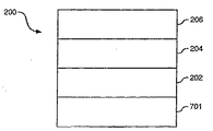
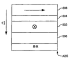
CPPスピンバルブまたは擬スピンバルブが、上記の磁気ヘッドアセンブリ121に位置付けられる再生ヘッドの一部であってもよい。これらのスピンバルブは、GMR膜に印加さるバイアス電流が膜面に垂直であるように方向付けられる。図2は、CPPスピンバルブまたは擬スピンバルブの一部の概略断面図を示す。図のように、GMRセンサ200は、強磁性フリー層206、強磁性リファレンス層202、強磁性フリー層206と強磁性リファレンス層202の間に配置されたスペーサ層204を含む。センス電流212は、GMRセンサ200の面に垂直である(すなわち、電流は積層内を垂直に流れる)。強磁性フリー層206と強磁性リファレンス層202の磁化のデフォルトでの向きまたは方向が示されている。「デフォルトでの」向きとは、再生ヘッドの外部の磁界の影響を受けない、強磁性層の磁化の方向である。
磁気再生ヘッドの一般的な加工では、GMRセンサ200に対してCMPが施される。1つのステップで、複数のGMRセンサ200を含むウェハが液体スラリの中に置かれ、研磨ディスクで研磨されてABSが形成される。このラッピング工程では、スペーサ層204が腐食性材料に曝される可能性がある。
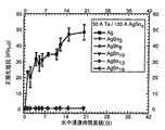
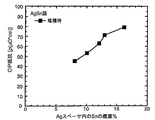
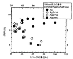
CPP−GMR再生センサの信号対雑音比は、十分に大きなバイアス電圧を使用した時に、スピントルクにより誘発される励起と高い電子流密度に起因する雑音によって制限される。このスピントルクによる励起は、主として強磁性層202、206とスペーサ層204との界面で起こる。Agを含むスペーサ層204は最近、ホイスラ合金を含む強磁性層202、206との界面が有利な状態にあるため、高いCPP−GMR信号を取得するのに特に好適であることが明らかとなっているが、スピントルクによる励起が依然として、電位差および、その結果としてGMRセンサ200に印加されるかもしれない電流を制限する。

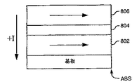
図7A〜Cは、GMRセンサの製造方法を示す。図7Aにおいて、強磁性リファレンス層202が基板701の上に堆積される。基板701は、CPP−GMR再生ヘッドを製造する際に有益な他の複数の層、たとえばニッケル鉄(NiFe)、チタン(Ta)、ルテニウム(Ru)、コバルト鉄(CoFe)または、センサの結晶構造または特性を改善するのに役立つその他の磁性または非磁性下地層等を含んでいてもよい。
112 磁気ディスク
113 スライダ
114 スピンドル
115 サスペンション
118 ドライブモータ
119 アクチュエータアーム
121 磁気ヘッドアセンブリ
122 ディスク表面
123、128 ライン
125 記録チャネル
127 アクチュエータ手段
129 制御ユニット
200 GMRセンサ
202、802、902 強磁性リファレンス層
204、804、904 スペーサ層
206、806 強磁性フリー層
212 センス電流
701 基板
808、908 反強磁性層
810、910 反強磁性結合層
812 固定強磁性層
906 第一の強磁性フリー層
912 第二の強磁性フリー層
Claims (6)
- 第1磁性層および第2磁性層、
前記第1磁性層と前記第2磁性層との間に配置されたスペーサ層であって、AgSn6、AgSn10、AgSn13、AgSn16からなるグループから選択された物質を含む、スペーサ層、
を備え、
前記スペーサ層の電気抵抗率は、30μΩ−cm以上である
ことを特徴とする再生ヘッドセンサ。 - 前記第1磁性層と前記第2磁性層の双方は、ホイスラー合金を含む
ことを特徴とする請求項1記載の再生ヘッドセンサ。 - 前記スペーサ層の厚さは、20〜50オングストロームである
ことを特徴とする請求項1記載の再生ヘッドセンサ。 - 第1磁性層および第2磁性層、
前記第1磁性層と前記第2磁性層との間に配置されたスペーサ層であって、AgSn6、AgSn10、AgSn13、AgSn16からなるグループから選択された物質を含む、スペーサ層、
を備えることを特徴とする再生ヘッドセンサ。 - 前記スペーサ層の厚さは、20〜50オングストロームである
ことを特徴とする請求項4記載の再生ヘッドセンサ。 - 前記スペーサ層の電気抵抗率は、30μΩ−cmより大きい
ことを特徴とする請求項4記載の再生ヘッドセンサ。
Applications Claiming Priority (2)
| Application Number | Priority Date | Filing Date | Title |
|---|---|---|---|
| US13/222,827 | 2011-08-31 | ||
| US13/222,827 US8743511B2 (en) | 2011-08-31 | 2011-08-31 | CPP-GMR sensor with corrosion resistent spacer layer and higher signal/noise ratio |
Publications (3)
| Publication Number | Publication Date |
|---|---|
| JP2013054814A JP2013054814A (ja) | 2013-03-21 |
| JP2013054814A5 JP2013054814A5 (ja) | 2015-09-17 |
| JP5813601B2 true JP5813601B2 (ja) | 2015-11-17 |
Family
ID=47744153
Family Applications (1)
| Application Number | Title | Priority Date | Filing Date |
|---|---|---|---|
| JP2012189572A Expired - Fee Related JP5813601B2 (ja) | 2011-08-31 | 2012-08-30 | 耐食性スペーサ層を備え、より高い信号雑音比を有するcpp−gmrセンサ |
Country Status (2)
| Country | Link |
|---|---|
| US (1) | US8743511B2 (ja) |
| JP (1) | JP5813601B2 (ja) |
Families Citing this family (7)
| Publication number | Priority date | Publication date | Assignee | Title |
|---|---|---|---|---|
| JP2014146405A (ja) * | 2013-01-30 | 2014-08-14 | Toshiba Corp | 磁気抵抗効果型の磁気ヘッドおよび磁気記録再生装置 |
| US9047891B1 (en) | 2014-05-03 | 2015-06-02 | HGST Netherlands B.V. | Current-perpendicular-to-the-plane giant magnetoresistance (CPP-GMR) sensor with indium-zinc-oxide (IZO) spacer layer |
| US9437222B1 (en) * | 2015-05-30 | 2016-09-06 | HGST Netherlands B.V. | Spin torque oscillator with high spin torque efficiency and reliability |
| US10782153B2 (en) | 2016-03-08 | 2020-09-22 | Analog Devices Global | Multiturn sensor arrangement and readout |
| US11460521B2 (en) | 2019-03-18 | 2022-10-04 | Analog Devices International Unlimited Company | Multiturn sensor arrangement |
| US11181602B2 (en) | 2019-06-10 | 2021-11-23 | International Business Machines Corporation | Detecting damaged TMR sensors using bias currents and outliers |
| US10964350B2 (en) | 2019-07-09 | 2021-03-30 | International Business Machines Corporation | Setting bias currents and limiting corrosion in TMR sensors |
Family Cites Families (13)
| Publication number | Priority date | Publication date | Assignee | Title |
|---|---|---|---|---|
| US5000779A (en) * | 1988-05-18 | 1991-03-19 | Leach & Garner | Palladium based powder-metal alloys and method for making same |
| JP3337732B2 (ja) | 1992-12-28 | 2002-10-21 | ティーディーケイ株式会社 | 磁気抵抗効果素子 |
| US5491600A (en) * | 1994-05-04 | 1996-02-13 | International Business Machines Corporation | Multi-layer conductor leads in a magnetoresistive head |
| EP0685746A3 (en) | 1994-05-30 | 1996-12-04 | Sony Corp | Magnetoresistive effect device having improved thermal resistance. |
| US5793279A (en) * | 1996-08-26 | 1998-08-11 | Read-Rite Corporation | Methods and compositions for optimizing interfacial properties of magnetoresistive sensors |
| KR20030011361A (ko) * | 2000-06-22 | 2003-02-07 | 마쯔시다덴기산교 가부시키가이샤 | 자기 저항 효과 소자와 이것을 이용한 자기 저항 효과형헤드 및 자기 기록 재생 장치 |
| US6686068B2 (en) * | 2001-02-21 | 2004-02-03 | International Business Machines Corporation | Heterogeneous spacers for CPP GMR stacks |
| US6707084B2 (en) | 2002-02-06 | 2004-03-16 | Micron Technology, Inc. | Antiferromagnetically stabilized pseudo spin valve for memory applications |
| US6876522B2 (en) | 2002-04-18 | 2005-04-05 | Seagate Technology Llc | GMR spin valve structure using heusler alloy |
| JP2006005277A (ja) | 2004-06-21 | 2006-01-05 | Alps Electric Co Ltd | 磁気検出素子 |
| JP4309363B2 (ja) | 2005-03-16 | 2009-08-05 | 株式会社東芝 | 磁気抵抗効果素子、磁気再生ヘッド及び磁気情報再生装置 |
| US7558028B2 (en) * | 2005-11-16 | 2009-07-07 | Hitachi Global Storage Technologies Netherlands B.V. | Magnetic head with improved CPP sensor using Heusler alloys |
| JP5661995B2 (ja) | 2008-12-15 | 2015-01-28 | エイチジーエスティーネザーランドビーブイ | 磁気抵抗効果型磁気ヘッド |
-
2011
- 2011-08-31 US US13/222,827 patent/US8743511B2/en active Active
-
2012
- 2012-08-30 JP JP2012189572A patent/JP5813601B2/ja not_active Expired - Fee Related
Also Published As
| Publication number | Publication date |
|---|---|
| US20130052484A1 (en) | 2013-02-28 |
| US8743511B2 (en) | 2014-06-03 |
| JP2013054814A (ja) | 2013-03-21 |
Similar Documents
| Publication | Publication Date | Title |
|---|---|---|
| JP4487472B2 (ja) | 磁気抵抗効果素子、及びこれを備える磁気ヘッド、磁気記録装置、磁気メモリ | |
| US7751156B2 (en) | Dual-layer free layer in a tunneling magnetoresistance (TMR) element | |
| JP4082274B2 (ja) | 磁気センサ及びそれを備える磁気ヘッド | |
| KR100261385B1 (ko) | 반평행 구속층과 개선된 바이어스층을 갖는 스핀 밸브 자기저항 센서와 그 센서를 이용한 자기 기록 시스템 | |
| US8760818B1 (en) | Systems and methods for providing magnetic storage elements with high magneto-resistance using heusler alloys | |
| US6313973B1 (en) | Laminated magnetorestrictive element of an exchange coupling film, an antiferromagnetic film and a ferromagnetic film and a magnetic disk drive using same | |
| JP4731393B2 (ja) | 磁気再生ヘッド | |
| JP4128938B2 (ja) | 磁気ヘッド及び磁気記録再生装置 | |
| US8379350B2 (en) | CPP-type magnetoresistive element including spacer layer | |
| JP5813601B2 (ja) | 耐食性スペーサ層を備え、より高い信号雑音比を有するcpp−gmrセンサ | |
| US7739787B2 (en) | Method of manufacturing a magnetoresistive element | |
| US8648589B2 (en) | Magnetoresistive sensor employing nitrogenated Cu/Ag under-layers with (100) textured growth as templates for CoFe, CoFeX, and Co2(MnFe)X alloys | |
| US7535682B2 (en) | Magneto-resistance element and thin film magnetic head with improved heat reliability | |
| US7599157B2 (en) | Current-perpendicular-to-the-plane (CPP) magnetoresistive sensor with high-resistivity amorphous ferromagnetic layers | |
| US9013837B2 (en) | Magnetoresistive element including a changing composition as distance increases away from an intermediate film, and magnetic head with the same | |
| JP2012216275A (ja) | 改善された硬質磁性体バイアス構造を備える面垂直電流(cpp)磁気抵抗(mr)センサ | |
| US6876523B2 (en) | Magnetic head, and the magnetic read-write devices, and the magnetic memory with magnetic sensors | |
| CN101067933A (zh) | 电流垂直平面磁致电阻传感器 | |
| JP2015015068A (ja) | 結晶性CoFeX層およびホイスラー型合金層を含む、多重層からなる基準層を含む平面垂直通電型(CPP)磁気抵抗センサ | |
| JP2004214251A (ja) | 磁気抵抗効果素子、及びそれを備える磁気ヘッド並びに磁気記録再生装置 | |
| US7895731B2 (en) | Method for manufacturing magnetic field detecting element utilizing diffusion and migration of silver | |
| US20160307587A1 (en) | Underlayer for reference layer of polycrystalline cpp gmr sensor stack | |
| US10950260B1 (en) | Magnetoresistive sensor with improved magnetic properties and magnetostriction control | |
| US8068315B2 (en) | Current perpendicular to plane GMR and TMR sensors with improved magnetic properties using Ru/Si seed layers | |
| JP2008041163A (ja) | 垂直通電型磁気抵抗効果型ヘッド |
Legal Events
| Date | Code | Title | Description |
|---|---|---|---|
| A521 | Request for written amendment filed |
Free format text: JAPANESE INTERMEDIATE CODE: A523 Effective date: 20150731 |
|
| A621 | Written request for application examination |
Free format text: JAPANESE INTERMEDIATE CODE: A621 Effective date: 20150731 |
|
| A871 | Explanation of circumstances concerning accelerated examination |
Free format text: JAPANESE INTERMEDIATE CODE: A871 Effective date: 20150731 |
|
| A975 | Report on accelerated examination |
Free format text: JAPANESE INTERMEDIATE CODE: A971005 Effective date: 20150828 |
|
| TRDD | Decision of grant or rejection written | ||
| A01 | Written decision to grant a patent or to grant a registration (utility model) |
Free format text: JAPANESE INTERMEDIATE CODE: A01 Effective date: 20150908 |
|
| A61 | First payment of annual fees (during grant procedure) |
Free format text: JAPANESE INTERMEDIATE CODE: A61 Effective date: 20150916 |
|
| R150 | Certificate of patent or registration of utility model |
Ref document number: 5813601 Country of ref document: JP Free format text: JAPANESE INTERMEDIATE CODE: R150 |
|
| R250 | Receipt of annual fees |
Free format text: JAPANESE INTERMEDIATE CODE: R250 |
|
| R250 | Receipt of annual fees |
Free format text: JAPANESE INTERMEDIATE CODE: R250 |
|
| R250 | Receipt of annual fees |
Free format text: JAPANESE INTERMEDIATE CODE: R250 |
|
| S111 | Request for change of ownership or part of ownership |
Free format text: JAPANESE INTERMEDIATE CODE: R313113 |
|
| R350 | Written notification of registration of transfer |
Free format text: JAPANESE INTERMEDIATE CODE: R350 |
|
| R250 | Receipt of annual fees |
Free format text: JAPANESE INTERMEDIATE CODE: R250 |
|
| R250 | Receipt of annual fees |
Free format text: JAPANESE INTERMEDIATE CODE: R250 |
|
| R250 | Receipt of annual fees |
Free format text: JAPANESE INTERMEDIATE CODE: R250 |
|
| LAPS | Cancellation because of no payment of annual fees |