JP5798283B2 - Vacuum chuck heater with axial symmetry and uniform thermal profile - Google Patents
Vacuum chuck heater with axial symmetry and uniform thermal profile Download PDFInfo
- Publication number
- JP5798283B2 JP5798283B2 JP2008196676A JP2008196676A JP5798283B2 JP 5798283 B2 JP5798283 B2 JP 5798283B2 JP 2008196676 A JP2008196676 A JP 2008196676A JP 2008196676 A JP2008196676 A JP 2008196676A JP 5798283 B2 JP5798283 B2 JP 5798283B2
- Authority
- JP
- Japan
- Prior art keywords
- vacuum chuck
- heater
- circular groove
- grooves
- vacuum
- Prior art date
- Legal status (The legal status is an assumption and is not a legal conclusion. Google has not performed a legal analysis and makes no representation as to the accuracy of the status listed.)
- Active
Links
Images


Classifications
-
- H—ELECTRICITY
- H01—ELECTRIC ELEMENTS
- H01L—SEMICONDUCTOR DEVICES NOT COVERED BY CLASS H10
- H01L21/00—Processes or apparatus adapted for the manufacture or treatment of semiconductor or solid state devices or of parts thereof
- H01L21/67—Apparatus specially adapted for handling semiconductor or electric solid state devices during manufacture or treatment thereof; Apparatus specially adapted for handling wafers during manufacture or treatment of semiconductor or electric solid state devices or components ; Apparatus not specifically provided for elsewhere
- H01L21/683—Apparatus specially adapted for handling semiconductor or electric solid state devices during manufacture or treatment thereof; Apparatus specially adapted for handling wafers during manufacture or treatment of semiconductor or electric solid state devices or components ; Apparatus not specifically provided for elsewhere for supporting or gripping
- H01L21/687—Apparatus specially adapted for handling semiconductor or electric solid state devices during manufacture or treatment thereof; Apparatus specially adapted for handling wafers during manufacture or treatment of semiconductor or electric solid state devices or components ; Apparatus not specifically provided for elsewhere for supporting or gripping using mechanical means, e.g. chucks, clamps or pinches
-
- C—CHEMISTRY; METALLURGY
- C23—COATING METALLIC MATERIAL; COATING MATERIAL WITH METALLIC MATERIAL; CHEMICAL SURFACE TREATMENT; DIFFUSION TREATMENT OF METALLIC MATERIAL; COATING BY VACUUM EVAPORATION, BY SPUTTERING, BY ION IMPLANTATION OR BY CHEMICAL VAPOUR DEPOSITION, IN GENERAL; INHIBITING CORROSION OF METALLIC MATERIAL OR INCRUSTATION IN GENERAL
- C23C—COATING METALLIC MATERIAL; COATING MATERIAL WITH METALLIC MATERIAL; SURFACE TREATMENT OF METALLIC MATERIAL BY DIFFUSION INTO THE SURFACE, BY CHEMICAL CONVERSION OR SUBSTITUTION; COATING BY VACUUM EVAPORATION, BY SPUTTERING, BY ION IMPLANTATION OR BY CHEMICAL VAPOUR DEPOSITION, IN GENERAL
- C23C16/00—Chemical coating by decomposition of gaseous compounds, without leaving reaction products of surface material in the coating, i.e. chemical vapour deposition [CVD] processes
- C23C16/44—Chemical coating by decomposition of gaseous compounds, without leaving reaction products of surface material in the coating, i.e. chemical vapour deposition [CVD] processes characterised by the method of coating
- C23C16/458—Chemical coating by decomposition of gaseous compounds, without leaving reaction products of surface material in the coating, i.e. chemical vapour deposition [CVD] processes characterised by the method of coating characterised by the method used for supporting substrates in the reaction chamber
- C23C16/4582—Rigid and flat substrates, e.g. plates or discs
- C23C16/4583—Rigid and flat substrates, e.g. plates or discs the substrate being supported substantially horizontally
- C23C16/4586—Elements in the interior of the support, e.g. electrodes, heating or cooling devices
-
- C—CHEMISTRY; METALLURGY
- C23—COATING METALLIC MATERIAL; COATING MATERIAL WITH METALLIC MATERIAL; CHEMICAL SURFACE TREATMENT; DIFFUSION TREATMENT OF METALLIC MATERIAL; COATING BY VACUUM EVAPORATION, BY SPUTTERING, BY ION IMPLANTATION OR BY CHEMICAL VAPOUR DEPOSITION, IN GENERAL; INHIBITING CORROSION OF METALLIC MATERIAL OR INCRUSTATION IN GENERAL
- C23C—COATING METALLIC MATERIAL; COATING MATERIAL WITH METALLIC MATERIAL; SURFACE TREATMENT OF METALLIC MATERIAL BY DIFFUSION INTO THE SURFACE, BY CHEMICAL CONVERSION OR SUBSTITUTION; COATING BY VACUUM EVAPORATION, BY SPUTTERING, BY ION IMPLANTATION OR BY CHEMICAL VAPOUR DEPOSITION, IN GENERAL
- C23C16/00—Chemical coating by decomposition of gaseous compounds, without leaving reaction products of surface material in the coating, i.e. chemical vapour deposition [CVD] processes
- C23C16/44—Chemical coating by decomposition of gaseous compounds, without leaving reaction products of surface material in the coating, i.e. chemical vapour deposition [CVD] processes characterised by the method of coating
- C23C16/458—Chemical coating by decomposition of gaseous compounds, without leaving reaction products of surface material in the coating, i.e. chemical vapour deposition [CVD] processes characterised by the method of coating characterised by the method used for supporting substrates in the reaction chamber
- C23C16/4582—Rigid and flat substrates, e.g. plates or discs
- C23C16/4583—Rigid and flat substrates, e.g. plates or discs the substrate being supported substantially horizontally
- C23C16/4584—Rigid and flat substrates, e.g. plates or discs the substrate being supported substantially horizontally the substrate being rotated
-
- Y—GENERAL TAGGING OF NEW TECHNOLOGICAL DEVELOPMENTS; GENERAL TAGGING OF CROSS-SECTIONAL TECHNOLOGIES SPANNING OVER SEVERAL SECTIONS OF THE IPC; TECHNICAL SUBJECTS COVERED BY FORMER USPC CROSS-REFERENCE ART COLLECTIONS [XRACs] AND DIGESTS
- Y10—TECHNICAL SUBJECTS COVERED BY FORMER USPC
- Y10T—TECHNICAL SUBJECTS COVERED BY FORMER US CLASSIFICATION
- Y10T279/00—Chucks or sockets
- Y10T279/11—Vacuum
Description
発明の分野
[0001]本発明の実施形態は、一般的に、半導体製造に使用される真空チャックに関し、より詳細には、改善された熱プロファイルを有する真空チャック型ヒーターに関する。
Field of Invention
[0001] Embodiments of the present invention generally relate to vacuum chucks used in semiconductor manufacturing and, more particularly, to vacuum chuck type heaters with improved thermal profiles.
関連技術の説明
[0002]準常圧化学気相堆積(SACVD)処理は、減圧(又は準常圧)において実施される。減圧は、望ましくない気相反応を減ずる傾向にあり、それにより、ウエハに亘る膜均一性を改善することができる。多くの従来のSACVD処理は、膜及び/又は被覆の高い純度及び均一性、及び適合ステップカバレージを与えることができる。
Explanation of related technology
[0002] A quasi-atmospheric chemical vapor deposition (SACVD) process is performed at reduced pressure (or quasi-atmospheric pressure). Depressurization tends to reduce undesirable gas phase reactions, thereby improving film uniformity across the wafer. Many conventional SACVD processes can provide high purity and uniformity of the film and / or coating, and adaptive step coverage.
[0003]しかしながら、ある特定の適用例においては、従来のSACVD処理では、堆積膜の厚さ非均一性が望ましくない程に高くなってしまい、品質及び歩留りが減少してしまうことが観察されている。このような厚さ非均一性は、少なくともある部分において、前述した処理に伴う基板の非均一熱プロファイルによるものであると考えられる。この基板の非均一熱プロファイルは、少なくともある部分において、真空チャック型ヒーターと基板との間の非均一熱移送によるものである。 [0003] However, in certain applications, it has been observed that conventional SACVD processing results in undesirably high deposited film thickness non-uniformity, reducing quality and yield. Yes. Such thickness non-uniformity is believed to be due, at least in part, to the non-uniform thermal profile of the substrate associated with the processing described above. This non-uniform thermal profile of the substrate is due, at least in part, to non-uniform heat transfer between the vacuum chuck heater and the substrate.
[0004]真空チャック型ヒーターは、一般的に、ヒーターを埋め込んだ基板支持体を含み、この基板支持体には、1つ以上の溝及び真空チャッキング孔が形成されており、これら溝及び真空チャッキング孔は、ワークピースが配置されるとき、それらの溝に真空を維持することでそのワークピース(例えば、半導体ウエハ)を基板支持体上に保持するようにするためのものである。従来、真空チャック型ヒーターに形成された溝及びチャッキング孔は、強い真空チャッキングパワーを与える以外、従来の真空チャック型ヒーター上に置かれた基板に堆積される膜の品質に相当な影響を与えるものとは考えられていなかった。しかしながら、本発明者等は、それら溝及びチャッキング孔のサイズ及び位置が、その上に置かれた基板に生ずる熱プロファイルに対して、以前に認識されていたよりも大きな影響を与えることを見出したのである。更に又、本発明者等は、このような従来のヒーターから生じる熱プロファイルが、このような基板に堆積される膜の膜厚さに変化をもたらしてしまう程に非均一であることを見出したのである。ある処理においては、例えば、熱プロファイルが1度変化すると、そこに堆積される膜の厚さが約60−100オングストローム/分も変化してしまう。従って、このような従来の真空チャック型ヒーターを使用して基板上に堆積される膜の厚さプロファイルは、特に、その堆積膜の全厚さが減少するとき、このような非均一熱プロファイルのため大きく変化してしまう。 [0004] A vacuum chuck type heater generally includes a substrate support in which the heater is embedded, the substrate support having one or more grooves and vacuum chucking holes formed therein, the grooves and the vacuum. The chucking holes are intended to hold the workpiece (eg, semiconductor wafer) on the substrate support by maintaining a vacuum in the grooves when the workpiece is placed. Conventionally, the grooves and chucking holes formed in the vacuum chuck type heater have a considerable influence on the quality of the film deposited on the substrate placed on the conventional vacuum chuck type heater, in addition to giving a strong vacuum chucking power. It was not considered to give. However, the present inventors have found that the size and location of these grooves and chucking holes have a greater impact than previously recognized on the thermal profile produced in the substrate placed thereon. It is. Furthermore, the inventors have found that the thermal profile resulting from such a conventional heater is non-uniform enough to cause a change in the film thickness of the film deposited on such a substrate. It is. In some processes, for example, if the thermal profile changes once, the thickness of the film deposited there will change by about 60-100 angstroms / minute. Thus, the thickness profile of a film deposited on a substrate using such a conventional vacuum chuck heater is such that, particularly when the total thickness of the deposited film is reduced, such a non-uniform thermal profile. Therefore, it will change greatly.
[0005]例えば、従来においては、1つの考え方として、基板と支持体との間の強いチャッキング力を与えることにより、それらの間の熱接触を高め、それにより、基板の熱プロファイルを改善し、基板上に堆積される膜の特性を改善しようとするものがあった。従って、従来の真空チャックでは、望ましい高い真空チャッキングパワーを得るため大きなチャッキング孔(例えば、直径約3.0mm)を設けていた。しかしながら、本発明者等は、これらチャッキング孔に対応する位置において基板上に相当な「クールスポット」が発生してしまうことがあることを見出したのである。また、本発明者等は、真空溝の交差部にチャッキング孔を配設すると(従来においては、種々な溝内の真空圧をより効果的に分散することができると考えられていた)、実際には、このような「クールスポット」現象が増長させられてしまうことを見出したのである。 [0005] For example, in the prior art, one idea is to provide a strong chucking force between the substrate and the support to increase the thermal contact between them, thereby improving the thermal profile of the substrate. Some have attempted to improve the properties of the film deposited on the substrate. Therefore, in the conventional vacuum chuck, a large chucking hole (for example, a diameter of about 3.0 mm ) is provided in order to obtain a desired high vacuum chucking power. However, the present inventors have found that a considerable “cool spot” may occur on the substrate at a position corresponding to these chucking holes. In addition, the present inventors provided a chucking hole at the intersection of the vacuum grooves (conventionally, it was thought that the vacuum pressure in various grooves could be more effectively dispersed) In fact, they have found that this “cool spot” phenomenon is exacerbated.
[0006]従来のチャッキング孔のサイズ及び位置によって生ぜしめられる「クールスポット」に加えて、本発明者等は、更に、ある従来の溝パターンの非軸対称配列により、基板上の温度プロファイルが非軸対称とされてしまい、従って、膜厚さプロファイルが非軸対称とされてしまうことを見出したのである。 [0006] In addition to the “cool spots” created by the size and location of conventional chucking holes, the inventors have further demonstrated that the temperature profile on the substrate is reduced by the non-axisymmetric arrangement of certain conventional groove patterns. It has been found that the film thickness is non-axisymmetric, and therefore the film thickness profile is non-axisymmetric.
[0007]その上、本発明者等は、更に、ヒーター毎の変化により堆積される膜の厚さに大きな影響があることを見出したのである。例えば、処理チャンバ内のヒーターを交換するとき(故障や保守等のため)、その交換したヒーターは、交換前のヒーターとは同じ厚さプロファイルを与えないことがある。更に又、このようなヒーター毎の変化は、異なる真空ヒーターチャックを各々有する複数の処理チャンバに亘って処理標準化をすることを不可能又は非常に困難なものとしてしまうことがある。 [0007] In addition, the present inventors have further found that the thickness of the deposited film is greatly affected by changes from heater to heater. For example, when replacing a heater in a processing chamber (due to failure, maintenance, etc.), the replaced heater may not give the same thickness profile as the heater before replacement. Furthermore, such changes from heater to heater may make it impossible or very difficult to standardize processing across multiple processing chambers each having a different vacuum heater chuck.
[0008]真空チャック型ヒーターを使用する従来のあるシステムは、基板上の非均一熱プロファイルを補償するように処理チャンバ内又は真空チャック型ヒーター内のガスの流量を制御しているが、ヒーター毎に熱プロファイルが変化するのでは、そのような補償が難しくなってしまう。 [0008] Some conventional systems that use vacuum chuck type heaters control the flow rate of gas in the processing chamber or in the vacuum chuck type heater to compensate for the non-uniform thermal profile on the substrate. However, if the thermal profile changes, such compensation becomes difficult.
[0009]従って、当業分野においては、基板を処理するための改良された真空チャック型ヒーターが必要とされている。 [0009] Accordingly, there is a need in the art for an improved vacuum chuck type heater for processing substrates.
[0010]軸対称及び/又はより均一な熱プロファイルを有する真空チャックの実施形態が提供される。ある実施形態では、真空チャックは、基板を支持するための支持表面を有する本体と、上記支持表面に形成された複数の軸対称に配置された溝であって、上記溝のうちの少なくとも幾つかは交差しているような複数の溝と、上記本体を通して且つ上記溝内に形成され且つ上記溝の非交差部分に配設され、動作中に上記溝を真空源に流体結合するための複数のチャッキング孔と、を含む。 [0010] Embodiments of vacuum chucks having axisymmetric and / or more uniform thermal profiles are provided. In one embodiment, the vacuum chuck includes a body having a support surface for supporting a substrate, and a plurality of axially arranged grooves formed in the support surface, wherein at least some of the grooves A plurality of intersecting grooves and a plurality of grooves formed through and into the groove and disposed at non-intersecting portions of the grooves for fluidly coupling the grooves to a vacuum source during operation. A chucking hole.
[0011]ある実施形態では、基板処理チャンバは、処理チャンバと、上記処理チャンバ内に配設された真空チャックとを含み、上記真空チャックは、基板を支持するための支持表面を有する本体と、上記支持表面に形成された複数の軸対称に配置された溝であって、上記溝のうちの少なくとも幾つかは交差しているような複数の溝と、上記本体を通して且つ上記溝内に形成され且つ上記溝の非交差部分に配設され、動作中に上記溝を真空源に流体結合するための複数のチャッキング孔と、を含む。 [0011] In an embodiment, a substrate processing chamber includes a processing chamber and a vacuum chuck disposed within the processing chamber, the vacuum chuck having a body having a support surface for supporting a substrate; A plurality of axisymmetrically disposed grooves formed in the support surface, wherein at least some of the grooves intersect, and are formed through and into the body. And a plurality of chucking holes disposed in non-intersecting portions of the groove for fluidly coupling the groove to a vacuum source during operation.
[0012]本発明の別の態様では、真空チャックを製造するための方法が提供される。ある実施形態では、真空チャックを製造するための方法は、基板支持表面を有する本体を準備するステップと、上記支持表面に複数の軸対称に配置された溝を形成するステップと、上記溝の非交差部分内に上記本体を通して複数のチャッキング孔を形成するステップと、を含む。 [0012] In another aspect of the invention, a method for manufacturing a vacuum chuck is provided. In one embodiment, a method for manufacturing a vacuum chuck includes providing a body having a substrate support surface, forming a plurality of axisymmetrically disposed grooves in the support surface, and non-grooving of the grooves. Forming a plurality of chucking holes through the body in the intersection.
[0013]本発明の前述したような特徴を詳細に理解できるように、概要について簡単に前述したような本発明について、幾つかを添付図面に例示している実施形態に関して、以下より特定して説明する。しかしながら、添付図面は、本発明の典型的な実施形態のみを例示しているのであって、従って、本発明の範囲をそれに限定しようとしているものではなく、本発明は、均等の効果を発揮しうる他の実施形態を含みうるものであることに、注意されたい。 [0013] In order that the foregoing features of the invention may be more fully understood, the invention as briefly described above in terms of overview, with respect to the embodiments illustrated in the accompanying drawings, will be identified more particularly below. explain. However, the accompanying drawings illustrate only typical embodiments of the present invention, and thus are not intended to limit the scope of the present invention, and the present invention exhibits equivalent effects. It should be noted that other embodiments may be included.
[0017]理解を容易とするため、図において共通な同一の要素を示すのに、可能な限り、同一の参照符号を使用している。これら図は、同一縮尺で描かれておらず、明瞭なものとするため簡単化されている。1つの実施形態の要素及び特徴は、更に繰り返し述べなくとも、他の実施形態に効果的に組み込むことができるものと考えられる。 [0017] To facilitate understanding, identical reference numerals have been used, where possible, to designate identical, common elements in the figures. These figures are not drawn to scale and have been simplified for clarity. It is contemplated that the elements and features of one embodiment can be effectively incorporated into other embodiments without further recitation.
[0018]本発明の実施形態は、軸対称及び/又はより均一な熱プロファイルを有する真空チャック型ヒーターを提供する。ここに使用する用語「熱プロファイル」は、真空チャック型ヒーター上に置かれ望ましい温度まで加熱される基板又はワークピースの定常状態温度を指している。ここに使用される用語「軸対称」は、真空チャック型ヒーター又はその上に置かれた基板の中心軸、例えば、半導体ウエハ又は基板の中心から垂直に延長する軸、に対して熱プロファイルが対称であることを指している。 [0018] Embodiments of the present invention provide a vacuum chuck type heater having an axisymmetric and / or more uniform thermal profile. As used herein, the term “thermal profile” refers to the steady state temperature of a substrate or workpiece that is placed on a vacuum chuck type heater and heated to the desired temperature. As used herein, the term “axisymmetric” means that the thermal profile is symmetric with respect to the central axis of the vacuum chuck heater or the substrate placed thereon, eg, an axis extending perpendicularly from the center of the semiconductor wafer or substrate. It points to that.
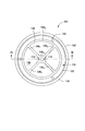
[0019]図1A及び図1Bは、それぞれ、本発明のある実施形態による真空チャック型ヒーター100の上面図及び切断線1B−1Bに沿って取った断面側面図を示している。この真空チャック型ヒーター100は、基板、例えば、半導体基板(これに限定されるのではないが、200mm又は300mm半導体基板の如き)を処理するのに使用するための処理チャンバ(図示していない)に配設することができる。この真空チャック型ヒーター100は、化学気相堆積(CVD)、物理気相堆積(PVD)等の如き、基板を加熱する必要のあるような任意の処理に使用することができる。ここに説明するような真空チャック型ヒーターを使用して効果のある、適した処理チャンバとしては、例えば、PRODUCER(登録商標名)半導体処理システムにおいて使用される処理チャンバの準常圧CVD(SACVD)ラインがある。これらは、全てカリフォルニア州サンタクララのアプライドマテリアル社から入手可能なものである。本発明の真空チャック型ヒーターは、他の処理チャンバ及びシステムにも使用することができると考えられる。
[0019] FIGS. 1A and 1B show a top view and a cross-sectional side view taken along
[0020]この真空チャック型ヒーター100は、ヒーター112(抵抗加熱素子等の如き)を配設した本体102と、この本体102を支持するためのシャフト104とを備える。本体102は、窒化アルミニウム、酸化アルミニウム、ステンレス鋼、アルミニウム、熱分解窒化ホウ素等の如き処理条件に耐えるに適した任意の材料で形成することができる。本体102は、その上に基板を支持するための実質的に平坦な支持表面106を有している。ある実施形態では、処理中に基板が配置されるポケット120を画成するための周辺突出部又はリップ118が設けられる。このリップ118は、処理中に基板を中心合わせし且つ望ましい位置に保持するようにする特徴部122(傾斜側壁部の如き)を有するとよい。支持表面106から基板を上昇させ、また、支持表面106上へと基板を下降させるようにするリフトピン(図示していない)に対応させて、複数のリフトピン孔124が設けられている(図1A及び図1Bにおいては、3つのリフトピン孔124が示されている)。
The vacuum
[0021]ヒーター112は、一般的に、本体102に埋め込まれた1つ以上の抵抗コイル(図示していない)を備える。それらの抵抗コイルは、ヒーターゾーンを生成するように独立して制御できるものであるとよい。処理温度を監視するため、温度指示計(図示していない)が設けられるとよい。一実施例として、この温度指示計は、支持表面106での(又はその上に置かれた基板の表面での)温度に相関したデータを与えるように配置された熱電対(図示していない)であってよい。
[0021] The
[0022]ある実施形態では、高周波電極116が、高周波電力をチャンバに結合すること又はチャンバから高周波電力を除去するため高周波接地路を与えること、のうちの1つ又は両方を行うため、本体102内に設けられる。
[0022] In some embodiments, the high-
[0023]真空チャッキングを行うため、1つ以上の溝108が支持表面106に形成され、複数のチャッキング孔110が溝108内に設けられている。それら溝108は、本体102を形成するための成形、鋳造又は燒結処理中に及び/又は本体102の支持表面106の機械加工によるが如き任意の適当な仕方において形成することができる。これらの溝108は、従来の真空ヒーターチャックに、既存の溝を除去し(その支持表面を充填し又は機械加工するようにして)、そして、ここに説明した教示に従って溝108を機械加工することにより、形成することもできる(又は真空ヒーターチャック100を改造することもできる)。
[0023] To perform vacuum chucking, one or
[0024]本発明のある実施形態では、チャッキング孔110は、従来の真空ヒーターチャックに比較して、減少した直径を有しており、それにより、「クールスポット」効果を除去又は減少させるようにしている。ある実施形態では、チャッキング孔110は、約1.016mm以下の直径、又は約0.762mmから1.524mmの間の直径、又は約1.016mmの直径を有している。
[0024] In an embodiment of the present invention, the chucking
[0025]本発明のある実施形態では、チャッキング孔110は、各溝108の交差部から離れた位置に配設される(例えば、チャッキング孔110は、溝の非交差部分に配設される)。ある実施形態では、チャッキング孔110は、(必ずしも軸対称ではないが)対称的に配置される。例えば、図1A及び図1Bに示した実施形態では、溝108内の直径方向において対向した位置に設けられ且つ溝108の最も近い交差部から等距離だけ離間して、1対のチャッキング孔110が設けられている。溝内の異なる位置(但し、前述したように、溝交差部内でないこと)に他のより多い又はより少ないチャッキング孔110を設けることができると考えられる。
[0025] In some embodiments of the present invention, the chucking holes 110 are disposed at a location away from the intersection of each groove 108 (eg, the chucking holes 110 are disposed at non-intersecting portions of the grooves). ) In some embodiments, the chucking holes 110 are arranged symmetrically (although not necessarily axially symmetric). For example, in the embodiment shown in FIGS. 1A and 1B, a pair of chucking
[0026]本発明のある実施形態では、溝108は、真空チャック型ヒーター100の中心軸150の周りに軸対称において配置されており、それにより、軸対称熱プロファイルを生成することができ、従って、軸対称膜厚さプロファイルを生成することができる。例えば、図1A及び図1Bに示した実施形態では、内側円形溝108B及び外側円形溝108Aが設けられ、この内側円形溝108Bと外側円形溝108Aとを接続する4つの等距離離間した半径方向溝108C、108D、108E及び108Fが設けられている。同じ又は異なる数の溝を有する他の軸対称幾何学的構成を使用することもできると考えられる。
[0026] In an embodiment of the present invention, the
[0027]これらの軸対称に配置された溝108により、基板と真空ヒーターチャック100の支持表面106との間のガス圧を均一分布させることができる。これにより、真空ヒーターチャック100と基板との間に均一な熱移送がなされ、その結果、基板のより均一な温度プロファイルを生ぜしめることができる。例えば、テスト結果によれば、真空ヒーターチャック100上に置かれた基板の方位温度範囲が、6℃から約3℃より低い温度まで減少され、それにより、熱プロファイル非均一性を補償するため他の手段に頼らなければならない程度を減少させることができることが示されている。
[0027] These axially arranged
[0028]本発明のある実施形態では、溝108の公差を厳しいものとすることにより、ヒーター毎の温度プロファイル変化を効果的に減ずることができる。例えば、ある実施形態では、溝108は、約0.4318mmから0.5842mmの間の幅を有する。ある実施形態では、溝108は、約0.0635mmから0.0889mmの間の深さを有する。その上、ある実施形態では、支持表面106は、約0.8128μmより小さな、又は約0.7112μmから0.8128μmの間の減少した表面粗さを有し、それにより、使用中の基板と支持表面106との間の表面接触を改善することができる。こうして、基板温度のヒーター毎の変化は、真空ヒーターチャック100の表面の形状状態を厳しく制御することにより制御される。
[0028] In one embodiment of the present invention, tighter tolerances in the
[0029]シャフト104は、チャッキング孔110(及び、従って溝108)を真空システム(図示していない)に流体結合する複数の開口114(又はチューブ、ホース等の如き他の機構)を有する。従って、動作において、基板が真空ヒーターチャック100の支持表面106上に置かれ、チャッキング孔110を通して溝108内に真空圧を加え維持することにより、その基板はその支持表面106上に保持される。シャフト104は、更に、真空ヒーターチャック100の本体102へのファシリティー又はコネクタのルーティングを行うための中心通路126を備える。例えば、ヒーター112を動作するための電気接続を与えるための1つ以上のヒーターコネクタ128が、その通路126を通してルーティングされ、そのヒーター112に結合される。更に又、高周波電極116を高周波電力供給源又は接地接続部(図示せず)に結合するための高周波コネクタ130がその通路126を通してルーティングされる。
[0029] The
[0030]図2は、本発明のある実施形態による真空チャック型ヒーターを製造するための方法200のフローチャートを示している。この方法200は、図1A及び図1Bに関して前述した真空チャック型ヒーター100について説明される。ある実施形態では、この方法200は、基板支持表面106を有する本体102を準備するステップ202で開始される。本体102は、前述したような任意の適当な材料で形成され、成形、燒結、機械加工等の如き適当な仕方で形成されてよい。
[0030] FIG. 2 shows a flowchart of a
[0031]次に、ステップ204において、支持表面106に複数の軸対称に配置された溝108が形成される。これら溝108は、本体102を形成するための製造処理中の如き任意の適当な仕方で形成されてよい。別の仕方として、溝108は、後で本体102の支持表面106へそれら溝を機械加工することにより形成されてもよい。既存の真空チャック型ヒーターの改造のような、ある実施形態では、それら溝108を形成する前に、以前からあった溝を本体102から除去する。例えば、ある実施形態では、支持表面106は、以前からあった溝を除去するため平らに機械加工される。以前からあった溝のうちのあるものは、溝108を形成するのに完全に除去されるのでなく、再調整されるようにしてもよいことが考えられる。
[0031] Next, in
[0032]次に、ステップ206において、複数のチャッキング孔110が、溝108の非交差部分内に本体を通して形成される。これらチャッキング孔110は、溝108の形成前又は後に形成することができる。更に又、真空チャック型ヒーターを改造するような実施形態では、それらチャッキング孔110は、本体102内に既に存在していてもよいし、又は後で形成されてもよい。また、真空チャック型ヒーターを改造するような実施形態においては、チャッキング孔110を形成する前に、以前からあったチャッキング孔を少なくとも部分的に充填するようにしてもよい。
[0032] Next, at
[0033]こうして、軸対称及び均一熱プロファイルの真空チャック型ヒーターの実施形態が提供される。この真空チャック型ヒーターによれば、この真空チャック型ヒーター上に置かれた基板上に形成される膜及び/又は被覆の厚さ非均一性が効果的に最少とされる。その上、ここに説明した本発明の真空チャック型ヒーターによれば、1)チャッキング孔に対応する基板上に局部コールドスポットによって生ずる膜圧さスパイクの減少、2)真空チャック型ヒーターの熱プロファイルの非対称性によって生ずる膜厚さプロファイルの非対称性の減少、及び3)ヒーター毎の熱プロファイルの変化の減少、のうちの1つ以上を効果的に達成することができる。 [0033] Thus, embodiments of an axisymmetric and uniform thermal profile vacuum chuck type heater are provided. According to this vacuum chuck type heater, the thickness non-uniformity of the film and / or coating formed on the substrate placed on this vacuum chuck type heater is effectively minimized. Moreover, according to the vacuum chuck heater of the present invention described herein, 1) reduction of film pressure spikes caused by local cold spots on the substrate corresponding to the chucking hole, 2) thermal profile of the vacuum chuck heater One or more of the reduction in thickness profile asymmetry caused by the asymmetry and 3) reduction in thermal profile change from heater to heater can be effectively achieved.
[0034]本発明の実施形態について前述してきたのであるが、本発明の基本的範囲から逸脱せずに、本発明の他の更なる実施形態を考えることができるものであり、本発明の範囲は、特許請求の範囲の記載によって決定される。 [0034] While embodiments of the invention have been described above, other and further embodiments of the invention can be devised without departing from the basic scope thereof, and the scope of the invention Is determined by the claims.
100…真空チャック型ヒーター(真空ヒーターチャック)、102…本体、104…シャフト、106…支持表面、108…溝、108A…外側円形溝、108B…内側円形溝、108C…半径方向溝、108D…半径方向溝、108E…半径方向溝、108F…半径方向溝、110…チャッキング孔、112…ヒーター、114…開口、116…高周波電極、118…周辺突出部(リップ)、120…ポケット、122…特徴部(傾斜側壁部)、124…リフトピン孔、126…中心通路、128…ヒーターコネクタ、130…高周波コネクタ、150…中心軸
100 ... vacuum chuck type heater (vacuum heater chuck), 102 ... main body, 104 ... shaft, 106 ...
Claims (14)
基板を支持するための支持表面を有する本体と、
上記本体内に配設されたヒーターと、
上記支持表面に形成され、上記真空チャック型ヒーターの中心軸の周りに対称に配置された複数の軸対称溝と、を備え、上記複数の軸対称溝は、
上記真空チャック型ヒーターの中心軸の周りに配置された内側円形溝と、
上記内側円形溝の周りに同心で配置された外側円形溝と、
上記内側円形溝と上記外側円形溝とを接続する複数の半径方向溝と、を含み、
上記真空チャック型ヒーターは更に、上記本体を通して且つ上記内側円形溝内のみに形成され且つ上記複数の軸対称溝の非交差部分に配設され、動作中に上記複数の軸対称溝を真空システムに流体結合するための複数のチャッキング孔、を備え、上記複数のチャッキング孔は、上記真空チャック型ヒーターの中心軸の周りに対称に配置されている真空チャック型ヒーター。 A vacuum chuck type heater ,
A body having a support surface for supporting the substrate;
A heater disposed in the main body,
A plurality of axisymmetric grooves formed on the support surface and arranged symmetrically around a central axis of the vacuum chuck heater , the plurality of axisymmetric grooves,
An inner circular groove disposed around the central axis of the vacuum chuck heater ;
An outer circular groove disposed concentrically around the inner circular groove;
A plurality of radial grooves connecting the inner circular groove and the outer circular groove;
The vacuum chuck heater is further formed through the body and only in the inner circular groove and disposed at a non-intersecting portion of the plurality of axisymmetric grooves, and the plurality of axisymmetric grooves into the vacuum system during operation. a plurality of chucking hole for fluidly coupling comprises a plurality of chucking holes, a vacuum chuck type heater disposed symmetrically about a central axis of said vacuum chuck type heater.
上記処理チャンバ内に配設された、請求項1から9のいずれか1項に記載の真空チャック型ヒーターと、
を備える基板処理チャンバ。 A processing chamber;
The vacuum chuck heater according to any one of claims 1 to 9 , which is disposed in the processing chamber;
A substrate processing chamber comprising:
基板支持表面を有する本体と、上記本体内に配設されたヒーターとを準備するステップと、
上記支持表面に上記真空チャック型ヒーターの中心軸の周りに対称に配置された複数の軸対称溝を形成するステップと、を備え、上記複数の軸対称溝は、
上記真空チャック型ヒーターの中心軸の周りに配置された内側円形溝と、
上記内側円形溝の周りに同心で配置された外側円形溝と、
上記内側円形溝と上記外側円形溝とを接続する複数の半径方向溝と、を含み、
上記方法は更に、上記内側円形溝のみに、且つ複数の軸対称溝の非交差部分内に上記本体を通して複数のチャッキング孔を形成するステップ、を備え、上記複数のチャッキング孔は、上記真空チャック型ヒーターの中心軸の周りに対称に配置されている方法。 In a method for manufacturing a vacuum chuck type heater ,
Providing a body having a substrate support surface and a heater disposed in the body ;
Forming a plurality of axisymmetric grooves symmetrically arranged around the central axis of the vacuum chuck heater on the support surface, and the plurality of axisymmetric grooves,
An inner circular groove disposed around the central axis of the vacuum chuck heater ;
An outer circular groove disposed concentrically around the inner circular groove;
A plurality of radial grooves connecting the inner circular groove and the outer circular groove;
The method further comprises forming a plurality of chucking holes through the body only in the inner circular groove and in non-intersecting portions of the plurality of axisymmetric grooves, the plurality of chucking holes being in the vacuum. The method is arranged symmetrically around the central axis of the chuck heater .
Applications Claiming Priority (2)
| Application Number | Priority Date | Filing Date | Title |
|---|---|---|---|
| US11/830,589 | 2007-07-30 | ||
| US11/830,589 US20090031955A1 (en) | 2007-07-30 | 2007-07-30 | Vacuum chucking heater of axisymmetrical and uniform thermal profile |
Related Child Applications (1)
| Application Number | Title | Priority Date | Filing Date |
|---|---|---|---|
| JP2013259036A Division JP2014053645A (en) | 2007-07-30 | 2013-12-16 | Vacuum chucking heater of axisymmetrical and uniform thermal profile |
Publications (3)
| Publication Number | Publication Date |
|---|---|
| JP2009033178A JP2009033178A (en) | 2009-02-12 |
| JP2009033178A5 JP2009033178A5 (en) | 2011-09-15 |
| JP5798283B2 true JP5798283B2 (en) | 2015-10-21 |
Family
ID=40330933
Family Applications (2)
| Application Number | Title | Priority Date | Filing Date |
|---|---|---|---|
| JP2008196676A Active JP5798283B2 (en) | 2007-07-30 | 2008-07-30 | Vacuum chuck heater with axial symmetry and uniform thermal profile |
| JP2013259036A Withdrawn JP2014053645A (en) | 2007-07-30 | 2013-12-16 | Vacuum chucking heater of axisymmetrical and uniform thermal profile |
Family Applications After (1)
| Application Number | Title | Priority Date | Filing Date |
|---|---|---|---|
| JP2013259036A Withdrawn JP2014053645A (en) | 2007-07-30 | 2013-12-16 | Vacuum chucking heater of axisymmetrical and uniform thermal profile |
Country Status (6)
| Country | Link |
|---|---|
| US (1) | US20090031955A1 (en) |
| JP (2) | JP5798283B2 (en) |
| KR (2) | KR101062595B1 (en) |
| CN (1) | CN101358338B (en) |
| SG (1) | SG149792A1 (en) |
| TW (1) | TWI491757B (en) |
Families Citing this family (35)
| Publication number | Priority date | Publication date | Assignee | Title |
|---|---|---|---|---|
| US8198567B2 (en) | 2008-01-15 | 2012-06-12 | Applied Materials, Inc. | High temperature vacuum chuck assembly |
| US8637794B2 (en) | 2009-10-21 | 2014-01-28 | Lam Research Corporation | Heating plate with planar heating zones for semiconductor processing |
| US8791392B2 (en) | 2010-10-22 | 2014-07-29 | Lam Research Corporation | Methods of fault detection for multiplexed heater array |
| US8546732B2 (en) * | 2010-11-10 | 2013-10-01 | Lam Research Corporation | Heating plate with planar heater zones for semiconductor processing |
| DE102010055675A1 (en) * | 2010-12-22 | 2012-06-28 | Fraunhofer-Gesellschaft zur Förderung der angewandten Forschung e.V. | Holding device for substrates and method for coating a substrate |
| US11171008B2 (en) | 2011-03-01 | 2021-11-09 | Applied Materials, Inc. | Abatement and strip process chamber in a dual load lock configuration |
| JP6054314B2 (en) | 2011-03-01 | 2016-12-27 | アプライド マテリアルズ インコーポレイテッドApplied Materials,Incorporated | Method and apparatus for substrate transport and radical confinement |
| CN103403852B (en) | 2011-03-01 | 2016-06-08 | 应用材料公司 | The elimination of double; two load locks configuration and lift-off processing chamber |
| WO2012118606A2 (en) | 2011-03-01 | 2012-09-07 | Applied Materials, Inc. | Thin heated substrate support |
| US20120267423A1 (en) * | 2011-04-19 | 2012-10-25 | Taiwan Semiconductor Manufacturing Company, Ltd. | Methods and Apparatus for Thin Die Processing |
| US10242890B2 (en) * | 2011-08-08 | 2019-03-26 | Applied Materials, Inc. | Substrate support with heater |
| DE102012100825A1 (en) * | 2011-12-01 | 2013-06-06 | solar-semi GmbH | Apparatus for processing a substrate and method therefor |
| KR102068186B1 (en) | 2012-02-29 | 2020-02-11 | 어플라이드 머티어리얼스, 인코포레이티드 | Abatement and strip process chamber in a load lock configuration |
| US9478447B2 (en) * | 2012-11-26 | 2016-10-25 | Applied Materials, Inc. | Substrate support with wire mesh plasma containment |
| CN104637854B (en) * | 2013-11-13 | 2018-12-07 | 沈阳新松机器人自动化股份有限公司 | It is a kind of for adsorbing the sucker of silicon wafer |
| KR20230116078A (en) * | 2014-05-21 | 2023-08-03 | 어플라이드 머티어리얼스, 인코포레이티드 | Thermal processing susceptor |
| CN105161449A (en) * | 2014-05-30 | 2015-12-16 | 盛美半导体设备(上海)有限公司 | Wafer fixing device |
| KR101477660B1 (en) * | 2014-08-01 | 2014-12-31 | (주)지원에프알에스 | Article of footwear improving restoring force of cushion column by using elastic ring and elastic band |
| JP6394337B2 (en) | 2014-12-04 | 2018-09-26 | 株式会社Sumco | Adsorption chuck, chamfering polishing apparatus, and silicon wafer chamfering polishing method |
| US9728437B2 (en) | 2015-02-03 | 2017-08-08 | Applied Materials, Inc. | High temperature chuck for plasma processing systems |
| US9691645B2 (en) | 2015-08-06 | 2017-06-27 | Applied Materials, Inc. | Bolted wafer chuck thermal management systems and methods for wafer processing systems |
| US9741593B2 (en) | 2015-08-06 | 2017-08-22 | Applied Materials, Inc. | Thermal management systems and methods for wafer processing systems |
| JP6674800B2 (en) * | 2016-03-07 | 2020-04-01 | 日本特殊陶業株式会社 | Substrate support device |
| KR102523850B1 (en) * | 2016-07-11 | 2023-04-21 | 주식회사 미코세라믹스 | Chuck structure and apparatus for separating chips having the chuck structure |
| JP6847610B2 (en) * | 2016-09-14 | 2021-03-24 | 株式会社Screenホールディングス | Heat treatment equipment |
| US10468290B2 (en) * | 2016-11-02 | 2019-11-05 | Ultratech, Inc. | Wafer chuck apparatus with micro-channel regions |
| JP6829118B2 (en) * | 2017-03-16 | 2021-02-10 | 株式会社日本製鋼所 | Laser irradiation device, laser irradiation method, and manufacturing method of semiconductor device |
| KR102339350B1 (en) * | 2017-04-03 | 2021-12-16 | 주식회사 미코세라믹스 | Ceramic heater |
| WO2019076553A1 (en) * | 2017-10-19 | 2019-04-25 | Evatec Ag | Method and apparatus for treating a substrate |
| US11361981B2 (en) * | 2018-05-02 | 2022-06-14 | Applied Materials, Inc. | Batch substrate support with warped substrate capability |
| JP6959201B2 (en) * | 2018-08-29 | 2021-11-02 | 日本碍子株式会社 | Ceramic heater |
| CN109280904A (en) * | 2018-11-27 | 2019-01-29 | 中山德华芯片技术有限公司 | A kind of graphite plate applied to lattice mismatched structures epitaxial growth |
| CN111490002B (en) * | 2020-04-21 | 2023-06-27 | 錼创显示科技股份有限公司 | Carrier plate structure |
| CN115142050B (en) * | 2022-09-05 | 2022-11-25 | 拓荆科技(北京)有限公司 | Vacuum adsorption heating plate and device |
| CN115354307B (en) * | 2022-09-23 | 2023-08-18 | 拓荆科技股份有限公司 | Vacuum heating substrate equipment |
Family Cites Families (28)
| Publication number | Priority date | Publication date | Assignee | Title |
|---|---|---|---|---|
| US4183545A (en) * | 1978-07-28 | 1980-01-15 | Advanced Simiconductor Materials/America | Rotary vacuum-chuck using no rotary union |
| JPH01134945A (en) * | 1987-11-19 | 1989-05-26 | Tokyo Electron Ltd | Wafer holding device |
| JP2908516B2 (en) * | 1990-05-07 | 1999-06-21 | キヤノン株式会社 | Vacuum suction type wafer holding device |
| JPH06244269A (en) * | 1992-09-07 | 1994-09-02 | Mitsubishi Electric Corp | Semiconductor manufacturing apparatus, wafer vacuum chuck device thereof, and gas cleaning and nitride film formation therefor |
| US5800686A (en) * | 1993-04-05 | 1998-09-01 | Applied Materials, Inc. | Chemical vapor deposition chamber with substrate edge protection |
| JPH0722496A (en) * | 1993-06-29 | 1995-01-24 | Nikon Corp | Device for sucking and holding substrate |
| US5342068A (en) * | 1993-08-26 | 1994-08-30 | Texas Instruments Incorporated | Laminar flow vacuum chuck |
| JPH10116760A (en) * | 1996-10-08 | 1998-05-06 | Nikon Corp | Aligner and substrate holding device |
| TW524873B (en) * | 1997-07-11 | 2003-03-21 | Applied Materials Inc | Improved substrate supporting apparatus and processing chamber |
| US5989444A (en) * | 1998-02-13 | 1999-11-23 | Zywno; Marek | Fluid bearings and vacuum chucks and methods for producing same |
| US6179924B1 (en) * | 1998-04-28 | 2001-01-30 | Applied Materials, Inc. | Heater for use in substrate processing apparatus to deposit tungsten |
| US6241825B1 (en) * | 1999-04-16 | 2001-06-05 | Cutek Research Inc. | Compliant wafer chuck |
| US6464795B1 (en) * | 1999-05-21 | 2002-10-15 | Applied Materials, Inc. | Substrate support member for a processing chamber |
| JP2001144197A (en) * | 1999-11-11 | 2001-05-25 | Fujitsu Ltd | Semiconductor device, manufacturing method therefor, and testing method |
| JP2002057209A (en) * | 2000-06-01 | 2002-02-22 | Tokyo Electron Ltd | Single-wafer processing apparatus and single-wafer processing method |
| KR100523113B1 (en) * | 2000-06-01 | 2005-10-19 | 동경 엘렉트론 주식회사 | Single-substrate-processing apparatus for semiconductor process |
| US6413321B1 (en) * | 2000-12-07 | 2002-07-02 | Applied Materials, Inc. | Method and apparatus for reducing particle contamination on wafer backside during CVD process |
| KR20030001842A (en) * | 2001-06-28 | 2003-01-08 | 삼성전자 주식회사 | Probe chuck in electrical die sorting apparatus |
| JP2004009165A (en) * | 2002-06-04 | 2004-01-15 | Ngk Spark Plug Co Ltd | Sucking chuck |
| JP2004039978A (en) * | 2002-07-05 | 2004-02-05 | Hirata Corp | Substrate holding device |
| US20040016745A1 (en) * | 2002-07-29 | 2004-01-29 | Applied Materials, Inc. | Method for achieving process uniformity by modifying thermal coupling between heater and substrate |
| DE10235482B3 (en) * | 2002-08-02 | 2004-01-22 | Süss Microtec Lithography Gmbh | Device for fixing thin and flexible substrates |
| JP4090313B2 (en) * | 2002-09-11 | 2008-05-28 | 大日本スクリーン製造株式会社 | Substrate holding device and substrate processing apparatus |
| KR20040103648A (en) * | 2003-05-30 | 2004-12-09 | 삼성전자주식회사 | Chuck for supporting a substrate and apparatus for manufacturing thin film having the same |
| JP2006005095A (en) * | 2004-06-16 | 2006-01-05 | Ngk Insulators Ltd | Substrate heater and its manufacturing process |
| JP2006310697A (en) * | 2005-05-02 | 2006-11-09 | Dainippon Screen Mfg Co Ltd | Vacuum chuck |
| KR200405748Y1 (en) * | 2005-10-27 | 2006-01-11 | (주)쎄미시스코 | Vacuum chuck of dual industrial structure that use porous silicon |
| JP5019811B2 (en) * | 2006-07-20 | 2012-09-05 | 東京エレクトロン株式会社 | Repair method of electrostatic adsorption electrode |
-
2007
- 2007-07-30 US US11/830,589 patent/US20090031955A1/en not_active Abandoned
-
2008
- 2008-07-24 TW TW097128157A patent/TWI491757B/en active
- 2008-07-28 SG SG200805597-2A patent/SG149792A1/en unknown
- 2008-07-29 KR KR1020080074005A patent/KR101062595B1/en active IP Right Grant
- 2008-07-30 CN CN2008101312151A patent/CN101358338B/en active Active
- 2008-07-30 JP JP2008196676A patent/JP5798283B2/en active Active
-
2011
- 2011-04-28 KR KR1020110040280A patent/KR101495513B1/en active IP Right Grant
-
2013
- 2013-12-16 JP JP2013259036A patent/JP2014053645A/en not_active Withdrawn
Also Published As
| Publication number | Publication date |
|---|---|
| CN101358338A (en) | 2009-02-04 |
| TW200923118A (en) | 2009-06-01 |
| KR20090013077A (en) | 2009-02-04 |
| JP2014053645A (en) | 2014-03-20 |
| JP2009033178A (en) | 2009-02-12 |
| KR101062595B1 (en) | 2011-09-06 |
| TWI491757B (en) | 2015-07-11 |
| SG149792A1 (en) | 2009-02-27 |
| CN101358338B (en) | 2012-05-16 |
| KR20110068955A (en) | 2011-06-22 |
| US20090031955A1 (en) | 2009-02-05 |
| KR101495513B1 (en) | 2015-03-03 |
Similar Documents
| Publication | Publication Date | Title |
|---|---|---|
| JP5798283B2 (en) | Vacuum chuck heater with axial symmetry and uniform thermal profile | |
| US11417561B2 (en) | Edge ring for a substrate processing chamber | |
| CN106469666B (en) | Base and matrix processing equipment | |
| US6464795B1 (en) | Substrate support member for a processing chamber | |
| US6464790B1 (en) | Substrate support member | |
| EP3254307B1 (en) | Radially outward pad design for electrostatic chuck surface | |
| WO2014008077A1 (en) | Substrate support for substrate backside contamination control | |
| JP2022552237A (en) | Wafer heater with backside purge and integrated ramp purge | |
| US11682576B2 (en) | Pedestal heater for spatial multi-wafer processing tool | |
| TWI690012B (en) | Wafer pedestal with heating mechanism and reaction chamber including the same | |
| JP2023507091A (en) | A semiconductor processing chuck with recesses near the perimeter of the wafer to reduce edge/center non-uniformity | |
| US11610792B2 (en) | Heated substrate support with thermal baffles | |
| KR102273563B1 (en) | Material heating method using heating device | |
| KR102141678B1 (en) | Heated substrate support | |
| US20210287929A1 (en) | Heater uniformity in substrate supports | |
| US20230011261A1 (en) | Multi-zone heater with minimum rf loss | |
| JPWO2021127272A5 (en) |
Legal Events
| Date | Code | Title | Description |
|---|---|---|---|
| RD03 | Notification of appointment of power of attorney |
Free format text: JAPANESE INTERMEDIATE CODE: A7423 Effective date: 20101111 |
|
| RD04 | Notification of resignation of power of attorney |
Free format text: JAPANESE INTERMEDIATE CODE: A7424 Effective date: 20101209 |
|
| A521 | Request for written amendment filed |
Free format text: JAPANESE INTERMEDIATE CODE: A523 Effective date: 20110801 |
|
| A621 | Written request for application examination |
Free format text: JAPANESE INTERMEDIATE CODE: A621 Effective date: 20110801 |
|
| RD04 | Notification of resignation of power of attorney |
Free format text: JAPANESE INTERMEDIATE CODE: A7424 Effective date: 20120925 |
|
| A977 | Report on retrieval |
Free format text: JAPANESE INTERMEDIATE CODE: A971007 Effective date: 20121026 |
|
| A131 | Notification of reasons for refusal |
Free format text: JAPANESE INTERMEDIATE CODE: A131 Effective date: 20121101 |
|
| A521 | Request for written amendment filed |
Free format text: JAPANESE INTERMEDIATE CODE: A523 Effective date: 20130201 |
|
| A02 | Decision of refusal |
Free format text: JAPANESE INTERMEDIATE CODE: A02 Effective date: 20130814 |
|
| A521 | Request for written amendment filed |
Free format text: JAPANESE INTERMEDIATE CODE: A523 Effective date: 20131216 |
|
| A521 | Request for written amendment filed |
Free format text: JAPANESE INTERMEDIATE CODE: A523 Effective date: 20140121 |
|
| A911 | Transfer to examiner for re-examination before appeal (zenchi) |
Free format text: JAPANESE INTERMEDIATE CODE: A911 Effective date: 20140129 |
|
| A912 | Re-examination (zenchi) completed and case transferred to appeal board |
Free format text: JAPANESE INTERMEDIATE CODE: A912 Effective date: 20140320 |
|
| A521 | Request for written amendment filed |
Free format text: JAPANESE INTERMEDIATE CODE: A523 Effective date: 20150625 |
|
| A61 | First payment of annual fees (during grant procedure) |
Free format text: JAPANESE INTERMEDIATE CODE: A61 Effective date: 20150821 |
|
| R150 | Certificate of patent or registration of utility model |
Ref document number: 5798283 Country of ref document: JP Free format text: JAPANESE INTERMEDIATE CODE: R150 |
|
| R250 | Receipt of annual fees |
Free format text: JAPANESE INTERMEDIATE CODE: R250 |
|
| R250 | Receipt of annual fees |
Free format text: JAPANESE INTERMEDIATE CODE: R250 |
|
| R250 | Receipt of annual fees |
Free format text: JAPANESE INTERMEDIATE CODE: R250 |
|
| R250 | Receipt of annual fees |
Free format text: JAPANESE INTERMEDIATE CODE: R250 |
|
| R250 | Receipt of annual fees |
Free format text: JAPANESE INTERMEDIATE CODE: R250 |