JP5795196B2 - Semiconductor package - Google Patents
Semiconductor packageInfo
- Publication number
- JP5795196B2 JP5795196B2 JP2011129230A JP2011129230A JP5795196B2 JP 5795196 B2 JP5795196 B2 JP 5795196B2 JP 2011129230 A JP2011129230 A JP 2011129230A JP 2011129230 A JP2011129230 A JP 2011129230A JP 5795196 B2 JP5795196 B2 JP 5795196B2
- Authority
- JP
- Japan
- Prior art keywords
- wiring pattern
- package
- recognition mark
- connection
- semiconductor element
- Prior art date
- Legal status (The legal status is an assumption and is not a legal conclusion. Google has not performed a legal analysis and makes no representation as to the accuracy of the status listed.)
- Active
Links
Images


Classifications
-
- H—ELECTRICITY
- H01—ELECTRIC ELEMENTS
- H01L—SEMICONDUCTOR DEVICES NOT COVERED BY CLASS H10
- H01L23/00—Details of semiconductor or other solid state devices
- H01L23/544—Marks applied to semiconductor devices or parts, e.g. registration marks, alignment structures, wafer maps
-
- H—ELECTRICITY
- H01—ELECTRIC ELEMENTS
- H01L—SEMICONDUCTOR DEVICES NOT COVERED BY CLASS H10
- H01L25/00—Assemblies consisting of a plurality of individual semiconductor or other solid state devices ; Multistep manufacturing processes thereof
- H01L25/03—Assemblies consisting of a plurality of individual semiconductor or other solid state devices ; Multistep manufacturing processes thereof all the devices being of a type provided for in the same subgroup of groups H01L27/00 - H01L33/00, or in a single subclass of H10K, H10N, e.g. assemblies of rectifier diodes
- H01L25/10—Assemblies consisting of a plurality of individual semiconductor or other solid state devices ; Multistep manufacturing processes thereof all the devices being of a type provided for in the same subgroup of groups H01L27/00 - H01L33/00, or in a single subclass of H10K, H10N, e.g. assemblies of rectifier diodes the devices having separate containers
- H01L25/105—Assemblies consisting of a plurality of individual semiconductor or other solid state devices ; Multistep manufacturing processes thereof all the devices being of a type provided for in the same subgroup of groups H01L27/00 - H01L33/00, or in a single subclass of H10K, H10N, e.g. assemblies of rectifier diodes the devices having separate containers the devices being of a type provided for in group H01L27/00
-
- H—ELECTRICITY
- H01—ELECTRIC ELEMENTS
- H01L—SEMICONDUCTOR DEVICES NOT COVERED BY CLASS H10
- H01L25/00—Assemblies consisting of a plurality of individual semiconductor or other solid state devices ; Multistep manufacturing processes thereof
- H01L25/50—Multistep manufacturing processes of assemblies consisting of devices, each device being of a type provided for in group H01L27/00 or H01L29/00
-
- H—ELECTRICITY
- H01—ELECTRIC ELEMENTS
- H01L—SEMICONDUCTOR DEVICES NOT COVERED BY CLASS H10
- H01L2224/00—Indexing scheme for arrangements for connecting or disconnecting semiconductor or solid-state bodies and methods related thereto as covered by H01L24/00
- H01L2224/01—Means for bonding being attached to, or being formed on, the surface to be connected, e.g. chip-to-package, die-attach, "first-level" interconnects; Manufacturing methods related thereto
- H01L2224/10—Bump connectors; Manufacturing methods related thereto
- H01L2224/15—Structure, shape, material or disposition of the bump connectors after the connecting process
- H01L2224/16—Structure, shape, material or disposition of the bump connectors after the connecting process of an individual bump connector
- H01L2224/161—Disposition
- H01L2224/16151—Disposition the bump connector connecting between a semiconductor or solid-state body and an item not being a semiconductor or solid-state body, e.g. chip-to-substrate, chip-to-passive
- H01L2224/16221—Disposition the bump connector connecting between a semiconductor or solid-state body and an item not being a semiconductor or solid-state body, e.g. chip-to-substrate, chip-to-passive the body and the item being stacked
- H01L2224/16225—Disposition the bump connector connecting between a semiconductor or solid-state body and an item not being a semiconductor or solid-state body, e.g. chip-to-substrate, chip-to-passive the body and the item being stacked the item being non-metallic, e.g. insulating substrate with or without metallisation
- H01L2224/16237—Disposition the bump connector connecting between a semiconductor or solid-state body and an item not being a semiconductor or solid-state body, e.g. chip-to-substrate, chip-to-passive the body and the item being stacked the item being non-metallic, e.g. insulating substrate with or without metallisation the bump connector connecting to a bonding area disposed in a recess of the surface of the item
-
- H—ELECTRICITY
- H01—ELECTRIC ELEMENTS
- H01L—SEMICONDUCTOR DEVICES NOT COVERED BY CLASS H10
- H01L2224/00—Indexing scheme for arrangements for connecting or disconnecting semiconductor or solid-state bodies and methods related thereto as covered by H01L24/00
- H01L2224/01—Means for bonding being attached to, or being formed on, the surface to be connected, e.g. chip-to-package, die-attach, "first-level" interconnects; Manufacturing methods related thereto
- H01L2224/10—Bump connectors; Manufacturing methods related thereto
- H01L2224/15—Structure, shape, material or disposition of the bump connectors after the connecting process
- H01L2224/16—Structure, shape, material or disposition of the bump connectors after the connecting process of an individual bump connector
- H01L2224/161—Disposition
- H01L2224/16151—Disposition the bump connector connecting between a semiconductor or solid-state body and an item not being a semiconductor or solid-state body, e.g. chip-to-substrate, chip-to-passive
- H01L2224/16221—Disposition the bump connector connecting between a semiconductor or solid-state body and an item not being a semiconductor or solid-state body, e.g. chip-to-substrate, chip-to-passive the body and the item being stacked
- H01L2224/16225—Disposition the bump connector connecting between a semiconductor or solid-state body and an item not being a semiconductor or solid-state body, e.g. chip-to-substrate, chip-to-passive the body and the item being stacked the item being non-metallic, e.g. insulating substrate with or without metallisation
- H01L2224/16238—Disposition the bump connector connecting between a semiconductor or solid-state body and an item not being a semiconductor or solid-state body, e.g. chip-to-substrate, chip-to-passive the body and the item being stacked the item being non-metallic, e.g. insulating substrate with or without metallisation the bump connector connecting to a bonding area protruding from the surface of the item
-
- H—ELECTRICITY
- H01—ELECTRIC ELEMENTS
- H01L—SEMICONDUCTOR DEVICES NOT COVERED BY CLASS H10
- H01L2224/00—Indexing scheme for arrangements for connecting or disconnecting semiconductor or solid-state bodies and methods related thereto as covered by H01L24/00
- H01L2224/01—Means for bonding being attached to, or being formed on, the surface to be connected, e.g. chip-to-package, die-attach, "first-level" interconnects; Manufacturing methods related thereto
- H01L2224/26—Layer connectors, e.g. plate connectors, solder or adhesive layers; Manufacturing methods related thereto
- H01L2224/31—Structure, shape, material or disposition of the layer connectors after the connecting process
- H01L2224/32—Structure, shape, material or disposition of the layer connectors after the connecting process of an individual layer connector
- H01L2224/321—Disposition
- H01L2224/32135—Disposition the layer connector connecting between different semiconductor or solid-state bodies, i.e. chip-to-chip
- H01L2224/32145—Disposition the layer connector connecting between different semiconductor or solid-state bodies, i.e. chip-to-chip the bodies being stacked
-
- H—ELECTRICITY
- H01—ELECTRIC ELEMENTS
- H01L—SEMICONDUCTOR DEVICES NOT COVERED BY CLASS H10
- H01L2224/00—Indexing scheme for arrangements for connecting or disconnecting semiconductor or solid-state bodies and methods related thereto as covered by H01L24/00
- H01L2224/01—Means for bonding being attached to, or being formed on, the surface to be connected, e.g. chip-to-package, die-attach, "first-level" interconnects; Manufacturing methods related thereto
- H01L2224/26—Layer connectors, e.g. plate connectors, solder or adhesive layers; Manufacturing methods related thereto
- H01L2224/31—Structure, shape, material or disposition of the layer connectors after the connecting process
- H01L2224/32—Structure, shape, material or disposition of the layer connectors after the connecting process of an individual layer connector
- H01L2224/321—Disposition
- H01L2224/32151—Disposition the layer connector connecting between a semiconductor or solid-state body and an item not being a semiconductor or solid-state body, e.g. chip-to-substrate, chip-to-passive
- H01L2224/32221—Disposition the layer connector connecting between a semiconductor or solid-state body and an item not being a semiconductor or solid-state body, e.g. chip-to-substrate, chip-to-passive the body and the item being stacked
- H01L2224/32225—Disposition the layer connector connecting between a semiconductor or solid-state body and an item not being a semiconductor or solid-state body, e.g. chip-to-substrate, chip-to-passive the body and the item being stacked the item being non-metallic, e.g. insulating substrate with or without metallisation
-
- H—ELECTRICITY
- H01—ELECTRIC ELEMENTS
- H01L—SEMICONDUCTOR DEVICES NOT COVERED BY CLASS H10
- H01L2224/00—Indexing scheme for arrangements for connecting or disconnecting semiconductor or solid-state bodies and methods related thereto as covered by H01L24/00
- H01L2224/01—Means for bonding being attached to, or being formed on, the surface to be connected, e.g. chip-to-package, die-attach, "first-level" interconnects; Manufacturing methods related thereto
- H01L2224/42—Wire connectors; Manufacturing methods related thereto
- H01L2224/47—Structure, shape, material or disposition of the wire connectors after the connecting process
- H01L2224/48—Structure, shape, material or disposition of the wire connectors after the connecting process of an individual wire connector
- H01L2224/4805—Shape
- H01L2224/4809—Loop shape
- H01L2224/48091—Arched
-
- H—ELECTRICITY
- H01—ELECTRIC ELEMENTS
- H01L—SEMICONDUCTOR DEVICES NOT COVERED BY CLASS H10
- H01L2224/00—Indexing scheme for arrangements for connecting or disconnecting semiconductor or solid-state bodies and methods related thereto as covered by H01L24/00
- H01L2224/01—Means for bonding being attached to, or being formed on, the surface to be connected, e.g. chip-to-package, die-attach, "first-level" interconnects; Manufacturing methods related thereto
- H01L2224/42—Wire connectors; Manufacturing methods related thereto
- H01L2224/47—Structure, shape, material or disposition of the wire connectors after the connecting process
- H01L2224/48—Structure, shape, material or disposition of the wire connectors after the connecting process of an individual wire connector
- H01L2224/481—Disposition
- H01L2224/48151—Connecting between a semiconductor or solid-state body and an item not being a semiconductor or solid-state body, e.g. chip-to-substrate, chip-to-passive
- H01L2224/48221—Connecting between a semiconductor or solid-state body and an item not being a semiconductor or solid-state body, e.g. chip-to-substrate, chip-to-passive the body and the item being stacked
- H01L2224/48225—Connecting between a semiconductor or solid-state body and an item not being a semiconductor or solid-state body, e.g. chip-to-substrate, chip-to-passive the body and the item being stacked the item being non-metallic, e.g. insulating substrate with or without metallisation
- H01L2224/48227—Connecting between a semiconductor or solid-state body and an item not being a semiconductor or solid-state body, e.g. chip-to-substrate, chip-to-passive the body and the item being stacked the item being non-metallic, e.g. insulating substrate with or without metallisation connecting the wire to a bond pad of the item
- H01L2224/48229—Connecting between a semiconductor or solid-state body and an item not being a semiconductor or solid-state body, e.g. chip-to-substrate, chip-to-passive the body and the item being stacked the item being non-metallic, e.g. insulating substrate with or without metallisation connecting the wire to a bond pad of the item the bond pad protruding from the surface of the item
-
- H—ELECTRICITY
- H01—ELECTRIC ELEMENTS
- H01L—SEMICONDUCTOR DEVICES NOT COVERED BY CLASS H10
- H01L2224/00—Indexing scheme for arrangements for connecting or disconnecting semiconductor or solid-state bodies and methods related thereto as covered by H01L24/00
- H01L2224/73—Means for bonding being of different types provided for in two or more of groups H01L2224/10, H01L2224/18, H01L2224/26, H01L2224/34, H01L2224/42, H01L2224/50, H01L2224/63, H01L2224/71
- H01L2224/732—Location after the connecting process
- H01L2224/73201—Location after the connecting process on the same surface
- H01L2224/73203—Bump and layer connectors
- H01L2224/73204—Bump and layer connectors the bump connector being embedded into the layer connector
-
- H—ELECTRICITY
- H01—ELECTRIC ELEMENTS
- H01L—SEMICONDUCTOR DEVICES NOT COVERED BY CLASS H10
- H01L2224/00—Indexing scheme for arrangements for connecting or disconnecting semiconductor or solid-state bodies and methods related thereto as covered by H01L24/00
- H01L2224/73—Means for bonding being of different types provided for in two or more of groups H01L2224/10, H01L2224/18, H01L2224/26, H01L2224/34, H01L2224/42, H01L2224/50, H01L2224/63, H01L2224/71
- H01L2224/732—Location after the connecting process
- H01L2224/73251—Location after the connecting process on different surfaces
- H01L2224/73265—Layer and wire connectors
-
- H—ELECTRICITY
- H01—ELECTRIC ELEMENTS
- H01L—SEMICONDUCTOR DEVICES NOT COVERED BY CLASS H10
- H01L2224/00—Indexing scheme for arrangements for connecting or disconnecting semiconductor or solid-state bodies and methods related thereto as covered by H01L24/00
- H01L2224/80—Methods for connecting semiconductor or other solid state bodies using means for bonding being attached to, or being formed on, the surface to be connected
- H01L2224/81—Methods for connecting semiconductor or other solid state bodies using means for bonding being attached to, or being formed on, the surface to be connected using a bump connector
- H01L2224/8138—Bonding interfaces outside the semiconductor or solid-state body
- H01L2224/81399—Material
- H01L2224/814—Material with a principal constituent of the material being a metal or a metalloid, e.g. boron [B], silicon [Si], germanium [Ge], arsenic [As], antimony [Sb], tellurium [Te] and polonium [Po], and alloys thereof
- H01L2224/81438—Material with a principal constituent of the material being a metal or a metalloid, e.g. boron [B], silicon [Si], germanium [Ge], arsenic [As], antimony [Sb], tellurium [Te] and polonium [Po], and alloys thereof the principal constituent melting at a temperature of greater than or equal to 950°C and less than 1550°C
- H01L2224/81444—Gold [Au] as principal constituent
-
- H—ELECTRICITY
- H01—ELECTRIC ELEMENTS
- H01L—SEMICONDUCTOR DEVICES NOT COVERED BY CLASS H10
- H01L2224/00—Indexing scheme for arrangements for connecting or disconnecting semiconductor or solid-state bodies and methods related thereto as covered by H01L24/00
- H01L2224/80—Methods for connecting semiconductor or other solid state bodies using means for bonding being attached to, or being formed on, the surface to be connected
- H01L2224/81—Methods for connecting semiconductor or other solid state bodies using means for bonding being attached to, or being formed on, the surface to be connected using a bump connector
- H01L2224/8138—Bonding interfaces outside the semiconductor or solid-state body
- H01L2224/81399—Material
- H01L2224/814—Material with a principal constituent of the material being a metal or a metalloid, e.g. boron [B], silicon [Si], germanium [Ge], arsenic [As], antimony [Sb], tellurium [Te] and polonium [Po], and alloys thereof
- H01L2224/81438—Material with a principal constituent of the material being a metal or a metalloid, e.g. boron [B], silicon [Si], germanium [Ge], arsenic [As], antimony [Sb], tellurium [Te] and polonium [Po], and alloys thereof the principal constituent melting at a temperature of greater than or equal to 950°C and less than 1550°C
- H01L2224/81455—Nickel [Ni] as principal constituent
-
- H—ELECTRICITY
- H01—ELECTRIC ELEMENTS
- H01L—SEMICONDUCTOR DEVICES NOT COVERED BY CLASS H10
- H01L2224/00—Indexing scheme for arrangements for connecting or disconnecting semiconductor or solid-state bodies and methods related thereto as covered by H01L24/00
- H01L2224/80—Methods for connecting semiconductor or other solid state bodies using means for bonding being attached to, or being formed on, the surface to be connected
- H01L2224/83—Methods for connecting semiconductor or other solid state bodies using means for bonding being attached to, or being formed on, the surface to be connected using a layer connector
- H01L2224/831—Methods for connecting semiconductor or other solid state bodies using means for bonding being attached to, or being formed on, the surface to be connected using a layer connector the layer connector being supplied to the parts to be connected in the bonding apparatus
- H01L2224/83102—Methods for connecting semiconductor or other solid state bodies using means for bonding being attached to, or being formed on, the surface to be connected using a layer connector the layer connector being supplied to the parts to be connected in the bonding apparatus using surface energy, e.g. capillary forces
-
- H—ELECTRICITY
- H01—ELECTRIC ELEMENTS
- H01L—SEMICONDUCTOR DEVICES NOT COVERED BY CLASS H10
- H01L2224/00—Indexing scheme for arrangements for connecting or disconnecting semiconductor or solid-state bodies and methods related thereto as covered by H01L24/00
- H01L2224/80—Methods for connecting semiconductor or other solid state bodies using means for bonding being attached to, or being formed on, the surface to be connected
- H01L2224/85—Methods for connecting semiconductor or other solid state bodies using means for bonding being attached to, or being formed on, the surface to be connected using a wire connector
- H01L2224/8538—Bonding interfaces outside the semiconductor or solid-state body
- H01L2224/85399—Material
- H01L2224/854—Material with a principal constituent of the material being a metal or a metalloid, e.g. boron (B), silicon (Si), germanium (Ge), arsenic (As), antimony (Sb), tellurium (Te) and polonium (Po), and alloys thereof
- H01L2224/85438—Material with a principal constituent of the material being a metal or a metalloid, e.g. boron (B), silicon (Si), germanium (Ge), arsenic (As), antimony (Sb), tellurium (Te) and polonium (Po), and alloys thereof the principal constituent melting at a temperature of greater than or equal to 950°C and less than 1550°C
- H01L2224/85444—Gold (Au) as principal constituent
-
- H—ELECTRICITY
- H01—ELECTRIC ELEMENTS
- H01L—SEMICONDUCTOR DEVICES NOT COVERED BY CLASS H10
- H01L2224/00—Indexing scheme for arrangements for connecting or disconnecting semiconductor or solid-state bodies and methods related thereto as covered by H01L24/00
- H01L2224/80—Methods for connecting semiconductor or other solid state bodies using means for bonding being attached to, or being formed on, the surface to be connected
- H01L2224/85—Methods for connecting semiconductor or other solid state bodies using means for bonding being attached to, or being formed on, the surface to be connected using a wire connector
- H01L2224/8538—Bonding interfaces outside the semiconductor or solid-state body
- H01L2224/85399—Material
- H01L2224/854—Material with a principal constituent of the material being a metal or a metalloid, e.g. boron (B), silicon (Si), germanium (Ge), arsenic (As), antimony (Sb), tellurium (Te) and polonium (Po), and alloys thereof
- H01L2224/85438—Material with a principal constituent of the material being a metal or a metalloid, e.g. boron (B), silicon (Si), germanium (Ge), arsenic (As), antimony (Sb), tellurium (Te) and polonium (Po), and alloys thereof the principal constituent melting at a temperature of greater than or equal to 950°C and less than 1550°C
- H01L2224/85455—Nickel (Ni) as principal constituent
-
- H—ELECTRICITY
- H01—ELECTRIC ELEMENTS
- H01L—SEMICONDUCTOR DEVICES NOT COVERED BY CLASS H10
- H01L2224/00—Indexing scheme for arrangements for connecting or disconnecting semiconductor or solid-state bodies and methods related thereto as covered by H01L24/00
- H01L2224/91—Methods for connecting semiconductor or solid state bodies including different methods provided for in two or more of groups H01L2224/80 - H01L2224/90
- H01L2224/92—Specific sequence of method steps
- H01L2224/921—Connecting a surface with connectors of different types
- H01L2224/9212—Sequential connecting processes
- H01L2224/92122—Sequential connecting processes the first connecting process involving a bump connector
- H01L2224/92125—Sequential connecting processes the first connecting process involving a bump connector the second connecting process involving a layer connector
-
- H—ELECTRICITY
- H01—ELECTRIC ELEMENTS
- H01L—SEMICONDUCTOR DEVICES NOT COVERED BY CLASS H10
- H01L2225/00—Details relating to assemblies covered by the group H01L25/00 but not provided for in its subgroups
- H01L2225/03—All the devices being of a type provided for in the same subgroup of groups H01L27/00 - H01L33/648 and H10K99/00
- H01L2225/04—All the devices being of a type provided for in the same subgroup of groups H01L27/00 - H01L33/648 and H10K99/00 the devices not having separate containers
- H01L2225/065—All the devices being of a type provided for in the same subgroup of groups H01L27/00 - H01L33/648 and H10K99/00 the devices not having separate containers the devices being of a type provided for in group H01L27/00
- H01L2225/06503—Stacked arrangements of devices
- H01L2225/0651—Wire or wire-like electrical connections from device to substrate
-
- H—ELECTRICITY
- H01—ELECTRIC ELEMENTS
- H01L—SEMICONDUCTOR DEVICES NOT COVERED BY CLASS H10
- H01L2225/00—Details relating to assemblies covered by the group H01L25/00 but not provided for in its subgroups
- H01L2225/03—All the devices being of a type provided for in the same subgroup of groups H01L27/00 - H01L33/648 and H10K99/00
- H01L2225/04—All the devices being of a type provided for in the same subgroup of groups H01L27/00 - H01L33/648 and H10K99/00 the devices not having separate containers
- H01L2225/065—All the devices being of a type provided for in the same subgroup of groups H01L27/00 - H01L33/648 and H10K99/00 the devices not having separate containers the devices being of a type provided for in group H01L27/00
- H01L2225/06503—Stacked arrangements of devices
- H01L2225/06517—Bump or bump-like direct electrical connections from device to substrate
-
- H—ELECTRICITY
- H01—ELECTRIC ELEMENTS
- H01L—SEMICONDUCTOR DEVICES NOT COVERED BY CLASS H10
- H01L2225/00—Details relating to assemblies covered by the group H01L25/00 but not provided for in its subgroups
- H01L2225/03—All the devices being of a type provided for in the same subgroup of groups H01L27/00 - H01L33/648 and H10K99/00
- H01L2225/04—All the devices being of a type provided for in the same subgroup of groups H01L27/00 - H01L33/648 and H10K99/00 the devices not having separate containers
- H01L2225/065—All the devices being of a type provided for in the same subgroup of groups H01L27/00 - H01L33/648 and H10K99/00 the devices not having separate containers the devices being of a type provided for in group H01L27/00
- H01L2225/06503—Stacked arrangements of devices
- H01L2225/06555—Geometry of the stack, e.g. form of the devices, geometry to facilitate stacking
- H01L2225/06558—Geometry of the stack, e.g. form of the devices, geometry to facilitate stacking the devices having passive surfaces facing each other, i.e. in a back-to-back arrangement
-
- H—ELECTRICITY
- H01—ELECTRIC ELEMENTS
- H01L—SEMICONDUCTOR DEVICES NOT COVERED BY CLASS H10
- H01L2225/00—Details relating to assemblies covered by the group H01L25/00 but not provided for in its subgroups
- H01L2225/03—All the devices being of a type provided for in the same subgroup of groups H01L27/00 - H01L33/648 and H10K99/00
- H01L2225/04—All the devices being of a type provided for in the same subgroup of groups H01L27/00 - H01L33/648 and H10K99/00 the devices not having separate containers
- H01L2225/065—All the devices being of a type provided for in the same subgroup of groups H01L27/00 - H01L33/648 and H10K99/00 the devices not having separate containers the devices being of a type provided for in group H01L27/00
- H01L2225/06503—Stacked arrangements of devices
- H01L2225/06555—Geometry of the stack, e.g. form of the devices, geometry to facilitate stacking
- H01L2225/06568—Geometry of the stack, e.g. form of the devices, geometry to facilitate stacking the devices decreasing in size, e.g. pyramidical stack
-
- H—ELECTRICITY
- H01—ELECTRIC ELEMENTS
- H01L—SEMICONDUCTOR DEVICES NOT COVERED BY CLASS H10
- H01L2225/00—Details relating to assemblies covered by the group H01L25/00 but not provided for in its subgroups
- H01L2225/03—All the devices being of a type provided for in the same subgroup of groups H01L27/00 - H01L33/648 and H10K99/00
- H01L2225/10—All the devices being of a type provided for in the same subgroup of groups H01L27/00 - H01L33/648 and H10K99/00 the devices having separate containers
- H01L2225/1005—All the devices being of a type provided for in the same subgroup of groups H01L27/00 - H01L33/648 and H10K99/00 the devices having separate containers the devices being of a type provided for in group H01L27/00
- H01L2225/1011—All the devices being of a type provided for in the same subgroup of groups H01L27/00 - H01L33/648 and H10K99/00 the devices having separate containers the devices being of a type provided for in group H01L27/00 the containers being in a stacked arrangement
- H01L2225/1017—All the devices being of a type provided for in the same subgroup of groups H01L27/00 - H01L33/648 and H10K99/00 the devices having separate containers the devices being of a type provided for in group H01L27/00 the containers being in a stacked arrangement the lowermost container comprising a device support
- H01L2225/1023—All the devices being of a type provided for in the same subgroup of groups H01L27/00 - H01L33/648 and H10K99/00 the devices having separate containers the devices being of a type provided for in group H01L27/00 the containers being in a stacked arrangement the lowermost container comprising a device support the support being an insulating substrate
-
- H—ELECTRICITY
- H01—ELECTRIC ELEMENTS
- H01L—SEMICONDUCTOR DEVICES NOT COVERED BY CLASS H10
- H01L2225/00—Details relating to assemblies covered by the group H01L25/00 but not provided for in its subgroups
- H01L2225/03—All the devices being of a type provided for in the same subgroup of groups H01L27/00 - H01L33/648 and H10K99/00
- H01L2225/10—All the devices being of a type provided for in the same subgroup of groups H01L27/00 - H01L33/648 and H10K99/00 the devices having separate containers
- H01L2225/1005—All the devices being of a type provided for in the same subgroup of groups H01L27/00 - H01L33/648 and H10K99/00 the devices having separate containers the devices being of a type provided for in group H01L27/00
- H01L2225/1011—All the devices being of a type provided for in the same subgroup of groups H01L27/00 - H01L33/648 and H10K99/00 the devices having separate containers the devices being of a type provided for in group H01L27/00 the containers being in a stacked arrangement
- H01L2225/1047—Details of electrical connections between containers
- H01L2225/1058—Bump or bump-like electrical connections, e.g. balls, pillars, posts
-
- H—ELECTRICITY
- H01—ELECTRIC ELEMENTS
- H01L—SEMICONDUCTOR DEVICES NOT COVERED BY CLASS H10
- H01L23/00—Details of semiconductor or other solid state devices
- H01L23/48—Arrangements for conducting electric current to or from the solid state body in operation, e.g. leads, terminal arrangements ; Selection of materials therefor
- H01L23/488—Arrangements for conducting electric current to or from the solid state body in operation, e.g. leads, terminal arrangements ; Selection of materials therefor consisting of soldered or bonded constructions
- H01L23/498—Leads, i.e. metallisations or lead-frames on insulating substrates, e.g. chip carriers
- H01L23/49811—Additional leads joined to the metallisation on the insulating substrate, e.g. pins, bumps, wires, flat leads
-
- H—ELECTRICITY
- H01—ELECTRIC ELEMENTS
- H01L—SEMICONDUCTOR DEVICES NOT COVERED BY CLASS H10
- H01L24/00—Arrangements for connecting or disconnecting semiconductor or solid-state bodies; Methods or apparatus related thereto
- H01L24/01—Means for bonding being attached to, or being formed on, the surface to be connected, e.g. chip-to-package, die-attach, "first-level" interconnects; Manufacturing methods related thereto
- H01L24/10—Bump connectors ; Manufacturing methods related thereto
- H01L24/15—Structure, shape, material or disposition of the bump connectors after the connecting process
- H01L24/16—Structure, shape, material or disposition of the bump connectors after the connecting process of an individual bump connector
-
- H—ELECTRICITY
- H01—ELECTRIC ELEMENTS
- H01L—SEMICONDUCTOR DEVICES NOT COVERED BY CLASS H10
- H01L24/00—Arrangements for connecting or disconnecting semiconductor or solid-state bodies; Methods or apparatus related thereto
- H01L24/01—Means for bonding being attached to, or being formed on, the surface to be connected, e.g. chip-to-package, die-attach, "first-level" interconnects; Manufacturing methods related thereto
- H01L24/26—Layer connectors, e.g. plate connectors, solder or adhesive layers; Manufacturing methods related thereto
- H01L24/31—Structure, shape, material or disposition of the layer connectors after the connecting process
- H01L24/32—Structure, shape, material or disposition of the layer connectors after the connecting process of an individual layer connector
-
- H—ELECTRICITY
- H01—ELECTRIC ELEMENTS
- H01L—SEMICONDUCTOR DEVICES NOT COVERED BY CLASS H10
- H01L24/00—Arrangements for connecting or disconnecting semiconductor or solid-state bodies; Methods or apparatus related thereto
- H01L24/01—Means for bonding being attached to, or being formed on, the surface to be connected, e.g. chip-to-package, die-attach, "first-level" interconnects; Manufacturing methods related thereto
- H01L24/42—Wire connectors; Manufacturing methods related thereto
- H01L24/47—Structure, shape, material or disposition of the wire connectors after the connecting process
- H01L24/48—Structure, shape, material or disposition of the wire connectors after the connecting process of an individual wire connector
-
- H—ELECTRICITY
- H01—ELECTRIC ELEMENTS
- H01L—SEMICONDUCTOR DEVICES NOT COVERED BY CLASS H10
- H01L24/00—Arrangements for connecting or disconnecting semiconductor or solid-state bodies; Methods or apparatus related thereto
- H01L24/73—Means for bonding being of different types provided for in two or more of groups H01L24/10, H01L24/18, H01L24/26, H01L24/34, H01L24/42, H01L24/50, H01L24/63, H01L24/71
-
- H—ELECTRICITY
- H01—ELECTRIC ELEMENTS
- H01L—SEMICONDUCTOR DEVICES NOT COVERED BY CLASS H10
- H01L24/00—Arrangements for connecting or disconnecting semiconductor or solid-state bodies; Methods or apparatus related thereto
- H01L24/91—Methods for connecting semiconductor or solid state bodies including different methods provided for in two or more of groups H01L24/80 - H01L24/90
- H01L24/92—Specific sequence of method steps
-
- H—ELECTRICITY
- H01—ELECTRIC ELEMENTS
- H01L—SEMICONDUCTOR DEVICES NOT COVERED BY CLASS H10
- H01L25/00—Assemblies consisting of a plurality of individual semiconductor or other solid state devices ; Multistep manufacturing processes thereof
- H01L25/03—Assemblies consisting of a plurality of individual semiconductor or other solid state devices ; Multistep manufacturing processes thereof all the devices being of a type provided for in the same subgroup of groups H01L27/00 - H01L33/00, or in a single subclass of H10K, H10N, e.g. assemblies of rectifier diodes
- H01L25/04—Assemblies consisting of a plurality of individual semiconductor or other solid state devices ; Multistep manufacturing processes thereof all the devices being of a type provided for in the same subgroup of groups H01L27/00 - H01L33/00, or in a single subclass of H10K, H10N, e.g. assemblies of rectifier diodes the devices not having separate containers
- H01L25/065—Assemblies consisting of a plurality of individual semiconductor or other solid state devices ; Multistep manufacturing processes thereof all the devices being of a type provided for in the same subgroup of groups H01L27/00 - H01L33/00, or in a single subclass of H10K, H10N, e.g. assemblies of rectifier diodes the devices not having separate containers the devices being of a type provided for in group H01L27/00
- H01L25/0657—Stacked arrangements of devices
-
- H—ELECTRICITY
- H01—ELECTRIC ELEMENTS
- H01L—SEMICONDUCTOR DEVICES NOT COVERED BY CLASS H10
- H01L2924/00—Indexing scheme for arrangements or methods for connecting or disconnecting semiconductor or solid-state bodies as covered by H01L24/00
- H01L2924/0001—Technical content checked by a classifier
- H01L2924/00014—Technical content checked by a classifier the subject-matter covered by the group, the symbol of which is combined with the symbol of this group, being disclosed without further technical details
-
- H—ELECTRICITY
- H01—ELECTRIC ELEMENTS
- H01L—SEMICONDUCTOR DEVICES NOT COVERED BY CLASS H10
- H01L2924/00—Indexing scheme for arrangements or methods for connecting or disconnecting semiconductor or solid-state bodies as covered by H01L24/00
- H01L2924/10—Details of semiconductor or other solid state devices to be connected
- H01L2924/11—Device type
- H01L2924/12—Passive devices, e.g. 2 terminal devices
- H01L2924/1204—Optical Diode
- H01L2924/12042—LASER
-
- H—ELECTRICITY
- H01—ELECTRIC ELEMENTS
- H01L—SEMICONDUCTOR DEVICES NOT COVERED BY CLASS H10
- H01L2924/00—Indexing scheme for arrangements or methods for connecting or disconnecting semiconductor or solid-state bodies as covered by H01L24/00
- H01L2924/15—Details of package parts other than the semiconductor or other solid state devices to be connected
- H01L2924/151—Die mounting substrate
- H01L2924/153—Connection portion
- H01L2924/1531—Connection portion the connection portion being formed only on the surface of the substrate opposite to the die mounting surface
- H01L2924/15311—Connection portion the connection portion being formed only on the surface of the substrate opposite to the die mounting surface being a ball array, e.g. BGA
-
- H—ELECTRICITY
- H01—ELECTRIC ELEMENTS
- H01L—SEMICONDUCTOR DEVICES NOT COVERED BY CLASS H10
- H01L2924/00—Indexing scheme for arrangements or methods for connecting or disconnecting semiconductor or solid-state bodies as covered by H01L24/00
- H01L2924/15—Details of package parts other than the semiconductor or other solid state devices to be connected
- H01L2924/151—Die mounting substrate
- H01L2924/153—Connection portion
- H01L2924/1532—Connection portion the connection portion being formed on the die mounting surface of the substrate
- H01L2924/1533—Connection portion the connection portion being formed on the die mounting surface of the substrate the connection portion being formed both on the die mounting surface of the substrate and outside the die mounting surface of the substrate
- H01L2924/15331—Connection portion the connection portion being formed on the die mounting surface of the substrate the connection portion being formed both on the die mounting surface of the substrate and outside the die mounting surface of the substrate being a ball array, e.g. BGA
-
- H—ELECTRICITY
- H01—ELECTRIC ELEMENTS
- H01L—SEMICONDUCTOR DEVICES NOT COVERED BY CLASS H10
- H01L2924/00—Indexing scheme for arrangements or methods for connecting or disconnecting semiconductor or solid-state bodies as covered by H01L24/00
- H01L2924/15—Details of package parts other than the semiconductor or other solid state devices to be connected
- H01L2924/181—Encapsulation
Description
本発明は、半導体パッケージに関するものである。 The present invention relates to a semiconductor package.
半導体パッケージ同士を積層する構造として所謂POP(Package On Package)構造と呼ばれるものが知られている。近年、半導体パッケージの小型化が進み、半導体パッケージに形成される配線パターン及び接続パッドが微細化されている。このため、配線パターン間や接続パッド間に、被搭載側の半導体パッケージに搭載側の半導体パッケージを搭載する際に使用される認識マーク(例えば、位置合わせマークや製品識別マーク)を単独で設けることが困難になっている。 A so-called POP (Package On Package) structure is known as a structure for stacking semiconductor packages. In recent years, semiconductor packages have been miniaturized, and wiring patterns and connection pads formed in the semiconductor package have been miniaturized. For this reason, a recognition mark (for example, an alignment mark or a product identification mark) used for mounting the mounting-side semiconductor package on the mounting-side semiconductor package is provided independently between the wiring patterns and the connection pads. Has become difficult.
そこで、被搭載側の半導体パッケージに搭載側の半導体パッケージを搭載する際において、被搭載側の半導体パッケージの位置を認識するために、特定の接続パッドの形状を他の接続パッドの形状と異なる形状に形成することで、その接続パッドに認識マーク機能を持たせる技術が提案されている(例えば、特許文献1,2参照)。例えば図9に示すように、円形形状の接続パッド91を有する被搭載側の半導体パッケージ90において、特定の複数の接続パッド92が他の接続パッド91とは異なる四角形状に形成される。そして、この半導体パッケージ90に搭載用の半導体パッケージ(図示略)を搭載する際には、例えば搭載装置のカメラ等で四角形状の接続パッド92(認識マーク)の位置が検出され、被搭載側の半導体パッケージと搭載側の半導体パッケージとの位置合わせが行われる。
Therefore, when mounting the mounting side semiconductor package on the mounting side semiconductor package, in order to recognize the position of the mounting side semiconductor package, the shape of a specific connection pad is different from the shape of other connection pads. As a result, a technology has been proposed in which the connection pad has a recognition mark function (see, for example,
ところが、電子機器における小型化・薄型化が一層進み、半導体パッケージに対する高密度化、小型化の要請はさらに高まっている。これに伴って配線密度がさらに高くなると、接続パッドの形状に制約が生じるという問題がある。例えば接続パッドが四角形状である場合には、そのコーナー部分において配線の高密度化が阻害されるため、配線密度の高い半導体パッケージでは、接続パッドを四角形状に形成することができない。このため、接続パッドの形状の相違を利用して、接続パッドに認識マーク機能を持たせることが困難になっている。 However, as electronic devices are further reduced in size and thickness, the demand for higher density and smaller size of semiconductor packages is further increased. If the wiring density is further increased along with this, there is a problem that the shape of the connection pad is restricted. For example, when the connection pad has a quadrangular shape, the high density of the wiring is hindered at the corner portion. Therefore, the connection pad cannot be formed in a square shape in a semiconductor package having a high wiring density. For this reason, it is difficult to give the connection pad a recognition mark function by utilizing the difference in the shape of the connection pad.
本発明の一観点によれば、最上層の配線パターンと、前記配線パターンを被覆し、前記配線パターンの一部を接続用パッドとして露出する開口部を有するソルダレジスト層と、半導体パッケージに搭載される搭載用部品の接続端子と電気的に接続される複数の接続用パッドと、前記接続用パッドのうち少なくとも2つの第1接続用パッドの領域内に形成され、前記第1接続用パッドよりも小さい平面形状を有する認識マークと、を有する。また、前記第1接続用パッドとして露出される前記配線パターンの一部に凹部又は凸部が形成されることで前記認識マークが形成されている。 According to one aspect of the present invention, an uppermost wiring pattern, a solder resist layer that covers the wiring pattern and has an opening that exposes a part of the wiring pattern as a connection pad, and the semiconductor package are mounted. A plurality of connection pads electrically connected to the connection terminals of the mounting component, and at least two first connection pads among the connection pads. A recognition mark having a small planar shape. Moreover, the recognition mark by concave or convex portions on a part is formed of the wiring pattern to be exposed is formed as the first connection pad.
本発明の一観点によれば、配線の高密度化に対応させつつも、接続用パッドに認識マーク機能を持たせることができるという効果を奏する。 According to one aspect of the present invention, there is an effect that the connection pad can be provided with a recognition mark function while corresponding to higher density of wiring.
以下、添付図面を参照して各実施形態を説明する。なお、添付図面は、構造の概略を説明するためのものであり、実際の大きさを表していない。
以下、一実施形態を図1〜図7に従って説明する。なお、以下の説明では、POP構造の半導体装置70(図4参照)のうち、被搭載側の半導体パッケージを下側パッケージ1と称し、搭載側の半導体パッケージを上側パッケージ50と称する。
Hereinafter, each embodiment will be described with reference to the accompanying drawings. Note that the attached drawings are for explaining the outline of the structure and do not represent the actual size.
Hereinafter, an embodiment will be described with reference to FIGS. In the following description, in the POP structure semiconductor device 70 (see FIG. 4), the mounted semiconductor package is referred to as the
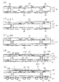
(下側パッケージの構造)
図1(b)に示すように、下側パッケージ1は、配線基板2と、その配線基板2にフリップチップ実装された半導体素子3と、それら配線基板2と半導体素子3との隙間を充填するように設けられたアンダーフィル樹脂4とを有している。
(Lower package structure)
As shown in FIG. 1B, the
配線基板2は、基板本体10と、最上層の配線パターン20、最下層の配線パターン30と、ソルダレジスト層40,41とを有している。
基板本体10は、コア基板11と、そのコア基板11に積層された複数の絶縁層12,13と、その複数の絶縁層12,13に形成された配線14,15及びビア16,17等を有している。基板本体10に設けられた配線14,15及びビア16,17は、配線パターン20及び配線パターン30を電気的に接続している。なお、配線14,15及びビア16,17の材料としては、例えば銅(Cu)を用いることができる。また、絶縁層12,13の材料としては、例えばエポキシ系樹脂やポリイミド樹脂などの絶縁樹脂を用いることができる。
The
The
配線パターン20は、基板本体10の実装面側(図中の上面側)に設けられている。この配線パターン20は、半導体素子3のバンプ3aと電気的に接続される半導体素子用パッド21、又は下側パッケージ1と上側パッケージ50(図3参照)との間を電気的に接続するための接続用パッド22を有している。半導体素子用パッド21は、平面視は図示を省略するが、半導体素子3のバンプ3aの配設形態に応じて、半導体素子3が実装される実装領域にマトリクス状に配列されている。この半導体素子用パッド21の平面形状は、例えば円形形状に形成されている。
The
一方、本実施形態の接続用パッド22は、図1(a)に示すように、半導体素子3の外周縁を囲む配置で二列に設けられている。この接続用パッド22の平面形状は、例えば直径240μm〜250μmの円形形状に形成されている。また、接続用パッド22のうち少なくとも2つの接続用パッド22Aの領域には、その接続用パッド22Aの平面形状よりも小さな面積を有する形状の認識マーク23が形成されている。この2つの接続用パッド22Aは、下側パッケージ1と上側パッケージ50(図3参照)とを電気的に接続する端子としての機能を有するとともに、認識マーク(上側パッケージを実装する際の位置合わせマークや製品識別マーク)としての機能も有している。このような認識マーク23の形成された接続用パッド22Aは、互いの離間距離を確保することにより認識マークとしての機能を高めることができるため、下側パッケージ1の平面対角線上に設けられている。認識マーク23の平面形状は、図2に示すように、接続用パッド22Aの平面形状とは異なる四角形状に形成されている。また、この認識マーク23は、接続用パッド22Aとして露出される配線パターン20の一部に凹部20Xが形成されることで形成されている。具体的には、接続用パッド22Aとして露出される配線パターン20の一部に、平面形状が四角形状の凹部20Xが形成されることで、その凹部20Xの側壁と接続用パッド22Aの上面との境界(段差部)が認識マーク23の輪郭として機能する。このような凹部20Xは、例えばエッチング加工(ハーフエッチング)やプレス加工などによって形成することができる。
On the other hand, the
なお、配線パターン20の材料としては、例えば銅を用いることができる。また、配線パターン20は、銅層の表面に所要のめっき(例えば、ニッケルめっきや金めっき等)を施して形成するようにしてもよい。
In addition, as a material of the
図1(b)に示すように、ソルダレジスト層40は、配線パターン20の一部を覆うように基板本体10の上面側に設けられている。ソルダレジスト層40の材料としては、例えばエポキシ系樹脂などの絶縁樹脂を用いることができる。このソルダレジスト層40には、半導体素子用パッド21又は接続用パッド22となる配線パターン20の一部を露出させるための複数の開口部40Xが形成されている。そして、アンダーフィル樹脂4が形成される前の状態において、この開口部40Xによって、配線パターン20の一部が半導体素子用パッド21又は接続用パッド22としてソルダレジスト層40から露出される。なお、開口部40Xの平面形状は、半導体素子用パッド21及び接続用パッド22が所望の形状となるように、本実施形態では円形形状に形成されている。
As shown in FIG. 1B, the
配線パターン30は、基板本体10の下面側に設けられている。この配線パターン30は、当該下側パッケージ1をマザーボード等の実装用基板に実装する際に使用されるはんだボールやリードピン等の外部接続端子32を配設するための外部接続用パッド31を有している。外部接続用パッド31は、基板本体10の下面側に形成されたソルダレジスト層41の開口部41Xから配線パターン30の一部が露出されることで形成されている。なお、配線パターン30の材料としては、例えば銅を用いることができる。また、配線パターン30は、銅層の表面に所要のめっき(例えば、ニッケルめっきや金めっき等)を施して形成するようにしてもよい。また、ソルダレジスト層41の材料としては、例えばエポキシ系樹脂などの絶縁樹脂を用いることができる。
The
半導体素子3は、このような構造を有する配線基板2にフリップチップ接合されている。すなわち、半導体素子3は、その回路形成面(図1(b)において下面)に配設されたバンプ3aを介して、配線基板2の半導体素子用パッド21と電気的に接続されている。
The
アンダーフィル樹脂4は、配線基板2の上面と半導体素子3の下面との隙間を充填するように設けられている。このアンダーフィル樹脂4は、バンプ3aと半導体素子用パッド21との接続部分の接続強度を向上させると共に、配線パターン20の腐食やエレクトロマイグレーションの発生を抑制し、配線パターン20の信頼性の低下を防ぐための樹脂である。なお、アンダーフィル樹脂4の材料としては、例えばエポキシ系樹脂などの絶縁樹脂を用いることができる。
The
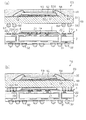
(上側パッケージの構造)
次に、上側パッケージ50の構造を説明する。
図3(b)に示すように、上側パッケージ50は、配線基板60と、その配線基板60にフリップチップ実装された第1の半導体素子52と、第1の半導体素子52の上に接着された第2の半導体素子53とを有している。また、上側パッケージ50は、第1の半導体素子52と配線基板60との隙間を充填するように設けられたアンダーフィル樹脂54と、第1の半導体素子52及び第2の半導体素子53等を封止する封止樹脂55とを有している。なお、図3(a)に示すように、第1の半導体素子52の平面形状は、第2の半導体素子53の平面形状よりも大きく形成されている。
(Upper package structure)
Next, the structure of the
As shown in FIG. 3B, the
図3(b)に示すように、配線基板60は、基板本体61と、基板本体61の上面に形成された半導体素子用パッド62及びボンディング用パッド63と、基板本体61の下面に形成された外部接続端子64とを有している。
As shown in FIG. 3B, the
基板本体61は、図示は省略するが、複数の絶縁層と、複数の絶縁層に形成されたビア及び配線等から構成されている。基板本体61に設けられたビア及び配線は、半導体素子用パッド62、ボンディング用パッド63及び外部接続端子64を電気的に接続している。基板本体61としては、例えばコアレス基板や、コア基板を有するコア付きビルドアップ基板等を用いることができる。
Although not shown, the
半導体素子用パッド62には、第1の半導体素子52のバンプ52aがフリップチップ接合されている。また、ボンディング用パッド63は、ボンディングワイヤ56を介して、第2の半導体素子53の上面に形成された電極パッド53Aと電気的に接続されている。これら半導体素子用パッド62及びボンディング用パッド63の材料としては、例えば銅を用いることができる。また、半導体素子用パッド62及びボンディング用パッド63は、銅層の表面に所要のめっき(例えば、ニッケルめっきや金めっき等)を施して形成するようにしてもよい。
外部接続端子64は、当該上側パッケージ50と下側パッケージ1(図1参照)との間を接続するための接続端子(例えば、はんだボールやリードピン)である。それぞれの外部接続端子64は、下側パッケージ1に配設されている接続用パッド22,22A(図1参照)の各々に対向するように設けられている。すなわち、図3(a)に示すように、外部接続端子64は、当該配線基板60の外周縁(外形)に沿ってペリフェラル状に二列に設けられている。
The
図3(b)に示すように、アンダーフィル樹脂54は、第1の半導体素子52のバンプ52aと半導体素子用パッド62との接続部分の接続強度を向上させるための樹脂であり、配線基板60の上面と第1の半導体素子52の下面との隙間を充填するように設けられている。なお、アンダーフィル樹脂54の材料としては、例えばエポキシ系樹脂などの絶縁樹脂を用いることができる。
As shown in FIG. 3B, the
封止樹脂55は、第1の半導体素子52、第2の半導体素子53、ボンディングワイヤ56及びボンディング用パッド63等を封止するように基板本体61の上面に設けられている。この封止樹脂55の材料としては、例えばエポキシ系樹脂を用いることができる。封止方法としては、例えばトランスファーモールド法を用いることができる。
The sealing
(半導体装置の構造)
次に、半導体装置70の構造について説明する。
図4に示すように、半導体装置70は、上述した下側パッケージ1と、その下側パッケージ1に積層接合された上側パッケージ50とを有している。
(Structure of semiconductor device)
Next, the structure of the
As shown in FIG. 4, the
下側パッケージ1の上面に形成された接続用パッド22,22Aには、上側パッケージ50の下面に形成された外部接続端子64が接合されている。これにより、下側パッケージ1と上側パッケージ50とが積層接合され、POP構造の半導体装置70が形成されている。
(半導体装置の作用)
次に、半導体装置70(特に、下側パッケージ1)の作用について説明する。
半導体装置70は、下側パッケージ1において、接続用パッド22のうち少なくとも2つの接続用パッド22Aに、その接続用パッド22Aよりも小さい平面形状を有する認識マーク23が形成されている。これにより、下側パッケージ1と上側パッケージ50との間を接続する端子として機能する接続用パッド22Aに認識マーク機能を持たせることができ、認識マークを形成するための専用領域を別途設ける必要がなくなる。また、接続用パッド22Aの領域内に認識マーク23を形成するようにしたため、接続用パッド22Aの平面形状を、その他の接続用パッド22の平面形状と同様の円形形状とすることができる。すなわち、認識マーク機能を持つ接続用パッド22Aの平面形状を、配線の高密度化に対応可能な形状(例えば、円形形状)に形成することができる。
(Operation of semiconductor device)
Next, the operation of the semiconductor device 70 (particularly the lower package 1) will be described.
In the
(半導体装置の製造方法)
次に、半導体装置70の製造方法について説明する。
まず、下側パッケージ1の製造方法について説明する。図5及び図6に示す下側パッケージ1の製造方法では、図5(a)に示すコア基板11を用いる。なお、このコア基板11は、例えば銅張積層板(Copper Clad Laminated:CCL)にスルーホール10Xを形成し、スルーホール10Xの側面にめっきを施すことで両面を導通させた後、サブトラクティブ法により配線14,15を形成することによって製造される。
(Method for manufacturing semiconductor device)
Next, a method for manufacturing the
First, a method for manufacturing the
このコア基板11の両面側に、図5(b)に示すように絶縁層12,13を形成する。次に、図5(c)に示すように、配線14,15の上面の一部が露出されるように、絶縁層12,13の所定箇所にそれぞれ開口部12X,13Xを形成する。この開口部12X,13Xは、例えばレーザ加工によって形成される。
Insulating
続いて、デスミア処理後、図5(d)に示すように、絶縁層12及び配線14を覆うようにシード層S1を形成するとともに、絶縁層13及び配線15を覆うようにシード層S2を形成する。これらシード層S1,S2は、無電解銅めっき又はスパッタリングによって形成される。
Subsequently, after the desmear process, as shown in FIG. 5D, the seed layer S1 is formed so as to cover the insulating
次に、図5(e)に示すように、例えばセミアディティブ法により配線パターン20,30及びビア16,17を形成する。すなわち、シード層S1上に配線パターン20の形状に対応した開口パターン80Xを有するドライフィルムレジスト(DFR)80をフォトリソグラフィ法により形成し、上記シード層S1を給電層とする電解めっきによって配線パターン20及びビア16を形成する。なお、配線パターン30及びビア17も、上記配線パターン20及びビア16と同様に形成される。
Next, as shown in FIG. 5E, the
このように配線パターン20,30及びビア16,17が形成されると、図6(a)に示すように、DFR80及び不要なシード層S1,S2が除去される。
次に、図6(b)に示すように、絶縁層12の上面に、認識マーク23(図2参照)の形状に対応した開口部81Xを有するレジスト層81を形成する。例えば配線パターン20及び絶縁層12を覆うようにレジスト層81を形成後、フォトリソグラフィ法によりレジスト層81を露光・現像して配線パターン20の上面の一部を露出させる開口部81Xを形成する。このときの開口部81Xは、平面形状が四角形となる。なお、レジスト層81の材料としては、所望の解像性があり、耐エッチング性がある材料であれば、特に限定されない。
When the
Next, as illustrated in FIG. 6B, a resist
次に、図6(c)に示すように、レジスト層81をエッチングマスクとして、開口部81Xから露出している配線パターン20の部分にハーフエッチングを施し、当該部分を所要の深さまで除去して薄くする。これにより、開口部81Xから露出している配線パターン20に凹部20Xが形成される。この工程で使用されるエッチング液は、配線パターン20の材料に応じて適宜選択することができる。例えば配線パターン20として銅を用いる場合には、エッチング液として塩化第二鉄水溶液を用いることができる。なお、このようなエッチング加工(ハーフエッチング)により凹部20Xを形成することも可能であるが、例えばプレス加工により凹部20Xを形成することもできる。
Next, as shown in FIG. 6C, using the resist
続いて、上記凹部20Xの形成後に、レジスト層81を例えばアッシングにより除去する。
次いで、図6(d)に示すように、絶縁層12上に、配線パターン20の上面の一部を露出させる開口部40Xを有するソルダレジスト層40を形成する。例えば配線パターン20及び絶縁層12を覆うようにソルダレジスト層40を形成後、フォトリソグラフィ法によりソルダレジスト層40を露光・現像して配線パターン20の上面の一部を露出させる開口部40Xを形成する。ここで、開口部40Xは、上記レジスト層81の開口部81Xよりも平面形状が大きくなるように形成される。そして、この開口部40Xによって、配線パターン20の一部が半導体素子用パッド21又は接続用パッド22,22Aとしてソルダレジスト層40から露出される。さらに、このとき、接続用パッド22Aでは、上記凹部20Xの全てが開口部40Xから露出され、その凹部20Xによって認識マーク23が形成される。
Subsequently, after the formation of the
Next, as illustrated in FIG. 6D, a solder resist
また、絶縁層13の下面に、配線パターン30の下面の一部を露出させる開口部41Xを有するソルダレジスト層41を形成する。例えば配線パターン30及び絶縁層13を覆うようにソルダレジスト層41を形成後、フォトリソグラフィ法によりソルダレジスト層41を露光・現像して配線パターン30の下面の一部を露出させる開口部41Xを形成する。この開口部41Xによって、配線パターン30の一部が外部接続用パッド31としてソルダレジスト層41から露出される。
Further, a solder resist
次に、図6(e)に示すように、外部接続用パッド31上に、外部接続端子32を形成する。例えば外部接続用パッド31上に、適宜フラックスを塗布した後、外部接続端子32(ここでは、はんだボール)を搭載し、240〜260℃程度の温度でリフローして固定する。その後、表面を洗浄してフラックスを除去する。
Next, as shown in FIG. 6E,
続いて、このように製造された配線基板2に半導体素子3を実装する。具体的には、配線基板2の半導体素子用パッド21上に、半導体素子3のバンプ3aをフリップチップ接合する。続いて、フリップチップ接合された配線基板2と半導体素子3との間に、アンダーフィル樹脂4を充填し、そのアンダーフィル樹脂4を硬化する。以上の製造工程により、本実施形態の下側パッケージ1を製造することができる。
Subsequently, the
次に、図7(a)に示すように、上側パッケージ50を用意する。ここでは、図示を省略して詳細な説明を割愛するが、上側パッケージ50は例えば以下のような方法で製造される。すなわち、半導体素子用パッド62、ボンディング用パッド63及び外部接続端子64を有する配線基板60を形成し、その配線基板60の上面に形成された半導体素子用パッド62に第1の半導体素子52のバンプ52aをフリップチップ接合する。続いて、配線基板60と第1の半導体素子52との間にアンダーフィル樹脂54を形成した後、第1の半導体素子52の上に第2の半導体素子53を接着剤により接着する。次いで、第2の半導体素子53の上面に形成された電極パッド53Aと配線基板60の上面に形成されたボンディング用パッド63との間をボンディングワイヤ56によりワイヤボンディング接続した後、半導体素子52,53及びボンディングワイヤ56等を封止樹脂55で樹脂封止する。
Next, as shown in FIG. 7A, an
次に、下側パッケージ1に上側パッケージ50を積層接合(実装)する。以下にこの方法について詳述する。
まず、下側パッケージ1がキャリア(図示略)に収納され、その収納された下側パッケージ1の表面(上面)が、固定点に配設されたカメラ(図示略)により撮影される。このとき、カメラにより撮影された撮影画像が画像処理され、下側パッケージ1の接続用パッド22Aに形成された認識マーク23の位置が検出され、2つの認識マーク23の配置位置から下側パッケージ1の品種が識別される。この識別によって下側パッケージ1が所望の品種(製品)でないと判別された場合には、その下側パッケージ1に上側パッケージ50を搭載しないようにする。また、必要に応じてエラーメッセージを発する。
Next, the
First, the
一方、下側パッケージ1が所望の品種(製品)であると判別された場合には、上記検出された認識マーク23の位置に基づいて、下側パッケージ1の位置が認識される。そして、その認識された下側パッケージ1の位置に基づいて、図7(a)に示すように、下側パッケージ1の接続用パッド22,22Aに、上側パッケージ50の外部接続端子64を位置合わせする。このとき、上側パッケージ50の外部接続端子64には図示しないフラックスが転写されている。
On the other hand, when it is determined that the
次に、キャリアにセットされている下側パッケージ1に位置合わせして上側パッケージ50が載置されると、キャリアがリフロー炉(図示略)に搬送される。そして、このリフロー炉内では外部接続端子64(はんだボール)がリフローされ、接続用パッド22,22A部分で下側パッケージ1と上側パッケージ50とが接合される。これにより、図7(b)に示すようなPOP構造の半導体装置70が製造される。
Next, when the
以上説明した本実施形態によれば、以下の効果を奏することができる。
(1)下側パッケージ1において、接続用パッド22のうち少なくとも2つの接続用パッド22Aに、その接続用パッド22Aよりも小さい平面形状を有する認識マーク23を形成するようにした。これにより、接続用パッド22Aに認識マーク機能を持たせることができ、認識マークを形成するための専用領域を別途設ける必要がなくなる。また、接続用パッド22Aの領域内に認識マーク23を形成するようにしたため、接続用パッド22Aの平面形状を、その他の接続用パッド22の平面形状と同様の円形形状とすることができる。すなわち、認識マーク機能を持つ接続用パッド22Aの平面形状を、配線の高密度化に対応可能な形状(例えば、円形形状)に維持することができる。
According to this embodiment described above, the following effects can be obtained.
(1) In the
(2)接続用パッド22,22Aよりも小さい平面形状となるように、つまり接続用パッド22,22Aと異なる形状になるように認識マーク23を形成するようにした。このため、カメラ等によって認識マーク23を検出する際に、認識マーク23と、接続用パッド22,22Aとを容易に判別することができ、認識マーク23の位置を容易に検出(認識)することができる。
(2) The
(3)配線パターン20に形成された凹部20Xによって認識マーク23が形成される、つまり認識マーク23の輪郭(外形)が段差部によって形成される。これにより、カメラ等によって認識マーク23を検出する際に、認識マーク23と接続用パッド22Aの上面とのコントラストが得やすくなり、認識マーク23の輪郭を認識し易くなるため、認識マーク23の認識性を向上させることができる。したがって、下側パッケージ1に上側パッケージ50を搭載する際において、下側パッケージ1の位置認識の精度を向上させることができる。
(3) The
さらに、接続用パッド22Aの大部分に認識マーク23が形成される場合であっても、その認識マーク23は配線パターン20によって形成されているため、上側パッケージ50の外部接続端子64と接合される配線パターン20の表面積を、接続用パッド22と同様に確保することができる。これにより、接続用パッド22Aにおいて、外部接続端子64との接合強度が低下するといった問題の発生を抑制することができる。
Further, even when the
(他の実施形態)
なお、上記実施形態は、これを適宜変更した以下の態様にて実施することもできる。
・上記実施形態では、認識マーク23の平面形状を四角形状にしたが、これに限定されない。例えば図8に示すように、認識マーク23の平面形状を十字状(図8(a)参照)や三角形状(図8(b)参照)となるように形成してもよい。また、認識マーク23の平面形状を円形形状(図8(c)参照)となるように形成してもよい。このとき、認識マーク23と接続用パッド22,22Aとの平面形状が共に円形形状になるため、それら認識マーク23と接続用パッド22,22Aとを判別可能な面積差となるように、認識マーク23を接続用パッド22,22Aよりも小さく形成する。以上のように、接続用パッド22,22Aと判別することのできる形状であれば、認識マーク23の形状は特に限定されず、他にも例えば認識マーク23の平面形状を×字形状や−字形状となるように形成することができる。
(Other embodiments)
In addition, the said embodiment can also be implemented in the following aspects which changed this suitably.
In the above embodiment, the planar shape of the
・上記実施形態では、接続用パッド22Aとして露出される配線パターン20の一部に形成された凹部20Xによって認識マーク23を形成するようにした。これに限らず、例えば接続用パッド22Aとして露出される配線パターン20の一部に凸部を形成し、その凸部によって認識マーク23を形成するようにしてもよい。
In the above embodiment, the
・上記実施形態では、接続用パッド22Aとして露出される配線パターン20の一部を薄化して認識マーク23を形成するようにした。これに限らず、例えば図8(d)に示すように、接続用パッド22Aとして露出される配線パターン20の一部を除去し、その配線パターン20の下層の絶縁層12を露出させて認識マーク23を形成するようにしてもよい。この場合には、認識マーク23の境界部分が、絶縁層12と配線パターン20という材質の異なる部材によって形成されるため、カメラ等によって認識マーク23を検出する際に、認識マーク23の輪郭を認識し易くなる。これにより、認識マーク23の認識性を向上させることができ、ひいては下側パッケージ1に上側パッケージ50を搭載する際における下側パッケージ1の位置認識の精度を向上させることができる。但し、この場合には、上側パッケージ50の外部接続端子64との接合強度を考慮して、配線パターン20を除去する領域を極力小さくすることが好ましい。
In the above embodiment, the
なお、図8(d)では、接続用パッド22Aとして露出される配線パターン20のうち、平面形状が直線形状の4つの小領域23Aで配線パターン20が除去されている。また、これら4つの小領域23Aは、接続用パッド22Aの領域において平面視で略四角形を構成する位置に設けられている。そして、これら4つの小領域23Aを合わせた形状が認識マーク23として機能する。
In FIG. 8D, among the
・上記実施形態における接続用パッド22A、つまり認識マーク23の形成された接続用パッド22Aの数及び配置位置に特に限定されない。すなわち、接続用パッド22Aを3つ以上設けるようにしてもよい。また、上記実施形態では、接続用パッド22Aを下側パッケージ1の平面対角線上に設けるようにしたが、例えば下側パッケージにおいて平面視で三角形を構成する位置に接続用パッド22Aを設けるようにしてもよい。
The number of
・上記実施形態の下側パッケージ1の配線基板2において、配線パターン20,30の下層の構造については特に限定されない。例えばコア基板11の構造及び材質は特に限定されない。また、コア基板11上に形成される下層配線(例えば、配線14,15)とそれを覆う絶縁層(例えば、絶縁層12,13)の層数についても特に限定されない。あるいは、基板本体10として、コアレス基板を用いるようにしてもよい。
In the
・上記実施形態では、下側パッケージ1の配線基板2に外部接続端子32を形成するようにしたが、この外部接続端子32を省略することもできる。すなわち、必要なときに外部接続端子32等を形成できるように配線パターン30の一部が外部接続用パッド31としてソルダレジスト層41から露出された状態のままにしておいてもよい。
In the above embodiment, the
・上記実施形態の上側パッケージ50においては、半導体素子の積層構造としてフリップチップ接続とワイヤボンディング接続を併用した構造を採用した。これに限らず、第1の半導体素子52の上に第2の半導体素子53を積層する際に、両方の半導体素子52,53を共にワイヤボンディング接続により接続する形態や、両方の半導体素子52,53を共にフリップチップ接続により接続した積層形態を採用してもよい。また、配線基板60に実装する半導体素子は1つであってもよい。
In the
1 下側パッケージ(半導体パッケージ)
2 配線基板
12 絶縁層
20 配線パターン
20X 凹部
22 接続用パッド
22A 接続用パッド
23 認識マーク
50 上側パッケージ(搭載用部品)
64 外部接続端子
70 半導体装置
1 Lower package (semiconductor package)
2 Wiring
64
Claims (3)
前記配線パターンを被覆し、前記配線パターンの一部を接続用パッドとして露出する開口部を有するソルダレジスト層と、
半導体パッケージに搭載される搭載用部品の接続端子と電気的に接続される複数の前記接続用パッドと、
前記接続用パッドのうち少なくとも2つの第1接続用パッドの領域内に形成され、前記第1接続用パッドよりも小さい平面形状を有する認識マークと、を有し、
前記第1接続用パッドとして露出される前記配線パターンの一部に凹部又は凸部が形成されることで前記認識マークが形成されていることを特徴とする半導体パッケージ。 The uppermost wiring pattern,
A solder resist layer that covers the wiring pattern and has an opening that exposes a part of the wiring pattern as a connection pad;
A plurality of the connecting pad connected terminals electrically connected to mounting components mounted on the semiconductor package,
A recognition mark formed in a region of at least two first connection pads of the connection pads and having a smaller planar shape than the first connection pads;
Semiconductor package, characterized in that said recognition mark by concave or convex portions are formed on a part of the wiring pattern to be exposed is formed as the first connection pad.
前記認識マークの平面形状は、前記第1接続用パッドと異なる形状であることを特徴とする請求項1又は2に記載の半導体パッケージ。 The planar shape of the first connection pad is a circular shape,
The planar shape of the recognition marks, the semiconductor package according to claim 1 or 2, characterized in that the first connection pad is shaped differently.
Priority Applications (2)
| Application Number | Priority Date | Filing Date | Title |
|---|---|---|---|
| JP2011129230A JP5795196B2 (en) | 2011-06-09 | 2011-06-09 | Semiconductor package |
| US13/483,464 US9406620B2 (en) | 2011-06-09 | 2012-05-30 | Semiconductor package |
Applications Claiming Priority (1)
| Application Number | Priority Date | Filing Date | Title |
|---|---|---|---|
| JP2011129230A JP5795196B2 (en) | 2011-06-09 | 2011-06-09 | Semiconductor package |
Publications (3)
| Publication Number | Publication Date |
|---|---|
| JP2012256741A JP2012256741A (en) | 2012-12-27 |
| JP2012256741A5 JP2012256741A5 (en) | 2014-06-19 |
| JP5795196B2 true JP5795196B2 (en) | 2015-10-14 |
Family
ID=47292492
Family Applications (1)
| Application Number | Title | Priority Date | Filing Date |
|---|---|---|---|
| JP2011129230A Active JP5795196B2 (en) | 2011-06-09 | 2011-06-09 | Semiconductor package |
Country Status (2)
| Country | Link |
|---|---|
| US (1) | US9406620B2 (en) |
| JP (1) | JP5795196B2 (en) |
Families Citing this family (14)
| Publication number | Priority date | Publication date | Assignee | Title |
|---|---|---|---|---|
| US11131431B2 (en) | 2014-09-28 | 2021-09-28 | Jiaxing Super Lighting Electric Appliance Co., Ltd | LED tube lamp |
| US9343386B2 (en) * | 2013-06-19 | 2016-05-17 | Taiwan Semiconductor Manufacturing Company, Ltd. | Alignment in the packaging of integrated circuits |
| CN103390563B (en) * | 2013-08-06 | 2016-03-30 | 江苏长电科技股份有限公司 | Erosion flip-chip of being first honored as a queen three-dimensional systematic metal circuit board structure &processes method |
| CN103489792B (en) * | 2013-08-06 | 2016-02-03 | 江苏长电科技股份有限公司 | First be honored as a queen and lose three-dimensional systematic flip chip encapsulation structure and process |
| US10560989B2 (en) | 2014-09-28 | 2020-02-11 | Jiaxing Super Lighting Electric Appliance Co., Ltd | LED tube lamp |
| WO2016045630A1 (en) | 2014-09-28 | 2016-03-31 | Jiaxing Super Lighting Electric Appliance Co., Ltd | Led tube lamp |
| US10514134B2 (en) | 2014-12-05 | 2019-12-24 | Jiaxing Super Lighting Electric Appliance Co., Ltd | LED tube lamp |
| US11028973B2 (en) | 2015-03-10 | 2021-06-08 | Jiaxing Super Lighting Electric Appliance Co., Ltd. | Led tube lamp |
| US9897265B2 (en) | 2015-03-10 | 2018-02-20 | Jiaxing Super Lighting Electric Appliance Co., Ltd. | LED tube lamp having LED light strip |
| US11519565B2 (en) | 2015-03-10 | 2022-12-06 | Jiaxing Super Lighting Electric Appliance Co., Ltd | LED lamp and its power source module |
| US11035526B2 (en) | 2015-12-09 | 2021-06-15 | Jiaxing Super Lighting Electric Appliance Co., Ltd. | LED tube lamp |
| CN110475429A (en) * | 2018-05-10 | 2019-11-19 | Oppo广东移动通信有限公司 | Semiconductor element and chip mounter, patch system |
| KR102554017B1 (en) | 2018-10-02 | 2023-07-11 | 삼성전자주식회사 | Semiconductor package |
| JP2022175499A (en) * | 2021-05-13 | 2022-11-25 | 新光電気工業株式会社 | Wiring substrate, semiconductor device, and method for manufacturing wiring substrate |
Family Cites Families (7)
| Publication number | Priority date | Publication date | Assignee | Title |
|---|---|---|---|---|
| WO2002082540A1 (en) | 2001-03-30 | 2002-10-17 | Fujitsu Limited | Semiconductor device, method of manufacture thereof, and semiconductor substrate |
| JP2003318359A (en) * | 2002-04-25 | 2003-11-07 | Optrex Corp | Wiring board and mounting wiring board |
| JP3989869B2 (en) * | 2003-04-14 | 2007-10-10 | 沖電気工業株式会社 | Semiconductor device and manufacturing method thereof |
| US8072076B2 (en) * | 2006-10-11 | 2011-12-06 | Taiwan Semiconductor Manufacturing Co., Ltd. | Bond pad structures and integrated circuit chip having the same |
| JP5049573B2 (en) * | 2006-12-12 | 2012-10-17 | 新光電気工業株式会社 | Semiconductor device |
| KR100809726B1 (en) * | 2007-05-14 | 2008-03-06 | 삼성전자주식회사 | Align mark, semiconductor chip having the align mark, semiconductor package having the chip, and methods of fabricating the chip and the package |
| JP5232460B2 (en) | 2007-12-12 | 2013-07-10 | 新光電気工業株式会社 | Semiconductor package |
-
2011
- 2011-06-09 JP JP2011129230A patent/JP5795196B2/en active Active
-
2012
- 2012-05-30 US US13/483,464 patent/US9406620B2/en active Active
Also Published As
| Publication number | Publication date |
|---|---|
| US9406620B2 (en) | 2016-08-02 |
| JP2012256741A (en) | 2012-12-27 |
| US20120313265A1 (en) | 2012-12-13 |
Similar Documents
| Publication | Publication Date | Title |
|---|---|---|
| JP5795196B2 (en) | Semiconductor package | |
| JP6076653B2 (en) | Electronic component built-in substrate and manufacturing method of electronic component built-in substrate | |
| JP5851211B2 (en) | Semiconductor package, semiconductor package manufacturing method, and semiconductor device | |
| JP5460388B2 (en) | Semiconductor device and manufacturing method thereof | |
| TWI483363B (en) | Package substrate, package structure and method for manufacturing package structure | |
| JP2013162128A (en) | Package-on-package-type semiconductor package and method of fabricating the same | |
| US20060091524A1 (en) | Semiconductor module, process for producing the same, and film interposer | |
| US20140061951A1 (en) | Package on package structure and method for manufacturing same | |
| US9204546B2 (en) | Circuit board and manufacturing method thereof | |
| JP6352644B2 (en) | Wiring substrate and semiconductor package manufacturing method | |
| JP2008218979A (en) | Electronic packaging and manufacturing method thereof | |
| JP2010287870A (en) | Printed circuit board, semiconductor device including the same, and method of manufacturing the same | |
| JP2011014944A (en) | Method of manufacturing electronic parts packaging structure | |
| JP2017174849A (en) | Semiconductor device and semiconductor device manufacturing method | |
| KR20160086181A (en) | Printed circuit board, package and method of manufacturing the same | |
| TWI506758B (en) | Package on package structure and method for manufacturing same | |
| CN113496983A (en) | Semiconductor package carrier, method for fabricating the same and semiconductor package process | |
| JP6713289B2 (en) | Semiconductor device and method of manufacturing semiconductor device | |
| KR102633431B1 (en) | Semiconductor device and manufacturing method thereof | |
| KR20220077751A (en) | Printed circuit boardand and electronic component package | |
| KR101340348B1 (en) | Embedded chip package board using mask pattern and method for manufacturing the same | |
| TWI720735B (en) | Package structure and manufacturing method thereof | |
| US11908810B2 (en) | Hybrid semiconductor device and electronic device | |
| JP4955997B2 (en) | Circuit module and method of manufacturing circuit module | |
| US20190013263A1 (en) | Wiring board and semiconductor package |
Legal Events
| Date | Code | Title | Description |
|---|---|---|---|
| A521 | Written amendment |
Free format text: JAPANESE INTERMEDIATE CODE: A523 Effective date: 20140423 |
|
| A621 | Written request for application examination |
Free format text: JAPANESE INTERMEDIATE CODE: A621 Effective date: 20140423 |
|
| A977 | Report on retrieval |
Free format text: JAPANESE INTERMEDIATE CODE: A971007 Effective date: 20140918 |
|
| A131 | Notification of reasons for refusal |
Free format text: JAPANESE INTERMEDIATE CODE: A131 Effective date: 20140924 |
|
| A521 | Written amendment |
Free format text: JAPANESE INTERMEDIATE CODE: A523 Effective date: 20141112 |
|
| A131 | Notification of reasons for refusal |
Free format text: JAPANESE INTERMEDIATE CODE: A131 Effective date: 20150512 |
|
| A521 | Written amendment |
Free format text: JAPANESE INTERMEDIATE CODE: A523 Effective date: 20150708 |
|
| TRDD | Decision of grant or rejection written | ||
| A01 | Written decision to grant a patent or to grant a registration (utility model) |
Free format text: JAPANESE INTERMEDIATE CODE: A01 Effective date: 20150804 |
|
| A61 | First payment of annual fees (during grant procedure) |
Free format text: JAPANESE INTERMEDIATE CODE: A61 Effective date: 20150812 |
|
| R150 | Certificate of patent or registration of utility model |
Ref document number: 5795196 Country of ref document: JP Free format text: JAPANESE INTERMEDIATE CODE: R150 |