JP5780120B2 - Power supply system, image forming apparatus equipped with the power supply system, and small-capacity power supply circuit - Google Patents
Power supply system, image forming apparatus equipped with the power supply system, and small-capacity power supply circuit Download PDFInfo
- Publication number
- JP5780120B2 JP5780120B2 JP2011241367A JP2011241367A JP5780120B2 JP 5780120 B2 JP5780120 B2 JP 5780120B2 JP 2011241367 A JP2011241367 A JP 2011241367A JP 2011241367 A JP2011241367 A JP 2011241367A JP 5780120 B2 JP5780120 B2 JP 5780120B2
- Authority
- JP
- Japan
- Prior art keywords
- power supply
- electrode
- voltage
- capacitor
- zero
- Prior art date
- Legal status (The legal status is an assumption and is not a legal conclusion. Google has not performed a legal analysis and makes no representation as to the accuracy of the status listed.)
- Active
Links
Images


Classifications
-
- G—PHYSICS
- G03—PHOTOGRAPHY; CINEMATOGRAPHY; ANALOGOUS TECHNIQUES USING WAVES OTHER THAN OPTICAL WAVES; ELECTROGRAPHY; HOLOGRAPHY
- G03G—ELECTROGRAPHY; ELECTROPHOTOGRAPHY; MAGNETOGRAPHY
- G03G15/00—Apparatus for electrographic processes using a charge pattern
- G03G15/50—Machine control of apparatus for electrographic processes using a charge pattern, e.g. regulating differents parts of the machine, multimode copiers, microprocessor control
- G03G15/5004—Power supply control, e.g. power-saving mode, automatic power turn-off
-
- G—PHYSICS
- G03—PHOTOGRAPHY; CINEMATOGRAPHY; ANALOGOUS TECHNIQUES USING WAVES OTHER THAN OPTICAL WAVES; ELECTROGRAPHY; HOLOGRAPHY
- G03G—ELECTROGRAPHY; ELECTROPHOTOGRAPHY; MAGNETOGRAPHY
- G03G15/00—Apparatus for electrographic processes using a charge pattern
- G03G15/80—Details relating to power supplies, circuits boards, electrical connections
-
- H—ELECTRICITY
- H02—GENERATION; CONVERSION OR DISTRIBUTION OF ELECTRIC POWER
- H02M—APPARATUS FOR CONVERSION BETWEEN AC AND AC, BETWEEN AC AND DC, OR BETWEEN DC AND DC, AND FOR USE WITH MAINS OR SIMILAR POWER SUPPLY SYSTEMS; CONVERSION OF DC OR AC INPUT POWER INTO SURGE OUTPUT POWER; CONTROL OR REGULATION THEREOF
- H02M7/00—Conversion of ac power input into dc power output; Conversion of dc power input into ac power output
- H02M7/02—Conversion of ac power input into dc power output without possibility of reversal
- H02M7/04—Conversion of ac power input into dc power output without possibility of reversal by static converters
- H02M7/06—Conversion of ac power input into dc power output without possibility of reversal by static converters using discharge tubes without control electrode or semiconductor devices without control electrode
-
- G—PHYSICS
- G01—MEASURING; TESTING
- G01R—MEASURING ELECTRIC VARIABLES; MEASURING MAGNETIC VARIABLES
- G01R19/00—Arrangements for measuring currents or voltages or for indicating presence or sign thereof
- G01R19/175—Indicating the instants of passage of current or voltage through a given value, e.g. passage through zero
-
- G—PHYSICS
- G06—COMPUTING; CALCULATING OR COUNTING
- G06F—ELECTRIC DIGITAL DATA PROCESSING
- G06F1/00—Details not covered by groups G06F3/00 - G06F13/00 and G06F21/00
- G06F1/26—Power supply means, e.g. regulation thereof
- G06F1/32—Means for saving power
- G06F1/3203—Power management, i.e. event-based initiation of a power-saving mode
- G06F1/3234—Power saving characterised by the action undertaken
- G06F1/325—Power saving in peripheral device
- G06F1/3284—Power saving in printer
-
- H—ELECTRICITY
- H02—GENERATION; CONVERSION OR DISTRIBUTION OF ELECTRIC POWER
- H02M—APPARATUS FOR CONVERSION BETWEEN AC AND AC, BETWEEN AC AND DC, OR BETWEEN DC AND DC, AND FOR USE WITH MAINS OR SIMILAR POWER SUPPLY SYSTEMS; CONVERSION OF DC OR AC INPUT POWER INTO SURGE OUTPUT POWER; CONTROL OR REGULATION THEREOF
- H02M1/00—Details of apparatus for conversion
- H02M1/0003—Details of control, feedback or regulation circuits
- H02M1/0006—Arrangements for supplying an adequate voltage to the control circuit of converters
-
- H—ELECTRICITY
- H02—GENERATION; CONVERSION OR DISTRIBUTION OF ELECTRIC POWER
- H02M—APPARATUS FOR CONVERSION BETWEEN AC AND AC, BETWEEN AC AND DC, OR BETWEEN DC AND DC, AND FOR USE WITH MAINS OR SIMILAR POWER SUPPLY SYSTEMS; CONVERSION OF DC OR AC INPUT POWER INTO SURGE OUTPUT POWER; CONTROL OR REGULATION THEREOF
- H02M1/00—Details of apparatus for conversion
- H02M1/0003—Details of control, feedback or regulation circuits
- H02M1/0032—Control circuits allowing low power mode operation, e.g. in standby mode
-
- H—ELECTRICITY
- H02—GENERATION; CONVERSION OR DISTRIBUTION OF ELECTRIC POWER
- H02M—APPARATUS FOR CONVERSION BETWEEN AC AND AC, BETWEEN AC AND DC, OR BETWEEN DC AND DC, AND FOR USE WITH MAINS OR SIMILAR POWER SUPPLY SYSTEMS; CONVERSION OF DC OR AC INPUT POWER INTO SURGE OUTPUT POWER; CONTROL OR REGULATION THEREOF
- H02M1/00—Details of apparatus for conversion
- H02M1/0048—Circuits or arrangements for reducing losses
-
- H—ELECTRICITY
- H02—GENERATION; CONVERSION OR DISTRIBUTION OF ELECTRIC POWER
- H02M—APPARATUS FOR CONVERSION BETWEEN AC AND AC, BETWEEN AC AND DC, OR BETWEEN DC AND DC, AND FOR USE WITH MAINS OR SIMILAR POWER SUPPLY SYSTEMS; CONVERSION OF DC OR AC INPUT POWER INTO SURGE OUTPUT POWER; CONTROL OR REGULATION THEREOF
- H02M1/00—Details of apparatus for conversion
- H02M1/0067—Converter structures employing plural converter units, other than for parallel operation of the units on a single load
- H02M1/007—Plural converter units in cascade
-
- H—ELECTRICITY
- H02—GENERATION; CONVERSION OR DISTRIBUTION OF ELECTRIC POWER
- H02M—APPARATUS FOR CONVERSION BETWEEN AC AND AC, BETWEEN AC AND DC, OR BETWEEN DC AND DC, AND FOR USE WITH MAINS OR SIMILAR POWER SUPPLY SYSTEMS; CONVERSION OF DC OR AC INPUT POWER INTO SURGE OUTPUT POWER; CONTROL OR REGULATION THEREOF
- H02M7/00—Conversion of ac power input into dc power output; Conversion of dc power input into ac power output
- H02M7/02—Conversion of ac power input into dc power output without possibility of reversal
- H02M7/04—Conversion of ac power input into dc power output without possibility of reversal by static converters
- H02M7/05—Capacitor coupled rectifiers
-
- Y—GENERAL TAGGING OF NEW TECHNOLOGICAL DEVELOPMENTS; GENERAL TAGGING OF CROSS-SECTIONAL TECHNOLOGIES SPANNING OVER SEVERAL SECTIONS OF THE IPC; TECHNICAL SUBJECTS COVERED BY FORMER USPC CROSS-REFERENCE ART COLLECTIONS [XRACs] AND DIGESTS
- Y02—TECHNOLOGIES OR APPLICATIONS FOR MITIGATION OR ADAPTATION AGAINST CLIMATE CHANGE
- Y02B—CLIMATE CHANGE MITIGATION TECHNOLOGIES RELATED TO BUILDINGS, e.g. HOUSING, HOUSE APPLIANCES OR RELATED END-USER APPLICATIONS
- Y02B70/00—Technologies for an efficient end-user side electric power management and consumption
- Y02B70/10—Technologies improving the efficiency by using switched-mode power supplies [SMPS], i.e. efficient power electronics conversion e.g. power factor correction or reduction of losses in power supplies or efficient standby modes
Description
本発明は、電源システム、同電源システムを備えた画像形成装置および小容量電源回路に関し、詳しくは、交流電圧のゼロクロス点を検出する技術に関する。 The present invention relates to a power supply system, an image forming apparatus including the power supply system, and a small-capacity power supply circuit, and more particularly to a technique for detecting a zero-cross point of an AC voltage.
従来、交流電圧のゼロクロス点(ゼロクロスタイミング)を検出する技術として、例えば、特許文献1に記載されたものが知られている。その従来技術文献においては、フォトカプラを利用して交流電圧のゼロクロス点を検知する技術が開示されている。
Conventionally, for example, a technique described in
しかしながら、上記従来技術文献のように、フォトカプラを利用したゼロクロス点の検知方法では、好適にゼロクロス点を検知できるものの、フォトカプラのフォトダイオードによる消費電力量が無視できる程度に低くはなかった。そのため、より省電力化が可能なゼロクロス点を検知する技術が切望されていた。
本発明は、より省電力化の可能な、ゼロクロス点の検知技術を提供するものである。
However, although the zero cross point detection method using the photocoupler as described in the above prior art document can detect the zero cross point suitably, the power consumption by the photodiode of the photocoupler is not low enough to be ignored. For this reason, a technique for detecting a zero-cross point capable of further saving power has been desired.
The present invention provides a zero-cross point detection technique that can further save power.
本明細書によって開示される電源システムは、交流電源の交流電圧を整流平滑化し、発振を行う通常モードにおいて所定の直流電圧を生成するスイッチング電源と、前記スイッチング電源を、前記通常モードと、前記スイッチング電源の発振を停止させる省電力モードとに切り換え制御する制御装置と、前記省電力モードにおいて前記制御装置に電力を供給する小容量電源回路であって、第1電極および第2電極を有し、当該第1電極が前記交流電源の一端に接続される第1コンデンサと、第1電極および第2電極を有し、当該第1電極が前記交流電源の他端に接続される第2コンデンサと、前記第1コンデンサの前記第2電極と前記第2コンデンサの前記第2電極との間に電気的に接続され、両コンデンサに印加される交流電圧を整流する整流回路とを含む小容量電源回路とを備え、前記小容量電源回路は、前記整流回路の後段の電流経路に接続され、前記電流経路に流れる整流電流に基づいて前記交流電源のゼロクロス点を検出するゼロクロス検出回路を含む。 The power supply system disclosed in the present specification includes a switching power supply that generates a predetermined DC voltage in a normal mode that rectifies and smoothes an AC voltage of an AC power supply and performs oscillation, the switching power supply, the normal mode, and the switching power supply. A control device that controls switching to a power saving mode for stopping oscillation of a power supply, and a small-capacity power supply circuit that supplies power to the control device in the power saving mode, and includes a first electrode and a second electrode, A first capacitor having the first electrode connected to one end of the AC power source, a first capacitor having a first electrode and a second electrode, and the second electrode having the first electrode connected to the other end of the AC power source; Electrically connected between the second electrode of the first capacitor and the second electrode of the second capacitor to rectify the AC voltage applied to both capacitors A small-capacity power supply circuit including a current circuit, and the small-capacity power supply circuit is connected to a current path downstream of the rectifier circuit and detects a zero cross point of the AC power supply based on a rectified current flowing in the current path Including a zero-cross detection circuit.
上記電源システムにおいて、前記ゼロクロス検出回路は、前記平滑コンデンサと基準電位配線とを結ぶ電流経路に接続されるようにしてもよい。 In the power supply system, the zero cross detection circuit may be connected to a current path connecting the smoothing capacitor and a reference potential wiring.
また、上記電源システムにおいて、前記整流回路に接続される専用電流経路をさらに備え、前記ゼロクロス検出回路は前記専用電流経路に接続されるようにしてもよい。
その場合、前記専用電流経路は、直列接続された二個の分圧抵抗によって構成されるとともに、前記整流回路と前記平滑コンデンサとの間において、前記平滑コンデンサと並列接続され、前記ゼロクロス検出回路は前記二個の分圧抵抗の間に接続されるようにしてもよい。あるいは、前記整流回路と前記平滑コンデンサとの間に接続される抵抗をさらに備え、前記専用電流経路は、前記抵抗の電圧降下によってオン・オフされるスイッチ回路と、前記スイッチ回路と基準電位配線との間に接続された二個の分圧抵抗によって構成され、前記ゼロクロス検出回路は前記二個の分圧抵抗の間に接続されるようにしてもよい。
The power supply system may further include a dedicated current path connected to the rectifier circuit, and the zero cross detection circuit may be connected to the dedicated current path.
In that case, the dedicated current path is constituted by two voltage-dividing resistors connected in series, and is connected in parallel with the smoothing capacitor between the rectifier circuit and the smoothing capacitor, and the zero-cross detection circuit is A connection may be made between the two voltage dividing resistors. Alternatively, a resistor connected between the rectifier circuit and the smoothing capacitor is further provided, and the dedicated current path is turned on / off by a voltage drop of the resistor, the switch circuit, and a reference potential wiring The zero-cross detection circuit may be connected between the two voltage dividing resistors.
また、上記電源システムにおいて、前記ゼロクロス検出回路は、ゼロクロス点に対応したゼロクロスパルスを検出し、前記ゼロクロスパルスに基づいて前記ゼロクロス点を検出し、前記制御装置は、前記ゼロクロスパルスが検出されない場合、前記交流電源の電圧が低下した、あるいは前記交流電源が不意にオフされたと判断し、電源異常信号を生成するようにしてもよい。 Further, in the power supply system, the zero-cross detection circuit detects a zero-cross pulse corresponding to a zero-cross point, detects the zero-cross point based on the zero-cross pulse, and the control device detects the zero-cross pulse, A power supply abnormality signal may be generated by determining that the voltage of the AC power supply has decreased or that the AC power supply has been turned off unexpectedly.
また、上記電源システムにおいて、前記ゼロクロス検出回路は、ゼロクロス点に対応したゼロクロスパルスを検出し、前記ゼロクロスパルスに基づいて前記ゼロクロス点を検出し、前記制御装置は、前記ゼロクロスパルスのパルス幅が所定パルス幅より短い場合、矩形波の交流電源が入力されたと判断し、矩形波電源異常信号を生成するようにしてもよい。 In the power supply system, the zero-cross detection circuit detects a zero-cross pulse corresponding to a zero-cross point, detects the zero-cross point based on the zero-cross pulse, and the control device has a predetermined pulse width of the zero-cross pulse. If it is shorter than the pulse width, it may be determined that a rectangular wave AC power supply has been input, and a rectangular wave power supply abnormality signal may be generated.
また、本明細書によって開示される画像形成装置は、通常モードと省電力モードとを有する画像形成装置であって、上記いずれかの電源システムを備える。 An image forming apparatus disclosed in the present specification is an image forming apparatus having a normal mode and a power saving mode, and includes any one of the power supply systems described above.
また、本明細書によって開示される小容量電源回路は、第1電極および第2電極を有し、当該第1電極が交流電源の一端に接続される第1コンデンサと、第1電極および第2電極を有し、当該第1電極が前記交流電源の他端に接続される第2コンデンサと、前記第1コンデンサの前記第2電極と前記第2コンデンサの前記第2電極との間に電気的に接続され、両コンデンサに印加される交流電圧を整流する整流回路と、前記整流回路の後段の電流経路に接続され、前記電流経路に流れる整流電流に基づいて前記交流電源のゼロクロス点を検出するゼロクロス検出回路とを備える。 Further, the small-capacity power supply circuit disclosed in this specification includes a first capacitor having a first electrode and a second electrode, the first electrode being connected to one end of the AC power supply, a first electrode, and a second electrode. A second capacitor having an electrode, the first electrode being connected to the other end of the AC power supply, and an electrical connection between the second electrode of the first capacitor and the second electrode of the second capacitor. Is connected to a rectifier circuit that rectifies an AC voltage applied to both capacitors, and is connected to a current path downstream of the rectifier circuit, and detects a zero-cross point of the AC power source based on a rectified current flowing in the current path And a zero cross detection circuit.
本発明によれば、省電力モードに利用される小容量電源回路の整流電流は、スイッチング電源の整流電流と比べてはるかに小さい。そのため、小容量電源回路に流れる整流電流を利用してゼロクロス検出を行うことによって、より省電力化の可能な、ゼロクロス点の検知を行える。 According to the present invention, the rectified current of the small-capacity power supply circuit used in the power saving mode is much smaller than the rectified current of the switching power supply. Therefore, by detecting the zero cross using the rectified current flowing in the small-capacity power supply circuit, it is possible to detect the zero cross point that can save more power.
<実施形態1>
実施形態1について図1から図3を参照して説明する。
1.プリンタの説明
図1は、画像形成装置の一例であるプリンタ1の電気的構成を示すブロック図である。プリンタ1は、印刷部2、通信部3a、画像メモリ3b、および電源システム100を含む。電源システム100は、電源部10と制御装置50とを含む。電源部10はプリンタ1の電源となるものであり、印刷部2、通信部3a、画像メモリ3bおよび制御装置50に対して電力を供給する。
<
A first embodiment will be described with reference to FIGS. 1 to 3.
1. Description of Printer FIG. 1 is a block diagram illustrating an electrical configuration of a
印刷部2は、感光ドラム2a、感光ドラム2aの表面を帯電させる帯電プロセスを実行する帯電器2b、感光ドラム2aの表面に静電潜像を形成する露光プロセスを実行する露光装置2c、感光ドラム2aの表面に形成された静電潜像に現像剤を付着させて現像剤像を形成する現像プロセスを実行する現像器2d、記録媒体に現像剤像を転写する転写プロセスを実行する転写器2e、記録媒体上に転写された現像剤像を定着させる定着プロセスを実行する定着器2f等から構成されている。
The
印刷部2は帯電プロセス、露光プロセス、現像プロセス、転写プロセス、定着プロセスを実行して、記録媒体上に印刷データに基づく画像を印刷する印刷処理を実行するものである。通信部3aはPC等の情報端末装置との間で通信を行うものであり、情報端末装置から印刷指示や印刷データを受信する機能を担う。画像メモリ3bは、情報端末装置から受信した印刷データを一時記憶するものである。
The
上記プリンタ1は、通信部3aが情報端末装置から印刷指示を受けて印刷データを受信すると、制御装置50が、印刷部2に帯電プロセス、露光プロセス、現像プロセス、転写プロセス、定着プロセスからなる印刷処理を実行させることで、記録媒体に印刷データに基づく画像を印刷させる。なお、印刷部2の動作電圧は主に24Vであるのに対して、通信部3a、画像メモリ3bおよび制御装置50の動作電圧は主に3.3Vである。
In the
なお、プリンタ1は、動作モードとして通常モードと省電力モードとを有する。通常モードとは、プリンタ1が印刷指示に応答して即座に印刷処理を実行できる状態、あるいは、印刷処理を実行している状態にあるモードである。そのため、通常モードにおいては、電源システム100は動作しており、定着器2fは定着可能な温度或いは定着可能な温度よりやや低い温度に維持されるように通電制御されている。また、省電力モードとは、印刷指示が所定時間なくプリンタ1が待機状態にあるモードである。省電力モードでは、電源システム100は、その一部しか動作しておらず、定着器2fは通電されていない。
The
2.電源システムの構成
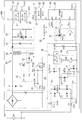
次に、図2を参照して電源システム100の構成について説明する。上述したように、電源システム100は、電源部10と制御装置50とを含む。まず、電源システム100の電源部10の構成について説明する。電源部10は、スイッチング電源20および小容量電源回路30を含む。
2. Next, the configuration of the
スイッチング電源20は、整流平滑回路21、制御IC22、電圧発生回路23、トランス24、FET(電界効果トランジスタ)Q1、整流平滑回路25、電圧検出回路26、およびDC−DCコンバータ27、28を含む。
The
スイッチング電源20は、交流電源ACの交流電圧Vacを整流平滑化し、通常モードにおいて+24V、+5Vおよび+3.3Vの直流電圧を生成する。+24Vの直流電圧(以下「DC24V」と記す)は第1出力端子OUT1から出力され、+5Vの直流電圧(以下「DC5V」と記す)は第2出力端子OUT2から出力され、+3.3Vの直流電圧(以下「DC3.3V」と記す)は第3出力端子OUT3から出力される。
The
整流平滑回路21は、いわゆるコンデンサインプット型であり、交流電源ACの交流電圧Vac(例えば、240V)を整流するブリッジダイオードおよび整流後の電圧を平滑化するコンデンサを含む。整流平滑回路21の出力は、トランス24の一次コイルに印加される。
The rectifying and smoothing
トランジスタQ1はNチャンネルのMOSFETであり、制御IC22からゲートにオン・オフ信号(PWM信号)が与えられることにより、オン・オフ動作する。これにより、トランス24の一次側が発振して、トランス24の二次コイルに電圧を誘起させる。
The transistor Q1 is an N-channel MOSFET, and is turned on and off when an ON / OFF signal (PWM signal) is supplied from the
また、トランス24の一次側には電圧発生回路23が設けられている。電圧発生回路23は、トランス24の一次側に設けられた補助コイルに誘起される電圧を整流平滑化して、制御IC22用の電源電圧Vccを生成する。
A
整流平滑回路25はトランス24の二次コイルに誘起された電圧を整流平滑化してDC24Vを生成する。
The rectifying /
電圧検出回路26は、フォトカプラPC1を含み、スイッチング電源20のDC24V出力の検出レベルに応じて、フォトカプラPC1の発光ダイオードLED1を発光させる。フォトカプラPC1は、制御IC22のフィードバックポートFBに接続されたフォトトランジスタPT1を含む。そのため、発光ダイオードLED1の光信号はフォトトランジスタPT1にて電気信号に戻され、DC24V出力の検出値が制御IC22のフィードバックポートFBにフィードバックされる。
The
DC−DCコンバータ27は、DC24VをDC5Vに変換して出力し、DC−DCコンバータ28は、DC24VをDC3.3Vに変換して出力する。
The DC-
制御IC22は、制御入力ポートENに入力される制御パルス信号Scpに応じてトランジスタQ1へのオン・オフ信号を制御し、トランス24の一次側の発振を制御する。通常モードにおいては、トランス24の一次側を発振させて、各DC電圧を生成し、省電力モードにおいては、トランジスタQ1へのオン・オフ信号の出力を停止して、トランス24の一次側の発振を停止させる。すなわち、省電力モードにおいては、スイッチング電源20からDC電圧は出力されない。なお、プリンタ1の省電力モードから通常モードへの復帰時には、制御装置50から制御パルス信号Scpが制御入力ポートENに入力され、制御パルス信号Scpに応じてトランス24の一次側の発振が開始され、各DC電圧がスイッチング電源20から出力される。すなわち、プリンタ1の通常モードにおいてスイッチング電源20は出力モードとされ、プリンタ1の省電力モードにおいてスイッチング電源20は出力停止モードとされる。なお、入力ポートVHには、スイッチング電源20の始動時に電源電圧が供給される。
The
次に、電源システム100の制御装置50の構成について説明する。制御装置50は、ASIC(特定用途向けIC)51とスイッチング電源制御部52とを含む。ASIC51は、プリンタ1の印刷部2を制御するメインブロックB1と、主にプリンタ1のモード制御を行うモード制御ブロックB2とから構成されている。なお、モード制御の一部はメインブロックB1で行うようにしてもよい。また、メインブロックB1およびモード制御ブロックB2は、ASIC51で構成されることに限られない。例えば、メインCPUとサブCPUによって構成されてもよい。
Next, the configuration of the
メインブロックB1の電源ポートP1は、スイッチング電源20のDC−DCコンバータ28からDC3.3Vを受け取る。なお、メインブロックB1は通常モード中に限り電力が供給されて動作状態となり、スイッチング電源20が出力停止モード、すなわち、省電力モードに移行すると、電力の供給が断たれて停止状態になる。
The power supply port P1 of the main block B1 receives DC 3.3V from the DC-
また、メインブロックB1は、タイマ55、メモリ56を含み、後述するように、ゼロクロス検出回路34からポートP5に入力されるパルス信号Pzcに基づいて、交流電源ACの交流電圧Vacのゼロクロス点ZP(図3参照)を検出する。そして、メインブロックB1は、ゼロクロス点ZPに基づいてゼロクロス信号Szcを生成し(図3参照)、ゼロクロス信号Szcに基づいて、例えば、定着器2fの通電制御を行う。
The main block B1 includes a
タイマ55は、ゼロクロス点ZPを検出する際の時間計測に利用される。メモリ56は、ROMおよびRAMを含む。ROMには、ASIC51が実行する各種プログラムが格納され、RAMにはプログラムが実行される際の各種データが格納される。
The
一方、モード制御ブロックB2の電源ポートP2は、小容量電源回路30のDC−DCコンバータ33に接続されており、通常モードおよび省電力モードにおいて小容量電源回路30から電力供給される。モード制御ブロックB2は、プリンタ1のモード切り換えに応じて、スイッチング電源20を、出力モードと、スイッチング電源20の発振を停止させる出力停止モードとに切り換え制御する。
On the other hand, the power supply port P2 of the mode control block B2 is connected to the DC-
すなわち、モード制御ブロックB2は、制御IC22に対して制御パルス信号Scpを出力することにより、スイッチング電源20を出力モードと出力停止モードとに切り換える。ここで、出力モードとは、トランス24の一次側を発振させて、スイッチング電源20を出力状態にするモードであり、通常モードに対応する。一方、出力停止モードは、トランス24の発振を停止させてスイッチング電源20の出力を停止させるモードであり、省電力モードに対応する。このように、省電力モードにおいては、スイッチング電源20の出力が停止されるため、制御装置50には、すなわち、ASIC51のモード制御ブロックB2およびスイッチング電源動作制御部52には、小容量電源回路30から電力が供給される。
That is, the mode control block B2 switches the switching
スイッチング電源動作制御部52は、フォトカプラPC2の発光ダイオードLED2およびトランジスタQ2を含む。発光ダイオードLED2のアノードは、DC−DCコンバータ33からの直流+3.3V(以下、DC3.3VBと記す)の電源ラインに接続されている。
Switching power supply
発光ダイオードLED2は、スイッチング電源20の制御IC22の制御入力ポートENに接続されたフォトトランジスタPT2と共に、フォトカプラPC2を構成している。そのため、モード制御ブロックB2の制御ポートP3からトランジスタQ2のベースに制御パルス信号Scpが出力されると、制御パルス信号Scpは、フォトカプラPC2を介して光伝送され、制御IC22の制御入力ポートENに入力される。
The light emitting diode LED2 and the phototransistor PT2 connected to the control input port EN of the
このように、制御装置50は、詳しくは、ASIC51のモード制御ブロックB2は、省電力モードから通常モードへ切り換える場合、小容量電源回路30から供給される電力によって、スイッチング電源20の発振を再開させる制御パルス信号Scpを生成し、制御パルス信号Scpをスイッチング電源20に送出する。そのため、省電力モードから通常モードへの切り換えを、省電力モード時に蓄えられた電力を利用して好適に行える。
また、ユーザは、スイッチS1によって、モード制御ブロックB2にモードの切り換えを指示することができる。
As described above, in detail, the
Further, the user can instruct the mode control block B2 to switch the mode using the switch S1.
なお、モード制御ブロックB2のポートP4からは、スイッチング電源20のDC−DCコンバータ28の動作をオン・オフ制御する制御信号Sconが出力される。そして、例えば、通常モードにおいても、小容量電源回路30から供給されるDC3.3VBの電力で事足りる場合には、AISC51は、制御信号Sconによってスイッチング電源20のDC−DCコンバータ28の動作を停止させる。
A control signal Scon for on / off control of the operation of the DC-
3.小容量電源回路の構成
次に、小容量電源回路30について説明する。小容量電源回路30は省電力モードおよび通常モードにおいて制御装置50に電力を供給する。詳しくは、小容量電源回路30は、各モードにおいて、制御装置50のモード制御ブロックB2およびスイッチング電源動作制御部52に電力を供給する。通常モードにおいては、小容量電源回路30は、交流電圧Vacの大きさに応じて、交流電源ACから制御装置50に電力を供給したり、ダイオードD5を介してスイッチング電源20のDC5Vから電力を供給したりする。省電力モードにおいては、小容量電源回路30は、平滑コンデンサC3から制御装置50に電力を供給する。また、通常モードにおいて交流電源ACのゼロクロス点を検出するための構成を含む。
3. Next, the small-capacity
小容量電源回路30は、第1コンデンサC1、第2コンデンサC2、整流回路31、ツェナーダイオードZD1、平滑コンデンサC3、DC−DCコンバータ33、ゼロクロス検出用パルス生成回路34および蓄電用コンデンサC4を含む。
The small-capacity
第1コンデンサC1は、第1電極C1p1および第2電極C1p2を有し、第1電極C1p1が交流電源ACの一端に接続され、第2電極C1p2が整流回路31に接続される。また、第2コンデンサC2は、第1電極C2p1および第2電極C2p2を有し、第1電極C2p1が交流電源ACの他端に接続され、第2電極C2p2が整流回路31に接続される。
The first capacitor C1 has a first electrode C1p1 and a second electrode C1p2, the first electrode C1p1 is connected to one end of the AC power supply AC, and the second electrode C1p2 is connected to the
整流回路31は、第1コンデンサC1の第2電極C1p2と第2コンデンサC2の第2電極との間に電気的に接続され、両コンデンサC1、C2に印加される交流電圧Vacを整流する。実施形態1では、整流回路31は、4個のダイオードD1,D2,D3,D4からなるブリッジ回路によって構成される。ダイオードD1およびダイオードD2のカソードは第1接続点Nd1において接続され、ダイオードD1のアノードは第1コンデンサC1の第2電極C1p2に接続され、ダイオードD2のアノードは第2コンデンサC2の第2電極C2p2に接続される。
The
また、ダイオードD3およびダイオードD4のアノードは第2接続点Nd2において接続され、ダイオードD3のカソードは第1コンデンサC1の第2電極C1p2に接続され、ダイオードD4のカソードは第2コンデンサC2の第2電極C2p2に接続される。第2接続点Nd2は基準電位配線Lgdに接続される。なお、実施形態1では、電源システム100はフレーム接地されており、それにより基準電位配線Lgdも接地され、基準電位配線Lgdの電位は0Vである。
The anodes of the diode D3 and the diode D4 are connected at the second connection point Nd2, the cathode of the diode D3 is connected to the second electrode C1p2 of the first capacitor C1, and the cathode of the diode D4 is the second electrode of the second capacitor C2. Connected to C2p2. The second connection point Nd2 is connected to the reference potential wiring Lgd. In the first embodiment, the
平滑コンデンサC3は、整流回路31に接続され、整流された交流電圧を平滑して平滑電圧Vchを生成する。平滑コンデンサC3は、ダイオードD5を介してスイッチング電源20のDC5Vの出力端(第2出力端子)OUT2に電気的に接続される。そのため、プリンタ1の電源投入時には、スイッチング電源20のDC5Vによって平滑コンデンサC3および蓄電用コンデンサC4に短時間で充電が可能となる。
The smoothing capacitor C3 is connected to the
ダイオードD5は平滑コンデンサC3からDC−DCコンバータ27側への逆流を防止するものである。また、ツェナーダイオードZD1は、交流電源ACの交流電圧Vacが上昇した場合に、平滑電圧Vchの上昇を抑制するためのものである。
The diode D5 prevents a back flow from the smoothing capacitor C3 to the DC-
DC−DCコンバータ33は、平滑電圧VchをDC3.3VBに変換する。DC3.3VBは、スイッチング電源動作制御部40およびモード制御ブロックB2の電源ポートP2に供給される。すなわち、モード制御ブロックB2の電力は、小容量電源回路30から供給される。
The DC-
蓄電用コンデンサC4は、DC−DCコンバータ33からのDC3.3VBによって充電される。充電電力は、省電力モードから通常モードに切り換わる際に、フォトカプラPC2のLED2の駆動電流に使用される。また、平滑コンデンサC3および蓄電用コンデンサC4の容量を適宜に選定することによって、省電力モードにおいて、所定電圧の必要に応じた電力量を蓄電することができる。実施形態1では、フォトカプラPC2の発光ダイオードLED2を確実に駆動させる電力量を蓄電することができる平滑コンデンサC3および蓄電用コンデンサC4が用いられる。そのため、スイッチング電源20を確実に再起動させることができる。
The storage capacitor C4 is charged by DC 3.3VB from the DC-
ゼロクロス検出用パルス生成回路(以下、単に、「パルス生成回路」と記す)34は、整流回路31の後段の電流経路IPに接続され、電流経路IPに流れる整流電流Ircに基づいて交流電源ACのゼロクロス点ZP、すなわちゼロクロスタイミングを検出する。詳しくは、パルス生成回路34は、ゼロクロス点ZPに対応したゼロクロス検出用パルス信号(以下、単に、「パルス信号」と記す)Pzcを生成し、パルス信号Pzcに基づいて、ASIC51のメインブロックB1が最終的にゼロクロス点ZPを検出する。したがって、ゼロクロス検出用パルス生成回路34およびメインブロックB1が、「ゼロクロス検出回路」に相当する。
A zero-cross detection pulse generation circuit (hereinafter simply referred to as “pulse generation circuit”) 34 is connected to a current path IP subsequent to the
パルス生成回路34は、図2に示されるように、抵抗R1、抵抗R2、ダイオードD6、およびNPNトランジスタ(以下、単に「トランジスタ」と記す)Q3を含む。
As shown in FIG. 2, the
電流経路IPは、整流回路31の第1接続点Nd1から平滑コンデンサC3および抵抗R1を介して基準電位線Lgdに至る経路であり、整流電流Ircが流れる。言い換えれば、電流経路IPは、交流電源ACから出力される交流電流Iacが交流電源ACに戻る際に、交流電流Iacが経由する経路となっている。
The current path IP is a path from the first connection point Nd1 of the
トランジスタQ3は、整流電流Ircが電流経路IPに流れることによって生成されるベース電流によってスイッチング動作するスイッチングトランジスタとして動作する。すなわち、トランジスタQ3は、整流電流Ircをパルス信号Pzcに変換する。 The transistor Q3 operates as a switching transistor that performs a switching operation by a base current generated when the rectified current Irc flows through the current path IP. That is, the transistor Q3 converts the rectified current Irc into the pulse signal Pzc.
詳しくは、トランジスタQ3のコレクタは抵抗R2の一端に接続され、ベースが電流経路IPに接続され、エミッタは基準電位線Lgdに接続される。抵抗R2はプルアップ抵抗であり、その他端はDC−DCコンバータ28のOUT3のDC3.3Vに接続されている。
Specifically, the collector of the transistor Q3 is connected to one end of the resistor R2, the base is connected to the current path IP, and the emitter is connected to the reference potential line Lgd. The resistor R2 is a pull-up resistor, and the other end is connected to DC3.3V of OUT3 of the DC-
トランジスタQ3はベースに供給されるベース電流に応じてオン・オフされる。また、パルス信号Pzcは、トランジスタQ3のコレクタから出力され、トランジスタQ3がオン時にはゼロVとなり、トランジスタQ3がオフ時に3.3Vとなる。ASIC51は、パルス信号Pzcのパルス周期Tpを検出し、パルス周期Tpを用いて交流電源ACの交流電圧Vacのゼロクロス点ZPを検出する(図3参照)。
The transistor Q3 is turned on / off according to the base current supplied to the base. Further, the pulse signal Pzc is output from the collector of the transistor Q3, and becomes zero V when the transistor Q3 is turned on, and becomes 3.3 V when the transistor Q3 is turned off. The
なお、トランジスタQ3は、NPNトランジスタに限られない。また、パルス信号Pzcを生成する構成は、必ずしもトランジスタQ3および抵抗R2の構成に限られない。例えば、トランジスタQ3はFETであってもよい。その際、整流電流Ircをゲート電圧に変換する電流−電圧変換回路を設ければよい。電流−電圧変換回路として、例えば、ボルテージフォロアのオペアンプが使用できる。 The transistor Q3 is not limited to an NPN transistor. Further, the configuration for generating the pulse signal Pzc is not necessarily limited to the configuration of the transistor Q3 and the resistor R2. For example, the transistor Q3 may be a FET. At that time, a current-voltage conversion circuit for converting the rectified current Irc into a gate voltage may be provided. For example, a voltage follower operational amplifier can be used as the current-voltage conversion circuit.
4.ゼロクロス点の検出方法
次に、図3を参照して、ゼロクロス点の検出方法を説明する。なお、図3には、交流電源ACの周波数=50Hz、交流電圧Vac=240V(実効値)、コンデンサC1,C2の容量=3300pF(ピコファラッド)、ダイオードD1〜D4の順電圧降下=0.6V、負荷電流=50μA、ツェナーダイオードZD1のツェナー電圧=8.2V、抵抗R1の抵抗値=15kΩ、および抵抗R2の抵抗値=10kΩとした場合の波形が示される。
4). Zero Cross Point Detection Method Next, a zero cross point detection method will be described with reference to FIG. In FIG. 3, the frequency of the AC power supply AC = 50 Hz, the AC voltage Vac = 240 V (effective value), the capacitances of the capacitors C1 and C2 = 3300 pF (picofarad), the forward voltage drop of the diodes D1 to D4 = 0.6V. The waveform when load current = 50 μA, Zener voltage of Zener diode ZD1 = 8.2V, resistance value of resistor R1 = 15 kΩ, and resistance value of resistor R2 = 10 kΩ is shown.
図3に示されるように、交流電圧Vacの増加に伴って、整流電流Irc(平滑コンデンサC3に流れる電流)とツェナーダイオードZD1との合計電流である経路電流Iipが増加する。図3の時刻t1において、経路電流Iipによって抵抗R1の電圧降下、すなわちトランジスタQ3のベース−エミッタ間電圧がトランジスタQ3のオン電圧を超えると、トランジスタQ3がオンされ、パルス信号Pzcは0Vとなる。時刻t1以後、交流電圧Vacの変化に伴って、経路電流Iipがさらに上昇する。その後、経路電流Iipが下降して、時刻t2において抵抗R1の電圧降下がトランジスタQ3のオン電圧以下となると、トランジスタQ3がオフされ、パルス信号Pzcは、ほぼ3.3Vとなる。 As shown in FIG. 3, the path current Iip, which is the total current of the rectified current Irc (current flowing through the smoothing capacitor C3) and the Zener diode ZD1, increases with the increase of the AC voltage Vac. At time t1 in FIG. 3, when the voltage drop of the resistor R1, that is, the base-emitter voltage of the transistor Q3 exceeds the on-voltage of the transistor Q3 due to the path current Iip, the transistor Q3 is turned on and the pulse signal Pzc becomes 0V. After time t1, the path current Iip further increases with the change in the AC voltage Vac. Thereafter, when the path current Iip decreases and the voltage drop of the resistor R1 becomes equal to or lower than the on-voltage of the transistor Q3 at time t2, the transistor Q3 is turned off and the pulse signal Pzc becomes approximately 3.3V.
ASIC51のタイマ55は、図3の時刻t1においてパルス信号Pzcが0Vになると、パルス信号Pzcが0Vである期間K1(時刻t1〜時刻t2)の計測を開始する。
When the pulse signal Pzc becomes 0V at time t1 in FIG. 3, the
また、タイマ55は、図3の時刻t2においてパルス信号Pzcが3.3Vになると、パルス信号Pzcが3.3Vである期間K2(時刻t2〜時刻t3)の計測を開始する。ここで、期間K1+期間K2、すなわち、時刻t1〜時刻t3はパルス信号Pzcのパルス周期Tpに相当し、タイマ55は、パルス信号Pzcのパルス周期Tpを検出する。そして、ASIC51は、パルス信号Pzcのパルス周期Tpに基づいてゼロクロス点ZP1を検出する。なお、実施形態1のパルス周期Tpは20ms(ミリ秒)となり、交流電圧Vacの周期と等しい。
Further, when the pulse signal Pzc becomes 3.3V at time t2 in FIG. 3, the
パルス周期Tpが、Tp=K1+K2の場合、ASIC51は、図3に示されるゼロクロス点ZP1の時刻t4を、
t4=t3+(K1/2) ……式1
として算出する。
When the pulse period Tp is Tp = K1 + K2, the
t4 = t3 + (K1 / 2) ......
Calculate as
また、ASIC51は、図3に示されるゼロクロス点ZP2の時刻t6を、
t6=t5+(K2/2) ……式2
として算出する。
Further, the
t6 = t5 + (K2 / 2) ......
Calculate as
ここで、図3の時刻t1およびt3は、パルス信号Pzcの立ち下がりタイミングであり、図3の時刻t2およびt5は、パルス信号Pzcの立ち上がりタイミングである。そのため、言いかえれば、ASIC51は、パルス信号Pzcの立ち上がりタイミングおよび立ち下がりタイミングに基づいて、ゼロクロス点ZPを検出する。
Here, times t1 and t3 in FIG. 3 are falling timings of the pulse signal Pzc, and times t2 and t5 in FIG. 3 are rising timings of the pulse signal Pzc. Therefore, in other words, the
以下、同様にして、ゼロクロス点ZP3〜ZP6の時刻t7〜t10を算出する。そして、ASIC51は、例えば、ゼロクロス点ZP1〜ZP6の時刻t4、t6〜t10において立ち上がるゼロクロス信号Szcを生成し、ゼロクロス信号Szcに基づいて、例えば、定着器2fの通電制御を行う。
Thereafter, similarly, times t7 to t10 of the zero cross points ZP3 to ZP6 are calculated. For example, the
5.実施形態1の効果
ゼロクロス検出回路を構成するパルス生成回路34は、省電力モードに利用される小容量電源回路30に設けられ、小容量電源回路30の整流電流Ircを利用してゼロクロス検出が行われる。小容量電源回路30の整流電流Ircは、スイッチング電源20の整流電流と比べてはるかに小さい。そのため、小容量電源回路30に流れる整流電流Ircを利用してゼロクロス検出を行うことによって、より省電力化の可能な、ゼロクロス点の検知を行える。ちなみに、実施形態1のゼロクロス検出での消費電力量は、約80μWであり、従来のフォトカプラを用いたゼロクロス検出に比べてはるかに小さい。
5. Effects of
また、パルス生成回路34(ゼロクロス検出回路の一例)は、平滑コンデンサC3と基準電位配線Lgdとを結ぶ電流経路IPに接続される。このような電流経路IPは所定の平滑電圧Vchを生成するために、必要なものである。そのため、ゼロクロス検出のために、新たにゼロクロス検出のための専用の電流経路を設けることなく、元々必要な経路を利用できる。 The pulse generation circuit 34 (an example of a zero cross detection circuit) is connected to a current path IP that connects the smoothing capacitor C3 and the reference potential wiring Lgd. Such a current path IP is necessary to generate a predetermined smoothing voltage Vch. Therefore, originally necessary paths can be used for zero cross detection without newly providing a dedicated current path for zero cross detection.
<実施形態2>
次に、図4を参照して電源システム100の実施形態2を説明する。図4は、実施形態2における小容量電源回路30Aの構成を示す。なお、実施形態1の電源システム100とは、小容量電源回路においてパルス生成回路34が設けられる電流経路のみが異なる。そのため、その相違点を説明し、同一構成についてはその説明を省略する。
<
Next,
実施形態2においては、パルス生成回路34(ゼロクロス検出回路の一例)は、整流電流Ircを分流させる専用電流経路IPsに接続される。詳しくは、図4に示されるように、専用電流経路IPsは、直列接続された二個の分圧抵抗R1,R3によって構成されるとともに、整流回路31と平滑コンデンサC3との間において、平滑コンデンサC3と並列接続される。そして、パルス生成回路34は二個の分圧抵抗R1,R3の間に接続される。具体的には、パルス生成回路34のトランジスタQ3のベースが二個の分圧抵抗R1,R3の間に接続される。そして、整流電流Ircの分流Irc1によってトランジスタQ3がオン・オフされ、実施形態1と同等に、ゼロクロス検出が行われる。
In the second embodiment, the pulse generation circuit 34 (an example of a zero cross detection circuit) is connected to a dedicated current path IPs that shunts the rectified current Irc. Specifically, as shown in FIG. 4, the dedicated current path IPs is constituted by two voltage-dividing resistors R1 and R3 connected in series, and between the
この構成では、ゼロクロスを検出するためのパルス生成回路34と、平滑回路35とが、ダイオードD7によって分離され、半波整流されたVchaの電圧によりゼロクロスを検出し、その後、平滑化された電圧Vchbとなる。すなわち、実施形態1と比べ、平滑化された電圧が安定するため、DC−DCコンバータ33で生成される+3.3VBが、より安定する。
In this configuration, the
<実施形態3>
次に、図5を参照して電源システム100の実施形態3を説明する。図5は、実施形態3における小容量電源回路30Bの構成を示す。なお、実施形態1の電源システム100とは、実施形態2と同様に、小容量電源回路においてパルス生成回路34が設けられる電流経路のみが異なる。そのため、その相違点を説明し、同一構成についてはその説明を省略する。
<
Next, a third embodiment of the
実施形態3においては、実施形態2と同様に、パルス生成回路34(ゼロクロス検出回路の一例)は専用電流経路IPsに接続される。詳しくは、図5に示されるように、整流回路31と平滑コンデンサC3との間に抵抗R4が接続される。そして、専用電流経路IPsは、抵抗R4の電圧降下によってオン・オフされるトランジスタQ4(スイッチ回路の一例)と、トランジスタQ4と基準電位配線Lgdとの間に接続された二個の分圧抵抗R1,R3によって構成される。そして、パルス生成回路34は二個の分圧抵抗R1,R3の間に接続される。具体的には、パルス生成回路34のトランジスタQ3のベースが二個の分圧抵抗R1,R3の間に接続される。
In the third embodiment, as in the second embodiment, the pulse generation circuit 34 (an example of a zero cross detection circuit) is connected to the dedicated current path IPs. Specifically, as shown in FIG. 5, a resistor R4 is connected between the
この構成では、整流電流Ircが所定電流以上(抵抗R4の電圧降下が所定以上)のときにのみ、トランジスタQ4がオンされて、整流電流Ircの分流Irc2に基づいてゼロクロス検出が行われる。このように、整流電流Ircの電流量が所定量、確保される場合にのみゼロクロス検出が行われるため、ゼロクロス検出の信頼性が向上する。 In this configuration, the transistor Q4 is turned on only when the rectified current Irc is equal to or greater than a predetermined current (the voltage drop across the resistor R4 is equal to or greater than a predetermined value), and zero-cross detection is performed based on the shunt current Irc2 of the rectified current Irc. As described above, the zero-cross detection is performed only when a predetermined amount of the rectified current Irc is ensured, so that the reliability of the zero-cross detection is improved.
<他の実施形態>
本発明は上記記述及び図面によって説明した実施形態に限定されるものではなく、例えば次のような実施形態も本発明の技術的範囲に含まれる。
<Other embodiments>
The present invention is not limited to the embodiments described with reference to the above description and drawings. For example, the following embodiments are also included in the technical scope of the present invention.
(1)実施形態1において、ツェナーダイオードZD1および平滑コンデンサC3を設ける例を示したがこれに限られず、ツェナーダイオードZD1および平滑コンデンサC3のいずれか一方を設けるようにしてもよい。この場合であっても、ゼロクロス検出回路34は、電流経路IPに流れる整流電流Ircに基づいて交流電源のゼロクロス点を検出することができる。
また、平滑コンデンサC3が設けられる場合、抵抗R1およびダイオードD6の少なくとも一方が設けられればよい。
(1) In the first embodiment, an example in which the Zener diode ZD1 and the smoothing capacitor C3 are provided has been described. However, the present invention is not limited to this, and either the Zener diode ZD1 or the smoothing capacitor C3 may be provided. Even in this case, the zero
Further, when the smoothing capacitor C3 is provided, at least one of the resistor R1 and the diode D6 may be provided.
(2)実施形態2および実施形態3において、DC−DCコンバータ33および蓄電用コンデンサC4が設けられる場合、ツェナーダイオードZD1および平滑コンデンサC3は省略されてもよい。
(2) In the second and third embodiments, when the DC-
(3)上記各実施形態において、制御装置50、詳しくは、ASIC51のメインブロックB1は、パルス信号(ゼロクロスパルスに相当)Pzcが検出されない場合、交流電源ACの電圧Vacが低下した、あるいは交流電源ACが不意にオフされたと判断し、電源異常信号を生成するようにしてもよい。これは、パルス信号Pzcが検出されない場合には、交流電源ACの電圧低下、あるいは交流電源ACがオフされたことを検出できることによる。この場合、電源異常が発生した場合、好適に対処できる。
(3) In each of the above embodiments, the
(4)上記各実施形態において、制御装置50、詳しくは、ASIC51のメインブロックB1は、ゼロクロス信号(ゼロクロスパルスに相当)Pzcの期間K1(パルス幅に相当)が所定期間より短い場合、矩形波の交流電源ACが入力されたと判断し、矩形波電源異常信号を生成するようにしてもよい。
(4) In each of the above embodiments, the
これは、交流電源ACの波形が矩形波の場合、パルス信号Pzcの期間K1が非常に短くなる。そのため、期間K1を、矩形波を検出するための所定時間と比較し、期間K1が所定時間より短い場合、交流電源ACが矩形波であることを検出できることによる。すなわち、パルス信号Pzcの期間K1に基づいて、ゼロクロス点ZPを検出できるとともに、交流電源ACの波形異常を検出することができる。そのため、矩形波の交流電源ACが入力された場合、好適に対処できる。 This is because the period K1 of the pulse signal Pzc becomes very short when the waveform of the AC power supply AC is a rectangular wave. Therefore, the period K1 is compared with a predetermined time for detecting a rectangular wave, and when the period K1 is shorter than the predetermined time, it can be detected that the AC power supply AC is a rectangular wave. In other words, based on the period K1 of the pulse signal Pzc, the zero cross point ZP can be detected, and the waveform abnormality of the AC power supply AC can be detected. Therefore, when a rectangular wave AC power supply AC is input, it is possible to cope with it appropriately.
(5)上記各実施形態において、平滑コンデンサC3を、ダイオードD5を介してスイッチング電源20のDC5V出力(OUT2)に接続する構成は、必ずしも必要な構成ではなく、省略されてもよい。すなわち、平滑コンデンサC3はスイッチング電源20の第2出力端子OUT2に接続されなくてもよい。
(5) In each of the above embodiments, the configuration in which the smoothing capacitor C3 is connected to the DC5V output (OUT2) of the switching
(6)上記各実施形態において、定電圧回路であるツェナーダイオードZD1は、必ずしも必要な構成ではなく、省略されてもよい。また、DC−DCコンバータ33および蓄電用コンデンサC4は、必ずしも必要な構成ではなく、省略されてもよい。その際、フォトカプラPC2のLED2の駆動電流は、平滑コンデンサC3から供給されることとなる。
(6) In each of the embodiments described above, the Zener diode ZD1 that is a constant voltage circuit is not necessarily a necessary configuration and may be omitted. Further, the DC-
(7)上記各実施形態において、整流回路31の構成は、図2等に示される4個のダイオードD1〜D4によって構成されるものに限定されない。例えば、図6に示される整流回路31Aのように、二個のダイオードD2およびD4によって構成されてもよい。
(7) In each of the embodiments described above, the configuration of the
(8)上記各実施形態においては、基準電位配線Lgdが接地されている例を示したがこれに限られず、本発明は、基準電位配線Lgdが接地されていない場合にも適用できる。 (8) In each of the above embodiments, the example in which the reference potential wiring Lgd is grounded has been described. However, the present invention is not limited to this, and the present invention can also be applied to the case where the reference potential wiring Lgd is not grounded.
(9)上記各実施形態において、本明細書によって開示される電源システム100を画像形成装置に適用した例を示すが、これに限られない。電源システム100は、通常モードと省電力モードとを有するあらゆる装置に適用できる。
(9) In each of the above embodiments, an example in which the
1…プリンタ、20…スイッチング電源、30…小容量電源回路、31…整流回路、34…ゼロクロス検出用パルス生成回路、50…制御装置、100…電源システム、C1…第1コンデンサ、C2…第2コンデンサ、C3…平滑コンデンサ、IP…電流経路、IPs…専用電流経路、Irc…整流電流。
DESCRIPTION OF
Claims (8)
前記スイッチング電源を、前記通常モードと、前記スイッチング電源の発振を停止させる省電力モードとに切り換え制御する制御装置と、
前記省電力モードにおいて前記制御装置に電力を供給する小容量電源回路であって、
第1電極および第2電極を有し、当該第1電極が前記交流電源の一端に接続される第1コンデンサと、
第1電極および第2電極を有し、当該第1電極が前記交流電源の他端に接続される第2コンデンサと、
前記第1コンデンサの前記第2電極と前記第2コンデンサの前記第2電極との間に電気的に接続され、両コンデンサに印加される交流電圧を整流する整流回路と、
前記整流回路に接続され、整流された交流電圧を平滑して平滑電圧を生成する平滑コンデンサとを含む小容量電源回路とを備え、
前記小容量電源回路は、前記整流回路の後段の電流経路であって、前記平滑コンデンサの充電時に流れる電流および前記平滑コンデンサの放電時に流れる電流の経路となる電流経路に接続され、前記電流経路に流れる整流電流に基づいて前記交流電源のゼロクロス点を検出するゼロクロス検出回路を含む、電源システム。 A switching power supply that rectifies and smoothes the AC voltage of the AC power supply and generates a predetermined DC voltage in a normal mode in which oscillation is performed;
A control device for switching and controlling the switching power supply between the normal mode and a power saving mode for stopping oscillation of the switching power supply;
A small capacity power supply circuit for supplying power to the control device in the power saving mode,
A first capacitor having a first electrode and a second electrode, wherein the first electrode is connected to one end of the AC power source;
A second capacitor having a first electrode and a second electrode, wherein the first electrode is connected to the other end of the AC power source;
A rectifier circuit that is electrically connected between the second electrode of the first capacitor and the second electrode of the second capacitor and rectifies an AC voltage applied to both capacitors ;
A small-capacity power supply circuit including a smoothing capacitor connected to the rectifier circuit and smoothing the rectified AC voltage to generate a smoothed voltage ;
The small-capacity power supply circuit is connected to a current path that is a subsequent current path of the rectifier circuit and serves as a path of a current that flows when the smoothing capacitor is charged and a current that flows when the smoothing capacitor is discharged. A power supply system including a zero cross detection circuit that detects a zero cross point of the AC power supply based on a flowing rectified current.
前記ゼロクロス検出回路は、前記平滑コンデンサと、前記平滑コンデンサに対して前記整流回路が接続される側とは反対側に接続される基準電位配線との間に接続される、電源システム。 The power supply system according to claim 1,
The zero-cross detection circuit, the smoothing capacitor, wherein the said side of the rectifier circuit is connected to a smoothing capacitor is connected between the reference potential wiring connected to the opposite side, the power supply system.
前記ゼロクロス検出回路は、カソードが前記平滑コンデンサに接続され、アノードが前記基準電位配線に接続されるダイオードと、ベースが前記平滑コンデンサおよび前記カソードに接続され、エミッタが前記基準電位配線および前記アノードに接続されるトランジスタとを含む、電源システム。The zero-cross detection circuit includes a diode having a cathode connected to the smoothing capacitor, an anode connected to the reference potential wiring, a base connected to the smoothing capacitor and the cathode, and an emitter connected to the reference potential wiring and the anode. A power supply system including a connected transistor.
前記平滑コンデンサは、前記スイッチング電源により生成された直流電圧によって充電される、電源システム。The smoothing capacitor is charged by a DC voltage generated by the switching power supply.
前記ゼロクロス検出回路は、ゼロクロス点に対応したゼロクロスパルスを検出し、前記ゼロクロスパルスに基づいて前記ゼロクロス点を検出し、
前記制御装置は、前記ゼロクロスパルスが検出されない場合、前記交流電源の電圧が低下した、あるいは前記交流電源が不意にオフされたと判断し、電源異常信号を生成する、電源システム。 In the power supply system according to any one of claims 1 to 4 ,
The zero cross detection circuit detects a zero cross pulse corresponding to a zero cross point, detects the zero cross point based on the zero cross pulse,
When the zero cross pulse is not detected, the control device determines that the voltage of the AC power supply has decreased or that the AC power supply has been turned off unexpectedly, and generates a power supply abnormality signal.
前記ゼロクロス検出回路は、ゼロクロス点に対応したゼロクロスパルスを検出し、前記ゼロクロスパルスに基づいて前記ゼロクロス点を検出し、
前記制御装置は、前記ゼロクロスパルスのパルス幅が所定パルス幅より短い場合、矩形波の交流電源が入力されたと判断し、矩形波電源異常信号を生成する、電源システム。 In the power supply system according to any one of claims 1 to 4 ,
The zero cross detection circuit detects a zero cross pulse corresponding to a zero cross point, detects the zero cross point based on the zero cross pulse,
When the pulse width of the zero cross pulse is shorter than a predetermined pulse width, the control device determines that a rectangular wave AC power supply has been input and generates a rectangular wave power supply abnormality signal.
請求項1から請求項6のいずれか一項に記載の電源システムを備える画像形成装置。 An image forming apparatus having a normal mode and a power saving mode,
An image forming apparatus comprising the power supply system according to any one of claims 1 to 6 .
第1電極および第2電極を有し、当該第1電極が前記交流電源の他端に接続される第2コンデンサと、
前記第1コンデンサの前記第2電極と前記第2コンデンサの前記第2電極との間に電気的に接続され、両コンデンサに印加される交流電圧を整流する整流回路と、
前記整流回路に接続され、整流された交流電圧を平滑して平滑電圧を生成する平滑コンデンサと、
前記整流回路の後段の電流経路であって、前記平滑コンデンサの充電時に流れる電流および前記平滑コンデンサの放電時に流れる電流の経路となる電流経路に接続され、前記電流経路に流れる整流電流に基づいて前記交流電源のゼロクロス点を検出するゼロクロス検出回路と、
を備えた小容量電源回路。 A first capacitor having a first electrode and a second electrode, wherein the first electrode is connected to one end of an AC power source;
A second capacitor having a first electrode and a second electrode, wherein the first electrode is connected to the other end of the AC power source;
A rectifier circuit that is electrically connected between the second electrode of the first capacitor and the second electrode of the second capacitor and rectifies an AC voltage applied to both capacitors;
A smoothing capacitor connected to the rectifier circuit and smoothing the rectified AC voltage to generate a smoothed voltage;
A current path downstream of the rectifier circuit , which is connected to a current path that is a current path that flows when the smoothing capacitor is charged and a current that flows when the smoothing capacitor is discharged, and based on the rectified current that flows through the current path A zero-cross detection circuit that detects the zero-cross point of the AC power supply;
A small capacity power supply circuit.
Priority Applications (4)
| Application Number | Priority Date | Filing Date | Title |
|---|---|---|---|
| JP2011241367A JP5780120B2 (en) | 2011-11-02 | 2011-11-02 | Power supply system, image forming apparatus equipped with the power supply system, and small-capacity power supply circuit |
| CN201210364448.2A CN103095160B (en) | 2011-11-02 | 2012-09-26 | Power-supply system, image forming apparatus and low capacity power circuit |
| EP12186338.5A EP2590308B1 (en) | 2011-11-02 | 2012-09-27 | Power supply system, image forming apparatus having the same, and low-capacity power supply circuit |
| US13/629,545 US9488944B2 (en) | 2011-11-02 | 2012-09-27 | Power saving power supply system having a low-capacity power supply circuit for use in an image forming apparatus |
Applications Claiming Priority (1)
| Application Number | Priority Date | Filing Date | Title |
|---|---|---|---|
| JP2011241367A JP5780120B2 (en) | 2011-11-02 | 2011-11-02 | Power supply system, image forming apparatus equipped with the power supply system, and small-capacity power supply circuit |
Publications (2)
| Publication Number | Publication Date |
|---|---|
| JP2013096902A JP2013096902A (en) | 2013-05-20 |
| JP5780120B2 true JP5780120B2 (en) | 2015-09-16 |
Family
ID=47257427
Family Applications (1)
| Application Number | Title | Priority Date | Filing Date |
|---|---|---|---|
| JP2011241367A Active JP5780120B2 (en) | 2011-11-02 | 2011-11-02 | Power supply system, image forming apparatus equipped with the power supply system, and small-capacity power supply circuit |
Country Status (4)
| Country | Link |
|---|---|
| US (1) | US9488944B2 (en) |
| EP (1) | EP2590308B1 (en) |
| JP (1) | JP5780120B2 (en) |
| CN (1) | CN103095160B (en) |
Families Citing this family (24)
| Publication number | Priority date | Publication date | Assignee | Title |
|---|---|---|---|---|
| JP5780120B2 (en) | 2011-11-02 | 2015-09-16 | ブラザー工業株式会社 | Power supply system, image forming apparatus equipped with the power supply system, and small-capacity power supply circuit |
| JP5834790B2 (en) | 2011-11-09 | 2015-12-24 | ブラザー工業株式会社 | Power supply system, image forming apparatus equipped with the same power supply system, and control method of power supply system |
| JP2013110789A (en) | 2011-11-17 | 2013-06-06 | Brother Ind Ltd | Power system, image forming apparatus having the same, and low capacity ac processing circuit |
| JP6056475B2 (en) | 2012-12-28 | 2017-01-11 | ブラザー工業株式会社 | Power supply system and image forming apparatus equipped with the power supply system |
| JP6304577B2 (en) | 2013-01-31 | 2018-04-04 | ブラザー工業株式会社 | Power supply system, image forming apparatus equipped with the same power supply system, and control method of power supply system |
| JP6111705B2 (en) | 2013-02-01 | 2017-04-12 | ブラザー工業株式会社 | Power system |
| JP6020219B2 (en) | 2013-02-06 | 2016-11-02 | ブラザー工業株式会社 | Power system |
| JP6044380B2 (en) | 2013-02-18 | 2016-12-14 | ブラザー工業株式会社 | Power supply system and image forming apparatus equipped with the power supply system |
| JP5974952B2 (en) * | 2013-03-27 | 2016-08-23 | ブラザー工業株式会社 | Power supply system and image forming apparatus equipped with the power supply system |
| JP6028653B2 (en) * | 2013-03-27 | 2016-11-16 | ブラザー工業株式会社 | Power supply system and image forming apparatus equipped with the power supply system |
| JP6155801B2 (en) | 2013-04-24 | 2017-07-05 | ブラザー工業株式会社 | Power supply system and image forming apparatus |
| JP6186858B2 (en) | 2013-05-01 | 2017-08-30 | ブラザー工業株式会社 | Power supply system and inkjet image forming apparatus |
| JP6249741B2 (en) * | 2013-11-29 | 2017-12-20 | キヤノン株式会社 | Information processing apparatus and control method of information processing apparatus |
| JP6269327B2 (en) * | 2014-06-04 | 2018-01-31 | 株式会社リコー | Control device and image forming apparatus |
| WO2016097476A1 (en) * | 2014-12-17 | 2016-06-23 | Salcomp Oyj | Switched-mode power supply |
| CN107847973B (en) * | 2015-05-11 | 2021-03-09 | 史赛克公司 | System and method for driving an ultrasonic handpiece with a linear amplifier |
| CN106569015B (en) * | 2015-10-13 | 2019-10-18 | 泰科电子(上海)有限公司 | AC load detection circuit |
| JP6066012B1 (en) * | 2016-09-21 | 2017-01-25 | 富士ゼロックス株式会社 | Power prediction apparatus, image forming apparatus, and power prediction program |
| WO2018205370A1 (en) * | 2017-05-12 | 2018-11-15 | 厦门赛特勒磁电有限公司 | Power conversion module |
| JP6819527B2 (en) * | 2017-09-22 | 2021-01-27 | ブラザー工業株式会社 | Detection device and machine tool |
| JP7080098B2 (en) * | 2018-04-24 | 2022-06-03 | エイブリック株式会社 | Zero cross detection circuit and sensor device |
| KR20200029196A (en) * | 2018-09-10 | 2020-03-18 | 휴렛-팩커드 디벨롭먼트 컴퍼니, 엘.피. | Power supply device to output zero-cross information of half ac wave |
| EP3648362B1 (en) * | 2018-11-02 | 2021-03-03 | Stmicroelectronics Sa | Method for limiting the level of voltage from a magnetic field received by a transponder and corresponding transponder |
| JP7458843B2 (en) * | 2020-03-23 | 2024-04-01 | 東芝テック株式会社 | power converter |
Family Cites Families (43)
| Publication number | Priority date | Publication date | Assignee | Title |
|---|---|---|---|---|
| JPS55130543U (en) * | 1979-03-08 | 1980-09-16 | ||
| JPS55130543A (en) | 1979-03-29 | 1980-10-09 | Coulter Systems Corp | Image forming electronic photograph medium and formation of electric charge image |
| JPS6130774A (en) * | 1984-07-24 | 1986-02-13 | Matsushita Electric Ind Co Ltd | Zero volt detection circuit |
| JPS6291265A (en) | 1985-10-15 | 1987-04-25 | Nankai:Kk | Apparatus for preparing base material for paint color sample book |
| JPS6291265U (en) * | 1985-11-26 | 1987-06-11 | ||
| US5166549A (en) * | 1991-08-07 | 1992-11-24 | General Electric Company | Zero-voltage crossing detector for soft-switching devices |
| JP3200258B2 (en) | 1993-09-16 | 2001-08-20 | キヤノン株式会社 | Power supply |
| US5914538A (en) | 1993-04-27 | 1999-06-22 | Canon Kabushiki Kaisha | Communication apparatus and power supply device therefor |
| JPH07308065A (en) * | 1994-05-10 | 1995-11-21 | Ricoh Co Ltd | Power supply |
| JPH0923638A (en) | 1995-07-07 | 1997-01-21 | Ricoh Co Ltd | Power supply |
| DE19652604A1 (en) * | 1996-04-23 | 1997-10-30 | Thomson Brandt Gmbh | Power supply for a device with standby operation |
| JP2000116027A (en) * | 1998-03-10 | 2000-04-21 | Fiderikkusu:Kk | Power supply device |
| US6320772B1 (en) * | 1999-05-26 | 2001-11-20 | Matsushita Electric Industrial Co., Ltd. | Converter circuit having control means with capability to short-circuit converter output |
| JP2001078446A (en) | 1999-06-29 | 2001-03-23 | Toshiba Corp | Power supply unit |
| US6969959B2 (en) | 2001-07-06 | 2005-11-29 | Lutron Electronics Co., Inc. | Electronic control systems and methods |
| CA2628211C (en) * | 2001-07-06 | 2014-09-16 | Lutron Electronics Company, Inc. | Electronic control systems and methods |
| JP2004056946A (en) * | 2002-07-22 | 2004-02-19 | Shindengen Electric Mfg Co Ltd | Switching power supply |
| JP3922159B2 (en) | 2002-10-30 | 2007-05-30 | ブラザー工業株式会社 | Heater driving device, fixing device, and image forming apparatus |
| JP2004303469A (en) | 2003-03-28 | 2004-10-28 | Brother Ind Ltd | Heating device and image formation device |
| JP4280244B2 (en) * | 2005-02-15 | 2009-06-17 | シャープ株式会社 | Job processing device |
| US20060209574A1 (en) * | 2005-03-17 | 2006-09-21 | Creative Technology, Ltd. | Power supply |
| CN2864700Y (en) * | 2005-11-01 | 2007-01-31 | 海信集团有限公司 | Zero-cross detecting circuit and refrigerator employing same |
| KR101235220B1 (en) | 2006-07-28 | 2013-02-20 | 삼성전자주식회사 | Phase detectiom device and phase controlling device having the same and fuser controlling device |
| AU2007358398B2 (en) | 2007-08-29 | 2011-03-17 | Mitsubishi Electric Corporation | AC/DC converter, and compressor driving unit and air conditioner utilizing the same |
| CN201110615Y (en) * | 2007-10-29 | 2008-09-03 | 珠海格力电器股份有限公司 | Zero-cross signal testing circuit of air conditioner controller as well as air conditioner |
| EP2104401B1 (en) | 2008-03-17 | 2013-08-14 | Universal Lighting Technologies, Inc. | Zero crossing detection of line voltage/current of variable amplitude |
| CN101265916B (en) * | 2008-05-12 | 2011-08-31 | 中南大学 | Electric fan speed governing control system and method |
| KR101497062B1 (en) | 2008-07-25 | 2015-03-05 | 페어차일드코리아반도체 주식회사 | Switch controller, switch control method, and converter using the same |
| JP2010054306A (en) * | 2008-08-27 | 2010-03-11 | Sharp Corp | Zero cross detection circuit, and image forming device including zero cross detection circuit |
| JP2010239774A (en) | 2009-03-31 | 2010-10-21 | Brother Ind Ltd | Zero-cross detection device |
| JP5056835B2 (en) * | 2009-11-26 | 2012-10-24 | ブラザー工業株式会社 | Heating apparatus and image forming apparatus |
| EP2510608B1 (en) * | 2009-12-07 | 2016-03-02 | Sigma Designs Israel S.D.I Ltd. | Enhanced power supply unit for powerline networks |
| JP2011199976A (en) | 2010-03-18 | 2011-10-06 | Panasonic Corp | Power source unit |
| JP5780812B2 (en) | 2010-05-12 | 2015-09-16 | キヤノン株式会社 | Voltage detection device and image heating device |
| EP2666237A1 (en) * | 2011-01-21 | 2013-11-27 | Hulusi Bulent Ertan | Power-level waveform generation method |
| JP5684064B2 (en) | 2011-07-28 | 2015-03-11 | ブラザー工業株式会社 | Zero-cross detection circuit and image forming apparatus having the detection circuit |
| JP5752513B2 (en) | 2011-07-29 | 2015-07-22 | ブラザー工業株式会社 | Power supply system and image forming apparatus having the same |
| JP5561255B2 (en) | 2011-08-09 | 2014-07-30 | ブラザー工業株式会社 | AC voltage detection circuit and image forming apparatus provided with the detection circuit |
| JP5780120B2 (en) | 2011-11-02 | 2015-09-16 | ブラザー工業株式会社 | Power supply system, image forming apparatus equipped with the power supply system, and small-capacity power supply circuit |
| JP5834790B2 (en) | 2011-11-09 | 2015-12-24 | ブラザー工業株式会社 | Power supply system, image forming apparatus equipped with the same power supply system, and control method of power supply system |
| JP2013110789A (en) | 2011-11-17 | 2013-06-06 | Brother Ind Ltd | Power system, image forming apparatus having the same, and low capacity ac processing circuit |
| JP6304577B2 (en) | 2013-01-31 | 2018-04-04 | ブラザー工業株式会社 | Power supply system, image forming apparatus equipped with the same power supply system, and control method of power supply system |
| JP6044380B2 (en) | 2013-02-18 | 2016-12-14 | ブラザー工業株式会社 | Power supply system and image forming apparatus equipped with the power supply system |
-
2011
- 2011-11-02 JP JP2011241367A patent/JP5780120B2/en active Active
-
2012
- 2012-09-26 CN CN201210364448.2A patent/CN103095160B/en active Active
- 2012-09-27 US US13/629,545 patent/US9488944B2/en active Active
- 2012-09-27 EP EP12186338.5A patent/EP2590308B1/en active Active
Also Published As
| Publication number | Publication date |
|---|---|
| US9488944B2 (en) | 2016-11-08 |
| CN103095160A (en) | 2013-05-08 |
| EP2590308B1 (en) | 2019-10-16 |
| EP2590308A2 (en) | 2013-05-08 |
| CN103095160B (en) | 2016-08-03 |
| US20130111237A1 (en) | 2013-05-02 |
| JP2013096902A (en) | 2013-05-20 |
| EP2590308A3 (en) | 2014-05-14 |
Similar Documents
| Publication | Publication Date | Title |
|---|---|---|
| JP5780120B2 (en) | Power supply system, image forming apparatus equipped with the power supply system, and small-capacity power supply circuit | |
| EP2595292B1 (en) | Power supply system, image forming apparatus having the same, and low-capacity AC processing circuit | |
| EP2552004B1 (en) | Power supply system with low power standby supply for control unit | |
| JP6056475B2 (en) | Power supply system and image forming apparatus equipped with the power supply system | |
| JP6304577B2 (en) | Power supply system, image forming apparatus equipped with the same power supply system, and control method of power supply system | |
| JP5974952B2 (en) | Power supply system and image forming apparatus equipped with the power supply system | |
| JP6040768B2 (en) | Switching power supply, power supply system, and image forming apparatus | |
| JP2013135588A (en) | Power system and image forming apparatus | |
| JP6028653B2 (en) | Power supply system and image forming apparatus equipped with the power supply system | |
| JP2014236560A (en) | Small capacity power source and image forming device | |
| JP6155801B2 (en) | Power supply system and image forming apparatus | |
| JP6364894B2 (en) | Power supply system and image forming apparatus | |
| JP6155905B2 (en) | Power supply system and image forming apparatus | |
| CN116742974B (en) | Control circuit and method for detecting and supplying input voltage of switching power supply | |
| JP2017169297A (en) | Power supply | |
| JP4167311B2 (en) | Composite output switching power supply | |
| JP2022095331A (en) | Switching power source device | |
| KR19980064872U (en) | Monitor power supply circuit | |
| JP2016191687A (en) | Zero-crossing detection circuit, power supply device, and image forming device | |
| KR20050097826A (en) | Switching power supply |
Legal Events
| Date | Code | Title | Description |
|---|---|---|---|
| A621 | Written request for application examination |
Free format text: JAPANESE INTERMEDIATE CODE: A621 Effective date: 20140324 |
|
| RD05 | Notification of revocation of power of attorney |
Free format text: JAPANESE INTERMEDIATE CODE: A7425 Effective date: 20140407 |
|
| A977 | Report on retrieval |
Free format text: JAPANESE INTERMEDIATE CODE: A971007 Effective date: 20141016 |
|
| A131 | Notification of reasons for refusal |
Free format text: JAPANESE INTERMEDIATE CODE: A131 Effective date: 20141111 |
|
| A521 | Written amendment |
Free format text: JAPANESE INTERMEDIATE CODE: A523 Effective date: 20150109 |
|
| TRDD | Decision of grant or rejection written | ||
| A01 | Written decision to grant a patent or to grant a registration (utility model) |
Free format text: JAPANESE INTERMEDIATE CODE: A01 Effective date: 20150616 |
|
| A61 | First payment of annual fees (during grant procedure) |
Free format text: JAPANESE INTERMEDIATE CODE: A61 Effective date: 20150629 |
|
| R150 | Certificate of patent or registration of utility model |
Ref document number: 5780120 Country of ref document: JP Free format text: JAPANESE INTERMEDIATE CODE: R150 |