JP7080098B2 - Zero cross detection circuit and sensor device - Google Patents
Zero cross detection circuit and sensor device Download PDFInfo
- Publication number
- JP7080098B2 JP7080098B2 JP2018083377A JP2018083377A JP7080098B2 JP 7080098 B2 JP7080098 B2 JP 7080098B2 JP 2018083377 A JP2018083377 A JP 2018083377A JP 2018083377 A JP2018083377 A JP 2018083377A JP 7080098 B2 JP7080098 B2 JP 7080098B2
- Authority
- JP
- Japan
- Prior art keywords
- voltage
- circuit
- output
- zero
- output voltage
- Prior art date
- Legal status (The legal status is an assumption and is not a legal conclusion. Google has not performed a legal analysis and makes no representation as to the accuracy of the status listed.)
- Active
Links
- 238000001514 detection method Methods 0.000 title claims description 93
- 230000007704 transition Effects 0.000 description 39
- 230000007274 generation of a signal involved in cell-cell signaling Effects 0.000 description 37
- 238000010586 diagram Methods 0.000 description 13
- 238000006243 chemical reaction Methods 0.000 description 5
- 230000007423 decrease Effects 0.000 description 3
- XEEYBQQBJWHFJM-UHFFFAOYSA-N Iron Chemical compound [Fe] XEEYBQQBJWHFJM-UHFFFAOYSA-N 0.000 description 2
- 230000003321 amplification Effects 0.000 description 2
- 238000003199 nucleic acid amplification method Methods 0.000 description 2
- 239000004065 semiconductor Substances 0.000 description 2
- 238000009987 spinning Methods 0.000 description 2
- 230000001133 acceleration Effects 0.000 description 1
- 230000036039 immunity Effects 0.000 description 1
- 229910052742 iron Inorganic materials 0.000 description 1
- 239000000696 magnetic material Substances 0.000 description 1
- 239000002184 metal Substances 0.000 description 1
- 229910052751 metal Inorganic materials 0.000 description 1
- 238000000034 method Methods 0.000 description 1
Images
Classifications
-
- G—PHYSICS
- G01—MEASURING; TESTING
- G01R—MEASURING ELECTRIC VARIABLES; MEASURING MAGNETIC VARIABLES
- G01R19/00—Arrangements for measuring currents or voltages or for indicating presence or sign thereof
- G01R19/175—Indicating the instants of passage of current or voltage through a given value, e.g. passage through zero
-
- G—PHYSICS
- G01—MEASURING; TESTING
- G01D—MEASURING NOT SPECIALLY ADAPTED FOR A SPECIFIC VARIABLE; ARRANGEMENTS FOR MEASURING TWO OR MORE VARIABLES NOT COVERED IN A SINGLE OTHER SUBCLASS; TARIFF METERING APPARATUS; MEASURING OR TESTING NOT OTHERWISE PROVIDED FOR
- G01D5/00—Mechanical means for transferring the output of a sensing member; Means for converting the output of a sensing member to another variable where the form or nature of the sensing member does not constrain the means for converting; Transducers not specially adapted for a specific variable
- G01D5/12—Mechanical means for transferring the output of a sensing member; Means for converting the output of a sensing member to another variable where the form or nature of the sensing member does not constrain the means for converting; Transducers not specially adapted for a specific variable using electric or magnetic means
- G01D5/14—Mechanical means for transferring the output of a sensing member; Means for converting the output of a sensing member to another variable where the form or nature of the sensing member does not constrain the means for converting; Transducers not specially adapted for a specific variable using electric or magnetic means influencing the magnitude of a current or voltage
-
- G—PHYSICS
- G01—MEASURING; TESTING
- G01R—MEASURING ELECTRIC VARIABLES; MEASURING MAGNETIC VARIABLES
- G01R19/00—Arrangements for measuring currents or voltages or for indicating presence or sign thereof
- G01R19/0023—Measuring currents or voltages from sources with high internal resistance by means of measuring circuits with high input impedance, e.g. OP-amplifiers
-
- G—PHYSICS
- G01—MEASURING; TESTING
- G01R—MEASURING ELECTRIC VARIABLES; MEASURING MAGNETIC VARIABLES
- G01R19/00—Arrangements for measuring currents or voltages or for indicating presence or sign thereof
- G01R19/165—Indicating that current or voltage is either above or below a predetermined value or within or outside a predetermined range of values
- G01R19/16566—Circuits and arrangements for comparing voltage or current with one or several thresholds and for indicating the result not covered by subgroups G01R19/16504, G01R19/16528, G01R19/16533
- G01R19/16576—Circuits and arrangements for comparing voltage or current with one or several thresholds and for indicating the result not covered by subgroups G01R19/16504, G01R19/16528, G01R19/16533 comparing DC or AC voltage with one threshold
-
- G—PHYSICS
- G01—MEASURING; TESTING
- G01R—MEASURING ELECTRIC VARIABLES; MEASURING MAGNETIC VARIABLES
- G01R33/00—Arrangements or instruments for measuring magnetic variables
- G01R33/02—Measuring direction or magnitude of magnetic fields or magnetic flux
- G01R33/06—Measuring direction or magnitude of magnetic fields or magnetic flux using galvano-magnetic devices
- G01R33/07—Hall effect devices
-
- G—PHYSICS
- G01—MEASURING; TESTING
- G01R—MEASURING ELECTRIC VARIABLES; MEASURING MAGNETIC VARIABLES
- G01R31/00—Arrangements for testing electric properties; Arrangements for locating electric faults; Arrangements for electrical testing characterised by what is being tested not provided for elsewhere
- G01R31/34—Testing dynamo-electric machines
- G01R31/343—Testing dynamo-electric machines in operation
Landscapes
- Physics & Mathematics (AREA)
- General Physics & Mathematics (AREA)
- Condensed Matter Physics & Semiconductors (AREA)
- Engineering & Computer Science (AREA)
- Power Engineering (AREA)
- Measurement Of Current Or Voltage (AREA)
- Switches That Are Operated By Magnetic Or Electric Fields (AREA)
- Electrophonic Musical Instruments (AREA)
- Geophysics And Detection Of Objects (AREA)
Description
本発明は、ゼロクロス検出回路およびセンサ装置に関する。 The present invention relates to a zero cross detection circuit and a sensor device.
従来からゼロクロス検出回路において、ゼロクロス近傍での入力信号のノイズを防止するための技術が検討されている。 Conventionally, in a zero-cross detection circuit, a technique for preventing noise of an input signal in the vicinity of zero-cross has been studied.
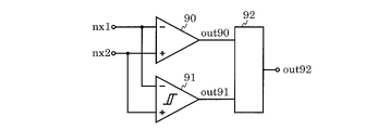
従来のゼロクロス検出回路を図12に示す。従来のゼロクロス検出回路は、比較回路90と、ヒステリシス機能を有する比較回路91と、論理回路92を備えている。比較回路90は、入力信号nx1と入力信号nx2のゼロクロス検出結果をout90端子に電圧Vout90として出力する。比較回路91は、入力信号nx1と入力信号nx2と状況によって切替えられる閾値との比較結果をout91端子に電圧Vout91として出力する。
論理回路92は、比較回路90が出力するゼロクロス検出結果Vout90と比較回路91が出力する比較結果Vout91の論理状態に応じて出力電圧Vout92の論理を決定しout92端子に出力する。
A conventional zero-cross detection circuit is shown in FIG. The conventional zero-cross detection circuit includes a
The
より詳しくは、論理回路92は、Vout91がハイレベルであるときには、Vout90のハイレベルからローレベルの遷移によってVout92をハイレベルからローレベルに遷移させる。Vout92が元々ローレベルであれば、Vout90のハイレベルからローレベルの遷移によってVout92は変化せずローレベルを維持する。Vout90のローレベルからハイレベルの遷移によってVout92は変化しない。また一方で、Vout91がローレベルであるときには、Vout90のローレベルからハイレベルの遷移によってVout92をローレベルからハイレベルに遷移させる。Vout92が元々ハイレベルであれば、Vout90のローレベルからハイレベルの遷移によってVout92は変化せずハイレベルを維持する。Vout90のローレベルからハイレベルの遷移によってVout92は変化しない。
上述のようなゼロクスロス検出回路は、ゼロクロス近傍での入力信号のノイズの影響を除去できるので、ゼロクロス点を高精度に検出することが可能である。また時間に依存しないヒステリシス特性を持たせているため、ロータの高速回転、すなわち高速な検出が可能である(例えば、特許文献1参照)。
More specifically, when the Vout 91 is at a high level, the
Since the zero cross loss detection circuit as described above can remove the influence of noise of the input signal in the vicinity of the zero cross, it is possible to detect the zero cross point with high accuracy. Further, since it has a time-independent hysteresis characteristic, high-speed rotation of the rotor, that is, high-speed detection is possible (see, for example, Patent Document 1).
しかしながら、従来のゼロクロス検出回路においては、回路に電源電圧が供給された直後の動作、すなわち動作開始時における動作に関して考慮されていなかった。例えば、モータ内のロータの回転位置を磁気センサで検出する場合においては、電源投入直後の位置検出は、ゼロクロス近傍の弱い磁場ではなく強い磁場の印加によって位置を検出することによって回転位置検出の確度を高め、回転開始時の動作を確実にしたいという要求がある。従来のゼロクロス検出回路では、このような要求に対応できないという課題があった。 However, in the conventional zero-cross detection circuit, the operation immediately after the power supply voltage is supplied to the circuit, that is, the operation at the start of the operation is not considered. For example, when the rotation position of the rotor in the motor is detected by a magnetic sensor, the position detection immediately after the power is turned on is the accuracy of the rotation position detection by detecting the position by applying a strong magnetic field instead of a weak magnetic field near the zero cross. There is a demand to increase the value and ensure the operation at the start of rotation. The conventional zero-cross detection circuit has a problem that it cannot meet such a demand.
したがって、本発明は、電源投入直後に正確な検出信号を出力することが出来るゼロクロス検出回路及びセンサ装置を提供することを目的とする。 Therefore, an object of the present invention is to provide a zero-cross detection circuit and a sensor device capable of outputting an accurate detection signal immediately after the power is turned on.
従来のこのような問題点を解決するために、本発明のゼロクロス検出回路は、入力信号n1と入力信号n2が入力され、第一比較結果を出力する第一比較回路と、ヒステリシス機能を有し、入力信号n1と入力信号n2が入力され、第二比較結果を出力する第二比較回路と、供給される電源電圧が所定の電圧以上になったときに検出信号を出力する電源電圧検出回路と、第一比較結果と第二比較結果と検出信号に基づいてゼロクロス検出信号を出力する論理回路と、を備えることを特徴とする。 In order to solve such a conventional problem, the zero cross detection circuit of the present invention has a first comparison circuit in which an input signal n1 and an input signal n2 are input and outputs a first comparison result, and a hysteresis function. , A second comparison circuit in which an input signal n1 and an input signal n2 are input and output a second comparison result, and a power supply voltage detection circuit that outputs a detection signal when the supplied power supply voltage exceeds a predetermined voltage. , A logic circuit that outputs a zero-cross detection signal based on the first comparison result, the second comparison result, and the detection signal.
本発明のゼロクスロス検出回路によれば、供給される電源電圧が所定の電圧以上になったときに論理回路に検出信号を出力する電源電圧検出回路を備えたので、電源投入直後に正確な検出信号を出力することが可能になる。 According to the zero-x loss detection circuit of the present invention, since the power supply voltage detection circuit that outputs the detection signal to the logic circuit when the supplied power supply voltage exceeds a predetermined voltage is provided, an accurate detection signal is provided immediately after the power is turned on. Can be output.
本発明のゼロクロス検出回路は、半導体回路におけるゼロクロス検出回路として幅広く利用されうる。以下、本発明のゼロクロス検出回路およびセンサ装置について図面を参照して説明する。 The zero-cross detection circuit of the present invention can be widely used as a zero-cross detection circuit in a semiconductor circuit. Hereinafter, the zero-cross detection circuit and the sensor device of the present invention will be described with reference to the drawings.
<第1の実施形態>
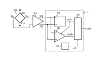
図1は、本発明の実施形態のゼロクロス検出回路を備えたセンサ装置を示すブロック図である。本実施形態のセンサ装置は、ゼロクロス検出回路1と、ホール素子2aと、差動増幅回路3aを備えている。
<First Embodiment>
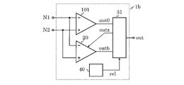
FIG. 1 is a block diagram showing a sensor device including the zero-cross detection circuit according to the embodiment of the present invention. The sensor device of this embodiment includes a zero-
ゼロクロス検出回路1は、ゼロクロス信号生成回路10と、比較回路20と、論理回路30と、電源電圧検出回路40を備えている。ゼロクロス信号生成回路10は反転入力端子と非反転入力端子と出力端子outzを有する。比較回路20は反転入力端子と非反転入力端子と閾値選択端子と出力端子outbを有する。ゼロクロス信号生成回路10の非反転入力端子と比較回路20の非反転入力端子は端子N2で共通に接続される。ゼロクロス信号生成回路10の反転入力端子と比較回路20の反転入力端子は端子N1で共通に接続される。ゼロクロス信号生成回路10の出力端子outzと比較回路20の出力端子outbは論理回路30に接続される。ゼロクロス信号生成回路10の出力端子outzは比較回路20の閾値選択端子に接続される。電源電圧検出回路40は電源端子(図示せず)と出力端子relを有する。論理回路30は出力端子outzと出力端子outbと出力端子relを入力とし、出力端子outから論理演算結果を出力する。
The zero-
ホール素子2aは、端子Aa、端子Ba、端子Ca、端子Daを有する。端子Aaと端子Caは対向した位置に配置され、端子Baと端子Daは対向した位置に配置される。端子Aaと端子Caはそれぞれ異なる電位の配線に接続される。説明のために、この異なる電位を電位VDDと、電位VDDよりも低い電位の電位VSSとし、端子Aaの電位をVDD,端子Caの電位をVSSとする。
The
差動増幅器3aは2つの入力端子と2つの出力端子を有する。2つの入力端子には、それぞれ端子Ba、端子Daが接続される。2つの出力端子は、それぞれ端子N1、端子N2に接続される。
The
以降の説明では、端子N1、端子N2、出力端子outz、出力端子outb、出力端子out、出力端子relの各電圧をそれぞれ電圧Vn1、電圧Vn2、出力電圧Voutz、出力電圧Voutb、出力電圧Vout、出力電圧Vrelとする。また、差動増幅器3a、ゼロクロス信号生成回路10、比較回路20、論理回路30および電源電圧検出回路40には電源電圧端子(図示せず)から電源電圧が供給される。説明のために、供給される電源電圧のうち、高い電位をVDD、もう一方の低い電位をVSSとし、電位VSSは0V(ゼロボルト)とすると、回路には電位VDDと電位VSS=0Vの差分である電源電圧Vddが供給される。
In the following description, the respective voltages of the terminal N1, the terminal N2, the output terminal outz, the output terminal outb, the output terminal out, and the output terminal rel are referred to as voltage Vn1, voltage Vn2, output voltage Voutz, output voltage Voutb, output voltage Vout, and output, respectively. The voltage is Vrel. Further, the power supply voltage is supplied from the power supply voltage terminal (not shown) to the
磁電変換素子であるホール素子2aの信号は、端子Baと端子Daから差動増幅器3aに入力され、差動増幅器3aはこれを増幅し、差動増幅器3aの出力はゼロクロス検出回路1の入力端子N1、入力端子N2に接続される。ここで、端子Baと端子Daの電圧をそれぞれVBa、VDaとし、ホール素子2aの信号電圧をVDa-VBaとし、差動増幅器3aの増幅率をGとする。
The signal of the
ホール素子2aの信号電圧VDa-VBaは、ホール素子2aに流れる電流の向きと、印加される磁界の向きによりフレミング左手の法則に従って、その大きさと符号が変化する。仮に紙面の手前から奥の方向に磁界が印加された場合の信号電圧VDa-VBaの符号が正とすると、紙面の奥から手前の方向に磁界が印加された場合には信号電圧VDa-VBaの符号が負となる。また、印加される磁界が大きいほど、信号電圧VDa-VBaの大きさは大きくなる。また、ホール素子2aのオフセット電圧がゼロである理想的な場合には、ホール素子2aに印加される磁界がゼロである場合の信号電圧VDa-VBaはゼロとなる。以降の説明では、ホール素子2aのオフセット電圧がゼロの場合について説明する。ホール素子2aの信号電圧は差動増幅器3aにより増幅され、
Vn2-Vn1=G×(VDa-VBa)・・・(1)
となる。従って、Vn2-Vn1はホール素子2aに印加される磁界に応じて、正または負またはゼロの値をとる。印加磁界が弱い場合にはVn2-Vn1の絶対値である|Vn2-Vn1|の値は小さく、印加磁界が強い場合には|Vn2-Vn1|の値は大きくなる。
The magnitude and sign of the signal voltage VDa-VBa of the
Vn2-Vn1 = G × (VDa-VBa) ... (1)
Will be. Therefore, Vn2-Vn1 takes a positive, negative, or zero value depending on the magnetic field applied to the
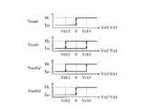
ゼロクロス検出回路1は、端子N1および端子N2に入力される電圧Vn2、Vn1に応じて出力電圧Voutを変化させる。この動作を図2および図3~図6を用いて説明する。
The zero-
先ず、ゼロクロス信号生成回路10の動作を説明する。ゼロクロス信号生成回路10は非反転入力端子に供給される電圧が反転入力端子に供給される電圧よりも高いときは出力端子outzからハイレベルを出力し、これとは逆に、非反転入力端子に供給される電圧が反転入力端子に供給される電圧よりも低いときは、出力端子outzからローレベルを出力するように動作する。この動作の詳細を図2に示す。
First, the operation of the zero-cross
図2の横軸は電圧Vn1と電圧Vn2の入力電圧差を示し、縦軸は各々の出力電圧を示す。出力電圧Voutzは、電圧Vn2が電圧Vn1よりも高いとき、すなわち、Vn2-Vn1>0であるときはハイレベルを出力する。これとは逆に、電圧Vn2が電圧Vn1よりも低いとき、すなわち、Vn2-Vn1<0であるときはローレベルを出力する。従って、ゼロクロス信号生成回路10は入力される電圧Vn2と電圧Vn1の差分に応じた出力電圧Voutzを出力する。ここで、出力電圧Voutzはゼロクロス近傍、すなわちVn2-Vn1=0近傍のノイズを除去した信号である。このノイズ除去動作の例については後述する。
The horizontal axis of FIG. 2 shows the input voltage difference between the voltage Vn1 and the voltage Vn2, and the vertical axis shows the respective output voltages. The output voltage Voutz outputs a high level when the voltage Vn2 is higher than the voltage Vn1, that is, when Vn2-Vn1> 0. On the contrary, when the voltage Vn2 is lower than the voltage Vn1, that is, when Vn2-Vn1 <0, a low level is output. Therefore, the zero-cross
次に、比較回路20の動作を説明する。比較回路20は、非反転入力端子に供給される電圧が反転入力端子に供給される電圧と電圧Vth1の和よりも高いときは出力端子outbからハイレベルを出力し、これとは逆に、非反転入力端子に供給される電圧が反転入力端子に供給される電圧と電圧Vth2の和よりも低いときは、出力端子outbからローレベルを出力するように動作する。電圧Vth1と電圧Vth2のどちらが選択されるかは、出力電圧Voutzにより決定される。出力電圧Voutzがハイレベルのときは電圧Vth1が選択され、出力電圧Voutzがローレベルのときは電圧Vth2が選択される。この動作の詳細を図2に示す。出力電圧Voutbは、電圧Vn2が電圧Vn1と電圧Vth1の和よりも高いとき、すなわち、Vn2-Vn1>Vth1であるときはハイレベルを出力し、電圧Vn2が電圧Vn1と電圧Vth2の和よりも低いとき、すなわち、Vn2-Vn1<Vth2であるときはローレベルを出力する。ここで、電圧Vth1は正の値でプラス側の閾値電圧を表し、電圧Vth2は負の値でマイナス側の閾値電圧を表す。出力電圧Voutbは、Vn2-Vn1がVth1とVth2の間であるとき、すなわち、Vth2<Vn2-Vn1<Vth1であるときは選択された閾値電圧に応じてハイレベルまたはローレベルを出力する。
Next, the operation of the
次に、電源電圧検出回路40の動作を説明する。電源電圧検出回路40は、供給される電源電圧に応じて出力電圧Vrelを変化させる。出力電圧Vrelは、供給される電源電圧が低いときはローレベルを出力し、回路動作が正常に行われる十分な電圧が供給された場合にはハイレベルを出力する。
Next, the operation of the power supply
次に、論理回路30の動作を説明する。論理回路30は出力電圧Voutzと出力電圧Voutbと出力電圧Vrelの論理状態に応じて出力電圧Voutの論理を決定するように動作する。出力電圧Vrelがローレベルからハイレベルに遷移した直後は、論理回路30は比較回路20の出力電圧Voutbにもとづいて決定された電圧をVoutに出力する。その後、すなわち比較回路20の出力電圧Voutbにもとづいて決定された電圧をVoutに出力した後は、論理回路30はゼロクロス信号生成回路10の出力電圧Voutzにもとづいて決定された電圧をVoutに出力するように動作する。出力電圧Vrelがローレベルからハイレベルに遷移した直後の動作の詳細を図2の波形Vout(a)に示し、その後の動作の詳細を波形Vout(b)に示す。また、この動作の詳細について図3~図6を用いて説明する。
Next, the operation of the
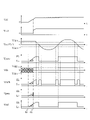
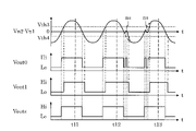
図3は、十分に強い正の信号、すなわちVn2-Vn1>Vth1であるときに電源が投入された場合のゼロクロス検出回路1の動作を示す図である。ここで横軸は時間経過を示し、縦軸は入力電圧差または出力電圧を示す。
FIG. 3 is a diagram showing the operation of the zero
回路に供給される電源電圧Vddは、時刻t0において0V(ゼロボルト)から上昇を開始し、時刻t1で回路が正常に動作するのに十分な電圧に達する。電源電圧検出回路40の出力電圧Vrelは、回路が正常に動作するのに十分な電源電圧Vddに達したことを受けて、時刻t1でローレベルからハイレベルに変化する。
The power supply voltage Vdd supplied to the circuit starts to rise from 0V (zero volt) at time t0 and reaches a voltage sufficient for the circuit to operate normally at time t1. The output voltage Vrel of the power supply
時刻t1より前の時刻においては、回路に供給される電源電圧Vddが低いために、ゼロクロス信号生成回路10および比較回路20は正常または正確に動作せず、出力電圧VoutzおよびVoutbは入力電圧に応じた出力電圧が得られない可能性がある。また出力電圧Voutについても同様に入力電圧に応じたVoutが得られない可能性がある。これを図3では斜線で示している。また、電源電圧Vddが低いときには、出力電圧Voutz、VoutbおよびVoutを強制的にローレベルまたはハイレベルにしても良い。出力電圧VoutzおよびVoutbの出力を強制的にローレベルまたはハイレベルにする動作は、ゼロクロス信号生成回路10および比較回路20に電源電圧検出回路40の出力Vrelを接続することによって実現できる(図示せず)。図3では、出力電圧Vrelがローレベルの場合には、出力電圧Voutzを強制的にローレベルにして、出力電圧VoutbおよびVoutハイレベルにした場合を示している。
At times before time t1, the zero-cross
時刻t1より後の時刻においては、電源電圧Vddは回路が正常に動作するのに十分な電源電圧に達しているため、ゼロクロス信号生成回路10および比較回路20は正常かつ正確に動作しているとみなすことができる。従って出力電圧VoutzおよびVoutbについても入力電圧Vn2およびVn1に正しく応じた出力電圧であると見なすことができる。
At a time after time t1, the power supply voltage Vdd has reached a power supply voltage sufficient for the circuit to operate normally, so that the zero-cross
時刻t1の直後の時刻において、ゼロクロス信号生成回路10の出力電圧Voutzは、Vn2-Vn1>0であるからハイレベルを出力する。従って、比較回路20の閾値電圧Vthは電圧Vth1が選択される。Vn2-Vn1>Vth1であるから、比較回路20の出力電圧Voutbはハイレベルを出力する。論理回路30は出力電圧Voutzおよび出力電圧Voutbがハイレベルであり、同じレベルであることから、十分に大きい信号が入力されていると判断し、論理回路30は比較回路20の出力電圧Voutbにもとづいて決定された電圧、すなわちハイレベルを出力電圧Voutに出力する。電圧Vponは、論理回路30の内部信号であり回路図中には図示していない。電圧Vponは、論理回路30が比較回路20の出力電圧Voutbにもとづいて決定された電圧を出力する前にハイレベルとなり、論理回路30が比較回路20の出力電圧Voutbにもとづいて決定された電圧を出力した後にローレベルとなる信号である。一例としては、出力電圧Vrelがハイレベルになった際に電圧Vponがセットされてハイレベルになり、出力電圧VoutzとVoutbが同じレベルになった際に電圧Vponがリセットされてローレベルになるように構成される。論理回路30は、電圧Vopnがハイレベルのときには出力電圧Voutbにもとづいて決定された電圧を電圧Voutに出力し、電圧Vopnがローレベルのときには出力電圧Voutzにもとづいて決定された電圧を電圧Voutに出力する。本場合においては、上述のとおり時刻t1の直後の時刻において、出力電圧Voutには出力電圧Voutbにもとづいた電圧が出力されて、電圧Vponはハイレベルからローレベルに遷移する。従って、これ以降の時刻では、論理回路30はゼロクロス信号生成回路10の出力電圧Voutzにもとづいて決定された電圧をVoutに出力するように動作する。
At the time immediately after the time t1, the output voltage Voutz of the zero-cross
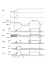
図4は、弱い正の信号、すなわち0<Vn2-Vn1<Vth1であるときに電源が投入された場合のゼロクロス検出回路1の動作を示す図である。電源電圧Vddおよび出力電圧Vrelの波形については図3と同様であり、斜線部についても図3と同様である。時刻t1までの時刻においてのVoutz、Voutb、VponおよびVoutの波形についても図3と同様である。
FIG. 4 is a diagram showing the operation of the zero
時刻t1の直後の時刻において、ゼロクロス信号生成回路10の出力電圧Voutzは、Vn2-Vn1>0であるからハイレベルを出力する。従って、比較回路20の閾値電圧Vthは電圧Vth1が選択される。Vn2-Vn1<Vth1であるから、比較回路20の出力電圧Voutbはローレベルを出力する。論理回路30は、出力電圧Voutzがハイレベル、出力電圧Voutbがローレベルであり、異なるレベルであることから、小さい信号が入力されていると判断し、論理回路30は出力電圧Voutを変更せず、直前の電圧であるハイレベルを保持する。電圧Vponについてもハイレベルを保持する。
At the time immediately after the time t1, the output voltage Voutz of the zero-cross
時刻t1より後の時刻に、Vn2-Vn1は変化を開始し、時刻t2でVn2-Vn1=0となる。すなわちゼロクロスする。時刻t2の直後の時刻に、ゼロクロス信号生成回路10の出力電圧Voutzは、Vn2-Vn1<0であるからローレベルを出力する。従って、比較回路20の閾値電圧Vthは電圧Vth2が選択される。Vn2-Vn1>Vth2であるから、比較回路20の出力電圧Voutbはハイレベルを出力する。論理回路30は、出力電圧Voutzがローレベル、出力電圧Voutbがハイレベルであり、異なるレベルであることから、小さい信号が入力されていると判断し、論理回路30は出力電圧Voutを変更せず、直前の電圧であるハイレベルを保持する。電圧Vponについてもハイレベルを保持する。
At a time after the time t1, Vn2-Vn1 starts changing, and at the time t2, Vn2-Vn1 = 0. That is, zero cross. At the time immediately after the time t2, the output voltage Voutz of the zero cross
時刻t2より後の時刻でもVn2-Vn1は変化を続け、時刻t3でVn2-Vn1=Vth2となる。時刻t3の直後の時刻に、Vn2-Vn1<Vth2となり、比較回路20の出力電圧Voutbはローレベルを出力する。論理回路30は出力電圧Voutzおよび出力電圧Voutbがローレベルであり、同じレベルであることから、十分に大きい信号が入力されていると判断し、論理回路30は比較回路20の出力電圧Voutbにもとづいて決定された電圧、すなわちローレベルを出力電圧Voutに出力する。電圧Vponはハイレベルからローレベルに遷移する。これ以降の時刻では、論理回路30はゼロクロス信号生成回路10の出力電圧Voutzにもとづいて決定された電圧をVoutに出力するように動作する。
Vn2-Vn1 continues to change even at a time after the time t2, and Vn2-Vn1 = Vth2 at the time t3. At the time immediately after the time t3, Vn2-Vn1 <Vth2, and the output voltage Voutb of the
図5は、弱い負の信号、すなわちVth2<Vn2-Vn1<0であるときに電源が投入された場合のゼロクロス検出回路1の動作を示す図である。電源電圧Vddおよび出力電圧Vrelの波形については図3と同様であり、斜線部についても図3と同様である。時刻t1までの時刻においてのVoutz、Voutb、VponおよびVoutの波形についても図3と同様である。
FIG. 5 is a diagram showing the operation of the zero
時刻t1の直後の時刻において、ゼロクロス信号生成回路10の出力電圧Voutzは、Vn2-Vn1<0であるからローレベルを出力する。従って、比較回路20の閾値電圧Vthは電圧Vth2が選択される。Vn2-Vn1>Vth2であるから、比較回路20の出力電圧Voutbはハイレベルを出力する。論理回路30は、出力電圧Voutzがローレベル、出力電圧Voutbがハイレベルであり、異なるレベルであることから、小さい信号が入力されていると判断し、論理回路30は出力電圧Voutを変更せず、直前の電圧であるハイレベルを保持する。電圧Vponについてもハイレベルを保持する。
At the time immediately after the time t1, the output voltage Voutz of the zero-cross
時刻t1より後の時刻に、Vn2-Vn1は変化を開始し、時刻t3でVn2-Vn1=Vth2となる。時刻t3の直後の時刻に、Vn2-Vn1<Vth2となり、比較回路20の出力電圧Voutbはローレベルを出力する。論理回路30は出力電圧Voutzおよび出力電圧Voutbがローレベルであり、同じレベルであることから、十分に大きい信号が入力されていると判断し、論理回路30は比較回路20の出力電圧Voutbにもとづいて決定された電圧、すなわちローレベルを出力電圧Voutに出力する。電圧Vponはハイレベルからローレベルに遷移する。これ以降の時刻では、論理回路30はゼロクロス信号生成回路10の出力電圧Voutzにもとづいて決定された電圧をVoutに出力するように動作する。
At a time after the time t1, Vn2-Vn1 starts changing, and at the time t3, Vn2-Vn1 = Vth2. At the time immediately after the time t3, Vn2-Vn1 <Vth2, and the output voltage Voutb of the
図6は、十分に強い負の信号、すなわちVn2-Vn1<Vth2であるときに電源が投入された場合のゼロクロス検出回路1の動作を示す図である。電源電圧Vddおよび出力電圧Vrelの波形については図3と同様であり、斜線部についても図3と同様である。時刻t1までの時刻においてのVoutz、Voutb、VponおよびVoutの波形についても図3と同様である。
FIG. 6 is a diagram showing the operation of the zero
時刻t1の直後の時刻において、ゼロクロス信号生成回路10の出力電圧Voutzは、Vn2-Vn1<0であるからローレベルを出力する。従って、比較回路20の閾値電圧Vthは電圧Vth2が選択される。Vn2-Vn1<Vth2であるから、比較回路20の出力電圧Voutbはローレベルを出力する。論理回路30は、出力電圧Voutzおよび出力電圧Voutbがローレベルであり、同じレベルであることから、十分に大きい信号が入力されていると判断し、論理回路30は比較回路20の出力電圧Voutbにもとづいて決定された電圧、すなわちローレベルを出力電圧Voutに出力する。電圧Vponはハイレベルからローレベルに遷移する。これ以降の時刻では、論理回路30はゼロクロス信号生成回路10の出力電圧Voutzにもとづいて決定された電圧をVoutに出力するように動作する。
At the time immediately after the time t1, the output voltage Voutz of the zero-cross
次に、ゼロクロス信号生成回路10のノイズ除去動作の一例について説明する。
図7は、第1の実施形態のゼロクロス信号生成回路10の一例の回路図である。
Next, an example of the noise reduction operation of the zero-cross
FIG. 7 is a circuit diagram of an example of the zero-cross
ゼロクロス信号生成回路10は、比較回路101と比較回路102と論理回路103で構成されている。比較回路101は反転入力端子と非反転入力端子と出力端子out0を有する。比較回路102は反転入力端子と非反転入力端子と出力端子out1を有する。比較回路101の反転入力端子と比較回路102の反転入力端子は端子N1で共通に接続される。比較回路101の非反転入力端子と比較回路102の非反転入力端子は端子N2で共通に接続される。端子N1と端子N2には、それぞれ第一入力信号と第二入力信号が供給される。比較回路101の出力端子out0と比較回路102の出力端子out1は論理回路103に接続される。論理回路103は出力端子out0と出力端子out1を入力とし、出力端子outzから論理演算結果を出力する。以降の説明では、出力端子out0、出力端子out1の各電圧をそれぞれ出力電圧Vout0、出力電圧Vout1とする。
The zero-cross
次に、ゼロクロス信号生成回路10の動作を図8および図9を用いて説明する。
まず、比較回路101の動作を説明する。比較回路101は、非反転入力端子に供給される電圧が反転入力端子に供給される電圧よりも高いときは出力端子out0からハイレベルを出力し、これとは逆に、非反転入力端子に供給される電圧が反転入力端子に供給される電圧よりも低いときは、出力端子out0からローレベルを出力するように動作する。この動作の詳細を図8に示す。ここで横軸は電圧Vn1とVn2の入力電圧差を示し、縦軸は各々の出力電圧を示す。図8に示すように、出力電圧Vout0は、電圧Vn2が電圧Vn1よりも高いとき、すなわち、Vn2-Vn1>0であるときはハイレベルを出力する。これとは逆に、電圧Vn2が電圧Vn1よりも低いとき、すなわち、Vn2-Vn1<0であるときはローレベルを出力する。出力電圧Vout0のハイレベルからローレベルへの遷移は、Vn2-Vn1=0で行われる。また、出力電圧Vout0のローレベルからハイレベルへの遷移は、同様にVn2-Vn1=0で行われる。
Next, the operation of the zero-cross
First, the operation of the
また、入力電圧差Vn2-Vn1が時間変化した場合の比較回路101の動作を図9に示す。ここで横軸は時間経過を示し、縦軸は入力電圧差または出力電圧を示す。入力電圧差Vn2-Vn1は時間変化に伴って変化し、様々な値を取りうる。特に、Vn2-Vn1=0となるときをゼロクロスと表現している。入力電圧差Vn2-Vn1の時間変化に伴って、出力電圧Vout0は変化する。出力電圧Vout0は、Vn2-Vn1>0のときはハイレベルを出力し、Vn2-Vn1<0のときはローレベルを出力する。Vn2-Vn1=0のとき、すなわち、Vn1=Vn2のときに出力電圧Vout0はゼロクロス検出する。
Further, FIG. 9 shows the operation of the
次に、比較回路102の動作を説明する。比較回路102は、非反転入力端子に供給される電圧が反転入力端子に供給される電圧と電圧Vth3の和よりも高いときは出力端子out1からハイレベルを出力し、これとは逆に、非反転入力端子に供給される電圧が反転入力端子に供給される電圧と電圧Vth4の和よりも低いときは、出力端子out1からローレベルを出力するように動作する。この動作の詳細を図8に示す。図8に示すように、出力電圧Vout1は、電圧Vn2が電圧Vn1と電圧Vth3の和よりも高いとき、すなわち、Vn2-Vn1>Vth3であるときはハイレベルを出力し、電圧Vn2が電圧Vn1と電圧Vth4の和よりも低いとき、すなわち、Vn2-Vn1<Vth4であるときはローレベルを出力する。ここで、電圧Vth3は正の値でプラス側のヒステリシス値を表し、電圧Vth4は負の値でマイナス側のヒステリシス値を表す。出力電圧Vout1のハイレベルからローレベルへの遷移は、Vn2-Vn1=Vth4で行われる。また、出力電圧Vout1のローレベルからハイレベルへの遷移は、Vn2-Vn1=Vth3で行われる。Vn2-Vn1がVth3とVth4の間であるときには、直前の状態に応じてハイレベルまたはローレベルを出力する。すなわち、比較回路102は、ヒステリシス幅|Vth3|+|Vth4|を有する比較回路として動作する。
Next, the operation of the
また、入力電圧差Vn2-Vn1が時間変化した場合の比較回路102の動作を図9に示す。入力電圧差Vn2-Vn1の時間変化に伴って出力電圧Vout1は変化する。時刻t11のとき、すなわちVn2-Vn1>Vth3のときに出力電圧Vout1はハイレベルを出力し、その後の時間経過後もハイレベルを維持し、Vn2-Vn1の減少に伴い、Vn2-Vn1<Vth4となったときにハイレベルからローレベルの出力に遷移し、その後の時間経過後もローレベルを維持し、Vn2-Vn1の増加に伴い、Vn2-Vn1>Vth3となったときにローレベルからハイレベルに遷移する。
Further, FIG. 9 shows the operation of the
次に、論理回路103の動作を説明する。論理回路103は、出力電圧Vout0と出力電圧Vout1の論理状態に応じて出力電圧Voutzの論理を決定するように動作する。より詳しくは、論理回路103は、Vout1がハイレベルであるときには、Vout0のハイレベルからローレベルの遷移によってVoutzをハイレベルからローレベルに遷移させる。Voutzが元々ローレベルであればVoutzは変化しない。Vout0のローレベルからハイレベルの遷移によってVoutzは変化しない。また、Vout1がローレベルであるときには、Vout0のローレベルからハイレベルの遷移によってVoutzをローレベルからハイレベルに遷移させる。Voutzが元々ハイレベルであればVoutzは変化しない。Vout0のハイレベルからローレベルの遷移によってVoutzは変化しない。以上の動作について図9を用いて説明する。
Next, the operation of the
図9において、時刻t11のとき、出力電圧Vout0と出力電圧Vout1はハイレベルである。その後、時間が経過してVn2-Vn1が減少し、ゼロクロスしたときにVout0はハイレベルからローレベルに遷移する。このとき、Vout1はハイレベルであるから、論理回路103は、Vout0のハイレベルからローレベルのゼロクロスの検出をVoutzに出力する。その後、時間が経過し、Vn2-Vn1<Vth4となると、Vout1はハイレベルからローレベルに遷移する。その後、時間が経過してVn2-Vn1が増加し、ゼロクロスしたときにVout0はローレベルからハイレベルに遷移する。このとき、Vout1はローレベルであるから、論理回路103は、Vout0のローレベルからハイレベルのゼロクロスの検出をVoutzに出力する。その後、時間が経過し、Vn2-Vn1>Vth3となると、Vout1はローレベルからハイレベルに遷移する。さらにその後、時間が経過し時刻t12のときには、時刻t11と同じ状態になる。
In FIG. 9, at time t11, the output voltage Vout0 and the output voltage Vout1 are at high levels. After that, Vn2-Vn1 decreases with the passage of time, and when zero crossing occurs, Vout0 transitions from a high level to a low level. At this time, since Vout1 is at a high level, the
時刻t12のとき、出力電圧Vout0と出力電圧Vout1はハイレベルである。その後、時間が経過してVn2-Vn1が減少し、ゼロクロスしたときにVout0はハイレベルからローレベルに遷移する。このとき、Vout1はハイレベルであるから、論理回路103は、Vout0のハイレベルからローレベルのゼロクロスの検出をVoutzに出力する。その後、時間が経過し、ノイズnsによってVn2-Vn1は2回ゼロクロスし、出力電圧Vout0は、ローレベルからハイレベルに遷移した後、さらにローレベルに遷移する。このとき、Vout1はハイレベルであるから、論理回路103はVout0のローレベルからハイレベルの遷移をVoutzに出力しないように動作する。従って、ノイズによるゼロクロス検出は出力端子outzには現れない。さらに時間が経過し、Vn2-Vn1<Vth4となると、Vout1はハイレベルからローレベルに遷移する。その後、時間が経過してVn2-Vn1が増加し、ゼロクロスしたときにVout0はローレベルからハイレベルに遷移する。このとき、Vout1はローレベルであるから、論理回路103は、Vout0のローレベルからハイレベルのゼロクロスの検出をVoutに出力する。その後、時間が経過し、ノイズnsによってVn2-Vn1は2回ゼロクロスし、出力電圧Vout0は、ハイレベルからローレベルに遷移した後、さらにハイレベルに遷移する。このとき、Vout1はローレベルであるから、Vout0のハイレベルからローレベルの遷移をVoutzに出力しないように動作する。従って、ノイズによるゼロクロス検出は出力端子outzには現れない。その後、時間が経過し、Vn2-Vn1>Vth3となると、Vout1はローレベルからハイレベルに遷移する。さらにその後、時間が経過し時刻t13のときには、時刻t11および時刻12と同じ状態になる。
At time t12, the output voltage Vout0 and the output voltage Vout1 are at high levels. After that, Vn2-Vn1 decreases with the passage of time, and when zero crossing occurs, Vout0 transitions from a high level to a low level. At this time, since Vout1 is at a high level, the
以上により、ゼロクロス信号生成回路10の動作を説明し、ゼロクロス検出を行うと共に、ノイズによるゼロクロスの影響を除去することができ、高精度なゼロクロス信号を簡便な回路構成にて得ることが可能であることを示した。
With the above, the operation of the zero-cross
ゼロクロス信号生成回路10の動作について、本説明においては、電圧Vth3と電圧Vth4を比較回路102のヒステリシス電圧として説明したが、比較回路102の機能を2つの、比較回路に分割し、一方の比較回路でVn2-Vn1が電圧Vth3より大きいか小さいかを判別し、もう一方の比較回路でVn2-Vn1が電圧Vth4より大きいか小さいかを判別するようにしてもよい。
Regarding the operation of the zero-cross
以上により、本発明の実施形態のゼロクロス検出回路を備えたセンサ装置の動作を説明し、ゼロクロス検出を行うと共に、電源電圧が供給された直後、すなわち動作開始時においては、入力信号の大小をより確実に検出できることを示した。すなわち、本発明のゼロクロス検出回路の動作により、ホール素子2aに印加される磁界のゼロクロス点を検出可能であり、かつ、動作開始時の磁界の大小をより確実に検出可能であることを示した。別の表現をすると、本発明のゼロクロス検出回路を搭載したセンサ装置と磁石との相対的な位置関係を検出する用途において、相対位置の変化によってセンサ装置に印加される磁界がS極からN極に切り替わる点、またはN極からS極に切り替わる点を高精度に検出することが可能であり、かつ、動作開始時の相対位置をより確実に検出可能である。従って本発明のゼロクロス検出回路は、ロータの回転位置を高精度に検出する必要があるブラシレスモータでの使用やエンコーダでの使用に好適である。本実施形態のゼロクロス検出回路を備えたセンサ装置をブラシレスモータで使用すれば、ゼロクロス検知による回転性能の向上だけでなく、強い磁場の印加によって電源投入直後の回転位置検出の確度を高めることができ、回転開始時の動作を確実にすることが可能となる。
The operation of the sensor device provided with the zero-cross detection circuit according to the embodiment of the present invention will be described above, and the magnitude of the input signal will be determined immediately after the power supply voltage is supplied, that is, at the start of operation, while performing zero-cross detection. It was shown that it can be detected reliably. That is, it was shown that the zero cross point of the magnetic field applied to the
本説明においては、説明のために詳細な条件を記載して説明したが、本発明の趣旨に沿う動作および回路構成であれば、この限りではない。例えば、各電圧のハイレベルとローレベルを明示したが、それぞれハイレベルとローレベルは逆でも良く、またハイレベルとローレベルの組合せは異なっても良い。また、回路動作が正常に行われる十分な電圧に達してから出力電圧Vrelが変化するまでの時間については特に言及せず説明したが、遅延時間を設けても良い。
また、電圧Vth3と電圧Vth4は、それぞれ電圧Vth1と電圧Vth2と等しい電圧でも良い。また、比較回路20の閾値Vthを制御する信号をゼロクロス信号生成回路10の出力電圧Voutzとしたが、この限りではなく、論理回路30内で生成する出力電圧Voutzにもとづく電圧により制御しても良い。また、比較回路20の閾値Vthを外部から制御するのではなく、比較回路102と同様に自らの出力によって閾値を制御する構成としてもよい。さらに、電圧Vponは出力電圧Voutzと出力電圧Voutbが同じレベルになった際にローレベルになるように構成を説明したが、出力電圧Voutが出力電圧Voutbにもとづいて出力されたことと同義の信号である構成であればこの限りではない。例えば、出力電圧Voutは、出力電圧Voutzと出力電圧Voutbの論理和であっても良い。
In this description, detailed conditions have been described and described for the sake of explanation, but the present invention is not limited to this as long as the operation and circuit configuration are in line with the gist of the present invention. For example, although the high level and low level of each voltage are specified, the high level and low level may be reversed, and the combination of high level and low level may be different. Further, although the time from reaching a sufficient voltage at which the circuit operation is normally performed until the output voltage Vrel changes has been described without particular reference, a delay time may be provided.
Further, the voltage Vth3 and the voltage Vth4 may be the same as the voltage Vth1 and the voltage Vth2, respectively. Further, the signal for controlling the threshold Vth of the
<第2の実施形態>
図10は、本発明の第2の実施形態のゼロクロス検出回路を示すブロック図である。図10に示すゼロクロス検出回路1bと、図1に示したゼロクロス検出回路1との違いは、ゼロクロス信号生成回路10を削除し、ゼロクロス信号生成回路10内の比較回路101を追加し、論理回路30を削除し、論理回路31を追加した点である。追加した要素は次のように構成され、接続される。また削除した要素により次の接続および動作が図1に示したゼロクロス検出回路1と異なる。図1および図7の場合と同様に、比較回路101の反転入力端子は端子N1に接続され、非反転入力端子は端子N2で共通に接続される。比較回路101の出力端子out0は、図1および図7の場合と異なり、論理回路31に接続される。論理回路31は、論理回路30の機能に論理回路103の機能を統合した機能を備え、具体的には出力電圧Vout0と出力電圧Voutbから出力信号Voutzを生成する機能を追加で備える。また、論理回路31は出力電圧Voutzと出力電圧Voutbと出力電圧Vrelの論理状態に応じて出力電圧Voutの論理を決定するように動作する。出力電圧Vrelがローレベルからハイレベルに遷移した直後は、論理回路31は比較回路20の出力電圧Voutbにもとづいて決定された電圧をVoutに出力する。その後、すなわち比較回路20の出力電圧Voutbにもとづいて決定された電圧をVoutに出力し、出力電圧Vrelがハイレベルからローレベルに遷移した後は、比較回路20は出力信号Voutzにより図7の比較回路102と同様の動作をするように制御され、さらに、論理回路31は、出力信号Vout0と出力信号Voutbから出力電圧Voutzを生成し、出力電圧Voutzを生成にもとづいて決定された電圧をVoutに出力するように動作する。
<Second embodiment>
FIG. 10 is a block diagram showing a zero-cross detection circuit according to a second embodiment of the present invention. The difference between the zero-
以上のように構成し、動作させることで本実施例のゼロクロス検出回路1bは第1の実施形態のゼロクロス検出回路1と同様の出力電圧Voutを得ることができ、比較回路102を削除することにより回路規模の縮小を実現できる。
By configuring and operating as described above, the zero-
<第3の実施形態>
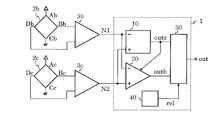
図11は、本発明の実施形態のゼロクロス検出回路を備えた磁気センサ装置の他の例を示すブロック図である。
ホール素子2bと差動増幅回路3bの接続の構成は、図1の磁気センサ装置のホール素子2aと差動増幅回路3aの接続の構成と同様である。またホール素子2cと差動増幅回路3cの接続の構成も、図1のホール素子2aと差動増幅回路3aの接続の構成と同様である。差動増幅回路3bおよび3cは差動増幅回路3aが差動出力であるのに対して、シングルエンドで出力する。磁電変換素子であるホール素子2bの信号は、端子Bbと端子Dbから差動増幅器3bに入力され、差動増幅器3bはこれを増幅し、差動増幅器3bの出力は本発明のゼロクロス検出回路1の端子N1に接続される。また、磁電変換素子であるホール素子2cの信号は、端子Bcと端子Dcから差動増幅器3cに入力され、差動増幅器3cはこれを増幅し、差動増幅器3cの出力は本発明のゼロクロス検出回路1の端子N2に接続される。
<Third embodiment>
FIG. 11 is a block diagram showing another example of the magnetic sensor device including the zero-cross detection circuit according to the embodiment of the present invention.
The configuration of the connection between the
ここで、端子Bb、Db、Bc、Dcの各電圧をそれぞれVBb、VDb、VBc、VDcとし、ホール素子2bおよび2cの信号電圧をそれぞれVDb-VBb、VDc-VBcとし、差動増幅器3bおよび3cの増幅率をともにGとする。すると、端子N1に供給される電圧Vn1と端子N2に供給される電圧Vn2は次のようになる。
Vn1=G×(VDb-VBb)・・・(2)
Vn2=G×(VDc-VBc)・・・(3)
式(2)と式(3)から次式を得る。
Vn2-Vn1=G×{(VDc-VBc)-(VDb-VBb)}・・・(4)
従って、Vn2-Vn1はホール素子2bとホール素子2cに印加される磁界に応じて、正または負またはゼロの値をとる。すなわち、本発明のゼロクロス検出回路1の動作により、ホール素子2bとホール素子2cに印加される磁界の差のゼロクロス点を検出可能であり、かつ、動作開始時においては入力信号の大小をより確実に検出することが可能になる。別の表現をすると、2つのセンサ素子の信号が等しい場合にはゼロクロス検出信号を出力し、2つのセンサ素子のどちらの信号が大きいかを弁別して出力することが可能になり、かつ、動作開始時においては、どちらの信号が大きいかをより確実に検出することが可能になる。本実施例は、例えば、バイアス磁界を発生する磁石と、鉄などの金属や磁性体で構成された歯車の間に磁気センサ装置を配置し、歯車の回転を磁気センサ装置で検出する用途で好適である。
Here, the voltages of the terminals Bb, Db, Bc, and Dc are set to VBb, VDb, VBc, and VDc, respectively, and the signal voltages of the
Vn1 = G × (VDb-VBb) ... (2)
Vn2 = G × (VDc-VBc) ... (3)
The following equations are obtained from equations (2) and (3).
Vn2-Vn1 = G × {(VDc-VBc)-(VDb-VBb)} ... (4)
Therefore, Vn2-Vn1 takes a positive, negative, or zero value depending on the magnetic fields applied to the
本説明では、説明の便宜上、差動増幅回路3bおよび3cはシングルエンドで出力するとしたが、ノイズ耐性の向上を図るために差動出力としても良い。また、ホール素子が2つの場合を説明したが、2つより多くても良い。例えば、2つのホール素子の差分信号1と、これとは別の2つのホール素子の差分信号2を生成し、差分信号1と差分信号2のゼロクロスを検出するようにしても良い。
In this description, for convenience of explanation, the
図1および図11に本発明のゼロクロス検出回路を備えたセンサ装置の例を示した。本説明においては、説明のために具体的な例を示したが、必ずしもこの構成やセンサ素子に制限されるものではなく、広範な半導体回路およびセンサ回路において応用可能である。一例としては、磁電変換素子であるホール素子の非理想成分であるオフセット電圧をキャンセルするスピニングカレント回路と組み合わせてもよく、また差動増幅器や比較回路の非理想成分であるオフセット電圧をキャンセルするチョッピング動作またはオートゼロ動作の回路等と組み合わせてもよい。ここで、スピニングカレント回路やチョッピング動作またはオートゼロ動作の回路等と組み合せた場合は、連続時間の信号処理ではなく離散時間の信号処理となるため、ゼロクロス信号生成回路10、比較回路20、101、102のそれぞれの出力を組み合わせ回路によって演算して出力端子outから出力するのは好ましくない。この場合はラッチ回路等の順序回路と組み合わせるのが好適である。また磁電変換素子以外にも、温度センサ素子、加速度センサ素子、圧力センサ素子といったセンサ素子のゼロクロス検出回路としても良い。
1 and 11 show an example of a sensor device including the zero-cross detection circuit of the present invention. In this description, a specific example is shown for the sake of explanation, but the present invention is not necessarily limited to this configuration or sensor element, and can be applied to a wide range of semiconductor circuits and sensor circuits. As an example, it may be combined with a spinning current circuit that cancels an offset voltage that is a non-ideal component of a Hall element that is a magnetic-electric conversion element, and chopping that cancels an offset voltage that is a non-ideal component of a differential amplifier or a comparison circuit. It may be combined with a circuit of operation or auto-zero operation. Here, when combined with a spinning current circuit, a chopping operation, an auto-zero operation circuit, or the like, the signal processing is not continuous time but discrete time, so that the zero cross
1、1b ゼロクロス検出回路
10 ゼロクロス信号生成回路
20、101、102 比較回路
30、31、103 論理回路
40 電源電圧検出回路
2a、2b、2c ホール素子
3a、3b、3c 差動増幅回路
1,1b Zero-
Claims (3)
ヒステリシス機能を有し、前記入力信号n1と前記入力信号n2が入力され、第二比較結果を出力する第二比較回路と、
供給される電源電圧が所定の電圧以上になったときに検出信号を出力する電源電圧検出回路と、
前記第一比較結果と前記第二比較結果と前記検出信号に基づいてゼロクロス検出信号を出力する論理回路と、を備え
前記第二比較回路は、第一閾値及び第二閾値と、前記第一比較結果が入力される閾値選択端子とを有し、
前記第一比較結果に応じて前記第一閾値と前記第二閾値を切替える
ことを特徴とするゼロクロス検出回路。 An input signal n1 and an input signal n2, which are output signals of the sensor element, are input, and a first comparison circuit that outputs the first comparison result,
A second comparison circuit having a hysteresis function, the input signal n1 and the input signal n2 being input, and the second comparison result being output.
A power supply voltage detection circuit that outputs a detection signal when the supplied power supply voltage exceeds a predetermined voltage,
A logic circuit that outputs a zero-cross detection signal based on the first comparison result, the second comparison result, and the detection signal is provided .
The second comparison circuit has a first threshold value and a second threshold value, and a threshold value selection terminal into which the first comparison result is input.
The first threshold value and the second threshold value are switched according to the first comparison result.
A zero-cross detection circuit characterized by this.
前記第一比較結果と前記第二比較結果が同じレベルであると、前記第二比較結果に基づいて決定される前記ゼロクロス検出信号を出力し、
前記第一比較結果と前記第二比較結果が異なったレベルであると、前記第一比較結果と前記第二比較結果に基づいて決定される前記ゼロクロス検出信号を出力する
ことを特徴とする請求項1に記載のゼロクロス検出回路。 When the logic circuit receives the detection signal, the logic circuit receives the detection signal.
When the first comparison result and the second comparison result are at the same level, the zero cross detection signal determined based on the second comparison result is output.
The claim is characterized in that when the first comparison result and the second comparison result are at different levels, the zero cross detection signal determined based on the first comparison result and the second comparison result is output. The zero cross detection circuit according to 1.
前記センサ素子の出力する信号のゼロクロス検出を行う請求項1または2に記載のゼロクロス検出回路と、
を備えたことを特徴とするセンサ装置。
A sensor element that outputs a signal according to the intensity of the applied physical quantity,
The zero-cross detection circuit according to claim 1 or 2 , which detects zero-cross of a signal output from the sensor element.
A sensor device characterized by being equipped with.
Priority Applications (6)
| Application Number | Priority Date | Filing Date | Title |
|---|---|---|---|
| JP2018083377A JP7080098B2 (en) | 2018-04-24 | 2018-04-24 | Zero cross detection circuit and sensor device |
| TW108113238A TWI802680B (en) | 2018-04-24 | 2019-04-16 | Zero-cross detection circuit and sensing device |
| KR1020190046772A KR102721894B1 (en) | 2018-04-24 | 2019-04-22 | Zero-cross detecting circuit and sensor device |
| US16/390,853 US10908193B2 (en) | 2018-04-24 | 2019-04-22 | Zero cross detection circuit and sensor device |
| CN201910333339.6A CN110398623B (en) | 2018-04-24 | 2019-04-24 | Zero-cross detection circuit and sensor device |
| EP19170856.9A EP3561526A1 (en) | 2018-04-24 | 2019-04-24 | Zero cross detection circuit and sensor device |
Applications Claiming Priority (1)
| Application Number | Priority Date | Filing Date | Title |
|---|---|---|---|
| JP2018083377A JP7080098B2 (en) | 2018-04-24 | 2018-04-24 | Zero cross detection circuit and sensor device |
Publications (2)
| Publication Number | Publication Date |
|---|---|
| JP2019190971A JP2019190971A (en) | 2019-10-31 |
| JP7080098B2 true JP7080098B2 (en) | 2022-06-03 |
Family
ID=66251688
Family Applications (1)
| Application Number | Title | Priority Date | Filing Date |
|---|---|---|---|
| JP2018083377A Active JP7080098B2 (en) | 2018-04-24 | 2018-04-24 | Zero cross detection circuit and sensor device |
Country Status (6)
| Country | Link |
|---|---|
| US (1) | US10908193B2 (en) |
| EP (1) | EP3561526A1 (en) |
| JP (1) | JP7080098B2 (en) |
| KR (1) | KR102721894B1 (en) |
| CN (1) | CN110398623B (en) |
| TW (1) | TWI802680B (en) |
Families Citing this family (1)
| Publication number | Priority date | Publication date | Assignee | Title |
|---|---|---|---|---|
| CN116973816B (en) * | 2023-09-21 | 2023-12-08 | 昂赛微电子(上海)有限公司 | Magnetic field zero-crossing detection control circuit and method and Hall magneto-dependent trigger chip |
Citations (6)
| Publication number | Priority date | Publication date | Assignee | Title |
|---|---|---|---|---|
| JP2002537547A (en) | 1999-02-08 | 2002-11-05 | インフィネオン テクノロジース アクチエンゲゼルシャフト | Comparator circuit |
| JP2004012168A (en) | 2002-06-04 | 2004-01-15 | Sanyo Electric Co Ltd | Zero cross detection circuit |
| JP2014020796A (en) | 2012-07-12 | 2014-02-03 | Denso Corp | Voltage abnormality detection circuit |
| JP2014130088A (en) | 2012-12-28 | 2014-07-10 | Brother Ind Ltd | Power supply system and image forming apparatus including the same |
| US20170271991A1 (en) | 2016-03-17 | 2017-09-21 | Rohm Co., Ltd. | Comparator circuit, power supply control ic, and switching power supply device |
| JP2017211365A (en) | 2016-05-20 | 2017-11-30 | エスアイアイ・セミコンダクタ株式会社 | Zero-cross detection circuit and sensor device |
Family Cites Families (18)
| Publication number | Priority date | Publication date | Assignee | Title |
|---|---|---|---|---|
| JPS54161869A (en) * | 1978-06-12 | 1979-12-21 | Nec Corp | Amplitude limiting device |
| US4345169A (en) * | 1980-10-27 | 1982-08-17 | Siemens Corporation | Zero crossing detector |
| JPS57101729A (en) * | 1980-12-17 | 1982-06-24 | Matsushita Electric Ind Co Ltd | Device for measuring temperature and detecting phase used in infrared ray thermometer |
| JPH0766614B2 (en) * | 1987-06-22 | 1995-07-19 | 日本電産株式会社 | Index signal circuit |
| JPH0188525U (en) * | 1987-12-03 | 1989-06-12 | ||
| US5327016A (en) * | 1992-04-06 | 1994-07-05 | Motorola, Inc. | Load control circuit including automatic AC/DC discernment |
| JPH07130082A (en) * | 1993-11-01 | 1995-05-19 | Rohm Co Ltd | Zero-cross detection circuit |
| US8278860B2 (en) * | 2009-10-08 | 2012-10-02 | Microchip Technology Incorporated | Variable pulse width modulation for reduced zero-crossing granularity in sensorless brushless direct current motors |
| US8553439B2 (en) * | 2010-02-09 | 2013-10-08 | Power Integrations, Inc. | Method and apparatus for determining zero-crossing of an AC input voltage to a power supply |
| DE112011102488T5 (en) | 2010-07-26 | 2013-05-02 | Murata Manufacturing Co., Ltd. | Switching control circuit and switching power supply device |
| US8669759B2 (en) | 2011-03-31 | 2014-03-11 | Infineon Technologies Ag | Omnipolar magnetic switches |
| JP5780120B2 (en) * | 2011-11-02 | 2015-09-16 | ブラザー工業株式会社 | Power supply system, image forming apparatus equipped with the power supply system, and small-capacity power supply circuit |
| JP2014107989A (en) | 2012-11-28 | 2014-06-09 | Toshiba Corp | Dc-dc converter |
| JP6278188B2 (en) * | 2013-09-24 | 2018-02-14 | サンケン電気株式会社 | DC / DC converter |
| CN103490605B (en) | 2013-10-12 | 2015-12-23 | 成都芯源系统有限公司 | Isolated switch converter and controller and control method thereof |
| CN105510690B (en) * | 2014-09-22 | 2018-04-27 | 登丰微电子股份有限公司 | Zero-crossing voltage detection circuit and method |
| US10715125B2 (en) * | 2014-12-04 | 2020-07-14 | Joulwatt Technology (Hangzhou) Co., LTD | Circuit and method for detecting current zero-crossing point and circuit and method for detecting load voltage |
| US20170336445A1 (en) * | 2016-05-20 | 2017-11-23 | Sii Semiconductor Corporation | Zero-crossing detection circuit and sensor device |
-
2018
- 2018-04-24 JP JP2018083377A patent/JP7080098B2/en active Active
-
2019
- 2019-04-16 TW TW108113238A patent/TWI802680B/en active
- 2019-04-22 US US16/390,853 patent/US10908193B2/en active Active
- 2019-04-22 KR KR1020190046772A patent/KR102721894B1/en active Active
- 2019-04-24 CN CN201910333339.6A patent/CN110398623B/en active Active
- 2019-04-24 EP EP19170856.9A patent/EP3561526A1/en not_active Withdrawn
Patent Citations (7)
| Publication number | Priority date | Publication date | Assignee | Title |
|---|---|---|---|---|
| JP2002537547A (en) | 1999-02-08 | 2002-11-05 | インフィネオン テクノロジース アクチエンゲゼルシャフト | Comparator circuit |
| JP2004012168A (en) | 2002-06-04 | 2004-01-15 | Sanyo Electric Co Ltd | Zero cross detection circuit |
| JP2014020796A (en) | 2012-07-12 | 2014-02-03 | Denso Corp | Voltage abnormality detection circuit |
| JP2014130088A (en) | 2012-12-28 | 2014-07-10 | Brother Ind Ltd | Power supply system and image forming apparatus including the same |
| US20170271991A1 (en) | 2016-03-17 | 2017-09-21 | Rohm Co., Ltd. | Comparator circuit, power supply control ic, and switching power supply device |
| JP2017169401A (en) | 2016-03-17 | 2017-09-21 | ローム株式会社 | Comparison circuit, power supply control IC, switching power supply |
| JP2017211365A (en) | 2016-05-20 | 2017-11-30 | エスアイアイ・セミコンダクタ株式会社 | Zero-cross detection circuit and sensor device |
Also Published As
| Publication number | Publication date |
|---|---|
| CN110398623A (en) | 2019-11-01 |
| KR20190123689A (en) | 2019-11-01 |
| CN110398623B (en) | 2023-04-07 |
| JP2019190971A (en) | 2019-10-31 |
| US20190324066A1 (en) | 2019-10-24 |
| TWI802680B (en) | 2023-05-21 |
| EP3561526A1 (en) | 2019-10-30 |
| KR102721894B1 (en) | 2024-10-24 |
| TW201945742A (en) | 2019-12-01 |
| US10908193B2 (en) | 2021-02-02 |
Similar Documents
| Publication | Publication Date | Title |
|---|---|---|
| JP6899877B2 (en) | Zero cross detection circuit and sensor device | |
| US10852328B2 (en) | Zero-crossing detection circuit and sensor device | |
| US8193807B2 (en) | Magnetic sensor device | |
| US9128127B2 (en) | Sensor device | |
| JP5052982B2 (en) | Magnetic sensor circuit | |
| EP2843435B1 (en) | Sensor device | |
| US8502529B2 (en) | Magnetic sensor device | |
| JP5299675B2 (en) | Signal transmission device | |
| JP2008236737A (en) | Signal detection circuit | |
| US9322672B2 (en) | Magnetic sensor device | |
| JP2015083946A (en) | Magnetic sensor circuit | |
| KR102695095B1 (en) | Zero-cross detecting circuit and sensor device | |
| JP7080098B2 (en) | Zero cross detection circuit and sensor device | |
| TWI439046B (en) | Auto-zero amplifier and sensor module using same | |
| JPH0462189B2 (en) |
Legal Events
| Date | Code | Title | Description |
|---|---|---|---|
| A621 | Written request for application examination |
Free format text: JAPANESE INTERMEDIATE CODE: A621 Effective date: 20210309 |
|
| A977 | Report on retrieval |
Free format text: JAPANESE INTERMEDIATE CODE: A971007 Effective date: 20220210 |
|
| A131 | Notification of reasons for refusal |
Free format text: JAPANESE INTERMEDIATE CODE: A131 Effective date: 20220302 |
|
| A521 | Request for written amendment filed |
Free format text: JAPANESE INTERMEDIATE CODE: A523 Effective date: 20220426 |
|
| TRDD | Decision of grant or rejection written | ||
| A01 | Written decision to grant a patent or to grant a registration (utility model) |
Free format text: JAPANESE INTERMEDIATE CODE: A01 Effective date: 20220510 |
|
| A61 | First payment of annual fees (during grant procedure) |
Free format text: JAPANESE INTERMEDIATE CODE: A61 Effective date: 20220524 |
|
| R150 | Certificate of patent or registration of utility model |
Ref document number: 7080098 Country of ref document: JP Free format text: JAPANESE INTERMEDIATE CODE: R150 |
|
| S531 | Written request for registration of change of domicile |
Free format text: JAPANESE INTERMEDIATE CODE: R313531 |
|
| R350 | Written notification of registration of transfer |
Free format text: JAPANESE INTERMEDIATE CODE: R350 |
|
| R250 | Receipt of annual fees |
Free format text: JAPANESE INTERMEDIATE CODE: R250 |