JP5772068B2 - Semiconductor device and manufacturing method thereof - Google Patents
Semiconductor device and manufacturing method thereof Download PDFInfo
- Publication number
- JP5772068B2 JP5772068B2 JP2011047764A JP2011047764A JP5772068B2 JP 5772068 B2 JP5772068 B2 JP 5772068B2 JP 2011047764 A JP2011047764 A JP 2011047764A JP 2011047764 A JP2011047764 A JP 2011047764A JP 5772068 B2 JP5772068 B2 JP 5772068B2
- Authority
- JP
- Japan
- Prior art keywords
- region
- insulating film
- gate insulating
- layer
- semiconductor layer
- Prior art date
- Legal status (The legal status is an assumption and is not a legal conclusion. Google has not performed a legal analysis and makes no representation as to the accuracy of the status listed.)
- Expired - Fee Related
Links
- 239000004065 semiconductor Substances 0.000 title claims description 284
- 238000004519 manufacturing process Methods 0.000 title claims description 84
- 239000012535 impurity Substances 0.000 claims description 240
- 238000000034 method Methods 0.000 claims description 122
- 239000000758 substrate Substances 0.000 claims description 110
- 238000002955 isolation Methods 0.000 claims description 27
- 238000009792 diffusion process Methods 0.000 claims description 24
- 229910052796 boron Inorganic materials 0.000 claims description 23
- ZOXJGFHDIHLPTG-UHFFFAOYSA-N Boron Chemical compound [B] ZOXJGFHDIHLPTG-UHFFFAOYSA-N 0.000 claims description 15
- 229910052785 arsenic Inorganic materials 0.000 claims description 13
- 229910052799 carbon Inorganic materials 0.000 claims description 12
- OKTJSMMVPCPJKN-UHFFFAOYSA-N Carbon Chemical compound [C] OKTJSMMVPCPJKN-UHFFFAOYSA-N 0.000 claims description 11
- RQNWIZPPADIBDY-UHFFFAOYSA-N arsenic atom Chemical compound [As] RQNWIZPPADIBDY-UHFFFAOYSA-N 0.000 claims description 10
- 229910052787 antimony Inorganic materials 0.000 claims description 5
- WATWJIUSRGPENY-UHFFFAOYSA-N antimony atom Chemical compound [Sb] WATWJIUSRGPENY-UHFFFAOYSA-N 0.000 claims description 5
- 239000010410 layer Substances 0.000 description 333
- XUIMIQQOPSSXEZ-UHFFFAOYSA-N Silicon Chemical compound [Si] XUIMIQQOPSSXEZ-UHFFFAOYSA-N 0.000 description 167
- 229910052710 silicon Inorganic materials 0.000 description 167
- 239000010703 silicon Substances 0.000 description 167
- 230000015572 biosynthetic process Effects 0.000 description 103
- VYPSYNLAJGMNEJ-UHFFFAOYSA-N Silicium dioxide Chemical compound O=[Si]=O VYPSYNLAJGMNEJ-UHFFFAOYSA-N 0.000 description 46
- 229910052814 silicon oxide Inorganic materials 0.000 description 46
- 238000000206 photolithography Methods 0.000 description 41
- 238000005468 ion implantation Methods 0.000 description 39
- 229920002120 photoresistant polymer Polymers 0.000 description 37
- KRHYYFGTRYWZRS-UHFFFAOYSA-N Fluorane Chemical compound F KRHYYFGTRYWZRS-UHFFFAOYSA-N 0.000 description 24
- -1 phosphorus ions Chemical class 0.000 description 20
- 230000001133 acceleration Effects 0.000 description 17
- 238000001039 wet etching Methods 0.000 description 14
- 238000010438 heat treatment Methods 0.000 description 13
- 239000007864 aqueous solution Substances 0.000 description 12
- 238000004380 ashing Methods 0.000 description 12
- 238000009826 distribution Methods 0.000 description 12
- 229910052581 Si3N4 Inorganic materials 0.000 description 9
- 238000005530 etching Methods 0.000 description 9
- HQVNEWCFYHHQES-UHFFFAOYSA-N silicon nitride Chemical compound N12[Si]34N5[Si]62N3[Si]51N64 HQVNEWCFYHHQES-UHFFFAOYSA-N 0.000 description 9
- 239000011229 interlayer Substances 0.000 description 7
- 239000012298 atmosphere Substances 0.000 description 6
- 229910052698 phosphorus Inorganic materials 0.000 description 6
- 239000011574 phosphorus Substances 0.000 description 6
- 238000001312 dry etching Methods 0.000 description 5
- 229910052732 germanium Inorganic materials 0.000 description 5
- 230000003647 oxidation Effects 0.000 description 5
- 238000007254 oxidation reaction Methods 0.000 description 5
- 229910021332 silicide Inorganic materials 0.000 description 5
- FVBUAEGBCNSCDD-UHFFFAOYSA-N silicide(4-) Chemical compound [Si-4] FVBUAEGBCNSCDD-UHFFFAOYSA-N 0.000 description 5
- 125000006850 spacer group Chemical group 0.000 description 5
- 230000015556 catabolic process Effects 0.000 description 4
- 229910052751 metal Inorganic materials 0.000 description 4
- 239000002184 metal Substances 0.000 description 4
- 229910021420 polycrystalline silicon Inorganic materials 0.000 description 4
- 229920005591 polysilicon Polymers 0.000 description 4
- 230000001681 protective effect Effects 0.000 description 4
- 238000010586 diagram Methods 0.000 description 3
- GNPVGFCGXDBREM-UHFFFAOYSA-N germanium atom Chemical compound [Ge] GNPVGFCGXDBREM-UHFFFAOYSA-N 0.000 description 3
- 150000002500 ions Chemical class 0.000 description 3
- 238000004518 low pressure chemical vapour deposition Methods 0.000 description 3
- 239000012299 nitrogen atmosphere Substances 0.000 description 3
- IJGRMHOSHXDMSA-UHFFFAOYSA-N Atomic nitrogen Chemical compound N#N IJGRMHOSHXDMSA-UHFFFAOYSA-N 0.000 description 2
- NBIIXXVUZAFLBC-UHFFFAOYSA-N Phosphoric acid Chemical compound OP(O)(O)=O NBIIXXVUZAFLBC-UHFFFAOYSA-N 0.000 description 2
- 238000009499 grossing Methods 0.000 description 2
- 238000001459 lithography Methods 0.000 description 2
- 238000005268 plasma chemical vapour deposition Methods 0.000 description 2
- WGTYBPLFGIVFAS-UHFFFAOYSA-M tetramethylammonium hydroxide Chemical compound [OH-].C[N+](C)(C)C WGTYBPLFGIVFAS-UHFFFAOYSA-M 0.000 description 2
- OAICVXFJPJFONN-UHFFFAOYSA-N Phosphorus Chemical compound [P] OAICVXFJPJFONN-UHFFFAOYSA-N 0.000 description 1
- 229910000577 Silicon-germanium Inorganic materials 0.000 description 1
- 229910000147 aluminium phosphate Inorganic materials 0.000 description 1
- 229910001439 antimony ion Inorganic materials 0.000 description 1
- 230000005465 channeling Effects 0.000 description 1
- 229910017052 cobalt Inorganic materials 0.000 description 1
- 239000010941 cobalt Substances 0.000 description 1
- GUTLYIVDDKVIGB-UHFFFAOYSA-N cobalt atom Chemical compound [Co] GUTLYIVDDKVIGB-UHFFFAOYSA-N 0.000 description 1
- 239000000470 constituent Substances 0.000 description 1
- 238000011065 in-situ storage Methods 0.000 description 1
- 239000011261 inert gas Substances 0.000 description 1
- 239000000463 material Substances 0.000 description 1
- 238000012986 modification Methods 0.000 description 1
- 230000004048 modification Effects 0.000 description 1
- 229910052757 nitrogen Inorganic materials 0.000 description 1
- 238000005498 polishing Methods 0.000 description 1
- 239000000243 solution Substances 0.000 description 1
- 238000003892 spreading Methods 0.000 description 1
- 230000001629 suppression Effects 0.000 description 1
Images


Classifications
-
- H—ELECTRICITY
- H01—ELECTRIC ELEMENTS
- H01L—SEMICONDUCTOR DEVICES NOT COVERED BY CLASS H10
- H01L21/00—Processes or apparatus adapted for the manufacture or treatment of semiconductor or solid state devices or of parts thereof
- H01L21/70—Manufacture or treatment of devices consisting of a plurality of solid state components formed in or on a common substrate or of parts thereof; Manufacture of integrated circuit devices or of parts thereof
- H01L21/77—Manufacture or treatment of devices consisting of a plurality of solid state components or integrated circuits formed in, or on, a common substrate
- H01L21/78—Manufacture or treatment of devices consisting of a plurality of solid state components or integrated circuits formed in, or on, a common substrate with subsequent division of the substrate into plural individual devices
- H01L21/82—Manufacture or treatment of devices consisting of a plurality of solid state components or integrated circuits formed in, or on, a common substrate with subsequent division of the substrate into plural individual devices to produce devices, e.g. integrated circuits, each consisting of a plurality of components
- H01L21/822—Manufacture or treatment of devices consisting of a plurality of solid state components or integrated circuits formed in, or on, a common substrate with subsequent division of the substrate into plural individual devices to produce devices, e.g. integrated circuits, each consisting of a plurality of components the substrate being a semiconductor, using silicon technology
- H01L21/8232—Field-effect technology
- H01L21/8234—MIS technology, i.e. integration processes of field effect transistors of the conductor-insulator-semiconductor type
- H01L21/8238—Complementary field-effect transistors, e.g. CMOS
- H01L21/823807—Complementary field-effect transistors, e.g. CMOS with a particular manufacturing method of the channel structures, e.g. channel implants, halo or pocket implants, or channel materials
-
- H—ELECTRICITY
- H01—ELECTRIC ELEMENTS
- H01L—SEMICONDUCTOR DEVICES NOT COVERED BY CLASS H10
- H01L21/00—Processes or apparatus adapted for the manufacture or treatment of semiconductor or solid state devices or of parts thereof
- H01L21/70—Manufacture or treatment of devices consisting of a plurality of solid state components formed in or on a common substrate or of parts thereof; Manufacture of integrated circuit devices or of parts thereof
- H01L21/77—Manufacture or treatment of devices consisting of a plurality of solid state components or integrated circuits formed in, or on, a common substrate
- H01L21/78—Manufacture or treatment of devices consisting of a plurality of solid state components or integrated circuits formed in, or on, a common substrate with subsequent division of the substrate into plural individual devices
- H01L21/82—Manufacture or treatment of devices consisting of a plurality of solid state components or integrated circuits formed in, or on, a common substrate with subsequent division of the substrate into plural individual devices to produce devices, e.g. integrated circuits, each consisting of a plurality of components
- H01L21/822—Manufacture or treatment of devices consisting of a plurality of solid state components or integrated circuits formed in, or on, a common substrate with subsequent division of the substrate into plural individual devices to produce devices, e.g. integrated circuits, each consisting of a plurality of components the substrate being a semiconductor, using silicon technology
- H01L21/8232—Field-effect technology
- H01L21/8234—MIS technology, i.e. integration processes of field effect transistors of the conductor-insulator-semiconductor type
- H01L21/8238—Complementary field-effect transistors, e.g. CMOS
- H01L21/823828—Complementary field-effect transistors, e.g. CMOS with a particular manufacturing method of the gate conductors, e.g. particular materials, shapes
- H01L21/82385—Complementary field-effect transistors, e.g. CMOS with a particular manufacturing method of the gate conductors, e.g. particular materials, shapes gate conductors with different shapes, lengths or dimensions
-
- H—ELECTRICITY
- H01—ELECTRIC ELEMENTS
- H01L—SEMICONDUCTOR DEVICES NOT COVERED BY CLASS H10
- H01L21/00—Processes or apparatus adapted for the manufacture or treatment of semiconductor or solid state devices or of parts thereof
- H01L21/70—Manufacture or treatment of devices consisting of a plurality of solid state components formed in or on a common substrate or of parts thereof; Manufacture of integrated circuit devices or of parts thereof
- H01L21/77—Manufacture or treatment of devices consisting of a plurality of solid state components or integrated circuits formed in, or on, a common substrate
- H01L21/78—Manufacture or treatment of devices consisting of a plurality of solid state components or integrated circuits formed in, or on, a common substrate with subsequent division of the substrate into plural individual devices
- H01L21/82—Manufacture or treatment of devices consisting of a plurality of solid state components or integrated circuits formed in, or on, a common substrate with subsequent division of the substrate into plural individual devices to produce devices, e.g. integrated circuits, each consisting of a plurality of components
- H01L21/822—Manufacture or treatment of devices consisting of a plurality of solid state components or integrated circuits formed in, or on, a common substrate with subsequent division of the substrate into plural individual devices to produce devices, e.g. integrated circuits, each consisting of a plurality of components the substrate being a semiconductor, using silicon technology
- H01L21/8232—Field-effect technology
- H01L21/8234—MIS technology, i.e. integration processes of field effect transistors of the conductor-insulator-semiconductor type
- H01L21/8238—Complementary field-effect transistors, e.g. CMOS
- H01L21/823857—Complementary field-effect transistors, e.g. CMOS with a particular manufacturing method of the gate insulating layers, e.g. different gate insulating layer thicknesses, particular gate insulator materials or particular gate insulator implants
-
- H—ELECTRICITY
- H01—ELECTRIC ELEMENTS
- H01L—SEMICONDUCTOR DEVICES NOT COVERED BY CLASS H10
- H01L21/00—Processes or apparatus adapted for the manufacture or treatment of semiconductor or solid state devices or of parts thereof
- H01L21/70—Manufacture or treatment of devices consisting of a plurality of solid state components formed in or on a common substrate or of parts thereof; Manufacture of integrated circuit devices or of parts thereof
- H01L21/77—Manufacture or treatment of devices consisting of a plurality of solid state components or integrated circuits formed in, or on, a common substrate
- H01L21/78—Manufacture or treatment of devices consisting of a plurality of solid state components or integrated circuits formed in, or on, a common substrate with subsequent division of the substrate into plural individual devices
- H01L21/82—Manufacture or treatment of devices consisting of a plurality of solid state components or integrated circuits formed in, or on, a common substrate with subsequent division of the substrate into plural individual devices to produce devices, e.g. integrated circuits, each consisting of a plurality of components
- H01L21/822—Manufacture or treatment of devices consisting of a plurality of solid state components or integrated circuits formed in, or on, a common substrate with subsequent division of the substrate into plural individual devices to produce devices, e.g. integrated circuits, each consisting of a plurality of components the substrate being a semiconductor, using silicon technology
- H01L21/8232—Field-effect technology
- H01L21/8234—MIS technology, i.e. integration processes of field effect transistors of the conductor-insulator-semiconductor type
- H01L21/8238—Complementary field-effect transistors, e.g. CMOS
- H01L21/823892—Complementary field-effect transistors, e.g. CMOS with a particular manufacturing method of the wells or tubs, e.g. twin tubs, high energy well implants, buried implanted layers for lateral isolation [BILLI]
-
- H—ELECTRICITY
- H01—ELECTRIC ELEMENTS
- H01L—SEMICONDUCTOR DEVICES NOT COVERED BY CLASS H10
- H01L2924/00—Indexing scheme for arrangements or methods for connecting or disconnecting semiconductor or solid-state bodies as covered by H01L24/00
- H01L2924/0001—Technical content checked by a classifier
- H01L2924/0002—Not covered by any one of groups H01L24/00, H01L24/00 and H01L2224/00
Landscapes
- Engineering & Computer Science (AREA)
- Physics & Mathematics (AREA)
- Condensed Matter Physics & Semiconductors (AREA)
- General Physics & Mathematics (AREA)
- Manufacturing & Machinery (AREA)
- Computer Hardware Design (AREA)
- Microelectronics & Electronic Packaging (AREA)
- Power Engineering (AREA)
- Metal-Oxide And Bipolar Metal-Oxide Semiconductor Integrated Circuits (AREA)
- Insulated Gate Type Field-Effect Transistor (AREA)
Description
本発明は、半導体装置及びその製造方法に関する。 The present invention relates to a semiconductor device and a manufacturing method thereof.
半導体装置の微細化・高集積化に伴い、チャネル不純物の統計的揺らぎによるトランジスタの閾値電圧ばらつきが顕在化している。閾値電圧はトランジスタの性能を決定づける重要なパラメータの一つであり、高性能且つ高信頼性の半導体装置を製造するために、不純物の統計的揺らぎによる閾値電圧ばらつきを低減することは重要である。 As semiconductor devices are miniaturized and highly integrated, transistor threshold voltage variations due to statistical fluctuations of channel impurities are becoming apparent. The threshold voltage is one of the important parameters that determine the performance of the transistor. In order to manufacture a high-performance and high-reliability semiconductor device, it is important to reduce variations in threshold voltage due to statistical fluctuations of impurities.
不純物の統計的揺らぎによる閾値電圧のばらつきを低減する技術の一つとして、急峻な不純物濃度分布を有する高濃度のチャネル不純物層上にノンドープのエピタキシャルシリコン層を形成する方法が提案されている。 As one technique for reducing the variation in threshold voltage due to statistical fluctuation of impurities, a method of forming a non-doped epitaxial silicon layer on a high-concentration channel impurity layer having a steep impurity concentration distribution has been proposed.
しかしながら、提案されている上記技術を半導体装置の製造プロセスに組み込むための方法については、具体的な提案はなされていなかった。特に、上記技術を半導体装置の製造プロセスに採用することにより生じる新たな課題や、その解決手段について、具体的な検討はなされていなかった。 However, no specific proposal has been made for a method for incorporating the proposed technique into the semiconductor device manufacturing process. In particular, no specific study has been made on new problems caused by adopting the above-described technology in the manufacturing process of semiconductor devices, and solutions.
本発明の目的は、低廉なプロセスにて高性能・高信頼性を実現しうる半導体装置及びその製造方法を提供することにある。 An object of the present invention is to provide a semiconductor device capable of realizing high performance and high reliability by an inexpensive process and a manufacturing method thereof.
実施形態の一観点によれば、半導体基板の第1の領域に形成された第1導電型の第1の不純物層と、前記第1の不純物層上に形成された第1のエピタキシャル半導体層と、前記第1のエピタキシャル半導体層上に形成された第1のゲート絶縁膜と、前記第1のゲート絶縁膜上に形成された第1のゲート電極と、前記第1のエピタキシャル半導体層及び前記第1の領域の前記半導体基板内に形成された第2導電型の第1のソース/ドレイン領域とを有する第1のトランジスタと、前記半導体基板の第2の領域に形成された前記第2導電型の第2の不純物層と、前記第2の不純物層上に形成され、前記第1のエピタキシャル半導体層とは膜厚の異なる第2のエピタキシャル半導体層と、前記第2のエピタキシャル半導体層上に形成され、前記第1のゲート絶縁膜と膜厚の等しい第2のゲート絶縁膜と、前記第2のゲート絶縁膜上に形成された第2のゲート電極と、前記第2のエピタキシャル半導体層及び前記第2の領域の前記半導体基板内に形成された前記第1導電型の第2のソース/ドレイン領域とを有する第2のトランジスタとを有する半導体装置が提供される。 According to one aspect of the embodiment, a first conductivity type first impurity layer formed in a first region of a semiconductor substrate, a first epitaxial semiconductor layer formed on the first impurity layer, and , A first gate insulating film formed on the first epitaxial semiconductor layer, a first gate electrode formed on the first gate insulating film, the first epitaxial semiconductor layer, and the first A first transistor having a first source / drain region of a second conductivity type formed in one region of the semiconductor substrate; and the second conductivity type formed in a second region of the semiconductor substrate. A second impurity layer formed on the second impurity layer, a second epitaxial semiconductor layer having a different thickness from the first epitaxial semiconductor layer, and formed on the second epitaxial semiconductor layer. The first A second gate insulating film having the same thickness as the gate insulating film; a second gate electrode formed on the second gate insulating film; the second epitaxial semiconductor layer; and the second region. There is provided a semiconductor device having a second transistor having a second source / drain region of the first conductivity type formed in a semiconductor substrate.
また、実施形態の他の観点によれば、半導体基板の第1の領域に、第1導電型の第1の不純物層を形成する工程と、前記半導体基板の第2の領域に、第2導電型の第2の不純物層を形成する工程と、前記第1の不純物層及び前記第2の不純物層が形成された前記半導体基板上に、半導体層をエピタキシャル成長する工程と、前記半導体層上に、前記第1の領域を覆い、前記第2の領域を露出するマスクを形成する工程と、前記マスクを用いて、前記第2の領域の前記半導体層の一部を除去する工程と、前記マスクを除去した後、前記第1の領域の前記半導体層上に第1のゲート絶縁膜を形成し、前記第2の領域の前記半導体層上に第1のゲート絶縁膜と膜厚の等しい第2のゲート絶縁膜を形成する工程と、前記第1のゲート絶縁膜上に第1のゲート電極を、前記第2のゲート絶縁膜上に第2のゲート電極を、それぞれ形成する工程とを有する半導体装置の製造方法が提供される。 According to another aspect of the embodiment, a step of forming a first impurity layer of a first conductivity type in the first region of the semiconductor substrate, and a second conductivity in the second region of the semiconductor substrate. Forming a second impurity layer of a type, epitaxially growing a semiconductor layer on the semiconductor substrate on which the first impurity layer and the second impurity layer are formed, and on the semiconductor layer, Forming a mask covering the first region and exposing the second region; removing a part of the semiconductor layer in the second region using the mask; and After the removal, a first gate insulating film is formed on the semiconductor layer in the first region, and a second gate film having the same thickness as the first gate insulating film is formed on the semiconductor layer in the second region. Forming a gate insulating film; and forming a first insulating film on the first gate insulating film The over gate electrode, the second gate electrode on the second gate insulating film, a method of manufacturing a semiconductor device having a step of forming each of which is provided.
また、実施形態の更に他の観点によれば、半導体基板の第1の領域に、第1導電型の第1の不純物層を形成する工程と、前記第1の不純物層が形成された前記半導体基板上に、第1の半導体層をエピタキシャル成長する工程と、前記第1の半導体層が形成された前記半導体基板の第2の領域に、第2導電型の第2の不純物層を形成する工程と、前記第1の不純物層、前記第2の不純物層及び前記第1の半導体層が形成された前記半導体基板上に、第2の半導体層をエピタキシャル成長する工程と、前記第1の領域の前記第2の半導体層上に第1のゲート絶縁膜を形成し、前記第2の領域の前記第2の半導体層上に第1のゲート絶縁膜と膜厚の等しい第2のゲート絶縁膜を形成する工程と、前記第1のゲート絶縁膜上に第1のゲート電極を、前記第2のゲート絶縁膜上に第2のゲート電極を、それぞれ形成する工程とを有する半導体装置の製造方法が提供される。 According to still another aspect of the embodiment, a step of forming a first impurity layer of a first conductivity type in a first region of a semiconductor substrate, and the semiconductor in which the first impurity layer is formed A step of epitaxially growing a first semiconductor layer on the substrate; a step of forming a second impurity layer of a second conductivity type in a second region of the semiconductor substrate on which the first semiconductor layer is formed; Epitaxially growing a second semiconductor layer on the semiconductor substrate on which the first impurity layer, the second impurity layer, and the first semiconductor layer are formed, and the first region in the first region. A first gate insulating film is formed on the second semiconductor layer, and a second gate insulating film having the same thickness as the first gate insulating film is formed on the second semiconductor layer in the second region. A first gate electrode on the first gate insulating film; A second gate electrode on the second gate insulating film, a method of manufacturing a semiconductor device having a step of forming each of which is provided.
開示の半導体装置及びその製造方法によれば、NMOSトランジスタ及びPMOSトランジスタの双方において、エピタキシャル半導体層の膜厚を、狙い閾値電圧を得るための最適な膜厚に設定することができる。これにより、閾値電圧の制御性が向上し、半導体装置の製造を容易にするとともに、半導体装置の信頼性を高めることができる。 According to the disclosed semiconductor device and the manufacturing method thereof, the film thickness of the epitaxial semiconductor layer can be set to an optimum film thickness for obtaining a target threshold voltage in both the NMOS transistor and the PMOS transistor. This improves the controllability of the threshold voltage, facilitates the manufacture of the semiconductor device, and increases the reliability of the semiconductor device.
[第1実施形態]
第1実施形態による半導体装置及びその製造方法について図1乃至図22を用いて説明する。
[First Embodiment]
The semiconductor device and the manufacturing method thereof according to the first embodiment will be described with reference to FIGS.
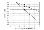
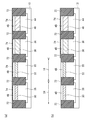
図1及び図2は、本実施形態による半導体装置の構造を示す概略断面図である。図3乃至図21は、本実施形態による半導体装置の製造方法を示す工程断面図である。図22は、低電圧トランジスタの閾値電圧とエピタキシャルシリコン層の堆積膜厚との関係を示すグラフである。 1 and 2 are schematic cross-sectional views illustrating the structure of the semiconductor device according to the present embodiment. 3 to 21 are process cross-sectional views illustrating the method for fabricating the semiconductor device according to the present embodiment. FIG. 22 is a graph showing the relationship between the threshold voltage of the low voltage transistor and the deposited film thickness of the epitaxial silicon layer.
はじめに、本実施形態による半導体装置の構造について図1及び図2を用いて説明する。 First, the structure of the semiconductor device according to the present embodiment will be explained with reference to FIGS.
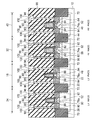
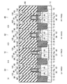
シリコン基板10上には、低電圧NMOSトランジスタ形成領域24、低電圧PMOSトランジスタ形成領域16、高電圧NMOSトランジスタ形成領域32、高電圧PMOSトランジスタ形成領域40が設けられている。各トランジスタ形成領域には、素子分離絶縁膜72によって活性領域が画定されている。
On the
低電圧PMOSトランジスタ形成領域16のシリコン基板10内には、Nウェル20と、N型高濃度不純物層22とが形成されている。N型高濃度不純物層22上には、シリコン基板10上にエピタキシャル成長されたシリコン層48が形成されている。シリコン層48上には、ゲート絶縁膜78aが形成されている。ゲート絶縁膜78a上には、ゲート電極80が形成されている。ゲート電極80の両側のシリコン層48及びシリコン基板10内には、ソース/ドレイン領域94が形成されている。これらにより、低電圧PMOSトランジスタ(LV PMOS)が形成されている。
An N well 20 and an N type high
低電圧NMOSトランジスタ形成領域24のシリコン基板10内には、Pウェル28と、P型高濃度不純物層30とが形成されている。P型高濃度不純物層30上には、シリコン基板10上にエピタキシャル成長され、シリコン層48よりも薄いシリコン層52が形成されている。シリコン層52上には、ゲート絶縁膜78aが形成されている。ゲート絶縁膜78a上には、ゲート電極80が形成されている。ゲート電極80の両側のシリコン層52及びシリコン基板10内には、ソース/ドレイン領域92が形成されている。これらにより、低電圧NMOSトランジスタ(LV NMOS)が形成されている。
A P well 28 and a P type high
低電圧PMOSトランジスタ及び低電圧NMOSトランジスタは、主に、高速動作が必要とされる回路部分に用いられるものである。 The low-voltage PMOS transistor and the low-voltage NMOS transistor are mainly used for circuit portions that require high-speed operation.
高電圧NMOSトランジスタ形成領域32のシリコン基板10内には、Pウェル36と、P型不純物層38とが形成されている。P型不純物層38は、接合耐圧やホットキャリア耐性を向上するために、低電圧NMOSトランジスタのP型高濃度不純物層30よりも低濃度且つなだらかな不純物分布になっている。P型不純物層38上には、シリコン基板10上にエピタキシャル成長されたシリコン層52が形成されている。シリコン層52上には、低電圧トランジスタのゲート絶縁膜78aよりも厚いゲート絶縁膜74aが形成されている。ゲート絶縁膜74a上には、ゲート電極80が形成されている。ゲート電極80の両側のシリコン層52及びシリコン基板10内には、ソース/ドレイン領域92が形成されている。これらにより、高電圧NMOSトランジスタ(HV NMOS)が形成されている。
A P well 36 and a P
高電圧PMOSトランジスタ形成領域40のシリコン基板10内には、Nウェル44と、N型不純物層46とが形成されている。N型不純物層46は、接合耐圧やホットキャリア耐性を向上するために、低電圧PMOSトランジスタのN型高濃度不純物層22よりも低濃度且つなだらかな不純物分布になっている。N型不純物層46上には、シリコン基板10上にエピタキシャル成長されたシリコン層52が形成されている。シリコン層52上には、低電圧トランジスタのゲート絶縁膜78aよりも厚いゲート絶縁膜74aが形成されている。ゲート絶縁膜74a上には、ゲート電極80が形成されている。ゲート電極80の両側のシリコン層52及びシリコン基板10内には、ソース/ドレイン領域94が形成されている。これらにより、高電圧PMOSトランジスタ(HV PMOS)が形成されている。
An N well 44 and an N
高電圧NMOSトランジスタ及び高電圧PMOSトランジスタは、3.3V I/O等、高電圧の印加される回路部分に用いられるものである。 The high voltage NMOS transistor and the high voltage PMOS transistor are used for a circuit portion to which a high voltage is applied, such as 3.3 V I / O.
各トランジスタのゲート電極80上及びソース/ドレイン領域92,94上には、金属シリサイド膜96が形成されている。
A
4種類のトランジスタが形成されたシリコン基板10上には、層間絶縁膜98が形成されている。層間絶縁膜98には、トランジスタに接続されたコンタクトプラグ100が埋め込まれている。コンタクトプラグ100には、配線102が接続されている。
An interlayer insulating
このように、本実施形態による半導体装置は、低電圧PMOSトランジスタ及び低電圧NMOSトランジスタの2種類の低電圧トランジスタと、高電圧NMOSトランジスタ及び高電圧PMOSトランジスタの2種類の高電圧トランジスタとを有している。 As described above, the semiconductor device according to the present embodiment includes two types of low voltage transistors, a low voltage PMOS transistor and a low voltage NMOS transistor, and two types of high voltage transistors, a high voltage NMOS transistor and a high voltage PMOS transistor. ing.
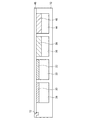
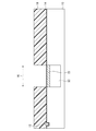
低電圧トランジスタは、例えば図2に示すように、チャネル領域206に、急峻な不純物濃度分布を有する高濃度不純物層208と、高濃度不純物層208上にエピタキシャル成長されたノンドープのシリコン層210とを有するものである。図2の高濃度不純物層208及びシリコン層210は、低電圧PMOSトランジスタのN型高濃度不純物層22及びシリコン層48に、低電圧NMOSトランジスタのP型高濃度不純物層30及びシリコン層52に、それぞれ相当する。高濃度不純物層上にノンドープのエピタキシャル層を有するトランジスタ構造は、不純物の統計的揺らぎによるトランジスタの閾値電圧ばらつきを抑制するために有効である。
For example, as illustrated in FIG. 2, the low-voltage transistor includes a high-
ただし、NMOSトランジスタとPMOSトランジスタとでは、高濃度不純物層208を形成する不純物が異なっており、これら不純物の拡散速度も異なっている。例えば、後述する参考例の場合では、PMOSトランジスタの高濃度不純物層を形成する砒素のシリコン層210中への拡散が、NMOSトランジスタの高濃度不純物層208を形成するボロンのシリコン層210中への拡散よりも速くなる。すなわち、PMOSトランジスタでは、NMOSトランジスタと比較して、高濃度不純物層208がよりシリコン層210側に分布する(図46参照)。
However, the impurities forming the high-
高濃度不純物層208上にノンドープのシリコン層210を有するトランジスタの閾値電圧は、高濃度不純物層208の不純物濃度と、シリコン層210のノンドープ領域の膜厚(ゲート絶縁膜212と高濃度不純物層208との距離)とに依存する。このため、NMOSトランジスタとPMOSトランジスタとで不純物の拡散速度が異なることにより、狙い閾値電圧を得るための最適なシリコン層210の膜厚が異なることがある。その結果、後述する参考例のようにNMOSトランジスタとPMOSトランジスタとでエピタキシャルシリコン層の膜厚を同じにした場合、NMOSトランジスタ及びPMOSトランジスタの双方に最適な不純物プロファイルを実現することが困難である。
The threshold voltage of the transistor having the
これに対し、本実施形態による半導体装置では、N型不純物とP型不純物との拡散速度の違いを考慮して、PMOSトランジスタ形成領域に形成するシリコン層48の膜厚と、NMOSトランジスタ形成領域に形成するシリコン層52の膜厚とを変えている。具体的には、N型高濃度不純物層22を形成する不純物のエピタキシャル層方向への拡散よりも速い場合、例えば、N型高濃度不純物層22を形成する不純物をAsとし、P型高濃度不純物層30を形成する不純物をB/Cとした場合を考慮して、シリコン層52の膜厚よりもシリコン層48の膜厚を厚くしている。これにより、NMOSトランジスタ及びPMOSトランジスタの双方において、エピタキシャルシリコン層の膜厚を、狙い閾値電圧を得るための最適な膜厚にすることができる。
On the other hand, in the semiconductor device according to the present embodiment, considering the difference in diffusion rate between the N-type impurity and the P-type impurity, the thickness of the
なお、P型高濃度不純物層30を形成する不純物のエピタキシャル層方向への拡散がN型高濃度不純物層22を形成する不純物のエピタキシャル層方向への拡散よりも速い場合、例えば、P型高濃度不純物層30を形成する不純物をB/Cとし、N型高濃度不純物層22を形成する不純物をSbとした場合には、NMOSとPMOSとでシリコン層の膜厚の関係を逆にしてもよい。また、本実施形態では、高電圧トランジスタ形成領域のシリコン層52の膜厚を、低電圧NMOSトランジスタのシリコン層52の膜厚と同じにしているが、低電圧PMOSトランジスタのシリコン層48の膜厚と同じにしてもよい。高電圧トランジスタ形成領域のシリコン層52の膜厚は、低電圧NMOSトランジスタのシリコン層52の膜厚及び低電圧PMOSトランジスタのシリコン層48の膜厚と異なってもよい。
In the case where diffusion of impurities forming the P-type high
各トランジスタ領域に形成するエピタキシャルシリコン層の膜厚は、各トランジスタに求められる特性に応じて、適宜変更することができる。 The film thickness of the epitaxial silicon layer formed in each transistor region can be appropriately changed according to the characteristics required for each transistor.
次に、本実施形態による半導体装置の製造方法について図3乃至図21を用いて説明する。 Next, the method for fabricating the semiconductor device according to the present embodiment will be explained with reference to FIGS.
まず、フォトリソグラフィ及びエッチングにより、シリコン基板10の製品形成領域外(例えば、スクライブ領域)に、マスクアライメント用のマークとして用いる溝12を形成する。
First, a
本実施形態による半導体装置の製造方法では、素子分離絶縁膜72の形成前に、ウェルやチャネル不純物層を形成する。溝12は、素子分離絶縁膜72の形成前に行われるリソグラフィー工程(ウェルやチャネル不純物層の形成等)において、マスクアライメント用のマークとして用いられるものである。
In the method for manufacturing the semiconductor device according to the present embodiment, a well and a channel impurity layer are formed before the element
次いで、シリコン基板10の全面に、例えば熱酸化法により、シリコン基板10の表面の保護膜としてのシリコン酸化膜14を形成する(図3)。
Next, a
次いで、フォトリソグラフィにより、低電圧PMOSトランジスタ形成領域16を露出し、他の領域を覆うフォトレジスト膜18を形成する。フォトリソグラフィの位置合わせには、溝12のマークを用いる。
Next, a
次いで、フォトレジスト膜18をマスクとしてイオン注入を行い、シリコン基板10の低電圧PMOSトランジスタ形成領域16に、Nウェル20と、N型高濃度不純物層22とを形成する(図4)。
Next, ion implantation is performed using the
Nウェル20は、例えば、リンイオン(P+)を、加速エネルギー360keV、ドーズ量7.5×1012cm−2の条件で、基板法線方向に対して傾斜した4方向からそれぞれイオン注入することにより形成する。N型高濃度不純物層22は、例えば、砒素イオン(As+)を、加速エネルギー6keV、ドーズ量2×1013cm−2の条件でイオン注入することにより形成する。砒素イオンに代えて、アンチモンイオン(Sb+)を、加速エネルギー20keV、ドーズ量1×1013cm−2の条件でイオン注入することにより形成してもよい。
In the N well 20, for example, phosphorus ions (P + ) are ion-implanted from four directions inclined with respect to the substrate normal direction under the conditions of an acceleration energy of 360 keV and a dose of 7.5 × 10 12 cm −2. To form. The N-type high
次いで、例えばアッシングにより、フォトレジスト膜18を除去する。
Next, the
次いで、フォトリソグラフィにより、低電圧NMOSトランジスタ形成領域24を露出し、他の領域を覆うフォトレジスト膜26を形成する。フォトリソグラフィの位置合わせには、溝12のマークを用いる。
Next, a
次いで、フォトレジスト膜26をマスクとしてイオン注入を行い、シリコン基板10の低電圧NMOSトランジスタ形成領域24に、Pウェル28と、P型高濃度不純物層30とを形成する(図5)。
Next, ion implantation is performed using the
Pウェル28は、例えば、ボロンイオン(B+)を、加速エネルギー150keV、ドーズ量7.5×1012cm−2の条件で、基板法線方向に対して傾斜した4方向から、それぞれイオン注入することにより形成する。P型高濃度不純物層30は、例えば、ゲルマニウムイオン(Ge+)を、加速エネルギー50keV、ドーズ量5×1014cm−2の条件で、炭素イオン(C+)を、加速エネルギー3keV、ドーズ量3×1014cm−2の条件で、ボロンイオンを、加速エネルギー2keV、ドーズ量3×1013cm−2の条件で、それぞれイオン注入することにより形成する。ゲルマニウムは、シリコン基板10を非晶質化してボロンイオンのチャネリングを防止するとともに、シリコン基板10を非晶質化して炭素が格子点に配される確率を高めるように作用する。格子点に配された炭素は、ボロンの拡散を抑制するように作用する。かかる観点から、ゲルマニウムは、炭素及びボロンよりも先にイオン注入する。Pウェル20は、P型高濃度不純物層30よりも先に形成することが望ましい。
In the P well 28, for example, boron ions (B + ) are ion-implanted from four directions inclined with respect to the substrate normal direction under the conditions of an acceleration energy of 150 keV and a dose of 7.5 × 10 12 cm −2. To form. The P-type high-
次いで、例えばアッシングにより、フォトレジスト膜26を除去する。
Next, the
次いで、フォトリソグラフィにより、高電圧NMOSトランジスタ形成領域32を露出し、他の領域を覆うフォトレジスト膜34を形成する。フォトリソグラフィの位置合わせには、溝12のマークを用いる。
Next, a
次いで、フォトレジスト膜34をマスクとしてイオン注入を行い、シリコン基板10の高電圧NMOSトランジスタ形成領域32に、Pウェル36と、P型不純物層38とを形成する(図6)。
Next, ion implantation is performed using the
Pウェル36は、例えば、ボロンイオンを、加速エネルギー150keV、ドーズ量7.5×1012cm−2の条件で、基板法線方向に対して傾斜した4方向から、それぞれイオン注入することにより形成する。P型不純物層38は、例えば、ボロンイオンを、加速エネルギー2keV、ドーズ量5×1012cm−2の条件でイオン注入することにより形成する。なお、高電圧動作のNMOSトランジスタでは、チャネル領域の不純物濃度分布をなだらかにして接合耐圧、ホットキャリア耐性を改善する観点から、炭素及びゲルマニウムのイオン注入を行っていない。
The P well 36 is formed, for example, by implanting boron ions from four directions inclined with respect to the normal direction of the substrate under conditions of an acceleration energy of 150 keV and a dose of 7.5 × 10 12 cm −2. To do. The P-
次いで、例えばアッシングにより、フォトレジスト膜34を除去する。
Next, the
次いで、フォトリソグラフィにより、高電圧PMOSトランジスタ形成領域40を露出し、他の領域を覆うフォトレジスト膜42を形成する。フォトリソグラフィの位置合わせには、溝12のマークを用いる。
Next, a
次いで、フォトレジスト膜42をマスクとしてイオン注入を行い、シリコン基板10の高電圧PMOSトランジスタ形成領域40に、Nウェル44と、N型不純物層46とを形成する(図7)。
Next, ion implantation is performed using the
Nウェル44は、例えば、リンイオンを、加速エネルギー360keV、ドーズ量7.5×1012cm−2の条件で、基板法線方向に対して傾斜した4方向から、それぞれイオン注入することにより形成する。N型不純物層46は、例えば、リンイオンを、加速エネルギー2keV、ドーズ量5×1012cm−2の条件でイオン注入することにより形成する。なお、高電圧動作のNMOSトランジスタでは、チャネル領域の不純物濃度分布をなだらかにして接合耐圧、ホットキャリア耐性を改善する観点から、砒素又はアンチモンに代えてリンのイオン注入を行っている。
The N well 44 is formed, for example, by implanting phosphorous ions from four directions inclined with respect to the substrate normal direction under the conditions of an acceleration energy of 360 keV and a dose of 7.5 × 10 12 cm −2. . The N-
次いで、例えばアッシングにより、フォトレジスト膜42を除去する。
Next, the
なお、各トランジスタ形成領域に行うイオン注入は、どの領域から行ってもよい。 Note that ion implantation performed in each transistor formation region may be performed from any region.
次いで、不活性雰囲気中で熱処理を行い、シリコン基板10に導入されたイオン注入ダメージを回復するとともに、注入した不純物を活性化する。例えば、窒素雰囲気中で、600℃150秒の熱処理を行い、次いで、1000℃0秒の熱処理を行う。
Next, heat treatment is performed in an inert atmosphere to recover the ion implantation damage introduced into the
この際、P型高濃度不純物層30にはボロンとともにゲルマニウム及び炭素を導入しているため、ボロンのみを導入しているP型不純物層38と比較して、ボロンの拡散を抑制することができる。これにより、P型高濃度不純物層30の急峻な分布を維持しつつ、P型不純物層38の不純物をブロードに分布させることができる。
At this time, since germanium and carbon are introduced into the P-type high
また、N型高濃度不純物層22は、N型不純物層46を形成する燐よりも拡散定数の小さい砒素を用いて形成されているため、N型高濃度不純物層22の急峻な分布を維持しつつ、N型不純物層46の不純物をブロードに分布させることができる。
Further, since the N-type high
次いで、例えば弗酸水溶液を用いたウェットエッチングにより、シリコン酸化膜14を除去する。
Next, the
次いで、例えばCVD法により、シリコン基板10の表面に、例えば膜厚34nmのノンドープのシリコン層48をエピタキシャル成長する(図8)。
Next, a
次いで、フォトリソグラフィにより、低電圧NMOSトランジスタ形成領域24及び高電圧トランジスタ形成領域32,40を露出し、他の領域を覆うフォトレジスト膜50を形成する。フォトリソグラフィの位置合わせには、溝12のマークを用いる。なお、砒素に代えてアンチモンを用いた場合は、低電圧PMOSトランジスタ形成領域16及び高電圧トランジスタ形成領域32,40を露出し、他の領域を覆うフォトレジスト膜50を形成する。以下の工程では、砒素を用いた場合を想定して説明する。
Next, a
次いで、フォトレジスト膜50をマスクとして、例えばTMAHやフッ硝酸水溶液(HF/HNO3/H2O)を用いたウェットエッチングを行い、フォトレジスト膜50で覆われていない領域のシリコン層48を、8nm程度エッチングする(図9)。
Next, using the
次いで、例えばアッシングにより、フォトレジスト膜50を除去する。
Next, the
こうして、低電圧PMOSトランジスタ形成領域16に膜厚34nmのシリコン層48を形成し、低電圧NMOSトランジスタ形成領域24及び高電圧トランジスタ形成領域32,40に膜厚26nmのシリコン層52を形成する(図10)。
Thus, a
前述のように、N型高濃度不純物層22を形成する砒素のシリコン層48方向への拡散は、P型高濃度不純物層30を形成するボロンのシリコン層52方向への拡散よりも10nm程度大きい。このため、狙い閾値電圧を得るための最適なシリコン層の堆積膜厚も、低電圧PMOSトランジスタと低電圧NMOSトランジスタとで異なってくる。
As described above, the diffusion of arsenic in the direction of the
図22は、低電圧トランジスタの閾値電圧とエピタキシャルシリコン層の堆積膜厚との関係の一例を示すグラフである。縦軸は、閾値電圧の絶対値を表し、横軸はシリコン層の堆積膜厚を表している。図中、■印のプロットがPMOSであり、◆印のプロットがNMOSである。 FIG. 22 is a graph showing an example of the relationship between the threshold voltage of the low voltage transistor and the deposited film thickness of the epitaxial silicon layer. The vertical axis represents the absolute value of the threshold voltage, and the horizontal axis represents the deposited film thickness of the silicon layer. In the figure, the ■ mark plot is PMOS, and the ◆ mark plot is NMOS.
図22に示すように、閾値電圧の絶対値は、シリコン層の堆積膜厚が増加するほどに低くなる傾向にある。ここで、例えば、低電圧NMOSトランジスタの狙い閾値電圧を0.30Vと仮定すると、低電圧NMOSトランジスタに最適なシリコン層の堆積膜厚は、26nm程度となる。一方、低電圧PMOSトランジスタの狙い閾値電圧を−0.33Vと仮定すると(図中、一点鎖線)、低電圧PMOSトランジスタに最適なシリコン層の堆積膜厚は、34nm程度となる。 As shown in FIG. 22, the absolute value of the threshold voltage tends to decrease as the deposited film thickness of the silicon layer increases. Here, for example, if the target threshold voltage of the low voltage NMOS transistor is assumed to be 0.30 V, the optimum deposited film thickness of the silicon layer for the low voltage NMOS transistor is about 26 nm. On the other hand, assuming that the target threshold voltage of the low-voltage PMOS transistor is −0.33 V (indicated by a one-dot chain line in the figure), the optimum deposited film thickness of the silicon layer for the low-voltage PMOS transistor is about 34 nm.
したがって、図22に示す例の場合、シリコン層48の膜厚を34nm程度に設定し、シリコン層52の膜厚を26nm程度に設定することにより、低電圧NMOSトランジスタ及び低電圧PMOSトランジスタの双方において、狙い閾値電圧を得ることができる。
Therefore, in the case of the example shown in FIG. 22, by setting the film thickness of the
シリコン層48,52の膜厚の作り分けは、1つのリソグラフィー工程と1つのエッチング工程を追加するだけの簡単なプロセスにより行うことができ、製造コストの大幅な増加をもたらすこともない。 The film thicknesses of the silicon layers 48 and 52 can be separately formed by a simple process in which one lithography process and one etching process are added, and the manufacturing cost is not significantly increased.
シリコン層48及びシリコン層52の膜厚は、N型高濃度不純物層22を形成する不純物の拡散速度、P型高濃度不純物層30を形成する不純物の拡散速度、狙い閾値電圧を得るための最適なノンドープ領域の膜厚等に応じて、適宜設定することが望ましい。
The film thicknesses of the
次いで、例えばISSG(in-situ steam generation)法により、減圧下でシリコン層48の表面をウェット酸化し、例えば膜厚3nmのシリコン酸化膜66を形成する。処理条件は、例えば、温度を810℃、時間を20秒間とする。
Next, the surface of the
次いで、シリコン酸化膜66上に、例えばLPCVD法により、例えば膜厚90nmのシリコン窒化膜68を堆積する。処理条件は、例えば、温度を700℃、時間を150分間とする。
Next, a
次いで、フォトリソグラフィ及びドライエッチングにより、シリコン窒化膜68、シリコン酸化膜66、シリコン層48,52、及びシリコン基板10を異方性エッチングし、各トランジスタ形成領域の間の領域を含む素子分離領域に、素子分離溝70を形成する(図11)。なお、フォトリソグラフィの位置合わせには、溝12のマークを用いる。
Next, the
次いで、例えばISSG法により、減圧下でシリコン層48,52及びシリコン基板10の表面をウェット酸化し、素子分離溝70の内壁に、ライナー膜として、例えば膜厚2nmのシリコン酸化膜を形成する。処理条件は、例えば、温度を810℃、時間を12秒間とする。
Next, the silicon layers 48 and 52 and the surface of the
次いで、例えば高密度プラズマCVD法により、例えば膜厚500nmのシリコン酸化膜を堆積し、素子分離溝70をシリコン酸化膜によって埋め込む。
Next, a silicon oxide film having a thickness of, for example, 500 nm is deposited by, for example, a high-density plasma CVD method, and the
次いで、例えばCMP法により、シリコン窒化膜68上のシリコン酸化膜を除去する。こうして、いわゆるSTI(Shallow Trench Isolation)法により、素子分離溝70に埋め込まれたシリコン酸化膜により、素子分離絶縁膜72を形成する(図12)。
Next, the silicon oxide film on the
次いで、シリコン窒化膜68をマスクとして、例えば弗酸水溶液を用いたウェットエッチングにより、素子分離絶縁膜72を、例えば30nm程度エッチングする。このエッチングは、完成したトランジスタにおいて、シリコン層48,52の表面の高さと素子分離絶縁膜72の表面の高さとが同程度になるように調整するためのものである。
Next, using the
次いで、例えばホットリン酸を用いたウェットエッチングにより、シリコン窒化膜68を除去する(図13)。
Next, the
次いで、例えば弗酸水溶液を用いたウェットエッチングにより、シリコン酸化膜66を除去する。
Next, the
次いで、熱酸化法により、例えば膜厚7nmのシリコン酸化膜74を形成する(図14)。処理条件は、例えば、温度を750℃、時間を52分間とする。
Next, a
次いで、フォトリソグラフィにより、高電圧トランジスタ形成領域32,40を覆い、低電圧トランジスタ形成領域16,24を露出するフォトレジスト膜76を形成する。
Next, a
次いで、例えば弗酸水溶液を用いたウェットエッチングにより、フォトレジスト膜76をマスクとしてシリコン酸化膜74をエッチングする。これにより、低電圧PMOSトランジスタ形成領域16及び低電圧NMOSトランジスタ形成領域24のシリコン酸化膜74を除去する(図15)。
Next, the
次いで、例えばアッシングにより、フォトレジスト膜76を除去する。
Next, the
次いで、熱酸化法により、例えば膜厚2nmのシリコン酸化膜78を形成する。処理条件は、例えば、温度を810℃、時間を8秒間とする。
Next, a
次いで、NO雰囲気中で、例えば870℃、13秒間の熱処理を行い、シリコン酸化膜74,78内に窒素を導入する。
Next, in a NO atmosphere, for example, heat treatment is performed at 870 ° C. for 13 seconds to introduce nitrogen into the
こうして、高電圧NMOSトランジスタ形成領域32及び高電圧PMOSトランジスタ形成領域40に、シリコン酸化膜74のゲート絶縁膜74aを形成する。また、低電圧PMOSトランジスタ形成領域16及び低電圧NMOSトランジスタ形成領域24に、シリコン酸化膜74よりも薄いシリコン酸化膜78のゲート絶縁膜78aを形成する(図16)。
Thus, the
次いで、全面に、例えばLPCVD法により、例えば膜厚100nmのノンドープのポリシリコン膜を堆積する。処理条件は、例えば、温度を605℃とする。 Next, a non-doped polysilicon film of, eg, a 100 nm-thickness is deposited on the entire surface by, eg, LPCVD. The processing conditions are, for example, a temperature of 605 ° C.
次いで、フォトリソグラフィ及びドライエッチングにより、ポリシリコン膜をパターニングし、各トランジスタ形成領域にゲート電極80を形成する(図17)。
Next, the polysilicon film is patterned by photolithography and dry etching, and a
次いで、フォトリソグラフィ及びイオン注入により、高電圧NMOSトランジスタ形成領域32に、ゲート電極80をマスクとしてN型不純物を選択的にイオン注入し、LDD領域となるN型不純物層82を形成する。例えば、リンイオンを、加速エネルギー35keV、ドーズ量2×1013cm−2の条件でイオン注入し、N型不純物層82を形成する。
Next, by photolithography and ion implantation, N-type impurities are selectively ion-implanted into the high-voltage NMOS
次いで、フォトリソグラフィ及びイオン注入により、高電圧PMOSトランジスタ形成領域40に、ゲート電極80をマスクとしてP型不純物を選択的にイオン注入し、LDD領域となるP型不純物層84を形成する。例えば、ボロンイオンを、加速エネルギー10keV、ドーズ量2×1013cm−2の条件でイオン注入し、P型不純物層84を形成する。
Next, by photolithography and ion implantation, P-type impurities are selectively ion-implanted into the high-voltage PMOS
次いで、フォトリソグラフィ及びイオン注入により、低電圧NMOSトランジスタ形成領域24に、ゲート電極80をマスクとしてN型不純物を選択的にイオン注入し、エクステンション領域となるN型不純物層86を形成する。例えば、砒素イオンを、加速エネルギー6keV、ドーズ量2×1014cm−2の条件でイオン注入し、N型不純物層86を形成する。
Next, by photolithography and ion implantation, N-type impurities are selectively ion-implanted into the low-voltage NMOS
次いで、フォトリソグラフィ及びイオン注入により、低電圧PMOSトランジスタ形成領域16に、ゲート電極66をマスクとして選択的にイオン注入し、エクステンション領域となるP型不純物層88を形成する(図18)。例えば、ボロンイオンを、加速エネルギー0.6keV、ドーズ量7×1014cm−2の条件でイオン注入し、P型不純物層88を形成する。
Next, by photolithography and ion implantation, ions are selectively implanted into the low-voltage PMOS
次いで、全面に、例えばCVD法により、例えば膜厚80nmのシリコン酸化膜を堆積する。処理条件は、例えば、温度を520℃とする。 Next, a silicon oxide film of, eg, a 80 nm-thickness is deposited on the entire surface by, eg, CVD. The processing conditions are, for example, a temperature of 520 ° C.
次いで、全面に堆積したシリコン酸化膜を異方性エッチングし、ゲート電極80の側壁部分に選択的に残存させる。これにより、シリコン酸化膜のサイドウォールスペーサ90を形成する(図19)。
Next, the silicon oxide film deposited on the entire surface is anisotropically etched to selectively remain on the side wall portion of the
次いで、フォトリソグラフィ及びイオン注入により、低電圧NMOSトランジスタ形成領域24及び高電圧NMOSトランジスタ形成領域32に、ゲート電極80及びサイドウォールスペーサ90をマスクとして選択的にイオン注入する。これにより、ソース/ドレイン領域となるN型不純物層92を形成するとともに、NMOSトランジスタのゲート電極80にN型不純物を添加する。イオン注入条件は、例えば、リンイオンを、加速エネルギー8keV、ドーズ量1.2×1016cm−2とする。
Next, ions are selectively implanted into the low-voltage NMOS
次いで、フォトリソグラフィ及びイオン注入により、低電圧PMOSトランジスタ形成領域16及び高電圧PMOSトランジスタ形成領域40に、ゲート電極80及びサイドウォールスペーサ90をマスクとして選択的にイオン注入する。これにより、ソース/ドレイン領域となるP型不純物層94を形成するとともに、PMOSトランジスタのゲート電極80にP型不純物を添加する。イオン注入条件は、例えば、ボロンイオンを、加速エネルギー4keV、ドーズ量6×1015cm−2とする。
Next, ions are selectively implanted into the low-voltage PMOS
次いで、不活性ガス雰囲気中で、例えば1025℃、0秒間の短時間熱処理を行い、注入した不純物の活性化及びゲート電極80中の拡散を行う。1025℃、0秒間の短時間熱処理は、ゲート電極80とゲート絶縁膜との界面まで不純物を拡散させるのに十分である。
Next, a short-time heat treatment is performed in an inert gas atmosphere at, for example, 1025 ° C. for 0 second to activate the implanted impurities and diffuse the
こうして、シリコン基板10上に、4種類のトランジスタを完成する。すなわち、低電圧NMOSトランジスタ形成領域24に、低電圧NMOSトランジスタ(LV NMOS)を形成する。また、低電圧PMOSトランジスタ形成領域16に、低電圧PMOSトランジスタ(LV PMOS)を形成する。また、高電圧NMOSトランジスタ形成領域32に、高電圧NMOSトランジスタ(HV NMOS)を形成する。また、高電圧PMOSトランジスタ形成領域に、高電圧PMOSトランジスタ(HV PMOS)を形成する(図20)。
Thus, four types of transistors are completed on the
次いで、サリサイドプロセスにより、ゲート電極80上、N型不純物層92上、及びP型不純物層94上に、金属シリサイド膜96、例えばコバルトシリサイド膜を形成する。
Next, a
次いで、全面に、例えばCVD法により、例えば膜厚50nmのシリコン窒化膜を堆積し、エッチングストッパ膜としてのシリコン窒化膜を形成する。 Next, a silicon nitride film of, eg, a 50 nm-thickness is deposited on the entire surface by, eg, CVD, to form a silicon nitride film as an etching stopper film.
次いで、シリコン窒化膜上に、例えば高密度プラズマCVD法により、例えば膜厚500nmのシリコン酸化膜を堆積する。 Next, a silicon oxide film of, eg, a 500 nm-thickness is deposited on the silicon nitride film by, eg, high density plasma CVD.
これにより、シリコン窒化膜とシリコン酸化膜との積層膜の層間絶縁膜98を形成する。
Thereby, an
次いで、例えばCMP法により、層間絶縁膜98の表面を研磨し、平坦化する。
Next, the surface of the
この後、層間絶縁膜98に埋め込まれたコンタクトプラグ100、コンタクトプラグ100に接続された配線102等を形成し、半導体装置を完成する(図21)。
Thereafter, the
このように、本実施形態によれば、N型不純物とP型不純物との拡散速度の違いを考慮して、低電圧PMOSトランジスタ形成領域と低電圧NMOSトランジスタ形成領域とで、エピタキシャルシリコン層の膜厚を変化している。これにより、NMOSトランジスタ及びPMOSトランジスタの双方において、エピタキシャルシリコン層を狙い閾値電圧を得るための最適な膜厚にすることができ、閾値電圧の制御性を向上することができる。これにより、半導体装置の信頼性を高めることができる。 Thus, according to the present embodiment, in consideration of the difference in diffusion rate between the N-type impurity and the P-type impurity, the epitaxial silicon layer film is formed between the low-voltage PMOS transistor formation region and the low-voltage NMOS transistor formation region. The thickness is changing. Thereby, in both the NMOS transistor and the PMOS transistor, the epitaxial silicon layer can be aimed at an optimum film thickness for obtaining the threshold voltage, and the controllability of the threshold voltage can be improved. Thereby, the reliability of the semiconductor device can be improved.
[第2実施形態]
第2実施形態による半導体装置の製造方法について図23乃至図28を用いて説明する。図1乃至図22に示す第1実施形態による半導体装置及びその製造方法と同一の構成要素には同一の符号を付し説明を省略し又は簡潔にする。
[Second Embodiment]
A method for fabricating a semiconductor device according to the second embodiment will be described with reference to FIGS. The same components as those of the semiconductor device and the manufacturing method thereof according to the first embodiment shown in FIGS. 1 to 22 are denoted by the same reference numerals, and description thereof will be omitted or simplified.
図23乃至図28は、本実施形態による半導体装置の製造方法を示す工程断面図である。 23 to 28 are process cross-sectional views illustrating the method for fabricating the semiconductor device according to the present embodiment.
本実施形態では、図1に示す第1実施形態による半導体装置の他の製造方法を説明する。 In the present embodiment, another method for manufacturing the semiconductor device according to the first embodiment shown in FIG. 1 will be described.
まず、図3乃至図7に示す第1実施形態による半導体装置の製造方法と同様にして、シリコン基板10内に、Nウェル20,44、Pウェル28,36、N型高濃度不純物層22、P型高濃度不純物層30、P型不純物層38、N型不純物層46等を形成する(図7参照)。
First, in the same manner as the semiconductor device manufacturing method according to the first embodiment shown in FIGS. 3 to 7,
次いで、例えばアッシングにより、フォトレジスト膜42を除去する。
Next, the
次いで、不活性雰囲気中で熱処理を行い、シリコン基板10に導入されたイオン注入ダメージを回復するとともに、注入した不純物を活性化する。
Next, heat treatment is performed in an inert atmosphere to recover the ion implantation damage introduced into the
次いで、例えば弗酸水溶液を用いたウェットエッチングにより、シリコン酸化膜14を除去する。
Next, the
次いで、例えばCVD法により、シリコン基板10の表面に、例えば膜厚26nmのノンドープのシリコン層54をエピタキシャル成長する(図23)。
Next, a
次いで、例えばCVD法により、シリコン層54上に、例えば膜厚3nmのシリコン酸化膜56を形成する。
Next, a
次いで、シリコン酸化膜56上に、フォトリソグラフィにより、低電圧PMOSトランジスタ形成領域16を露出し、他の領域を覆うフォトレジスト膜58を形成する(図24)。フォトリソグラフィの位置合わせには、溝12のマークを用いる。
Next, a
次いで、フォトレジスト膜58をマスクとして、例えば弗酸水溶液を用いたウェットエッチング又はドライエッチングにより、低電圧PMOSトランジスタ形成領域16のシリコン酸化膜58を除去する(図25)。
Next, using the
次いで、例えばアッシングにより、フォトレジスト膜58を除去する(図26)。
Next, the
次いで、パターニングしたシリコン酸化膜56をマスクとして、シリコン酸化膜56により覆われていない領域のシリコン層54上に、例えば膜厚8nmのノンドープのシリコン層60を選択的にエピタキシャル成長する(図27)。
Next, a
次いで、例えば弗酸水溶液を用いたウェットエッチング又はドライエッチングにより、シリコン酸化膜58を除去する。
Next, the
こうして、低電圧PMOSトランジスタ形成領域16に、膜厚26nmのシリコン層54と膜厚10nmのシリコン層60との積層膜により、膜厚34nmのシリコン層48を形成する。また、低電圧NMOSトランジスタ形成領域24及び高電圧トランジスタ形成領域32,40に、膜厚20nmのシリコン層54により、シリコン層52を形成する。
Thus, a
この後、図11乃至図21に示す第1実施形態による半導体装置の製造方法と同様にして、図1に示す第1実施形態による半導体装置を完成する。 Thereafter, the semiconductor device according to the first embodiment shown in FIG. 1 is completed in the same manner as the semiconductor device manufacturing method according to the first embodiment shown in FIGS.
このように、本実施形態によれば、N型不純物とP型不純物との拡散速度の違いを考慮して、低電圧PMOSトランジスタ形成領域と低電圧NMOSトランジスタ形成領域とで、エピタキシャルシリコン層の膜厚を変化している。これにより、NMOSトランジスタ及びPMOSトランジスタの双方において、エピタキシャルシリコン層を狙い閾値電圧を得るための最適な膜厚にすることができ、閾値電圧の制御性を向上することができる。これにより、半導体装置の信頼性を高めることができる。 Thus, according to the present embodiment, in consideration of the difference in diffusion rate between the N-type impurity and the P-type impurity, the epitaxial silicon layer film is formed between the low-voltage PMOS transistor formation region and the low-voltage NMOS transistor formation region. The thickness is changing. Thereby, in both the NMOS transistor and the PMOS transistor, the epitaxial silicon layer can be aimed at an optimum film thickness for obtaining the threshold voltage, and the controllability of the threshold voltage can be improved. Thereby, the reliability of the semiconductor device can be improved.
[第3実施形態]
第3実施形態による半導体装置の製造方法について図29乃至図39を用いて説明する。図1乃至図28に示す第1及び第2実施形態による半導体装置及びその製造方法と同一の構成要素には同一の符号を付し説明を省略し又は簡潔にする。
[Third Embodiment]
A method for fabricating a semiconductor device according to the third embodiment will be described with reference to FIGS. The same components as those of the semiconductor device and the manufacturing method thereof according to the first and second embodiments shown in FIG. 1 to FIG.
図29は、本実施形態による半導体装置の構造を示す概略断面図である。図30乃至図39は、本実施形態による半導体装置の製造方法を示す工程断面図である。 FIG. 29 is a schematic cross-sectional view showing the structure of the semiconductor device according to the present embodiment. 30 to 39 are process cross-sectional views illustrating the method for fabricating the semiconductor device according to the present embodiment.
はじめに、本実施形態による半導体装置の構造について図29を用いて説明する。 First, the structure of the semiconductor device according to the present embodiment will be explained with reference to FIG.
本実施形態による半導体装置は、各トランジスタの基本的な構造は、図1に示す第1実施形態による半導体装置と同様である。本実施形態による半導体装置は、低電圧PMOSトランジスタのシリコン層48の表面高さと低電圧NMOSトランジスタの表面高さとが同じである点で、第1実施形態による半導体装置とは異なっている。
In the semiconductor device according to the present embodiment, the basic structure of each transistor is the same as that of the semiconductor device according to the first embodiment shown in FIG. The semiconductor device according to the present embodiment is different from the semiconductor device according to the first embodiment in that the surface height of the
第1実施形態では、低電圧NMOSトランジスタ形成領域24のシリコン層48をエッチングしてシリコン層52を形成しているため、シリコン層48の表面高さとシリコン層52の表面高さとが異なっている。また、第2実施形態では、低電圧PMOSトランジスタ形成領域16のシリコン層54上にシリコン層60を選択成長しているため、シリコン層48の表面高さとシリコン層52の表面高さとが異なっている。
In the first embodiment, since the
シリコン層48の表面高さとシリコン層52の表面高さとを等しくすることにより、基板表面の平坦性を向上することができ、後工程の製造プロセスを容易にすることができる。また、マスクが不要であり、工程数の削減、ひいては製造コストを削減することができる。
By making the surface height of the
次に、本実施形態による半導体装置の製造方法について図30乃至図39を用いて説明する。 Next, the method for fabricating the semiconductor device according to the present embodiment will be explained with reference to FIGS.
まず、フォトリソグラフィ及びエッチングにより、シリコン基板10の製品形成領域外(例えば、スクライブ領域)に、マスクアライメント用のマークとして用いる溝12を形成する。
First, a
次いで、シリコン基板10の全面に、例えば熱酸化法により、シリコン基板10の表面の保護膜としてのシリコン酸化膜14を形成する(図30)。
Next, a
次いで、フォトリソグラフィにより、低電圧PMOSトランジスタ形成領域16を露出し、他の領域を覆うフォトレジスト膜18を形成する。フォトリソグラフィの位置合わせには、溝12のマークを用いる。
Next, a
次いで、フォトレジスト膜18をマスクとしてイオン注入を行い、シリコン基板10の低電圧PMOSトランジスタ形成領域16に、Nウェル20と、N型高濃度不純物層22とを形成する(図31)。イオン注入には、例えば第1実施形態と同じ条件を用いることができる。
Next, ion implantation is performed using the
次いで、例えばアッシングにより、フォトレジスト膜18を除去する。
Next, the
次いで、不活性雰囲気中で熱処理を行い、シリコン基板10に導入されたイオン注入ダメージを回復するとともに、注入した不純物を活性化する。例えば、窒素雰囲気中で、600℃150秒の熱処理を行う。
Next, heat treatment is performed in an inert atmosphere to recover the ion implantation damage introduced into the
次いで、例えば弗酸水溶液を用いたウェットエッチングにより、シリコン酸化膜14を除去する。
Next, the
次いで、例えばCVD法により、シリコン基板10の表面に、例えば膜厚8nmのノンドープのシリコン層60をエピタキシャル成長する(図32)。
Next, a
次いで、シリコン層60上に、例えば熱酸化法により、表面の保護膜としてのシリコン酸化膜62を形成する。
Next, a silicon oxide film 62 as a surface protective film is formed on the
次いで、フォトリソグラフィにより、高電圧NMOSトランジスタ形成領域32を露出し、他の領域を覆うフォトレジスト膜34を形成する。フォトリソグラフィの位置合わせには、溝12のマークを用いる。
Next, a
次いで、フォトレジスト膜34をマスクとしてイオン注入を行い、シリコン基板10及びシリコン層60の高電圧NMOSトランジスタ形成領域32に、Pウェル36と、P型不純物層38とを形成する(図33)。イオン注入には、例えば第1実施形態と同じ条件を用いることができる。
Next, ion implantation is performed using the
次いで、例えばアッシングにより、フォトレジスト膜34を除去する。
Next, the
次いで、フォトリソグラフィにより、高電圧PMOSトランジスタ形成領域40を露出し、他の領域を覆うフォトレジスト膜42を形成する。フォトリソグラフィの位置合わせには、溝12のマークを用いる。
Next, a
次いで、フォトレジスト膜42をマスクとしてイオン注入を行い、シリコン基板10及びシリコン層60の高電圧PMOSトランジスタ形成領域40に、Nウェル44と、N型不純物層46とを形成する(図34)。イオン注入には、例えば第1実施形態と同じ条件を用いることができる。
Next, ion implantation is performed using the
次いで、例えばアッシングにより、フォトレジスト膜42を除去する。
Next, the
次いで、フォトリソグラフィにより、低電圧NMOSトランジスタ形成領域24を露出し、他の領域を覆うフォトレジスト膜26を形成する。フォトリソグラフィの位置合わせには、溝12のマークを用いる。
Next, a
次いで、フォトレジスト膜26をマスクとしてイオン注入を行い、シリコン基板10及びシリコン層60の低電圧NMOSトランジスタ形成領域24に、Pウェル28と、P型高濃度不純物層30とを形成する(図35)。イオン注入には、例えば第1実施形態と同じ条件を用いることができる。
Next, ion implantation is performed using the
次いで、例えばアッシングにより、フォトレジスト膜26を除去する。
Next, the
なお、低電圧NMOSトランジスタ形成領域24、高電圧NMOSトランジスタ形成領域32及び高電圧PMOSトランジスタ形成領域に行うイオン注入は、何れの領域を先に行ってもよい。
It should be noted that the ion implantation performed on the low voltage NMOS
次いで、不活性雰囲気中で熱処理を行い、シリコン基板10及びシリコン層60に導入されたイオン注入ダメージを回復するとともに、注入した不純物を活性化する。例えば、窒素雰囲気中で、600℃150秒の熱処理を行う。
Next, heat treatment is performed in an inert atmosphere to recover the ion implantation damage introduced into the
次いで、例えば弗酸水溶液を用いたウェットエッチングにより、シリコン酸化膜62を除去する。 Next, the silicon oxide film 62 is removed by wet etching using, for example, a hydrofluoric acid aqueous solution.
次いで、例えばCVD法により、シリコン基板10の表面に、例えば膜厚26nmのノンドープのシリコン層54をエピタキシャル成長する。
Next, a
こうして、低電圧PMOSトランジスタ形成領域16のN型高濃度不純物層22上に、膜厚8nmのシリコン層60と膜厚26nmのシリコン層54との積層膜により、膜厚34nmのシリコン層48を形成する。また、低電圧NMOSトランジスタ形成領域24のP型高濃度不純物層30上、高電圧NMOSトランジスタ形成領域のP型不純物層38上、及び高電圧PMOSトランジスタ形成領域のN型不純物層44上に、膜厚26nmのシリコン層54により、シリコン層52を形成する(図36)。
Thus, a
次いで、図11乃至図13に示す第1実施形態による半導体装置の製造方法と同様にして、活性領域を画定する素子分離絶縁膜72を形成する(図37)。なお、本実施形態では、シリコン層48の表面高さとシリコン層52の表面高さが同じであるため、素子分離絶縁膜72を形成する際の研磨を容易に行うことができる。また、マスクが不要であり、工程数の削減、ひいては製造コストを削減することができる。
Next, in the same manner as in the semiconductor device manufacturing method according to the first embodiment shown in FIGS. 11 to 13, an element
次いで、図14乃至図20に示す第1実施形態による半導体装置の製造方法と同様にして、各トランジスタを形成する(図38)。 Next, each transistor is formed in the same manner as in the semiconductor device manufacturing method according to the first embodiment shown in FIGS. 14 to 20 (FIG. 38).
次いで、図21に示す第1実施形態による半導体装置の製造方法と同様にして、金属シリサイド膜96、層間絶縁膜98、コンタクトプラグ100、配線102等を形成し、本実施形態による半導体装置を完成する(図39)。
Next, in the same manner as in the method of manufacturing the semiconductor device according to the first embodiment shown in FIG. 21, the
このように、本実施形態によれば、N型不純物とP型不純物との拡散速度の違いを考慮して、低電圧PMOSトランジスタ形成領域と低電圧NMOSトランジスタ形成領域とで、エピタキシャルシリコン層の膜厚を変化している。これにより、NMOSトランジスタ及びPMOSトランジスタの双方において、エピタキシャルシリコン層を狙い閾値電圧を得るための最適な膜厚にすることができ、閾値電圧の制御性を向上することができる。これにより、半導体装置の信頼性を高めることができる。 Thus, according to the present embodiment, in consideration of the difference in diffusion rate between the N-type impurity and the P-type impurity, the epitaxial silicon layer film is formed between the low-voltage PMOS transistor formation region and the low-voltage NMOS transistor formation region. The thickness is changing. Thereby, in both the NMOS transistor and the PMOS transistor, the epitaxial silicon layer can be aimed at an optimum film thickness for obtaining the threshold voltage, and the controllability of the threshold voltage can be improved. Thereby, the reliability of the semiconductor device can be improved.
[参考例]
参考例による半導体装置の製造方法について図40乃至図46を用いて説明する。図1乃至図39に示す第1乃至第3実施形態による半導体装置及びその製造方法と同様の構成要素には同一の符号を付し説明を省略し或いは簡潔にする。
[Reference example]
A method of manufacturing a semiconductor device according to a reference example will be described with reference to FIGS. The same components as those of the semiconductor device and the manufacturing method thereof according to the first to third embodiments shown in FIG. 1 to FIG.
図40乃至図45は、本参考例による半導体装置の製造方法を示す工程断面図である。図46は、本参考例による半導体装置の製造方法により製造した低電圧トランジスタのチャネル部の不純物濃度分布を示す図である。 40 to 45 are process cross-sectional views illustrating a method of manufacturing a semiconductor device according to this reference example. FIG. 46 is a diagram showing an impurity concentration distribution in a channel portion of a low-voltage transistor manufactured by the method for manufacturing a semiconductor device according to this reference example.
まず、フォトリソグラフィ及びエッチングにより、シリコン基板10の製品形成領域外に、マスクアライメント用のマークとして用いる溝12を形成する。
First,
次いで、シリコン基板10の全面に、シリコン基板10の表面の保護膜としてのシリコン酸化膜14を形成する(図40(a))。
Next, a
次いで、フォトリソグラフィ及びイオン注入により、低電圧PMOSトランジスタ形成領域16に、Nウェル20及びN型高濃度不純物層22を形成する。イオン注入には、例えば第1実施形態と同じ条件を用いることができる。
Next, an N well 20 and an N type high
次いで、フォトリソグラフィ及びイオン注入により、低電圧NMOSトランジスタ形成領域24に、Pウェル28及びN型高濃度不純物層30を形成する。イオン注入には、例えば第1実施形態と同じ条件を用いることができる。
Next, a P well 28 and an N-type high
次いで、フォトリソグラフィ及びイオン注入により、高電圧NMOSトランジスタ形成領域32に、Pウェル36及びP型不純物層38を形成する。イオン注入には、例えば第1実施形態と同じ条件を用いることができる。
Next, a P well 36 and a P
次いで、フォトリソグラフィ及びイオン注入により、高電圧PMOSトランジスタ形成領域40に、Nウェル44及びN型不純物層46を形成する。イオン注入には、例えば第1実施形態と同じ条件を用いることができる(図40(b))。
Next, an N well 44 and an N
次いで、熱処理を行い、イオン注入ダメージを回復するとともに、注入した不純物を活性化する。 Next, heat treatment is performed to recover the ion implantation damage and activate the implanted impurities.
次いで、弗酸水溶液を用いたウェットエッチングにより、シリコン酸化膜14を除去する。
Next, the
次いで、シリコン基板10上に、例えば膜厚30nmのノンドープのシリコン層48をエピタキシャル成長する(図41(a))。
Next, a
次いで、STI法により、シリコン基板10及びシリコン層48に、素子分離絶縁膜72を形成する(図41(b))。
Next, an element
次いで、弗酸水溶液を用いたウェットエッチングにより、シリコン酸化膜66を除去する。
Next, the
次いで、活性領域上に、高電圧NMOSトランジスタ及び高電圧PMOSトランジスタ用のゲート絶縁膜74aとなるシリコン酸化膜74を形成する(図42(a))。
Next, a
次いで、フォトリソグラフィ及びウェットエッチングにより、低電圧PMOSトランジスタ形成領域16及び低電圧NMOSトランジスタ形成領域24のシリコン酸化膜74を選択的に除去する(図42(b))。
Next, the
次いで、低電圧PMOSトランジスタ領域16及び低電圧NMOSトランジスタ領域24の活性領域上に、ゲート絶縁膜78aとなるシリコン酸化膜78を形成する(図43(a))。
Next, a
こうして、高電圧NMOSトランジスタ形成領域32及び高電圧PMOSトランジスタ形成領域40に、シリコン酸化膜74のゲート絶縁膜74aを形成する。また、低電圧PMOSトランジスタ形成領域16及び低電圧NMOSトランジスタ形成領域24に、シリコン酸化膜74よりも薄いシリコン酸化膜78のゲート絶縁膜78aを形成する。
Thus, the
次いで、全面に、例えばLPCVD法により、例えば膜厚100nmのポリシリコン膜を堆積する。 Next, a polysilicon film of, eg, a 100 nm-thickness is deposited on the entire surface by, eg, LPCVD.
次いで、フォトリソグラフィ及びドライエッチングにより、ポリシリコン膜をパターニングし、各トランジスタ形成領域にゲート電極80を形成する(図43(b))。
Next, the polysilicon film is patterned by photolithography and dry etching to form the
次いで、フォトリソグラフィ及びイオン注入により、低電圧NMOSトランジスタ領域24に、エクステンション領域となるN型不純物層86を形成する。また、低電圧PMOSトランジスタ領域16に、エクステンション領域となるP型不純物層88を形成する。また、高電圧NMOSトランジスタ形成領域32に、LDD領域となるN型不純物層82を形成する。また、高電圧PMOSトランジスタ形成領域40に、LDD領域となるP型不純物層84を形成する(図44(a))。
Next, an N-
次いで、シリコン酸化膜を堆積して異方性エッチングし、ゲート電極80の側壁部分に、サイドウォールスペーサ90を形成する(図44(b))。
Next, a silicon oxide film is deposited and anisotropically etched to form
次いで、フォトリソグラフィ及びイオン注入により、低電圧NMOSトランジスタ領域24及び高電圧NMOSトランジスタ形成領域32に、ソース/ドレイン領域となるN型不純物層92を形成する。また、低電圧PMOSトランジスタ領域16及び高電圧PMOSトランジスタ形成領域40に、ソース/ドレイン領域となるP型不純物層92を形成する(図45)。
Next, an N-
次いで、熱処理を行い、注入した不純物を活性化する。 Next, heat treatment is performed to activate the implanted impurities.
こうして、シリコン基板10上に、低電圧NMOSトランジスタと、低電圧PMOSトランジスタと、高電圧NMOSトランジスタと、高電圧PMOSトランジスタを形成する。
Thus, a low voltage NMOS transistor, a low voltage PMOS transistor, a high voltage NMOS transistor, and a high voltage PMOS transistor are formed on the
図46は、上述の製造方法により形成した低電圧トランジスタのチャネル部の不純物濃度分布を示す図である。 FIG. 46 is a diagram showing the impurity concentration distribution in the channel portion of the low-voltage transistor formed by the above-described manufacturing method.
図46に示すように、低電圧NMOSトランジスタのP型高濃度不純物層30を形成するボロン(B)は、エピタキシャルシリコン層(図中、「Epi」)よりも深くに不純物濃度のピークを有しており、エピタキシャルシリコン層方向への拡散は小さい。
As shown in FIG. 46, boron (B) forming the P-type high-
これに対し、低電圧PMOSトランジスタのN型高濃度不純物層を形成する砒素(As)は、エピタキシャルシリコン層とシリコン基板との界面近傍に不純物濃度のピークを有しており、エピタキシャルシリコン層方向へ拡散していることが判る。ボロンの不純物濃度分布と比較すると、エピタキシャルシリコン層側へ、およそ10nm程度拡散している。 On the other hand, arsenic (As) forming the N-type high concentration impurity layer of the low-voltage PMOS transistor has an impurity concentration peak in the vicinity of the interface between the epitaxial silicon layer and the silicon substrate. It turns out that it is spreading. Compared with the impurity concentration distribution of boron, it is diffused to the epitaxial silicon layer side by about 10 nm.
高濃度不純物層上にエピタキシャルシリコン層を有するトランジスタの閾値電圧は、高濃度不純物層の不純物濃度とノンドープのシリコン層の膜厚(ゲート絶縁膜と高濃度不純物層との距離)に依存する。このため、NMOSトランジスタとPMOSトランジスタとで不純物の拡散速度が異なると、狙い閾値電圧を得るための最適なシリコン層の膜厚が異なってくる。このため、このため、本参考例による半導体装置の製造方法では、NMOSトランジスタ及びPMOSトランジスタの双方に最適な不純物プロファイルを実現することが困難である。 The threshold voltage of a transistor having an epitaxial silicon layer on a high concentration impurity layer depends on the impurity concentration of the high concentration impurity layer and the thickness of the non-doped silicon layer (distance between the gate insulating film and the high concentration impurity layer). For this reason, when the impurity diffusion rate differs between the NMOS transistor and the PMOS transistor, the optimum film thickness of the silicon layer for obtaining the target threshold voltage is different. For this reason, it is difficult to realize an optimum impurity profile for both the NMOS transistor and the PMOS transistor in the method of manufacturing a semiconductor device according to this reference example.
[変形実施形態]
上記実施形態に限らず種々の変形が可能である。
[Modified Embodiment]
The present invention is not limited to the above embodiment, and various modifications are possible.
例えば、上記実施形態では、下地の半導体基板としてシリコン基板を用いたが、下地の半導体基板は、必ずしもバルクのシリコン基板である必要はない。SOI基板など、他の半導体基板を適用してもよい。 For example, in the above embodiment, a silicon substrate is used as the underlying semiconductor substrate, but the underlying semiconductor substrate is not necessarily a bulk silicon substrate. Other semiconductor substrates such as an SOI substrate may be applied.
また、上記実施形態では、エピタキシャル半導体層としてシリコン層を用いたが、必ずしもシリコン層である必要はない。シリコン層の代わりに、SiGe層やSiC層等の他の半導体層を適用してもよい。 Moreover, in the said embodiment, although the silicon layer was used as an epitaxial semiconductor layer, it does not necessarily need to be a silicon layer. Instead of the silicon layer, another semiconductor layer such as a SiGe layer or a SiC layer may be applied.
また、上記実施形態では、低電圧NMOSトランジスタ、低電圧PMOSトランジスタ、高電圧NMOSトランジスタ、高電圧PMOSトランジスタの4種類のトランジスタを有する半導体装置を示したが、必ずしも4種類のトランジスタを有する必要はない。例えば、低電圧NMOSトランジスタ及び低電圧PMOSトランジスタの2種類のトランジスタだけを含むようにしてもよいし、閾値電圧の異なる複数種類の低電圧トランジスタや高電圧トランジスタを設けるようにしてもよい。 In the above embodiment, a semiconductor device having four types of transistors, ie, a low-voltage NMOS transistor, a low-voltage PMOS transistor, a high-voltage NMOS transistor, and a high-voltage PMOS transistor is shown, but it is not always necessary to have four types of transistors. . For example, only two types of transistors, a low voltage NMOS transistor and a low voltage PMOS transistor, may be included, or a plurality of types of low voltage transistors and high voltage transistors having different threshold voltages may be provided.
また、上記実施形態では、低電圧NMOSトランジスタと高電圧NMOSトランジスタのウェル、及び低電圧PMOSトランジスタと高電圧PMOSトランジスタのウェルを、それぞれ別々に形成したが、低電圧トランジスタのウェルと高電圧トランジスタのウェルを同時に形成してもよい。 In the above embodiment, the wells of the low-voltage NMOS transistor and the high-voltage NMOS transistor and the wells of the low-voltage PMOS transistor and the high-voltage PMOS transistor are separately formed. Wells may be formed simultaneously.
また、上記実施形態では、各トランジスタのウェルを形成した後に素子分離絶縁膜を形成しているが、これは、エッチング工程における素子分離絶縁膜の膜減り抑制するためである。素子分離絶縁膜は必ずしもウェルの形成後に形成する必要はなく、素子分離絶縁膜の形成後にウェルを形成するようにしてもよい。 In the above embodiment, the element isolation insulating film is formed after the wells of the respective transistors are formed. This is for suppressing the decrease of the element isolation insulating film in the etching process. The element isolation insulating film is not necessarily formed after the well is formed, and the well may be formed after the element isolation insulating film is formed.
また、上記実施形態に記載した半導体装置の構造、構成材料、製造条件等は、一例を示したものにすぎず、当業者の技術常識等に応じて適宜修正や変更が可能である。 In addition, the structure, constituent materials, manufacturing conditions, and the like of the semiconductor device described in the above embodiment are merely examples, and can be appropriately modified or changed according to technical common sense of those skilled in the art.
以上の実施形態に関し、更に以下の付記を開示する。 Regarding the above embodiment, the following additional notes are disclosed.
(付記1) 半導体基板の第1の領域に形成された第1導電型の第1の不純物層と、
前記第1の不純物層上に形成された第1のエピタキシャル半導体層と、
前記第1のエピタキシャル半導体層上に形成された第1のゲート絶縁膜と、
前記第1のゲート絶縁膜上に形成された第1のゲート電極と、
前記第1のエピタキシャル半導体層及び前記第1の領域の前記半導体基板内に形成された第2導電型の第1のソース/ドレイン領域とを有する第1のトランジスタと、
前記半導体基板の第2の領域に形成された前記第2導電型の第2の不純物層と、
前記第2の不純物層上に形成され、前記第1のエピタキシャル半導体層とは膜厚の異なる第2のエピタキシャル半導体層と、
前記第2のエピタキシャル半導体層上に形成され、前記第1のゲート絶縁膜と膜厚の等しい第2のゲート絶縁膜と、
前記第2のゲート絶縁膜上に形成された第2のゲート電極と、
前記第2のエピタキシャル半導体層及び前記第2の領域の前記半導体基板内に形成された前記第1導電型の第2のソース/ドレイン領域とを有する第2のトランジスタと
を有することを特徴とする半導体装置。
(Additional remark 1) The 1st impurity layer of the 1st conductivity type formed in the 1st field of a semiconductor substrate,
A first epitaxial semiconductor layer formed on the first impurity layer;
A first gate insulating film formed on the first epitaxial semiconductor layer;
A first gate electrode formed on the first gate insulating film;
A first transistor having the first epitaxial semiconductor layer and a first source / drain region of a second conductivity type formed in the semiconductor substrate of the first region;
A second impurity layer of the second conductivity type formed in a second region of the semiconductor substrate;
A second epitaxial semiconductor layer formed on the second impurity layer and having a thickness different from that of the first epitaxial semiconductor layer;
A second gate insulating film formed on the second epitaxial semiconductor layer and having the same thickness as the first gate insulating film;
A second gate electrode formed on the second gate insulating film;
And a second transistor having the second epitaxial semiconductor layer and the second source / drain region of the first conductivity type formed in the semiconductor substrate of the second region. Semiconductor device.
(付記2) 付記1記載の半導体装置において、
前記半導体基板の第3の領域に形成された前記第1導電型の第3の不純物層と、
前記第3の不純物層上に形成され、前記第1のエピタキシャル半導体層とは膜厚の異なる第3のエピタキシャル半導体層と、
前記第1のエピタキシャル半導体層上に形成され、前記第1のゲート絶縁膜及び前記第2のゲート絶縁膜と膜厚の異なる第3のゲート絶縁膜と、
前記第3のゲート絶縁膜上に形成された第3のゲート電極と、
前記第3のエピタキシャル半導体層及び前記第3の領域の前記半導体基板内に形成された前記第2導電型の第3のソース/ドレイン領域とを有する第3のトランジスタと、
前記半導体基板の第4の領域に形成された前記第2導電型の第4の不純物層と、
前記第4の不純物層上に形成され、前記第1のエピタキシャル半導体層とは膜厚の異なる第4のエピタキシャル半導体層と、
前記第4のエピタキシャル半導体層上に形成され、前記第1のゲート絶縁膜及び前記第2のゲート絶縁膜と膜厚の異なる第4のゲート絶縁膜と、
前記第4のゲート絶縁膜上に形成された第4のゲート電極と、
前記第4のエピタキシャル半導体層及び前記第4の領域の前記半導体基板内に形成された前記第1導電型の第4のソース/ドレイン領域とを有する第4のトランジスタと
を有することを特徴とする半導体装置。
(Appendix 2) In the semiconductor device according to Appendix 1,
A third impurity layer of the first conductivity type formed in a third region of the semiconductor substrate;
A third epitaxial semiconductor layer formed on the third impurity layer and having a thickness different from that of the first epitaxial semiconductor layer;
A third gate insulating film formed on the first epitaxial semiconductor layer and having a thickness different from that of the first gate insulating film and the second gate insulating film;
A third gate electrode formed on the third gate insulating film;
A third transistor having the third epitaxial semiconductor layer and the third source / drain region of the second conductivity type formed in the semiconductor substrate of the third region;
A fourth impurity layer of the second conductivity type formed in a fourth region of the semiconductor substrate;
A fourth epitaxial semiconductor layer formed on the fourth impurity layer and having a thickness different from that of the first epitaxial semiconductor layer;
A fourth gate insulating film formed on the fourth epitaxial semiconductor layer and having a thickness different from that of the first gate insulating film and the second gate insulating film;
A fourth gate electrode formed on the fourth gate insulating film;
And a fourth transistor having the fourth epitaxial semiconductor layer and the fourth source / drain region of the first conductivity type formed in the semiconductor substrate of the fourth region. Semiconductor device.
(付記3) 付記1又は2記載の半導体装置において、
前記第1のエピタキシャル半導体層の膜厚は、前記第2のエピタキシャル半導体層の膜厚よりも厚く、
前記第1の不純物層を形成する不純物の拡散速度は、前記第2の不純物層を形成する不純物の拡散速度よりも大きい
ことを特徴とする半導体装置。
(Appendix 3) In the semiconductor device according to
The film thickness of the first epitaxial semiconductor layer is larger than the film thickness of the second epitaxial semiconductor layer,
A semiconductor device, wherein a diffusion rate of impurities forming the first impurity layer is higher than a diffusion rate of impurities forming the second impurity layer.
(付記4) 付記1乃至3のいずれか1項に記載の半導体装置において、
前記第2の不純物層は、ボロン及び炭素を含む
ことを特徴とする半導体装置。
(Appendix 4) In the semiconductor device according to any one of appendices 1 to 3,
The semiconductor device, wherein the second impurity layer contains boron and carbon.
(付記5) 付記1乃至4のいずれか1項に記載の半導体装置において、
前記第1の不純物層は、砒素を含む
ことを特徴とする半導体装置。
(Appendix 5) In the semiconductor device according to any one of appendices 1 to 4,
The semiconductor device, wherein the first impurity layer contains arsenic.
(付記6) 付記1乃至3のいずれか1項に記載の半導体装置において、
前記第1の不純物層は、ボロン及び炭素を含む
ことを特徴とする半導体装置。
(Appendix 6) In the semiconductor device according to any one of appendices 1 to 3,
The semiconductor device, wherein the first impurity layer contains boron and carbon.
(付記7) 付記1乃至3及び6のいずれか1項に記載の半導体装置において、
前記第2の不純物層は、アンチモンを含む
ことを特徴とする半導体装置。
(Supplementary note 7) In the semiconductor device according to any one of supplementary notes 1 to 3, and 6,
The semiconductor device, wherein the second impurity layer contains antimony.
(付記8) 付記1乃至7のいずれか1項に記載の半導体装置において、
前記第1のエピタキシャル半導体層の表面高さと、前記第2のエピタキシャル半導体層の表面高さとが等しい
ことを特徴とする半導体装置。
(Appendix 8) In the semiconductor device according to any one of appendices 1 to 7,
A surface height of the first epitaxial semiconductor layer and a surface height of the second epitaxial semiconductor layer are equal.
(付記9) 半導体基板の第1の領域に、第1導電型の第1の不純物層を形成する工程と、
前記半導体基板の第2の領域に、第2導電型の第2の不純物層を形成する工程と、
前記第1の不純物層及び前記第2の不純物層が形成された前記半導体基板上に、半導体層をエピタキシャル成長する工程と、
前記半導体層上に、前記第1の領域を覆い、前記第2の領域を露出するマスクを形成する工程と、
前記マスクを用いて、前記第2の領域の前記半導体層の一部を除去する工程と、
前記マスクを除去した後、前記第1の領域の前記半導体層上に第1のゲート絶縁膜を形成し、前記第2の領域の前記半導体層上に第1のゲート絶縁膜と膜厚の等しい第2のゲート絶縁膜を形成する工程と、
前記第1のゲート絶縁膜上に第1のゲート電極を、前記第2のゲート絶縁膜上に第2のゲート電極を、それぞれ形成する工程と
を有することを特徴とする半導体装置の製造方法。
(Supplementary Note 9) A step of forming a first impurity layer of a first conductivity type in a first region of a semiconductor substrate;
Forming a second impurity layer of a second conductivity type in the second region of the semiconductor substrate;
Epitaxially growing a semiconductor layer on the semiconductor substrate on which the first impurity layer and the second impurity layer are formed;
Forming a mask covering the first region and exposing the second region on the semiconductor layer;
Removing a part of the semiconductor layer in the second region using the mask;
After removing the mask, a first gate insulating film is formed on the semiconductor layer in the first region, and the film thickness is equal to that of the first gate insulating film on the semiconductor layer in the second region. Forming a second gate insulating film;
Forming a first gate electrode on the first gate insulating film and forming a second gate electrode on the second gate insulating film, respectively.
(付記10) 付記9記載の半導体装置の製造方法において、
前記半導体層をエピタキシャル成長する工程よりも前に、前記半導体基板の第3の領域に前記第1導電型の第3の不純物層を形成する工程と、前記半導体基板の第4の領域に前記第2導電型の第4の不純物層を形成する工程とを更に有し、
前記マスクを形成する工程では、前記半導体層上に、前記第1の領域及び前記第3の領域を露出し、前記第2の領域及び前記第4の領域を覆う前記マスクを形成し、
前記半導体層の一部を除去する工程では、前記マスクを用いて、前記第3の領域及び前記第4の領域の前記半導体層の一部を更に除去し、
前記第1のゲート絶縁膜及び前記第2のゲート絶縁膜を形成する工程では、前記第3の領域の前記半導体層上に、前記第1のゲート絶縁膜及び前記第2のゲート絶縁膜よりも厚い第3のゲート絶縁膜を、前記第4の領域の前記半導体層上に、前記第1のゲート絶縁膜及び前記第2のゲート絶縁膜よりも厚い第4のゲート絶縁膜を、更に形成し、
前記第1のゲート電極及び前記第2のゲート電極を形成する工程では、前記第3のゲート絶縁膜上に第3のゲート電極を、前記第4のゲート絶縁膜上に第4のゲート電極を、更に形成する
ことを特徴とする半導体装置の製造方法。
(Additional remark 10) In the manufacturing method of the semiconductor device of
Before the step of epitaxially growing the semiconductor layer, a step of forming a third impurity layer of the first conductivity type in a third region of the semiconductor substrate, and a step of forming the second impurity in the fourth region of the semiconductor substrate. Forming a conductive type fourth impurity layer, and
In the step of forming the mask, the mask is formed on the semiconductor layer so as to expose the first region and the third region and cover the second region and the fourth region,
In the step of removing a part of the semiconductor layer, the mask is used to further remove a part of the semiconductor layer in the third region and the fourth region,
In the step of forming the first gate insulating film and the second gate insulating film, the first gate insulating film and the second gate insulating film are formed on the semiconductor layer in the third region than the first gate insulating film and the second gate insulating film. A thick third gate insulating film is further formed on the semiconductor layer in the fourth region, and a fourth gate insulating film thicker than the first gate insulating film and the second gate insulating film is formed. ,
In the step of forming the first gate electrode and the second gate electrode, a third gate electrode is formed on the third gate insulating film, and a fourth gate electrode is formed on the fourth gate insulating film. And a method of manufacturing a semiconductor device.
(付記11) 半導体基板の第1の領域に、第1導電型の第1の不純物層を形成する工程と、
前記第1の不純物層が形成された前記半導体基板上に、第1の半導体層をエピタキシャル成長する工程と、
前記第1の半導体層が形成された前記半導体基板の第2の領域に、第2導電型の第2の不純物層を形成する工程と、
前記第1の不純物層、前記第2の不純物層及び前記第1の半導体層が形成された前記半導体基板上に、第2の半導体層をエピタキシャル成長する工程と、
前記第1の領域の前記第2の半導体層上に第1のゲート絶縁膜を形成し、前記第2の領域の前記第2の半導体層上に第1のゲート絶縁膜と膜厚の等しい第2のゲート絶縁膜を形成する工程と、
前記第1のゲート絶縁膜上に第1のゲート電極を、前記第2のゲート絶縁膜上に第2のゲート電極を、それぞれ形成する工程と
を有することを特徴とする半導体装置の製造方法。
(Appendix 11) A step of forming a first impurity layer of a first conductivity type in a first region of a semiconductor substrate;
Epitaxially growing a first semiconductor layer on the semiconductor substrate on which the first impurity layer is formed;
Forming a second impurity layer of a second conductivity type in a second region of the semiconductor substrate on which the first semiconductor layer is formed;
Epitaxially growing a second semiconductor layer on the semiconductor substrate on which the first impurity layer, the second impurity layer, and the first semiconductor layer are formed;
A first gate insulating film is formed on the second semiconductor layer in the first region, and a first gate insulating film having a thickness equal to that of the first gate insulating film is formed on the second semiconductor layer in the second region. Forming a second gate insulating film;
Forming a first gate electrode on the first gate insulating film and forming a second gate electrode on the second gate insulating film, respectively.
(付記12) 付記11記載の半導体装置の製造方法において、
前記第1の半導体層をエピタキシャル成長する工程の後、前記第2の半導体層をエピタキシャル成長する工程の前に、前記半導体基板の第3の領域に前記第1導電型の第3の不純物層を形成する工程と、前記半導体基板の第4の領域に前記第2導電型の第4の不純物層を形成する工程とを更に有し、
前記第1のゲート絶縁膜及び前記第2のゲート絶縁膜を形成する工程では、前記第3の領域の前記第2の半導体層上に、前記第1のゲート絶縁膜及び前記第2のゲート絶縁膜よりも厚い第3のゲート絶縁膜を、前記第4の領域の前記第2の半導体層上に、前記第1のゲート絶縁膜及び前記第2のゲート絶縁膜よりも厚い第4のゲート絶縁膜を、更に形成し、
前記第1のゲート電極及び前記第2のゲート電極を形成する工程では、前記第3のゲート絶縁膜上に第3のゲート電極を、前記第4のゲート絶縁膜上に第4のゲート電極を、更に形成する
ことを特徴とする半導体装置の製造方法。
(Additional remark 12) In the manufacturing method of the semiconductor device of Additional remark 11,
After the step of epitaxially growing the first semiconductor layer and before the step of epitaxially growing the second semiconductor layer, the third impurity layer of the first conductivity type is formed in the third region of the semiconductor substrate. And a step of forming a second impurity layer of the second conductivity type in a fourth region of the semiconductor substrate,
In the step of forming the first gate insulating film and the second gate insulating film, the first gate insulating film and the second gate insulating film are formed on the second semiconductor layer in the third region. A third gate insulating film thicker than the film is formed on the second semiconductor layer in the fourth region. The fourth gate insulating film is thicker than the first gate insulating film and the second gate insulating film. Forming a film further,
In the step of forming the first gate electrode and the second gate electrode, a third gate electrode is formed on the third gate insulating film, and a fourth gate electrode is formed on the fourth gate insulating film. And a method of manufacturing a semiconductor device.
(付記13) 付記9乃至12のいずれか1項に記載の半導体装置の製造方法において、
前記第2の不純物層を形成する工程では、ボロン及び炭素を含む前記第2の不純物層を形成する
ことを特徴とする半導体装置。
(Supplementary note 13) In the method for manufacturing a semiconductor device according to any one of
In the step of forming the second impurity layer, the second impurity layer containing boron and carbon is formed.
(付記14) 付記9乃至13のいずれか1項に記載の半導体装置の製造方法において、
前記第1の不純物層を形成する工程では、砒素を含む前記第1の不純物層を形成する
ことを特徴とする半導体装置の製造方法。
(Appendix 14) In the method for manufacturing a semiconductor device according to any one of
In the step of forming the first impurity layer, the first impurity layer containing arsenic is formed. A method for manufacturing a semiconductor device, wherein:
(付記15) 付記9乃至12のいずれか1項に記載の半導体装置の製造方法において、
前記第2の不純物層を形成する工程では、アンチモンを含む前記第2の不純物層を形成する
ことを特徴とする半導体装置。
(Supplementary note 15) In the method for manufacturing a semiconductor device according to any one of
In the step of forming the second impurity layer, the second impurity layer containing antimony is formed.
(付記16) 付記9乃至12及び15のいずれか1項に記載の半導体装置の製造方法において、
前記第1の不純物層を形成する工程では、ボロン及び炭素を含む前記第1の不純物層を形成する
ことを特徴とする半導体装置の製造方法。
(Appendix 16) In the method for manufacturing a semiconductor device according to any one of
In the step of forming the first impurity layer, the first impurity layer containing boron and carbon is formed.
10…シリコン基板
12…溝
14,52,56,62,66,74…シリコン酸化膜
16…低電圧PMOSトランジスタ形成領域
18,26,34,42,50,58,76…フォトレジスト膜
20,44…Nウェル
22…N型高濃度不純物層
24…低電圧NMOSトランジスタ形成領域
28,36…Pウェル
30…P型高濃度不純物層
32…高電圧NMOSトランジスタ形成領域
38,84,88…P型不純物層
40…高電圧PMOSトランジスタ形成領域
46,82,86…N型不純物層
48,52,54,60…シリコン層
68…シリコン窒化膜
70…素子分離溝
72…素子分離絶縁膜
74a,78a…ゲート絶縁膜
80…ゲート電極
90…サイドウォールスペーサ
92…N型不純物層(ソース/ドレイン領域)
94…P型不純物層(ソース/ドレイン領域)
96…金属シリサイド膜
98…層間絶縁膜
100…コンタクトプラグ
102…配線
200…シリコン基板
202…ソース領域
204…ドレイン領域
206…チャネル領域
208…高濃度不純物層
210…シリコン層
212…ゲート絶縁膜
214…ゲート電極
DESCRIPTION OF
94 ... P-type impurity layer (source / drain region)
96 ...
Claims (11)
前記第1のウェル中に形成され、前記第1導電型の第1の不純物層と、
前記第1の不純物層上に形成された第1のエピタキシャル半導体層と、
前記第1の領域を取り囲んで形成された第1の素子分離膜と
前記第1のエピタキシャル半導体層上に形成された第1のゲート絶縁膜と、
前記第1のゲート絶縁膜上に形成された第1のゲート電極と、
前記第1のエピタキシャル半導体層及び前記第1の領域の前記半導体基板内に形成された前記第1の導電型とは異なる第2導電型の第1のソース/ドレイン領域とを有する第1のトランジスタと、
前記半導体基板の第2の領域に形成された前記第2導電型の第2のウェルと、
前記第2のウェル中に形成され、前記第2導電型の第2の不純物層と、
前記第2の不純物層上に形成され、前記第1のエピタキシャル半導体層とは膜厚の異なる第2のエピタキシャル半導体層と、
前記第2の領域を取り囲んで形成された第2の素子分離膜と
前記第2のエピタキシャル半導体層上に形成され、前記第1のゲート絶縁膜と膜厚の等しい第2のゲート絶縁膜と、
前記第2のゲート絶縁膜上に形成された第2のゲート電極と、
前記第2のエピタキシャル半導体層及び前記第2の領域の前記半導体基板内に形成された前記第1導電型の第2のソース/ドレイン領域とを有する第2のトランジスタと
を有し、
前記第1のエピタキシャル半導体層からなり前記第1のゲート電極の下に位置して前記第1のソース/ドレイン領域と前記第1の素子分離膜とに囲まれる領域の膜厚は均一であり、前記第2のエピタキシャル半導体層からなり前記第2のゲート電極の下に位置して前記第2のソース/ドレイン領域と前記第2の素子分離膜とに囲まれる領域の膜厚は均一である
ことを特徴とする半導体装置。 A first well of a first conductivity type formed in a first region of a semiconductor substrate;
A first impurity layer of the first conductivity type formed in the first well;
A first epitaxial semiconductor layer formed on the first impurity layer;
A first element isolation film formed surrounding the first region and a first gate insulating film formed on the first epitaxial semiconductor layer;
A first gate electrode formed on the first gate insulating film;
A first transistor having the first epitaxial semiconductor layer and a first source / drain region of a second conductivity type different from the first conductivity type formed in the semiconductor substrate of the first region. When,
A second well of the second conductivity type formed in a second region of the semiconductor substrate;
A second impurity layer of the second conductivity type formed in the second well;
A second epitaxial semiconductor layer formed on the second impurity layer and having a thickness different from that of the first epitaxial semiconductor layer;
A second element isolation film formed surrounding the second region and a second gate insulating film formed on the second epitaxial semiconductor layer and having the same thickness as the first gate insulating film;
A second gate electrode formed on the second gate insulating film;
Have a second transistor having a second epitaxial semiconductor layer and the second region the semiconductor formed in said substrate of a first conductivity type second source / drain region of
The region of the first epitaxial semiconductor layer located under the first gate electrode and surrounded by the first source / drain region and the first element isolation film is uniform, The region of the second epitaxial semiconductor layer located under the second gate electrode and surrounded by the second source / drain region and the second element isolation film is uniform. A semiconductor device characterized by the above.
前記第3のウェル中に形成され、前記第1導電型の第3の不純物層と、
前記第3の不純物層上に形成され、前記第1のエピタキシャル半導体層とは膜厚の異なる第3のエピタキシャル半導体層と、
前記第1のエピタキシャル半導体層上に形成され、前記第1のゲート絶縁膜及び前記第2のゲート絶縁膜と膜厚の異なる第3のゲート絶縁膜と、
前記第3のゲート絶縁膜上に形成された第3のゲート電極と、
前記第3のエピタキシャル半導体層及び前記第3の領域の前記半導体基板内に形成された前記第2導電型の第3のソース/ドレイン領域とを有する第3のトランジスタと、
前記半導体基板の第4の領域に形成された前記第2導電型の第4のウェルと、
前記第4のウェル中に形成され、前記第2導電型の第4の不純物層と、
前記第4の不純物層上に形成され、前記第1のエピタキシャル半導体層とは膜厚の異なる第4のエピタキシャル半導体層と、
前記第4のエピタキシャル半導体層上に形成され、前記第1のゲート絶縁膜及び前記第2のゲート絶縁膜と膜厚の異なる第4のゲート絶縁膜と、
前記第4のゲート絶縁膜上に形成された第4のゲート電極と、
前記第4のエピタキシャル半導体層及び前記第4の領域の前記半導体基板内に形成された前記第1導電型の第4のソース/ドレイン領域とを有する第4のトランジスタと
を有することを特徴とする請求項1記載の半導体装置。 A third well of the first conductivity type formed in a third region of the semiconductor substrate;
A third impurity layer of the first conductivity type formed in the third well;
A third epitaxial semiconductor layer formed on the third impurity layer and having a thickness different from that of the first epitaxial semiconductor layer;
A third gate insulating film formed on the first epitaxial semiconductor layer and having a thickness different from that of the first gate insulating film and the second gate insulating film;
A third gate electrode formed on the third gate insulating film;
A third transistor having the third epitaxial semiconductor layer and the third source / drain region of the second conductivity type formed in the semiconductor substrate of the third region;
A fourth well of the second conductivity type formed in a fourth region of the semiconductor substrate;
A fourth impurity layer of the second conductivity type formed in the fourth well;
A fourth epitaxial semiconductor layer formed on the fourth impurity layer and having a thickness different from that of the first epitaxial semiconductor layer;
A fourth gate insulating film formed on the fourth epitaxial semiconductor layer and having a thickness different from that of the first gate insulating film and the second gate insulating film;
A fourth gate electrode formed on the fourth gate insulating film;
And a fourth transistor having the fourth epitaxial semiconductor layer and the fourth source / drain region of the first conductivity type formed in the semiconductor substrate of the fourth region. The semiconductor device according to claim 1.
前記第1の不純物層を形成する不純物の拡散速度は、前記第2の不純物層を形成する不純物の拡散速度よりも大きい
ことを特徴とする請求項1又は2記載の半導体装置。 The film thickness of the first epitaxial semiconductor layer is larger than the film thickness of the second epitaxial semiconductor layer,
3. The semiconductor device according to claim 1, wherein a diffusion rate of impurities forming the first impurity layer is higher than a diffusion rate of impurities forming the second impurity layer. 4.
ことを特徴とする請求項1乃至3のいずれか1項に記載の半導体装置。 4. The semiconductor device according to claim 1, wherein the second impurity layer contains boron and carbon. 5.
ことを特徴とする請求項1乃至4のいずれか1項に記載の半導体装置。 The semiconductor device according to claim 1, wherein the first impurity layer contains arsenic.
ことを特徴とする請求項1乃至3のいずれか1項に記載の半導体装置。 4. The semiconductor device according to claim 1, wherein the first impurity layer contains boron and carbon. 5.
ことを特徴とする請求項1乃至3及び6のいずれか1項に記載の半導体装置。 The semiconductor device according to claim 1, wherein the second impurity layer contains antimony.
前記半導体基板の第2の領域に、前記第1導電型とは異なる第2導電型の第2のウェルと、前記第2のウェル中の前記第2導電型の第2の不純物層とを形成する工程と、
前記第1の不純物層及び前記第2の不純物層が形成された前記半導体基板上に、半導体層をエピタキシャル成長する工程と、
前記半導体層上に、前記第1の領域を覆い、前記第2の領域を露出するマスクを形成する工程と、
前記マスクを用いて、前記第2の領域の前記半導体層の一部を除去する工程と、
前記除去する工程の後、前記第1の領域を取り囲む第1の素子分離膜および前記第2の領域を取り囲む第2の素子分離膜を形成する工程と、
前記マスクを除去した後、前記第1の領域の前記半導体層上に第1のゲート絶縁膜を形成し、前記第2の領域の前記半導体層上に第1のゲート絶縁膜と膜厚の等しい第2のゲート絶縁膜を形成する工程と、
前記第1のゲート絶縁膜上に第1のゲート電極を、前記第2のゲート絶縁膜上に第2のゲート電極を、それぞれ形成する工程と
を有することを特徴とする半導体装置の製造方法。 Forming a first conductivity type first well and a first conductivity type first impurity layer in the first well in a first region of a semiconductor substrate;
A second well of a second conductivity type different from the first conductivity type and a second impurity layer of the second conductivity type in the second well are formed in the second region of the semiconductor substrate. And a process of
Epitaxially growing a semiconductor layer on the semiconductor substrate on which the first impurity layer and the second impurity layer are formed;
Forming a mask covering the first region and exposing the second region on the semiconductor layer;
Removing a part of the semiconductor layer in the second region using the mask;
After the removing step, forming a first element isolation film surrounding the first region and a second element isolation film surrounding the second region;
After removing the mask, a first gate insulating film is formed on the semiconductor layer in the first region, and the film thickness is equal to that of the first gate insulating film on the semiconductor layer in the second region. Forming a second gate insulating film;
Forming a first gate electrode on the first gate insulating film and forming a second gate electrode on the second gate insulating film, respectively.
前記マスクを形成する工程では、前記半導体層上に、前記第1の領域及び前記第3の領域を露出し、前記第2の領域及び前記第4の領域を覆う前記マスクを形成し、
前記半導体層の一部を除去する工程では、前記マスクを用いて、前記第3の領域及び前記第4の領域の前記半導体層の一部を更に除去し、
前記第1のゲート絶縁膜及び前記第2のゲート絶縁膜を形成する工程では、前記第3の領域の前記半導体層上に、前記第1のゲート絶縁膜及び前記第2のゲート絶縁膜よりも厚い第3のゲート絶縁膜を、前記第4の領域の前記半導体層上に、前記第1のゲート絶縁膜及び前記第2のゲート絶縁膜よりも厚い第4のゲート絶縁膜を、更に形成し、
前記第1のゲート電極及び前記第2のゲート電極を形成する工程では、前記第3のゲート絶縁膜上に第3のゲート電極を、前記第4のゲート絶縁膜上に第4のゲート電極を、更に形成する
ことを特徴とする請求項8記載の半導体装置の製造方法。 Prior to the step of epitaxially growing the semiconductor layer, a third well of the first conductivity type and a third impurity of the first conductivity type in the third well are formed in a third region of the semiconductor substrate. And a step of forming a second impurity layer of the second conductivity type in a fourth region of the semiconductor substrate,
In the step of forming the mask, the mask is formed on the semiconductor layer so as to expose the first region and the third region and cover the second region and the fourth region,
In the step of removing a part of the semiconductor layer, the mask is used to further remove a part of the semiconductor layer in the third region and the fourth region,
In the step of forming the first gate insulating film and the second gate insulating film, the first gate insulating film and the second gate insulating film are formed on the semiconductor layer in the third region than the first gate insulating film and the second gate insulating film. A thick third gate insulating film is further formed on the semiconductor layer in the fourth region, and a fourth gate insulating film thicker than the first gate insulating film and the second gate insulating film is formed. ,
In the step of forming the first gate electrode and the second gate electrode, a third gate electrode is formed on the third gate insulating film, and a fourth gate electrode is formed on the fourth gate insulating film. The method for manufacturing a semiconductor device according to claim 8, further formed.
前記第1のウェル中に前記第1導電型の第1の不純物層を形成する工程と、
前記第1の不純物層が形成された前記半導体基板上に、第1の半導体層をエピタキシャル成長する工程と、
前記第1の半導体層が形成された前記半導体基板の第2の領域に、前記第1の導電型とは異なる第2導電型の第2のウェルと形成する工程と、
前記第2のウェル中に、前記第2導電型の第2の不純物層を形成する工程と、
前記第1の不純物層、前記第2の不純物層及び前記第1の半導体層が形成された前記半導体基板上に、第2の半導体層をエピタキシャル成長する工程と、
前記第2の半導体層をエピタキシャル成長した後、前記第1の領域を取り囲む第1の素子分離膜および前記第2の領域を取り囲む第2の素子分離膜を形成する工程と、
前記第1の領域の前記第2の半導体層上に第1のゲート絶縁膜を形成し、前記第2の領域の前記第2の半導体層上に第1のゲート絶縁膜と膜厚の等しい第2のゲート絶縁膜を形成する工程と、
前記第1のゲート絶縁膜上に第1のゲート電極を、前記第2のゲート絶縁膜上に第2のゲート電極を、それぞれ形成する工程と
を有することを特徴とする半導体装置の製造方法。 Forming a first well of a first conductivity type in a first region of a semiconductor substrate;
Forming a first impurity layer of the first conductivity type in the first well;
Epitaxially growing a first semiconductor layer on the semiconductor substrate on which the first impurity layer is formed;
Forming a second well of a second conductivity type different from the first conductivity type in a second region of the semiconductor substrate on which the first semiconductor layer is formed;
Forming a second impurity layer of the second conductivity type in the second well;
Epitaxially growing a second semiconductor layer on the semiconductor substrate on which the first impurity layer, the second impurity layer, and the first semiconductor layer are formed;
Forming a first element isolation film surrounding the first region and a second element isolation film surrounding the second region after epitaxially growing the second semiconductor layer;
A first gate insulating film is formed on the second semiconductor layer in the first region, and a first gate insulating film having a thickness equal to that of the first gate insulating film is formed on the second semiconductor layer in the second region. Forming a second gate insulating film;
Forming a first gate electrode on the first gate insulating film and forming a second gate electrode on the second gate insulating film, respectively.
前記第1のゲート絶縁膜及び前記第2のゲート絶縁膜を形成する工程では、前記第3の領域の前記第2の半導体層上に、前記第1のゲート絶縁膜及び前記第2のゲート絶縁膜よりも厚い第3のゲート絶縁膜を、前記第4の領域の前記第2の半導体層上に、前記第1のゲート絶縁膜及び前記第2のゲート絶縁膜よりも厚い第4のゲート絶縁膜を、更に形成し、
前記第1のゲート電極及び前記第2のゲート電極を形成する工程では、前記第3のゲート絶縁膜上に第3のゲート電極を、前記第4のゲート絶縁膜上に第4のゲート電極を、更に形成する
ことを特徴とする請求項10記載の半導体装置の製造方法。 After the step of epitaxially growing the first semiconductor layer and before the step of epitaxially growing the second semiconductor layer, a third well of the first conductivity type in the third region of the semiconductor substrate, Forming a third impurity layer of the first conductivity type in three wells, a fourth well of the second conductivity type in a fourth region of the semiconductor substrate, and in the fourth well And a step of forming a second impurity layer of the second conductivity type.
In the step of forming the first gate insulating film and the second gate insulating film, the first gate insulating film and the second gate insulating film are formed on the second semiconductor layer in the third region. A third gate insulating film thicker than the film is formed on the second semiconductor layer in the fourth region. The fourth gate insulating film is thicker than the first gate insulating film and the second gate insulating film. Forming a film further,
In the step of forming the first gate electrode and the second gate electrode, a third gate electrode is formed on the third gate insulating film, and a fourth gate electrode is formed on the fourth gate insulating film. The method of manufacturing a semiconductor device according to claim 10, further formed.
Priority Applications (4)
| Application Number | Priority Date | Filing Date | Title |
|---|---|---|---|
| JP2011047764A JP5772068B2 (en) | 2011-03-04 | 2011-03-04 | Semiconductor device and manufacturing method thereof |
| US13/343,078 US8704311B2 (en) | 2011-03-04 | 2012-01-04 | Semiconductor device having epitaxial semiconductor layer above impurity layer |
| CN201210048152.XA CN102655150B (en) | 2011-03-04 | 2012-02-24 | Semiconductor device and method of manufacturing semiconductor device |
| US14/188,132 US8916431B2 (en) | 2011-03-04 | 2014-02-24 | Semiconductor device having epitaxial semiconductor layer above impurity layer |
Applications Claiming Priority (1)
| Application Number | Priority Date | Filing Date | Title |
|---|---|---|---|
| JP2011047764A JP5772068B2 (en) | 2011-03-04 | 2011-03-04 | Semiconductor device and manufacturing method thereof |
Publications (2)
| Publication Number | Publication Date |
|---|---|
| JP2012186281A JP2012186281A (en) | 2012-09-27 |
| JP5772068B2 true JP5772068B2 (en) | 2015-09-02 |
Family
ID=46730748
Family Applications (1)
| Application Number | Title | Priority Date | Filing Date |
|---|---|---|---|
| JP2011047764A Expired - Fee Related JP5772068B2 (en) | 2011-03-04 | 2011-03-04 | Semiconductor device and manufacturing method thereof |
Country Status (3)
| Country | Link |
|---|---|
| US (2) | US8704311B2 (en) |
| JP (1) | JP5772068B2 (en) |
| CN (1) | CN102655150B (en) |
Families Citing this family (11)
| Publication number | Priority date | Publication date | Assignee | Title |
|---|---|---|---|---|
| JP5601848B2 (en) * | 2010-02-09 | 2014-10-08 | 三菱電機株式会社 | Method for manufacturing SiC semiconductor device |
| JP5605134B2 (en) * | 2010-09-30 | 2014-10-15 | 富士通セミコンダクター株式会社 | Semiconductor device and manufacturing method thereof |
| JP5956809B2 (en) | 2012-04-09 | 2016-07-27 | ルネサスエレクトロニクス株式会社 | Manufacturing method of semiconductor device |
| JP6024354B2 (en) * | 2012-10-02 | 2016-11-16 | 富士通セミコンダクター株式会社 | Semiconductor integrated circuit device and manufacturing method thereof |
| JP2014207361A (en) * | 2013-04-15 | 2014-10-30 | 富士通セミコンダクター株式会社 | Semiconductor device and manufacturing method of the same |
| KR102081225B1 (en) * | 2013-04-23 | 2020-02-25 | 에스케이하이닉스 주식회사 | Semiconductor device and method of manufacturing the same |
| FR3006806A1 (en) * | 2013-06-07 | 2014-12-12 | St Microelectronics Sa | METHOD FOR FORMING COMPONENTS ON A SILICON-GERMANIUM LAYER |
| JP6076224B2 (en) * | 2013-09-05 | 2017-02-08 | ルネサスエレクトロニクス株式会社 | Semiconductor device and manufacturing method thereof |
| KR102155511B1 (en) | 2013-12-27 | 2020-09-15 | 삼성전자 주식회사 | Semiconductor package and method for fabricating the same |
| CN106328504B (en) * | 2015-06-30 | 2019-01-25 | 中芯国际集成电路制造(上海)有限公司 | Semiconductor structure and forming method thereof |
| JP6304410B2 (en) * | 2017-01-26 | 2018-04-04 | 富士通セミコンダクター株式会社 | Manufacturing method of semiconductor device |
Family Cites Families (36)
| Publication number | Priority date | Publication date | Assignee | Title |
|---|---|---|---|---|
| JPH02105454A (en) * | 1988-10-14 | 1990-04-18 | Olympus Optical Co Ltd | Manufacture of complementary mosfet |
| US5479033A (en) * | 1994-05-27 | 1995-12-26 | Sandia Corporation | Complementary junction heterostructure field-effect transistor |
| US5627097A (en) * | 1995-07-03 | 1997-05-06 | Motorola, Inc. | Method for making CMOS device having reduced parasitic capacitance |
| JPH1187530A (en) * | 1997-09-03 | 1999-03-30 | Mitsubishi Electric Corp | Semiconductor device and its manufacture |
| JPH11214533A (en) * | 1998-01-29 | 1999-08-06 | Nec Corp | Manufacture of semiconductor device |
| JPH11317458A (en) * | 1998-05-07 | 1999-11-16 | Hitachi Ltd | Manufacture of semiconductor integrated circuit device and semiconductor integrated circuit device |
| JP2000031481A (en) * | 1998-07-15 | 2000-01-28 | Nec Corp | Semiconductor device and its manufacture |
| JP2000243958A (en) | 1999-02-24 | 2000-09-08 | Toshiba Corp | Semiconductor device and manufacture thereof |
| DE19940362A1 (en) * | 1999-08-25 | 2001-04-12 | Infineon Technologies Ag | Metal oxide semiconductor transistor comprises a sink doped with a first conductivity type in semiconductor substrate, an epitaxial layer and source/drain regions of a second conductivity type and channel region arranged in epitaxial layer |
| US20020052083A1 (en) * | 2000-10-26 | 2002-05-02 | Xin Zhang | Cost effective split-gate process that can independently optimize the low voltage(LV) and high voltage (HV) transistors to minimize reverse short channel effects |
| CN100336226C (en) * | 2001-12-14 | 2007-09-05 | 株式会社日立制作所 | Semiconductor device and manufacturing method thereof |
| US6743652B2 (en) * | 2002-02-01 | 2004-06-01 | Stmicroelectronics, Inc. | Method for making an integrated circuit device including photodiodes |
| EP1488461A1 (en) * | 2002-03-28 | 2004-12-22 | Advanced Micro Devices, Inc. | Semiconductor device having a retrograde dopant profile in a channel region and method for fabricating the same |
| KR100414736B1 (en) * | 2002-05-20 | 2004-01-13 | 주식회사 하이닉스반도체 | A method for forming a transistor of a semiconductor device |
| US6936506B1 (en) * | 2003-05-22 | 2005-08-30 | Advanced Micro Devices, Inc. | Strained-silicon devices with different silicon thicknesses |
| DE10358047A1 (en) * | 2003-12-05 | 2005-06-30 | IHP GmbH - Innovations for High Performance Microelectronics/Institut für innovative Mikroelektronik | Complementary bipolar semiconductor device |
| JP4604637B2 (en) * | 2004-10-07 | 2011-01-05 | ソニー株式会社 | Semiconductor device and manufacturing method of semiconductor device |
| US7226833B2 (en) * | 2004-10-29 | 2007-06-05 | Freescale Semiconductor, Inc. | Semiconductor device structure and method therefor |
| JP4860183B2 (en) * | 2005-05-24 | 2012-01-25 | ルネサスエレクトロニクス株式会社 | Semiconductor device and manufacturing method thereof |
| US7432149B2 (en) * | 2005-06-23 | 2008-10-07 | Taiwan Semiconductor Manufacturing Company, Ltd. | CMOS on SOI substrates with hybrid crystal orientations |
| US7268400B2 (en) * | 2006-01-26 | 2007-09-11 | International Business Machines Corporation | Triple-well CMOS devices with increased latch-up immunity and methods of fabricating same |
| CN100483665C (en) * | 2006-02-20 | 2009-04-29 | 中芯国际集成电路制造(上海)有限公司 | Semiconductor isolating structure and its forming method |
| US7449389B2 (en) * | 2006-10-27 | 2008-11-11 | Infineon Technologies Ag | Method for fabricating a semiconductor structure |
| US7749829B2 (en) * | 2007-05-01 | 2010-07-06 | Freescale Semiconductor, Inc. | Step height reduction between SOI and EPI for DSO and BOS integration |
| US7855111B2 (en) * | 2007-06-11 | 2010-12-21 | Texas Instruments Incorporated | Border region defect reduction in hybrid orientation technology (HOT) direct silicon bonded (DSB) substrates |
| US8329564B2 (en) | 2007-10-26 | 2012-12-11 | International Business Machines Corporation | Method for fabricating super-steep retrograde well MOSFET on SOI or bulk silicon substrate, and device fabricated in accordance with the method |
| US7943451B2 (en) * | 2007-12-24 | 2011-05-17 | Texas Instruments Incorporated | Integration scheme for reducing border region morphology in hybrid orientation technology (HOT) using direct silicon bonded (DSB) substrates |
| US7892908B2 (en) * | 2007-12-24 | 2011-02-22 | Texas Instruments Incorporated | Integration scheme for changing crystal orientation in hybrid orientation technology (HOT) using direct silicon bonded (DSB) substrates |
| JP5173582B2 (en) * | 2008-05-19 | 2013-04-03 | 株式会社東芝 | Semiconductor device |
| US8252649B2 (en) * | 2008-12-22 | 2012-08-28 | Infineon Technologies Ag | Methods of fabricating semiconductor devices and structures thereof |
| US7893502B2 (en) * | 2009-05-14 | 2011-02-22 | International Business Machines Corporation | Threshold voltage improvement employing fluorine implantation and adjustment oxide layer |
| US8114739B2 (en) * | 2009-09-28 | 2012-02-14 | Freescale Semiconductor, Inc. | Semiconductor device with oxygen-diffusion barrier layer and method for fabricating same |
| US8395216B2 (en) * | 2009-10-16 | 2013-03-12 | Texas Instruments Incorporated | Method for using hybrid orientation technology (HOT) in conjunction with selective epitaxy to form semiconductor devices with regions of different electron and hole mobilities and related apparatus |
| US8530286B2 (en) * | 2010-04-12 | 2013-09-10 | Suvolta, Inc. | Low power semiconductor transistor structure and method of fabrication thereof |
| US8237197B2 (en) * | 2010-07-07 | 2012-08-07 | International Business Machines Corporation | Asymmetric channel MOSFET |
| US8614128B1 (en) * | 2011-08-23 | 2013-12-24 | Suvolta, Inc. | CMOS structures and processes based on selective thinning |
-
2011
- 2011-03-04 JP JP2011047764A patent/JP5772068B2/en not_active Expired - Fee Related
-
2012
- 2012-01-04 US US13/343,078 patent/US8704311B2/en not_active Expired - Fee Related
- 2012-02-24 CN CN201210048152.XA patent/CN102655150B/en not_active Expired - Fee Related
-
2014
- 2014-02-24 US US14/188,132 patent/US8916431B2/en not_active Expired - Fee Related
Also Published As
| Publication number | Publication date |
|---|---|
| US8916431B2 (en) | 2014-12-23 |
| US8704311B2 (en) | 2014-04-22 |
| CN102655150B (en) | 2015-05-27 |
| JP2012186281A (en) | 2012-09-27 |
| US20140179072A1 (en) | 2014-06-26 |
| CN102655150A (en) | 2012-09-05 |
| US20120223391A1 (en) | 2012-09-06 |
Similar Documents
| Publication | Publication Date | Title |
|---|---|---|
| JP5772068B2 (en) | Semiconductor device and manufacturing method thereof | |
| JP5630185B2 (en) | Semiconductor device and manufacturing method thereof | |
| JP5605134B2 (en) | Semiconductor device and manufacturing method thereof | |
| JP5286701B2 (en) | Semiconductor device and manufacturing method of semiconductor device | |
| US10411112B2 (en) | Semiconductor device with silicon layer containing carbon | |
| JP5728444B2 (en) | Semiconductor device and manufacturing method thereof | |
| US8735237B2 (en) | Method for increasing penetration depth of drain and source implantation species for a given gate height | |
| JP5125036B2 (en) | Manufacturing method of semiconductor device | |
| US20100078735A1 (en) | Cmos device comprising nmos transistors and pmos transistors having increased strain-inducing sources and closely spaced metal silicide regions | |
| JP5870478B2 (en) | Manufacturing method of semiconductor device | |
| JP5578001B2 (en) | Manufacturing method of semiconductor device | |
| JP5821174B2 (en) | Manufacturing method of semiconductor device | |
| JP2011138886A (en) | Semiconductor device and method of manufacturing the same | |
| TWI626678B (en) | High gain transistor for analog applications | |
| JP2008066548A (en) | Semiconductor device and manufacturing method of semiconductor device | |
| JP5854104B2 (en) | Semiconductor device | |
| JP4770353B2 (en) | Manufacturing method of semiconductor device | |
| JP2010004056A (en) | Method of manufacturing semiconductor device | |
| KR20050056616A (en) | Method for manufacturing semiconductor devices |
Legal Events
| Date | Code | Title | Description |
|---|---|---|---|
| RD04 | Notification of resignation of power of attorney |
Free format text: JAPANESE INTERMEDIATE CODE: A7424 Effective date: 20131030 |
|
| A621 | Written request for application examination |
Free format text: JAPANESE INTERMEDIATE CODE: A621 Effective date: 20131126 |
|
| A977 | Report on retrieval |
Free format text: JAPANESE INTERMEDIATE CODE: A971007 Effective date: 20140625 |
|
| A131 | Notification of reasons for refusal |
Free format text: JAPANESE INTERMEDIATE CODE: A131 Effective date: 20140701 |
|
| A521 | Request for written amendment filed |
Free format text: JAPANESE INTERMEDIATE CODE: A523 Effective date: 20140901 |
|
| A131 | Notification of reasons for refusal |
Free format text: JAPANESE INTERMEDIATE CODE: A131 Effective date: 20141224 |
|
| A521 | Request for written amendment filed |
Free format text: JAPANESE INTERMEDIATE CODE: A523 Effective date: 20150220 |
|
| TRDD | Decision of grant or rejection written | ||
| A01 | Written decision to grant a patent or to grant a registration (utility model) |
Free format text: JAPANESE INTERMEDIATE CODE: A01 Effective date: 20150602 |
|
| A61 | First payment of annual fees (during grant procedure) |
Free format text: JAPANESE INTERMEDIATE CODE: A61 Effective date: 20150615 |
|
| R150 | Certificate of patent or registration of utility model |
Ref document number: 5772068 Country of ref document: JP Free format text: JAPANESE INTERMEDIATE CODE: R150 |
|
| S531 | Written request for registration of change of domicile |
Free format text: JAPANESE INTERMEDIATE CODE: R313531 |
|
| R350 | Written notification of registration of transfer |
Free format text: JAPANESE INTERMEDIATE CODE: R350 |
|
| LAPS | Cancellation because of no payment of annual fees |