JP5772002B2 - Suspension substrate, suspension, suspension with element, hard disk drive, and method for manufacturing suspension substrate - Google Patents
Suspension substrate, suspension, suspension with element, hard disk drive, and method for manufacturing suspension substrate Download PDFInfo
- Publication number
- JP5772002B2 JP5772002B2 JP2011007920A JP2011007920A JP5772002B2 JP 5772002 B2 JP5772002 B2 JP 5772002B2 JP 2011007920 A JP2011007920 A JP 2011007920A JP 2011007920 A JP2011007920 A JP 2011007920A JP 5772002 B2 JP5772002 B2 JP 5772002B2
- Authority
- JP
- Japan
- Prior art keywords
- layer
- suspension
- insulating layer
- wiring layer
- wiring
- Prior art date
- Legal status (The legal status is an assumption and is not a legal conclusion. Google has not performed a legal analysis and makes no representation as to the accuracy of the status listed.)
- Expired - Fee Related
Links
Images


Landscapes
- Adjustment Of The Magnetic Head Position Track Following On Tapes (AREA)
Description
本発明は、折り曲げ加工を行いやすいサスペンション用基板に関する。 The present invention relates to a suspension substrate that can be easily bent.
近年、インターネットの普及等によりパーソナルコンピュータの情報処理量の増大や情報処理速度の高速化が要求されてきており、それに伴って、パーソナルコンピュータに組み込まれているハードディスクドライブ(HDD)も大容量化や情報伝達速度の高速化が必要となってきている。そして、このHDDに用いられる磁気ヘッドを支持している磁気ヘッドサスペンションと呼ばれる部品も、従来の金ワイヤ等の信号線を接続するタイプから、ステンレスのばねに直接銅配線等の信号線が形成されている、いわゆるワイヤレスサスペンションと呼ばれる配線一体型のもの(フレキシャー)に移行している。 In recent years, due to the spread of the Internet and the like, there has been a demand for an increase in the amount of information processing of personal computers and an increase in information processing speed, and along with this, the capacity of hard disk drives (HDD) incorporated in personal computers has increased. Increasing information transmission speed is required. In addition, a component called a magnetic head suspension that supports the magnetic head used in the HDD also has a signal line such as a copper wiring directly formed on a stainless steel spring from a conventional type in which a signal line such as a gold wire is connected. The so-called wireless suspension is now integrated into a wiring integrated type (flexure).
このようなサスペンション用基板に形成される配線層は、一般的には、特許文献1に示すように、絶縁層の同一表面上に一対で形成される(平面配列の一対の配線層)。通常は、一対の配線層からなるリード用配線層と、一対の配線層からなるライト配線層とが、それぞれ絶縁層の同一表面上に形成される。さらに、このような一対の配線層は、例えば、差動伝送により電気信号の伝送が行われ、一対の配線層間には、分布定数回路としての差動伝送路の特性インピーダンスである差動インピーダンスが存在する。この差動インピーダンスは、磁気ヘッドやプリアンプの低インピーダンス化に伴い、インピーダンスマッチングの観点から、低インピーダンス化することが要求されている。
In general, as shown in
一方、このような一対の配線層を、絶縁性の部材を介して、縦に配列(積層配列)するサスペンション用基板が知られている。例えば、特許文献2、3には、一対の配線層を積層配列したサスペンション用基板が開示されている。
On the other hand, a suspension substrate is known in which such a pair of wiring layers are vertically arranged (stacked) via an insulating member. For example,
積層配列した一対の配線層は、平面配列した一対の配線層に比べて、低インピーダンス化を図りやすいという利点がある。しかしながら、サスペンション用基板には、後述する種々の理由で折り曲げ加工を行う。この折り曲げ加工を行う際に、積層配列した一対の配線層を有するサスペンション用基板は厚さが大きくなるため、折り曲げ加工を行いにくいという問題がある。 The pair of wiring layers arranged in a stacked manner has an advantage that the impedance can be easily reduced as compared with the pair of wiring layers arranged in a plane. However, the suspension substrate is bent for various reasons described later. When performing this bending process, the suspension substrate having a pair of wiring layers arranged in a stacked manner has a problem that the bending process is difficult to perform because the thickness becomes large.
本発明は、上記問題点に鑑みてなされたものであり、折り曲げ加工を行いやすいサスペンション用基板を提供することを主目的とする。 The present invention has been made in view of the above problems, and a main object of the present invention is to provide a suspension substrate that can be easily bent.
上記課題を解決するために、本発明においては、金属支持基板と、上記金属支持基板上に形成された第一絶縁層と、上記第一絶縁層上に形成された第一配線層と、上記第一配線層を覆うように形成された第二絶縁層と、上記第二絶縁層上に形成され、平面視上、上記第一配線層と重複するように形成された第二配線層と、上記第二配線層を覆うように形成されたカバー層とを有するサスペンション用基板であって、折り曲げ加工部において、上記カバー層は、切れ込み部を有することを特徴とするサスペンション用基板を提供する。 In order to solve the above problems, in the present invention, a metal support substrate, a first insulating layer formed on the metal support substrate, a first wiring layer formed on the first insulating layer, and the above A second insulating layer formed so as to cover the first wiring layer; a second wiring layer formed on the second insulating layer; and formed so as to overlap the first wiring layer in plan view; A suspension substrate having a cover layer formed to cover the second wiring layer, wherein the cover layer has a cut portion in a bent portion.
本発明によれば、折り曲げ加工部において、カバー層が切れ込み部を有することから、一対の配線層を積層した厚いサスペンション用基板であっても、折り曲げ加工を行いやすくすることができる。その結果、折り曲げ加工を精度良く行うことができる。 According to the present invention, since the cover layer has a cut portion in the bent portion, it is possible to facilitate the bending process even for a thick suspension substrate in which a pair of wiring layers are stacked. As a result, the bending process can be performed with high accuracy.
上記発明においては、上記折り曲げ加工部において、上記カバー層から上記第二配線層が露出する露出部が形成され、上記露出部に配線めっき層が形成されていることが好ましい。深い切れ込み部を設けることで、より折り曲げ加工を行いやすくすることができるからである。 In the above invention, it is preferable that an exposed portion where the second wiring layer is exposed from the cover layer is formed in the bent portion, and a wiring plating layer is formed on the exposed portion. This is because it is possible to facilitate the bending process by providing the deep cut portion.
上記発明においては、上記折り曲げ加工部において、上記カバー層よりも厚さの薄い薄肉層が形成されていることが好ましい。配線めっき層を設けることなく、より折り曲げ加工を行いやすくすることができるからである。 In the said invention, it is preferable that the thin layer thinner than the said cover layer is formed in the said bending process part. This is because bending can be facilitated without providing a wiring plating layer.
上記発明においては、上記折り曲げ加工部において、上記金属支持基板、上記第一絶縁層、上記第一配線層、上記第二絶縁層および上記第二配線層が存在することが好ましい。 In the said invention, it is preferable that the said metal support substrate, said 1st insulating layer, said 1st wiring layer, said 2nd insulating layer, and said 2nd wiring layer exist in the said bending process part.
上記発明においては、上記折り曲げ加工部において、上記第二絶縁層は、切れ込み部を有することが好ましい。 In the said invention, it is preferable that a said 2nd insulating layer has a notch part in the said bending process part.
上記発明においては、上記折り曲げ加工部において、上記第一絶縁層は、切れ込み部を有することが好ましい。 In the above invention, in the bent portion, the first insulating layer preferably has a cut portion.
上記発明においては、上記折り曲げ加工部において、上記第一絶縁層、上記第一配線層、上記第二絶縁層および上記第二配線層が存在し、上記金属支持基板が存在しないことが好ましい。金属支持基板を除去することにより、より折り曲げ加工を行いやすくなるからである。 In the above invention, it is preferable that in the bent portion, the first insulating layer, the first wiring layer, the second insulating layer, and the second wiring layer are present, and the metal support substrate is not present. This is because removing the metal support substrate makes it easier to perform the bending process.
上記発明においては、上記折り曲げ加工部において、上記第二絶縁層は、切れ込み部を有することが好ましい。 In the said invention, it is preferable that a said 2nd insulating layer has a notch part in the said bending process part.
上記発明においては、上記折り曲げ加工部において、上記第一絶縁層は、切れ込み部を有することが好ましい。 In the above invention, in the bent portion, the first insulating layer preferably has a cut portion.
上記発明においては、上記折り曲げ加工部において、上記第一配線層、上記第二絶縁層および上記第二配線層が存在し、上記金属支持基板および上記第一絶縁層が存在しないことが好ましい。金属支持基板および第一絶縁層を除去することにより、より折り曲げ加工を行いやすくなるからである。 In the above invention, it is preferable that the first wiring layer, the second insulating layer, and the second wiring layer are present in the bent portion, and the metal support substrate and the first insulating layer are not present. This is because by removing the metal support substrate and the first insulating layer, it becomes easier to perform the bending process.
上記発明においては、上記折り曲げ加工部において、上記第二絶縁層は、切れ込み部を有することが好ましい。 In the said invention, it is preferable that a said 2nd insulating layer has a notch part in the said bending process part.
上記発明においては、上記折り曲げ加工部が、端子部を外部回路基板に接続させるための折り曲げ加工部であることが好ましい。 In the said invention, it is preferable that the said bending process part is a bending process part for connecting a terminal part to an external circuit board.
上記発明においては、上記折り曲げ加工部が、素子をディンプル上に配置するための折り曲げ加工部であることが好ましい。 In the said invention, it is preferable that the said bending process part is a bending process part for arrange | positioning an element on a dimple.
上記発明においては、上記折り曲げ加工部が、ロードビームにばね性を付与するための折り曲げ部に対応した折り曲げ加工部であることが好ましい。 In the said invention, it is preferable that the said bending process part is a bending process part corresponding to the bending part for providing spring property to a load beam.
また、本発明においては、上述したサスペンション用基板を含むことを特徴とするサスペンションを提供する。 The present invention also provides a suspension including the above-described suspension substrate.
本発明によれば、上述したサスペンション用基板を用いることで、サスペンション用基板の折り曲げ精度の良いサスペンションとすることができる。 According to the present invention, by using the above-described suspension substrate, the suspension substrate can be a suspension with high bending accuracy.
また、本発明においては、上述したサスペンションと、上記サスペンションに実装された素子と、を有することを特徴とする素子付サスペンションを提供する。 The present invention also provides an element-equipped suspension comprising the above-described suspension and an element mounted on the suspension.
本発明によれば、上述したサスペンションを用いることで、サスペンション用基板の折り曲げ精度の良い素子付サスペンションとすることができる。 According to the present invention, by using the above-described suspension, it is possible to provide a suspension with an element with high folding accuracy of the suspension substrate.
また、本発明においては、上述した素子付サスペンションを含むことを特徴とするハードディスクドライブを提供する。 The present invention also provides a hard disk drive including the above-described suspension with an element.
本発明によれば、上述した素子付サスペンションを用いることで、高性能なハードディスクドライブとすることができる。 According to the present invention, a high-performance hard disk drive can be obtained by using the above-described suspension with an element.
また、本発明においては、金属支持基板と、上記金属支持基板上に形成された第一絶縁層と、上記第一絶縁層上に形成された第一配線層と、上記第一配線層を覆うように形成された第二絶縁層と、上記第二絶縁層上に形成され、平面視上、上記第一配線層と重複するように形成された第二配線層と、上記第二配線層を覆うように形成されたカバー層とを有するサスペンション用基板の製造方法であって、折り曲げ加工部において、切れ込み部を有する上記カバー層を形成するカバー層形成工程を有することを特徴とするサスペンション用基板の製造方法を提供する。 In the present invention, the metal support substrate, the first insulating layer formed on the metal support substrate, the first wiring layer formed on the first insulating layer, and the first wiring layer are covered. A second insulating layer formed on the second insulating layer, a second wiring layer formed on the second insulating layer so as to overlap the first wiring layer in plan view, and the second wiring layer. A suspension substrate having a cover layer formed so as to cover the suspension substrate, wherein the suspension substrate includes a cover layer forming step of forming the cover layer having a cut portion in a bent portion. A manufacturing method is provided.
本発明によれば、折り曲げ加工部において、切れ込み部を有するカバー層を形成することにより、一対の配線層を積層した厚いサスペンション用基板であっても、折り曲げ加工を行いやすいサスペンション用基板を得ることができる。 According to the present invention, by forming a cover layer having a cut portion in a bent portion, it is possible to obtain a suspension substrate that can be easily bent even if it is a thick suspension substrate in which a pair of wiring layers are stacked. Can do.
本発明のサスペンション用基板は、折り曲げ加工を精度良く行うことができるという効果を奏する。 The suspension substrate of the present invention has an effect that the bending process can be performed with high accuracy.
以下、本発明のサスペンション用基板、サスペンション、素子付サスペンション、ハードディスクドライブおよびサスペンション用基板の製造方法について詳細に説明する。 Hereinafter, the suspension substrate, suspension, suspension with element, hard disk drive, and suspension substrate manufacturing method of the present invention will be described in detail.
A.サスペンション用基板
まず、本発明のサスペンション用基板について説明する。本発明のサスペンション用基板は、金属支持基板と、上記金属支持基板上に形成された第一絶縁層と、上記第一絶縁層上に形成された第一配線層と、上記第一配線層を覆うように形成された第二絶縁層と、上記第二絶縁層上に形成され、平面視上、上記第一配線層と重複するように形成された第二配線層と、上記第二配線層を覆うように形成されたカバー層とを有するサスペンション用基板であって、折り曲げ加工部において、上記カバー層は、切れ込み部を有することを特徴とするものである。
A. First, the suspension substrate of the present invention will be described. The suspension substrate of the present invention includes a metal support substrate, a first insulating layer formed on the metal support substrate, a first wiring layer formed on the first insulating layer, and the first wiring layer. A second insulating layer formed so as to cover; a second wiring layer formed on the second insulating layer so as to overlap the first wiring layer in plan view; and the second wiring layer A suspension substrate having a cover layer formed so as to cover the cover, wherein the cover layer has a cut portion in the bent portion.
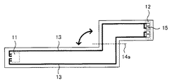
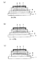
図1は、本発明のサスペンション用基板の一例を示す模式図である。図1(a)は本発明のサスペンション用基板の一例を示す概略平面図であり、図1(b)は図1(a)のA−A断面図である。なお、便宜上、図1(a)ではカバー層の記載は省略している。図1(a)に示されるサスペンション用基板20は、一方の先端部分に形成された素子実装領域11と、他方の先端部分に形成され、外部回路基板に接続するための外部回路基板接続領域12と、素子実装領域11および外部回路基板接続領域12を電気的に接続する配線層13とを有するものである。また、図1(a)における配線層13は、一方がライト用配線層であり、他方がリード用配線層である。また、上記の外部回路基板としては、例えば中継基板や、メインフレキシブル基板等が挙げられる。
FIG. 1 is a schematic view showing an example of a suspension substrate of the present invention. FIG. 1A is a schematic plan view showing an example of a suspension substrate according to the present invention, and FIG. 1B is a cross-sectional view taken along line AA in FIG. For convenience, the cover layer is not shown in FIG. A
一方、図1(b)に示すように、本発明のサスペンション用基板は、金属支持基板1と、金属支持基板1上に形成された第一絶縁層2と、第一絶縁層2上に形成された第一配線層3と、第一配線層3を覆うように形成された第二絶縁層4と、第二絶縁層4上に形成され、平面視上、第一配線層3と重複するように形成された第二配線層5と、第二配線層を覆うように形成されたカバー層6とを有するものである。第二絶縁層4を介して、第一配線層3および第二配線層5が積層されることにより、低インピーダンス化を図りやすくなるという利点がある。なお、第一配線層3および第二配線層5は、通常、差動配線である。
On the other hand, as shown in FIG. 1B, the suspension substrate of the present invention is formed on the
また、本発明のサスペンション用基板は、折り曲げ加工部において、カバー層が切れ込み部を有することを大きな特徴とする。折り曲げ加工部としては、例えば図1(a)における折り曲げ加工部14a〜14cを挙げることができる。これらの折り曲げ加工部については、後述する図4〜図6を用いて詳細に説明する。
The suspension substrate of the present invention is characterized in that the cover layer has a cut portion in the bent portion. As a bending process part, the bending
図2は、本発明における折り曲げ加工部を説明する模式図である。図2(a)は折り曲げ加工部を説明する概略平面図であり、図2(b)は図2(a)のA−A断面図である。図2(a)に示すように、本発明のサスペンション用基板は、折り曲げ加工部14において、カバー層6が切れ込み部10を有することを大きな特徴とする。なお、図2(b)では、第二配線層5が露出しているが、必要に応じて、後述する配線めっき層または薄肉層を形成することが好ましい。
FIG. 2 is a schematic diagram for explaining a bending portion in the present invention. FIG. 2A is a schematic plan view for explaining a bending portion, and FIG. 2B is a cross-sectional view taken along line AA in FIG. As shown in FIG. 2A, the suspension substrate of the present invention is characterized in that the
このように、本発明によれば、折り曲げ加工部において、カバー層が切れ込み部を有することから、一対の配線層を積層した厚いサスペンション用基板であっても、折り曲げ加工を行いやすくすることができる。その結果、折り曲げ加工を精度良く行うことができる。
以下、本発明のサスペンション用基板について、サスペンション用基板の部材と、サスペンション用基板の構成とに分けて説明する。
As described above, according to the present invention, since the cover layer has the cut portion in the bending portion, even if it is a thick suspension substrate in which a pair of wiring layers are stacked, the bending processing can be facilitated. . As a result, the bending process can be performed with high accuracy.
Hereinafter, the suspension substrate of the present invention will be described separately for the suspension substrate member and the suspension substrate configuration.
1.サスペンション用基板の部材
まず、本発明のサスペンション用基板の部材について説明する。本発明のサスペンション用基板は、金属支持基板、第一絶縁層、第一配線層、第二絶縁層、第二配線層およびカバー層を有するものである。
1. First, members of the suspension substrate of the present invention will be described. The suspension substrate of the present invention has a metal support substrate, a first insulating layer, a first wiring layer, a second insulating layer, a second wiring layer, and a cover layer.
本発明における金属支持基板は、サスペンション用基板の支持体として機能するものである。金属支持基板の材料は、ばね性を有する金属であることが好ましく、具体的にはSUS等を挙げることができる。また、金属支持基板の厚さは、その材料の種類により異なるものであるが、例えば10μm〜20μmの範囲内である。 The metal support substrate in the present invention functions as a support for the suspension substrate. The material of the metal support substrate is preferably a metal having spring properties, and specific examples include SUS. Moreover, although the thickness of a metal support substrate changes with kinds of the material, it exists in the range of 10 micrometers-20 micrometers, for example.
本発明における第一絶縁層は、金属支持基板上に形成されるものである。第一絶縁層の材料は、絶縁性を有するものであれば特に限定されるものではないが、例えば樹脂を挙げることができる。上記樹脂としては、例えばポリイミド樹脂、ポリベンゾオキサゾール樹脂、ポリベンゾイミダゾール樹脂、アクリル樹脂、ポリエーテルニトリル樹脂、ポリエーテルスルホン樹脂、ポリエチレンテレフタレート樹脂、ポリエチレンナフタレート樹脂およびポリ塩化ビニル樹脂を挙げることができ、中でもポリイミド樹脂が好ましい。絶縁性、耐熱性および耐薬品性に優れているからである。また、第一絶縁層の材料は、感光性材料であっても良く、非感光性材料であっても良い。第一絶縁層の厚さは、例えば5μm〜30μmの範囲内であることが好ましく、5μm〜18μmの範囲内であることがより好ましく、5μm〜12μmの範囲内であることがさらに好ましい。 The first insulating layer in the present invention is formed on a metal support substrate. The material of the first insulating layer is not particularly limited as long as it has insulating properties, and examples thereof include a resin. Examples of the resin include polyimide resin, polybenzoxazole resin, polybenzimidazole resin, acrylic resin, polyether nitrile resin, polyether sulfone resin, polyethylene terephthalate resin, polyethylene naphthalate resin, and polyvinyl chloride resin. Of these, polyimide resin is preferred. It is because it is excellent in insulation, heat resistance and chemical resistance. The material of the first insulating layer may be a photosensitive material or a non-photosensitive material. The thickness of the first insulating layer is, for example, preferably in the range of 5 μm to 30 μm, more preferably in the range of 5 μm to 18 μm, and still more preferably in the range of 5 μm to 12 μm.
本発明における第一配線層は、第一絶縁層上に形成されるものである。第一配線層の材料は、導電性を有するものであれば特に限定されるものではないが、例えば金属を挙げることができ、中でも銅(Cu)が好ましい。また、第一配線層の材料は、圧延銅であっても良く、電解銅であっても良い。第一配線層の厚さは、例えば5μm〜18μmの範囲内であることが好ましく、9μm〜12μmの範囲内であることがより好ましい。 The first wiring layer in the present invention is formed on the first insulating layer. The material of the first wiring layer is not particularly limited as long as it has conductivity, but for example, a metal can be used, and among these, copper (Cu) is preferable. The material of the first wiring layer may be rolled copper or electrolytic copper. The thickness of the first wiring layer is preferably in the range of 5 μm to 18 μm, for example, and more preferably in the range of 9 μm to 12 μm.
本発明における第二絶縁層は、第一配線層を覆うように形成されるものである。第二絶縁層の材料は、絶縁性を有するものであれば特に限定されるものではないが、例えば、上記の第一絶縁層の材料として記載したものを用いることができる。中でも、第二絶縁層の材料は、ポリイミド樹脂であることが好ましい。絶縁性、耐熱性および耐薬品性に優れているからである。また、第一配線層の頂面から第二配線層の底面までの第二絶縁層の厚さ(配線層間の第二絶縁層の厚さ)は、例えば5μm〜20μmの範囲内であることが好ましく、7μm〜15μmの範囲内であることがより好ましい。配線層間の第二絶縁層の厚さが小さすぎると、十分な絶縁性を発揮できない可能性があり、配線層間の第二絶縁層の厚さが大きすぎると、折り曲げ加工が精度良く行うことが困難になる可能性があるからである。 The second insulating layer in the present invention is formed so as to cover the first wiring layer. The material of the second insulating layer is not particularly limited as long as it has an insulating property, but for example, the material described as the material of the first insulating layer can be used. Especially, it is preferable that the material of a 2nd insulating layer is a polyimide resin. It is because it is excellent in insulation, heat resistance and chemical resistance. Further, the thickness of the second insulating layer (the thickness of the second insulating layer between the wiring layers) from the top surface of the first wiring layer to the bottom surface of the second wiring layer is, for example, in the range of 5 μm to 20 μm. Preferably, it is in the range of 7 μm to 15 μm. If the thickness of the second insulating layer between the wiring layers is too small, sufficient insulation may not be exhibited. If the thickness of the second insulating layer between the wiring layers is too large, the bending process may be performed with high accuracy. This may be difficult.
本発明における第二配線層は、第二絶縁層上に形成されるものである。第二配線層の材料は、導電性を有するものであれば特に限定されるものではないが、例えば、上記の第一配線層の材料として記載したものを用いることができる。中でも、第二配線層の材料は、銅(Cu)であることが好ましい。第二配線層の厚さの好ましい範囲は、上記の第一配線層の厚さの好ましい範囲と同様である。また、本発明における第二配線層は、平面視上、第一配線層に対して、少なくとも一部の領域で重複するように形成されているものである。中でも、第二配線層および第一配線層の平面視上の重複面積は、より多いことが好ましい。インピーダンスの設計が容易になるからである。特に、本発明においては、図1(b)に示すように、第一配線層3および第二配線層5の幅が、平面視上、一致していることが好ましい。
The second wiring layer in the present invention is formed on the second insulating layer. The material of the second wiring layer is not particularly limited as long as it has conductivity. For example, the material described as the material of the first wiring layer can be used. Especially, it is preferable that the material of a 2nd wiring layer is copper (Cu). The preferable range of the thickness of the second wiring layer is the same as the preferable range of the thickness of the first wiring layer. Further, the second wiring layer in the present invention is formed so as to overlap at least a part of the first wiring layer in plan view. Especially, it is preferable that there is more overlap area in planar view of a 2nd wiring layer and a 1st wiring layer. This is because impedance design is facilitated. In particular, in the present invention, as shown in FIG. 1B, it is preferable that the widths of the
本発明におけるカバー層は、第二配線層を覆うように形成されるものである。カバー層を設けることにより、第二配線層の劣化(腐食等)を防止できる。カバー層の材料としては、例えば、上述した第一絶縁層の材料として記載したものを挙げることができ、中でもポリイミド樹脂が好ましい。また、カバー層の材料は、感光性材料であっても良く、非感光性材料であっても良い。カバー層の厚さは、例えば2μm〜30μmの範囲内であることが好ましく、2μm〜10μmの範囲内であることがより好ましい。 The cover layer in the present invention is formed so as to cover the second wiring layer. By providing the cover layer, deterioration (corrosion or the like) of the second wiring layer can be prevented. Examples of the material of the cover layer include those described as the material of the first insulating layer described above, and among them, a polyimide resin is preferable. The material of the cover layer may be a photosensitive material or a non-photosensitive material. The thickness of the cover layer is preferably in the range of 2 μm to 30 μm, for example, and more preferably in the range of 2 μm to 10 μm.
2.サスペンション用基板の構成
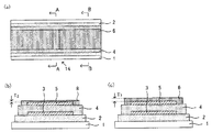
本発明のサスペンション用基板は、第一配線層および第二配線層を有し、この第二配線層を覆うカバー層に切れ込み部を有することを大きな特徴とする。第一配線層および第二配線層は、ライト用配線層であっても良く、リード用配線層であっても良いが、前者であることが好ましい。より低インピーダンス化が求められているからである。また、本発明のサスペンション用基板は、第一配線層および第二配線層の他に、第三配線層および第四配線層を有していても良い。すなわち、第一配線層および第二配線層を、ライト用配線層およびリード用配線層の一方とし、第三配線層および第四配線層を、ライト用配線層およびリード用配線層の他方としても良い。この場合、図3(a)に示すように、第三配線層21および第四配線層22は、ともに第一絶縁層2上に形成されたものであっても良く、図3(b)に示すように、第一絶縁層2上に第三配線層21が形成され、第二絶縁層4上に第四配線層22が形成されたものであっても良い。図3(a)の場合、第三配線層21および第四配線層22を覆うカバー層6は、折り曲げ加工部において、切れ込み部を有することが好ましい。また、第三配線層21および第四配線層22を覆うカバー層6は、第二配線層5を覆うカバー層6と同じ材料であっても良く、第一配線層3を覆う第二絶縁層4と同じ材料であっても良い。また、図3(b)の場合、第四配線層22を覆うカバー層6は、折り曲げ加工部において、切れ込み部を有していることが好ましい。なお、第三配線層および第四配線層の材料および厚さ等については、第一配線層および第二配線層と同様である。
2. Configuration of Suspension Substrate The suspension substrate of the present invention is characterized by having a first wiring layer and a second wiring layer, and having a cut portion in a cover layer covering the second wiring layer. The first wiring layer and the second wiring layer may be a write wiring layer or a read wiring layer, but the former is preferable. This is because lower impedance is required. The suspension substrate of the present invention may have a third wiring layer and a fourth wiring layer in addition to the first wiring layer and the second wiring layer. That is, the first wiring layer and the second wiring layer may be one of the write wiring layer and the read wiring layer, and the third wiring layer and the fourth wiring layer may be the other of the write wiring layer and the read wiring layer. good. In this case, as shown in FIG. 3A, both the
次に、本発明における折り曲げ加工部について説明する。本発明における折り曲げ加工部は、サスペンション用基板に対して、所定の角度を付与するように折り曲げ加工する部位であれば特に限定されるものではない。折り曲げ加工部の一例としては、図4に示す折り曲げ加工部14aを挙げることができる。この折り曲げ加工部14aは、端子部15を、外部回路基板(図示せず)に接続させるための折り曲げ加工部である。折り曲げ加工部14aを精度良く折り曲げることにより、外部回路基板との接続信頼性が向上するという利点がある。折り曲げ加工部14aの折り曲げる角度は、外部回路基板の位置によって異なるものであるが、例えば90°程度である。また、折り曲げ加工の方向は、配線層方向(図面の裏から表に向かう方向)であっても良く、金属支持基板方向(図面の表から裏に向かう方向)であっても良い。
Next, the bending process part in this invention is demonstrated. The bending part in the present invention is not particularly limited as long as it is a part that is bent so as to give a predetermined angle to the suspension substrate. As an example of the bent portion, a
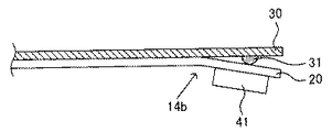
折り曲げ加工部の他の例としては、図5に示す折り曲げ加工部14bを挙げることができる。この折り曲げ加工部14bは、ディンプル31との組み合わせにより、サスペンション用基板に所定の弾性力を与え、磁気ヘッドスライダ等の素子41の遥動を制御するための折り曲げ加工部である。折り曲げ加工部14bを精度良く折り曲げることにより、遥動の制御を精密に行うことが可能になるという利点がある。折り曲げ加工部14bの折り曲げる角度は、ディンプルの大きさ等によって異なるものであるが、例えば0°より大きく40°未満の範囲内であり、0°より大きく30°未満の範囲内であることが好ましい。また、折り曲げ加工の方向は、通常、配線層方向(図面の下方向)である。
Another example of the bent portion is a
折り曲げ加工部のさらに他の例としては、ロードビームにばね性を付与するための折り曲げ部に対応した折り曲げ加工部を挙げることができる。具体的には、図6に示すように、ロードビーム30およびベースプレート32に連結したばね部材33に、折り曲げ部33aを設けることで、ロードビーム30にばね性を付与する場合は、その折り曲げ部33aに対応して、サスペンション用基板20に折り曲げ加工を行う必要がある。その部位が、サスペンション用基板20の折り曲げ加工部14cになる。折り曲げ加工部14cを精度良く折り曲げることにより、より安定したばね性を得ることができるという利点がある。折り曲げ加工部14cの折り曲げる角度は、対応する折り曲げ部の角度に応じて異なるものであるが、例えば0°より大きく30°未満の範囲内であり、0°より大きく25°未満の範囲内であることが好ましい。また、図6では、ばね部材33およびベースプレート32との境界も、折り曲げ加工部になっている。なお、図6では、ばね部材33に、折り曲げ部33aが形成されているが、その他の部材(例えばロードビーム自体)に折り曲げ部が形成されていても良い。その場合、その折り曲げ部に対応する部位が、サスペンション用基板の折り曲げ加工部になる。
As still another example of the bent portion, a bent portion corresponding to the bent portion for imparting spring property to the load beam can be cited. Specifically, as shown in FIG. 6, when the
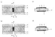
次に、本発明におけるカバー層の切れ込み部について説明する。カバー層の切れ込み部は、平面視上、折り曲げ加工部を含むように形成されたものであれば特に限定されるものではない。図7(a)においては、カバー層6が、平面視上、折り曲げ加工部14を含むように切れ込み部10を有している。この切れ込み部10は、カバー層の両端部に形成され、貫通しないタイプの切れ込み部である。一方、図7(b)においては、カバー層6が、一方の端部から他方の端部までを貫通する切れ込み部10を有している。貫通するタイプの切れ込み部は、貫通しないタイプの切れ込み部に比べて、より折り曲げ加工を行いやすくなるという利点を有する。切れ込み部10の幅W1は、特に限定されるものではないが、例えば5μm〜500μmの範囲内であることが好ましく、10μm〜100μmの範囲内であることが好ましい。W1の値が小さすぎると、安定した切れ込み加工が難しく、W1の値が大きすぎると、応力が広範囲に分散され、折り曲げ加工の精度が向上しなくなるからである。
Next, the notch part of the cover layer in this invention is demonstrated. The cut portion of the cover layer is not particularly limited as long as it is formed so as to include the bent portion in plan view. In FIG. 7A, the
図8は、本発明におけるカバー層の切れ込み部を説明する模式図である。図8(a)はカバー層の切れ込み部を説明する概略平面図であり、図8(b)は図8(a)のA−A断面図であり、図8(c)は図8(a)のB−B断面図である。図8(a)〜(c)に示すように、折り曲げ加工部14において、カバー層6から第二配線層5が露出する露出部が形成され、その露出部に配線めっき層7が形成されていることが好ましい。深い切れ込み部を設けることで、より折り曲げ加工を行いやすくすることができるからである。また、露出した配線層に配線めっき層を設けることにより、配線層の劣化を抑制することができる。配線めっき層としては、配線層を保護することができるものであれば特に限定されるものではないが、例えば、ニッケルめっき層および金めっき層等を挙げることができる。また、配線めっき層は、複数の金属めっき層からなるものであっても良い。第二配線層5上に形成された配線めっき層7の厚さT1は、例えば0.1μm〜5.0μmの範囲内であることが好ましい。
FIG. 8 is a schematic view for explaining a cut portion of the cover layer in the present invention. FIG. 8A is a schematic plan view for explaining a cut portion of the cover layer, FIG. 8B is a cross-sectional view taken along line AA of FIG. 8A, and FIG. 8C is FIG. It is BB sectional drawing of). As shown in FIGS. 8A to 8C, in the
図9は、本発明におけるカバー層の切れ込み部を説明する模式図である。図9(a)はカバー層の切れ込み部を説明する概略平面図であり、図9(b)は図9(a)のA−A断面図であり、図9(c)は図9(a)のB−B断面図である。図9(a)〜(c)に示すように、折り曲げ加工部14において、カバー層6よりも厚さの薄い薄肉層8が形成されていることが好ましい。配線めっき層を設けることなく、より折り曲げ加工を行いやすくすることができるからである。薄肉層8は、カバー層6と同一の材料であることが好ましい。また、薄肉層8は、例えばカバー層6をエッチングすることにより形成することができる。第二配線層5上に形成された薄肉層8の厚さT2は、例えば0.4μm〜3.2μmの範囲内であることが好ましく、1.2μm〜2.4μmの範囲内であることがより好ましい。薄肉層の厚さが小さすぎると、ピンホール等によって第二配線層が露出し、第二配線層の劣化を引き起こす可能性があり、薄肉層の厚さが大きすぎると、折り曲げ加工を行いやすくすることができない可能性があるからである。また、カバー層6の厚さT3に対する、薄肉層8の厚さT2の割合(T2/T3)は、例えば10%〜80%の範囲内であることが好ましく、30%〜60%の範囲内であることがより好ましい。
FIG. 9 is a schematic view for explaining a cut portion of the cover layer in the present invention. FIG. 9A is a schematic plan view for explaining a cut portion of the cover layer, FIG. 9B is a cross-sectional view taken along line AA of FIG. 9A, and FIG. 9C is FIG. It is BB sectional drawing of). As shown in FIGS. 9A to 9C, it is preferable that a thin layer 8 having a thickness smaller than that of the
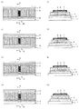
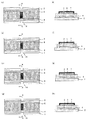
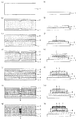
次に、折り曲げ加工部におけるサスペンション用基板の構成について説明する。図10は、折り曲げ加工部におけるサスペンション用基板の構成の一例を説明する模式図である。図10(e)、(f)、(g)、(h)は、それぞれ、図10(a)、(b)、(c)、(d)のA−A断面図である。図10(a)、(e)に示すように、本発明のサスペンション用基板は、折り曲げ加工部14において、金属支持基板1、第一絶縁層2、第一配線層3、第二絶縁層4および第二配線層5が存在することが好ましい。この形態を第一の形態とする。
Next, the configuration of the suspension substrate in the bent portion will be described. FIG. 10 is a schematic diagram for explaining an example of the configuration of the suspension substrate in the bending portion. FIGS. 10E, 10F, 10G, and 10H are cross-sectional views taken along line AA in FIGS. 10A, 10B, 10C, and 10D, respectively. As shown in FIGS. 10A and 10E, the suspension substrate of the present invention has a
第一の形態では、図10(b)、(f)に示すように、折り曲げ加工部14において、第二絶縁層4が切れ込み部を有することが好ましい。第二絶縁層4が切れ込み部を有することで、より折り曲げ加工を行いやすくすることができるからである。また、第二絶縁層4は、第一配線層3および第二配線層5を絶縁する必要があるため、ある程度の厚さが必要となる。そのため、その第二絶縁層に切れ込み部を設けることで、折り曲げ加工を行いやすくなる。
In the first embodiment, as shown in FIGS. 10B and 10F, it is preferable that the second insulating
また、第一の形態では、図10(c)、(g)に示すように、折り曲げ加工部14において、第一絶縁層2が切れ込み部を有することが好ましい。第一絶縁層2が切れ込み部を有することで、より折り曲げ加工を行いやすくすることができるからである。特に、第一の形態では、図10(d)、(h)に示すように、折り曲げ加工部14において、第二絶縁層4および第一絶縁層2が、それぞれ切れ込み部を有することが好ましい。
In the first embodiment, as shown in FIGS. 10C and 10G, it is preferable that the first insulating
ここで、第二絶縁層および第一絶縁層の切れ込み部は、それぞれ、平面視上、折り曲げ加工部を含むように形成されたものであれば特に限定されるものではない。図11(a)は、図10(f)と同様に、第二絶縁層4が切れ込み部を有するものである。図11(a)に示すように、第二絶縁層4の端部と第一配線層3の端部との幅をW2とした場合、W2は10μm以上であることが好ましく、10μm〜30μmの範囲内であることが好ましい。W2の値が小さすぎると、第二絶縁層のピンホールによる第一配線層の露出で配線層の劣化やショートを招き、W2の値が大きすぎると、折り曲げ加工を行いやすくする目的が達成しにくくなるからである。なお、図11(a)では、第一配線層3の端部と第二配線層5の端部とが一致した場合を示しているが、もし、第二配線層5の端部が、第一配線層3の端部よりも外側にある場合は、第二配線層5の端部と、第二絶縁層4の端部との幅(W2´)が、上記範囲にあることが好ましい。
Here, the cut portions of the second insulating layer and the first insulating layer are not particularly limited as long as they are formed so as to include a bent portion in plan view. FIG. 11A shows a case where the second insulating
一方、図11(b)は、図10(g)と同様に、第一絶縁層2が切れ込み部を有するものである。図11(b)に示すように、第一絶縁層2の端部と第一配線層3の端部との幅をW3とした場合、W3は10μm以上であることが好ましく、10μm〜30μmの範囲内であることが好ましい。W3の値が小さすぎると、第二絶縁層のピンホールによる第一配線層の露出で配線層の劣化やショートを招き、W3の値が大きすぎると、折り曲げ加工を行いやすくする目的が達成しにくくなるからである。なお、図11(b)では、第一配線層3の端部と第二配線層5の端部とが一致した場合を示しているが、もし、第二配線層5の端部が、第一配線層3の端部よりも外側にある場合は、第二配線層5の端部と、第一絶縁層2の端部との幅(W3´)が、上記範囲にあることが好ましい。また、本発明においては、図11(c)に示すように、第一絶縁層2の端部と、第二絶縁層4の端部とが一致していても良い。
On the other hand, in FIG. 11B, the first insulating
図12は、折り曲げ加工部におけるサスペンション用基板の構成の他の例を説明する模式図である。図12(e)、(f)、(g)、(h)は、それぞれ、図12(a)、(b)、(c)、(d)のA−A断面図である。図12(a)、(e)に示すように、本発明のサスペンション用基板は、折り曲げ加工部14において、第一絶縁層2、第一配線層3、第二絶縁層4および第二配線層5が存在し、金属支持基板1が存在しないことが好ましい。金属支持基板を除去することにより、より折り曲げ加工を行いやすくなるからである。この形態を第二の形態とする。
FIG. 12 is a schematic diagram for explaining another example of the configuration of the suspension substrate in the bending portion. FIGS. 12E, 12F, 12G, and 12H are cross-sectional views taken along line AA in FIGS. 12A, 12B, 12C, and 12D, respectively. As shown in FIGS. 12A and 12E, the suspension substrate of the present invention includes a first insulating
第二の形態では、第一の形態と同様に、折り曲げ加工部14において、第二絶縁層4が切れ込み部を有していても良く(図12(b)、(f))、第一絶縁層2が切れ込み部を有していても良く(図12(c)、(g))、第二絶縁層4および第一絶縁層2が切れ込み部を有していても良い(図12(d)、(h))。また、特に第二の形態は、上記図1の折り曲げ加工部14aに適用されていることが好ましい。通常、折り曲げる角度が大きいからである。また、第二の形態は、折り曲げ加工部において、金属支持基板が存在しないことを一つの特徴とするが、折り曲げ加工部において、平面視上、第一配線層および第二配線層と重複する位置の金属支持基板が、少なくとも存在しないことが好ましい。なお、折り曲げ加工部の全体に渡って、金属支持基板が存在しなくても良い。
In the second embodiment, similarly to the first embodiment, the second insulating
図13は、折り曲げ加工部におけるサスペンション用基板の構成のさらに他の例を説明する模式図である。図13(c)、(d)は、それぞれ、図13(a)、(b)のA−A断面図である。図13(a)、(c)に示すように、本発明のサスペンション用基板は、折り曲げ加工部14において、第一配線層3、第二絶縁層4および第二配線層5が存在し、金属支持基板1および第一絶縁層2が存在しないことが好ましい。金属支持基板および第一絶縁層を除去することにより、より折り曲げ加工を行いやすくなるからである。この形態を第三の形態とする。
FIG. 13 is a schematic diagram illustrating still another example of the configuration of the suspension substrate in the bending portion. FIGS. 13C and 13D are cross-sectional views taken along lines AA in FIGS. 13A and 13B, respectively. As shown in FIGS. 13A and 13C, the suspension substrate of the present invention includes the
第三の形態では、第一の形態と同様に、折り曲げ加工部14において、第二絶縁層4が切れ込み部を有していても良い(図13(b)、(d))。特に第三の形態は、上記図1の折り曲げ加工部14aに適用されていることが好ましい。通常、折り曲げる角度が大きいからである。また、第三の形態は、折り曲げ加工部において、金属支持基板および第一絶縁層が存在しないことを一つの特徴とするが、折り曲げ加工部において、平面視上、第一配線層および第二配線層と重複する位置の金属支持基板および第一絶縁層が、少なくとも存在しないことが好ましい。なお、折り曲げ加工部の全体に渡って、金属支持基板がおよび第一絶縁層が存在しなくても良い。また、第三の形態においては、図13(c)、(d)に示すように、第一配線層3の表面に配線めっき層7が形成されていることが好ましい。第一配線層3の劣化を防止できるからである。
In the third embodiment, similarly to the first embodiment, the second insulating
B.サスペンション
次に、本発明のサスペンションについて説明する。本発明のサスペンションは、上述したサスペンション用基板を含むことを特徴とするものである。
B. Suspension Next, the suspension of the present invention will be described. The suspension of the present invention includes the above-described suspension substrate.
図14は、本発明のサスペンションの一例を示す概略平面図である。図14に示されるサスペンション40は、上述したサスペンション用基板20と、素子実装領域11が形成されている表面とは反対側のサスペンション用基板20の表面に備え付けられたロードビーム30とを有するものである。
FIG. 14 is a schematic plan view showing an example of the suspension of the present invention. A
本発明によれば、上述したサスペンション用基板を用いることで、サスペンション用基板の折り曲げ精度の良いサスペンションとすることができる。 According to the present invention, by using the above-described suspension substrate, the suspension substrate can be a suspension with high bending accuracy.
本発明のサスペンションは、少なくともサスペンション用基板を有し、通常は、さらにロードビームを有する。サスペンション用基板については、上記「A.サスペンション用基板」に記載した内容と同様であるので、ここでの記載は省略する。また、ロードビームは、一般的なサスペンションに用いられるロードビームと同様のものを用いることができる。また、本発明のサスペンションに含まれるサスペンション用基板は、折り曲げ加工されたものであっても良い。 The suspension of the present invention has at least a suspension substrate, and usually further has a load beam. The suspension substrate is the same as the content described in “A. Suspension substrate”, and therefore, the description thereof is omitted here. The load beam can be the same as the load beam used for a general suspension. Further, the suspension substrate included in the suspension of the present invention may be bent.
C.素子付サスペンション
次に、本発明の素子付サスペンションについて説明する。本発明の素子付サスペンションは、上述したサスペンションと、上記サスペンションに実装された素子とを有するものである。
C. Next, the suspension with an element of the present invention will be described. The suspension with an element of the present invention includes the above-described suspension and an element mounted on the suspension.
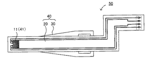
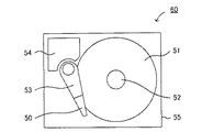
図15は、本発明の素子付サスペンションの一例を示す概略平面図である。図15に示される素子付サスペンション50は、上述したサスペンション40と、サスペンション40の素子実装領域11に実装された素子41とを有するものである。
FIG. 15 is a schematic plan view showing an example of the suspension with an element of the present invention. A
本発明によれば、上述したサスペンションを用いることで、サスペンション用基板の折り曲げ精度の良い素子付サスペンションとすることができる。 According to the present invention, by using the above-described suspension, it is possible to provide a suspension with an element with high folding accuracy of the suspension substrate.
本発明の素子付サスペンションは、少なくともサスペンションおよび素子を有するものである。サスペンションについては、上記「B.サスペンション」に記載した内容と同様であるので、ここでの記載は省略する。また、素子実装領域に実装される素子としては、例えば、磁気ヘッドスライダ、アクチュエータ、半導体等を挙げることができる。また、上記アクチュエータは、磁気ヘッドを有するものであっても良く、磁気ヘッドを有しないものであっても良い。また、本発明の素子付サスペンションに含まれるサスペンション用基板は、折り曲げ加工されたものであっても良い。 The suspension with an element of the present invention has at least a suspension and an element. The suspension is the same as that described in “B. Suspension” above, and is not described here. In addition, examples of elements mounted in the element mounting area include a magnetic head slider, an actuator, and a semiconductor. The actuator may have a magnetic head or may not have a magnetic head. The suspension substrate included in the element-equipped suspension of the present invention may be bent.
D.ハードディスクドライブ
次に、本発明のハードディスクドライブについて説明する。本発明のハードディスクドライブは、上述した素子付サスペンションを含むことを特徴とするものである。
D. Next, the hard disk drive of the present invention will be described. The hard disk drive of the present invention is characterized by including the above-described suspension with an element.
図16は、本発明のハードディスクドライブの一例を示す概略平面図である。図16に示されるハードディスクドライブ60は、上述した素子付サスペンション50と、素子付サスペンション50がデータの書き込みおよび読み込みを行うディスク51と、ディスク51を回転させるスピンドルモータ52と、素子付サスペンション50の素子を移動させるアーム53およびボイスコイルモータ54と、上記の部材を密閉するケース55とを有するものである。
FIG. 16 is a schematic plan view showing an example of the hard disk drive of the present invention. The
本発明によれば、上述した素子付サスペンションを用いることで、高性能なハードディスクドライブとすることができる。 According to the present invention, a high-performance hard disk drive can be obtained by using the above-described suspension with an element.
本発明のハードディスクドライブは、少なくとも素子付サスペンションを有し、通常は、さらにディスク、スピンドルモータ、アームおよびボイスコイルモータを有する。素子付サスペンションについては、上記「C.素子付サスペンション」に記載した内容と同様であるので、ここでの記載は省略する。また、その他の部材についても、一般的なハードディスクドライブに用いられる部材と同様のものを用いることができる。 The hard disk drive of the present invention has at least a suspension with an element, and usually further includes a disk, a spindle motor, an arm, and a voice coil motor. Since the suspension with an element is the same as the content described in “C. Suspension with an element”, description thereof is omitted here. As other members, the same members as those used in a general hard disk drive can be used.
E.サスペンション用基板の製造方法
次に、本発明のサスペンション用基板の製造方法について説明する。本発明のサスペンション用基板の製造方法は、金属支持基板と、上記金属支持基板上に形成された第一絶縁層と、上記第一絶縁層上に形成された第一配線層と、上記第一配線層を覆うように形成された第二絶縁層と、上記第二絶縁層上に形成され、平面視上、上記第一配線層と重複するように形成された第二配線層と、上記第二配線層を覆うように形成されたカバー層とを有するサスペンション用基板の製造方法であって、折り曲げ加工部において、切れ込み部を有する上記カバー層を形成するカバー層形成工程を有することを特徴とするものである。
E. Next, a method for manufacturing a suspension substrate according to the present invention will be described. The manufacturing method of the suspension substrate of the present invention includes a metal support substrate, a first insulating layer formed on the metal support substrate, a first wiring layer formed on the first insulating layer, and the first A second insulating layer formed so as to cover the wiring layer; a second wiring layer formed on the second insulating layer so as to overlap the first wiring layer in plan view; A method of manufacturing a suspension substrate having a cover layer formed so as to cover two wiring layers, comprising a cover layer forming step of forming the cover layer having a cut portion in a bent portion. To do.
図17は、本発明のサスペンション用基板の製造方法の一例を示す模式図である。なお、図17(h)、(i)、(j)、(k)、(l)、(m)、(n)は、それぞれ図17(a)、(b)、(c)、(d)、(e)、(f)、(g)の折り曲げ加工部の断面図である。図17に示されるサスペンション用基板の製造方法においては、まず、金属支持基板1(例えばステンレススティール)を用意する(図17(a)、(h))。次に、金属支持基板1の表面に、ポリイミドを塗布、加工することによって、第一絶縁層2を形成する(図17(b)、(i))。この際、折り曲げ加工部となる位置の第一絶縁層2に、切れ込み部を形成する。次に、第一絶縁層2の表面に、スパッタリング法により拡散防止層(例えばCr薄膜層)およびシード層(例えばCu薄膜層)を形成する。その後、シード層が形成された表面に、所定のレジストパターンを形成し、電解めっき法により、第一配線層3を形成する(図17(c)、(j))。
FIG. 17 is a schematic view showing an example of a method for manufacturing a suspension substrate according to the present invention. 17 (h), (i), (j), (k), (l), (m), and (n) are respectively shown in FIGS. 17 (a), (b), (c), and (d). It is sectional drawing of the bending process part of (), (e), (f), (g). In the method for manufacturing a suspension substrate shown in FIG. 17, first, a metal support substrate 1 (for example, stainless steel) is prepared (FIGS. 17A and 17H). Next, the first insulating
その後、不要なレジストパターン、拡散防止層およびシード層を除去し、第一配線層3が形成されている側の基板表面に、ポリイミドを塗布、加工することによって第二絶縁層4を形成する(図17(d)、(k))。この際、折り曲げ加工部となる位置の第二絶縁層4に、切れ込み部を形成する。次に、第二絶縁層4の表面に、スパッタリング法により拡散防止層(例えばCr薄膜層)およびシード層(例えばCu薄膜層)を形成する。その後、シード層が形成された表面に、所定のレジストパターンを形成し、電解めっき法により、第二配線層5を形成する(図17(e)、(l))。
Then, an unnecessary resist pattern, a diffusion prevention layer, and a seed layer are removed, and a second
次に、第二絶縁層4および第二配線層5の表面に、ポリイミドを塗布、加工することによって、カバー層6を形成する(図17(f)、(m))。この際、折り曲げ加工部となる位置のカバー層6に、切れ込み部を形成する。最後に、切れ込み部15において露出する第二配線層5の表面に、NiめっきおよびAuめっきを行うことにより、配線めっき層7を形成し、本発明のサスペンション用基板を得る(図17(g)、(n))。
Next, a
なお、図17では、金属支持基板からサスペンション用基板の形成を行ったが、例えば、金属支持基板と、第一絶縁層を形成するための絶縁層と、第一配線層を形成するための導体層とからなる積層材(三層材)を用いてサスペンション用基板の形成を行っても良い。 In FIG. 17, the suspension substrate is formed from the metal support substrate. For example, the metal support substrate, the insulating layer for forming the first insulating layer, and the conductor for forming the first wiring layer are used. The suspension substrate may be formed using a laminated material (three-layer material) made of layers.
このように、本発明によれば、折り曲げ加工部において、切れ込み部を有するカバー層を形成することにより、一対の配線層を積層した厚いサスペンション用基板であっても、折り曲げ加工を行いやすいサスペンション用基板を得ることができる。 As described above, according to the present invention, even in the case of a thick suspension substrate in which a pair of wiring layers are stacked by forming a cover layer having a cut portion in a bent portion, the suspension is easy to be bent. A substrate can be obtained.
本発明におけるカバー層形成工程は、折り曲げ加工部において、切れ込み部を有するカバー層を形成する工程である。本発明において、カバー層の切れ込み部の形成方法は特に限定されるものではないが、その一例としては、折り曲げ加工部を覆うカバー層を形成し、その後、折り曲げ加工部のカバー層が露出するレジストパターンを形成し、露出するカバー層をウェットエッチングする方法を挙げることができる。また、例えばカバー層の材料が光硬化性材料である場合は、切れ込み部を形成する位置のカバー層を硬化させないことにより、切れ込み部を形成することもできる。また、上述した薄肉層は、ウェットエッチングの条件を適宜変更したり、照射する光の量を調整したりすることで、形成することができる。 The cover layer forming step in the present invention is a step of forming a cover layer having a cut portion in the bent portion. In the present invention, the method of forming the cut portion of the cover layer is not particularly limited, but as an example, a resist that forms a cover layer that covers the bent portion and then exposes the cover layer of the bent portion. A method of forming a pattern and wet-etching the exposed cover layer can be mentioned. For example, when the material of the cover layer is a photocurable material, the cut portion can be formed by not curing the cover layer at the position where the cut portion is formed. The thin layer described above can be formed by appropriately changing the wet etching conditions or adjusting the amount of light to be irradiated.
また、本発明においては、第一絶縁層および第二絶縁層の少なくとも一方に、切れ込み部を形成しても良い。切れ込み部の形成方法は特に限定されるものではなく、通常のウェットエッチングやフォトリソグラフィーにより形成することができる。また、本発明においては、カバー層の切れ込み部で露出する第二配線層に配線めっき層を形成するめっき工程を有していても良い。 In the present invention, a cut portion may be formed in at least one of the first insulating layer and the second insulating layer. The method for forming the cut portion is not particularly limited, and can be formed by ordinary wet etching or photolithography. Moreover, in this invention, you may have the plating process which forms a wiring plating layer in the 2nd wiring layer exposed by the notch part of a cover layer.
なお、本発明は、上記実施形態に限定されるものではない。上記実施形態は例示であり、本発明の特許請求の範囲に記載された技術的思想と、実質的に同一の構成を有し、同様な作用効果を奏するものは、いかなる場合であっても本発明の技術的範囲に包含される。 The present invention is not limited to the above embodiment. The above-described embodiment is an exemplification, and the technical idea described in the claims of the present invention has substantially the same configuration and exhibits the same function and effect regardless of the case. It is included in the technical scope of the invention.
1…金属支持基板、2…第一絶縁層、3…第一配線層、4…第二絶縁層、5…第二配線層、6…カバー層、7…配線めっき層、8…薄肉層、10…切れ込み部、11…素子実装領域、12…外部回路基板接続領域、13…配線層、14…折り曲げ加工部、15…端子部、20…サスペンション用基板、21…第三配線層、22…第四配線層、30…ロードビーム、31…ディンプル、32…ベースプレート、33…ばね部材、40…サスペンション、41…素子、50…素子サスペンション、51…ディスク、52…スピンドルモータ、53…アーム、54…ボイスコイルモータ、55…ケース、60…ハードディスクドライブ
DESCRIPTION OF
Claims (16)
折り曲げ加工部において、前記カバー層は、切れ込み部を有し、
前記折り曲げ加工部において、前記カバー層から前記第二配線層が露出する露出部が形成され、前記露出部に配線めっき層が形成されていることを特徴とするサスペンション用基板。 A metal support substrate, a first insulating layer formed on the metal support substrate, a first wiring layer formed on the first insulating layer, and a second formed so as to cover the first wiring layer An insulating layer; a second wiring layer formed on the second insulating layer so as to overlap the first wiring layer in plan view; and a cover formed to cover the second wiring layer A suspension substrate having a layer,
In bending section, the cover layer may have a cut portion,
The suspension substrate according to claim 1, wherein an exposed portion where the second wiring layer is exposed from the cover layer is formed in the bent portion, and a wiring plating layer is formed on the exposed portion .
前記折り曲げ加工部において、前記切れ込み部を有する前記カバー層を形成するカバー層形成工程を有することを特徴とするサスペンション用基板の製造方法。 A metal support substrate, a first insulating layer formed on the metal support substrate, a first wiring layer formed on the first insulating layer, and a second formed so as to cover the first wiring layer An insulating layer; a second wiring layer formed on the second insulating layer so as to overlap the first wiring layer in plan view; and a cover formed to cover the second wiring layer possess a layer, the bent portion, wherein the cover layer has a notch, in the bent portion, the exposed portion is formed to the second wiring layer is exposed from the cover layer, the exposed portion A method for manufacturing a suspension substrate on which a wiring plating layer is formed ,
A method of manufacturing a suspension substrate, comprising: a cover layer forming step of forming the cover layer having the cut portion in the bent portion.
Priority Applications (1)
| Application Number | Priority Date | Filing Date | Title |
|---|---|---|---|
| JP2011007920A JP5772002B2 (en) | 2011-01-18 | 2011-01-18 | Suspension substrate, suspension, suspension with element, hard disk drive, and method for manufacturing suspension substrate |
Applications Claiming Priority (1)
| Application Number | Priority Date | Filing Date | Title |
|---|---|---|---|
| JP2011007920A JP5772002B2 (en) | 2011-01-18 | 2011-01-18 | Suspension substrate, suspension, suspension with element, hard disk drive, and method for manufacturing suspension substrate |
Publications (2)
| Publication Number | Publication Date |
|---|---|
| JP2012150861A JP2012150861A (en) | 2012-08-09 |
| JP5772002B2 true JP5772002B2 (en) | 2015-09-02 |
Family
ID=46792976
Family Applications (1)
| Application Number | Title | Priority Date | Filing Date |
|---|---|---|---|
| JP2011007920A Expired - Fee Related JP5772002B2 (en) | 2011-01-18 | 2011-01-18 | Suspension substrate, suspension, suspension with element, hard disk drive, and method for manufacturing suspension substrate |
Country Status (1)
| Country | Link |
|---|---|
| JP (1) | JP5772002B2 (en) |
Families Citing this family (3)
| Publication number | Priority date | Publication date | Assignee | Title |
|---|---|---|---|---|
| JP6511371B2 (en) * | 2015-09-10 | 2019-05-15 | 日本発條株式会社 | Flexure of suspension for disk drive and manufacturing method of wiring portion of flexure |
| JP6660185B2 (en) * | 2016-01-07 | 2020-03-11 | 日本発條株式会社 | Thin wiring board |
| JP6945994B2 (en) * | 2016-12-05 | 2021-10-06 | 株式会社ジャパンディスプレイ | Display device |
Family Cites Families (5)
| Publication number | Priority date | Publication date | Assignee | Title |
|---|---|---|---|---|
| JPH0217879U (en) * | 1988-07-21 | 1990-02-06 | ||
| JPH0922570A (en) * | 1995-07-03 | 1997-01-21 | Fujitsu Ltd | Head assembly and magnetic disk device including the head assembly |
| JP2001111178A (en) * | 1999-10-13 | 2001-04-20 | Nitto Denko Corp | Flexible wiring board |
| US7092214B2 (en) * | 2001-08-28 | 2006-08-15 | Sae Magnetics (H.K.) Ltd. | Wireless suspension design to accommodate multiple drive designs |
| JP4019068B2 (en) * | 2004-05-10 | 2007-12-05 | 日東電工株式会社 | Suspension board with circuit |
-
2011
- 2011-01-18 JP JP2011007920A patent/JP5772002B2/en not_active Expired - Fee Related
Also Published As
| Publication number | Publication date |
|---|---|
| JP2012150861A (en) | 2012-08-09 |
Similar Documents
| Publication | Publication Date | Title |
|---|---|---|
| JP5604850B2 (en) | Suspension board, suspension, suspension with head and hard disk drive | |
| JP2010170647A (en) | Suspension substrate, suspension, suspension with head, and hard disk drive | |
| JP5195956B2 (en) | Suspension board, suspension, suspension with element, and hard disk drive | |
| JP2011198402A (en) | Flexure substrate for suspension, suspension, suspension with head, and hard disk drive | |
| JP5772002B2 (en) | Suspension substrate, suspension, suspension with element, hard disk drive, and method for manufacturing suspension substrate | |
| JP5966287B2 (en) | Suspension substrate, suspension, suspension with element, hard disk drive, and manufacturing method of suspension substrate | |
| JP5817594B2 (en) | Suspension board with test pad, suspension board, suspension, suspension with element, and hard disk drive | |
| JP5218022B2 (en) | Suspension board, suspension, suspension with head and hard disk drive | |
| JP5870496B2 (en) | Flexure substrate for suspension, suspension, suspension with head, and hard disk drive | |
| JP5966296B2 (en) | Flexure substrate for suspension, suspension, suspension with head, and hard disk drive | |
| JP6160169B2 (en) | Suspension board, suspension, suspension with element, and hard disk drive | |
| JP2012123864A (en) | Flexure substrate for suspension, suspension, suspension with head, and hard disk drive | |
| JP5131604B2 (en) | Suspension substrate and method for manufacturing suspension substrate | |
| JP6037216B2 (en) | Flexure substrate for suspension | |
| JP5131605B2 (en) | Suspension board | |
| JP6160756B2 (en) | Flexure substrate for suspension, suspension, suspension with head, and hard disk drive | |
| JP2014199701A (en) | Substrate for suspension, suspension, suspension having element and hard disk | |
| JP6135171B2 (en) | Suspension board, suspension, suspension with element, and hard disk drive | |
| JP6024803B2 (en) | Flexure substrate for suspension, suspension, suspension with head, and hard disk drive | |
| JP5810570B2 (en) | Flexure substrate for suspension, suspension, suspension with head, and hard disk drive | |
| JP6123843B2 (en) | Flexure substrate for suspension, suspension, suspension with head, and hard disk drive | |
| JP5793897B2 (en) | Suspension substrate, suspension, suspension with element, hard disk drive, and manufacturing method of suspension substrate | |
| JP6070881B2 (en) | Suspension substrate, suspension, suspension with element, hard disk drive, and manufacturing method of suspension substrate | |
| JP6092505B2 (en) | Suspension substrate, suspension, suspension with element, hard disk drive, and manufacturing method of suspension substrate | |
| JP6174843B2 (en) | Suspension substrate, suspension, suspension with element, hard disk drive, and manufacturing method of suspension substrate |
Legal Events
| Date | Code | Title | Description |
|---|---|---|---|
| A621 | Written request for application examination |
Free format text: JAPANESE INTERMEDIATE CODE: A621 Effective date: 20131118 |
|
| A977 | Report on retrieval |
Free format text: JAPANESE INTERMEDIATE CODE: A971007 Effective date: 20140916 |
|
| A131 | Notification of reasons for refusal |
Free format text: JAPANESE INTERMEDIATE CODE: A131 Effective date: 20140924 |
|
| A521 | Written amendment |
Free format text: JAPANESE INTERMEDIATE CODE: A523 Effective date: 20141125 |
|
| TRDD | Decision of grant or rejection written | ||
| A01 | Written decision to grant a patent or to grant a registration (utility model) |
Free format text: JAPANESE INTERMEDIATE CODE: A01 Effective date: 20150602 |
|
| A61 | First payment of annual fees (during grant procedure) |
Free format text: JAPANESE INTERMEDIATE CODE: A61 Effective date: 20150615 |
|
| R150 | Certificate of patent or registration of utility model |
Ref document number: 5772002 Country of ref document: JP Free format text: JAPANESE INTERMEDIATE CODE: R150 |
|
| LAPS | Cancellation because of no payment of annual fees |