JP5771968B2 - Manufacturing method of semiconductor device, laminated support substrate for epitaxial growth, and laminated support substrate for device - Google Patents

Manufacturing method of semiconductor device, laminated support substrate for epitaxial growth, and laminated support substrate for device Download PDF

Info

Publication number
JP5771968B2
JP5771968B2 JP2010275893A JP2010275893A JP5771968B2 JP 5771968 B2 JP5771968 B2 JP 5771968B2 JP 2010275893 A JP2010275893 A JP 2010275893A JP 2010275893 A JP2010275893 A JP 2010275893A JP 5771968 B2 JP5771968 B2 JP 5771968B2
Authority
JP
Japan
Prior art keywords
layer
support substrate
transparent
laminated
gan
Prior art date
Legal status (The legal status is an assumption and is not a legal conclusion. Google has not performed a legal analysis and makes no representation as to the accuracy of the status listed.)
Active
Application number
JP2010275893A
Other languages
Japanese (ja)
Other versions
JP2011233861A (en
Inventor
邦亮 石原
邦亮 石原
昭広 八郷
昭広 八郷
松原 秀樹
秀樹 松原
Current Assignee (The listed assignees may be inaccurate. Google has not performed a legal analysis and makes no representation or warranty as to the accuracy of the list.)
Sumitomo Electric Industries Ltd
Original Assignee
Sumitomo Electric Industries Ltd
Priority date (The priority date is an assumption and is not a legal conclusion. Google has not performed a legal analysis and makes no representation as to the accuracy of the date listed.)
Filing date
Publication date
Application filed by Sumitomo Electric Industries Ltd filed Critical Sumitomo Electric Industries Ltd
Priority to JP2010275893A priority Critical patent/JP5771968B2/en
Publication of JP2011233861A publication Critical patent/JP2011233861A/en
Application granted granted Critical
Publication of JP5771968B2 publication Critical patent/JP5771968B2/en
Active legal-status Critical Current
Anticipated expiration legal-status Critical

Links

Images

Description

本発明は、半導体デバイスの製造方法、ならびにその製造方法において製造されるエピ成長用積層支持基板およびデバイス用積層支持基板に関する。   The present invention relates to a method for manufacturing a semiconductor device, a laminated support substrate for epitaxial growth manufactured by the manufacturing method, and a stacked support substrate for a device.

青色発光デバイスなどのIII族窒化物系半導体デバイスを製造するための基板としては、発光層となる良質のIII族窒化物系半導体層をエピタキシャル成長させる観点から、格子定数および熱膨張係数がIII族窒化物系半導体層に近似しているGaN基板が好適に用いられる。   As a substrate for manufacturing a group III nitride semiconductor device such as a blue light emitting device, a lattice constant and a thermal expansion coefficient are group III nitride from the viewpoint of epitaxially growing a high-quality group III nitride semiconductor layer serving as a light emitting layer. A GaN substrate that approximates a physical semiconductor layer is preferably used.

かかるGaN基板は非常に高価であるため、特開2006−210660号公報(以下、引用文献1という)および特開2008−300562号公報(以下、引用文献2という)において、シリコン(Si)基板、サファイア基板などのGaN以外の支持基板上に膜厚の小さいGaN層を貼り合わせた基板およびその製造方法が提案されている。   Since such a GaN substrate is very expensive, in Japanese Unexamined Patent Application Publication No. 2006-210660 (hereinafter referred to as Reference Document 1) and Japanese Unexamined Patent Application Publication No. 2008-300562 (hereinafter referred to as Reference Document 2), a silicon (Si) substrate, A substrate in which a GaN layer having a small film thickness is bonded onto a support substrate other than GaN such as a sapphire substrate and a method for manufacturing the same have been proposed.

特開2006−210660号公報JP 2006-210660 A 特開2008−300562号公報JP 2008-300562 A

しかし、上記の特開2006−210660号公報(引用文献1)および特開2008−300562号公報(引用文献2)で提案された上記貼り合わせ基板を用いても、GaN以外の支持基板とGaN層とは、熱膨張係数が異なるため、その貼り合わせ基板のGaN層上に良質のIII族窒化物半導体層をエピタキシャル成長させることは困難であった。   However, even if the bonded substrate proposed in the above Japanese Patent Laid-Open No. 2006-210660 (Cited Document 1) and Japanese Patent Laid-Open No. 2008-300562 (Cited Document 2) is used, a supporting substrate and a GaN layer other than GaN are used. Therefore, it is difficult to epitaxially grow a high-quality group III nitride semiconductor layer on the GaN layer of the bonded substrate.

そこで、熱膨張係数がGaN層と同一または近似の支持基板とGaN層との貼り合せ基板を用いて、良質の半導体層をエピタキシャル成長させて高品質の半導体デバイスが得られる半導体デバイスの製造方法、ならびにかかる製造方法おいて製造されるエピ成長用積層支持基板およびデバイス用積層支持基板を提供することを目的とする。   Therefore, a method for manufacturing a semiconductor device in which a high-quality semiconductor device is obtained by epitaxial growth of a high-quality semiconductor layer using a bonded substrate of a support substrate and a GaN layer having the same or approximate thermal expansion coefficient as the GaN layer, and An object of the present invention is to provide a laminated support substrate for epitaxial growth and a laminated support substrate for devices which are produced by such a production method.

本発明にかかる半導体デバイスの製造方法は、Ga含有透明支持基板上に光熱変換層を含む中間層を形成して積層支持基板を作製する工程を備える。また、積層支持基板の中間層にGaN基板を貼り合わせて積層貼り合わせ基板を作製する工程を備える。また、積層貼り合わせ基板のGaN基板を、中間層との貼り合わせ面から所定の深さの面において分離することにより、積層支持基板の中間層上にGaN層が形成されたエピ成長用積層支持基板を作製する工程を備える。また、エピ成長用積層支持基板のGaN層上に少なくとも1層の透明半導体層をエピタキシャル成長させることにより、デバイス用積層支持基板を作製する工程を備える。また、デバイス用積層支持基板に、Ga含有透明支持基板およびGaN層および透明半導体層のバンドギャップエネルギーのなかで最も低いバンドギャップエネルギーに対応する波長よりも長い波長でかつ光熱変換層が吸収しうる波長の光を照射し、照射された光が光熱変換層で吸収され熱に変換され、その熱によりGa含有透明支持基板の中間層に接する面が分解されて、Ga含有透明支持基板と中間層とが分離されることにより、透明半導体層とGaN層と中間層とを含むデバイス用積層ウエハを作製する工程を備え、光熱変換層を含む中間層は1200℃以上の融点を有する。また、デバイス用積層ウエハから中間層を除去して透明半導体層とGaN層とを含む透明半導体層積層ウエハを含む半導体デバイスを作製する工程と、を備える。かかる方法によれば、良質の半導体層を有する高品質の半導体デバイスが得られる。 The manufacturing method of the semiconductor device concerning this invention comprises the process of forming the intermediate | middle layer containing a photothermal conversion layer on Ga containing transparent support substrate, and producing a laminated support substrate. In addition, the method includes a step of manufacturing a laminated substrate by attaching a GaN substrate to an intermediate layer of the laminated supporting substrate. In addition, by separating the GaN substrate of the laminated substrate from the bonding surface with the intermediate layer at a predetermined depth, the laminated support for epitaxial growth in which the GaN layer is formed on the intermediate layer of the laminated support substrate A step of producing a substrate; In addition, the device includes a step of producing a device multilayer support substrate by epitaxially growing at least one transparent semiconductor layer on the GaN layer of the epitaxial growth support substrate. In addition, the laminated support substrate for devices can absorb the light-to-heat conversion layer at a wavelength longer than the wavelength corresponding to the lowest band gap energy among the band gap energies of the Ga-containing transparent support substrate, the GaN layer, and the transparent semiconductor layer. Irradiates light of a wavelength, and the irradiated light is absorbed by the photothermal conversion layer and converted into heat, and the surface in contact with the intermediate layer of the Ga-containing transparent support substrate is decomposed by the heat, and the Ga-containing transparent support substrate and the intermediate layer preparative by are separated, comprising the step of fabricating the stacked wafers for device comprising a transparent semiconductor layer and the GaN layer and the intermediate layer, the intermediate layer containing a light-to-heat conversion layer that have a melting point of at least 1200 ° C.. A step of removing the intermediate layer from the device laminated wafer to produce a semiconductor device including a transparent semiconductor layer laminated wafer including a transparent semiconductor layer and a GaN layer. According to this method, a high-quality semiconductor device having a high-quality semiconductor layer can be obtained.

本発明にかかる半導体デバイスの製造方法において、Ga含有透明支持基板および透明半導体層は波長500nm以上600nm未満の光に対する光吸収係数を1×103cm-1未満とし、光熱変換層は波長500nm以上600nm未満の光に対する光吸収係数を1×103cm-1以上とすることができる。これにより、Ga含有透明支持基板と中間層を分離するのに波長500nm以上600nm未満のレーザ光を使用することで、Ga含有透明支持基板、GaN層、透明半導体層は光が吸収されずに透過するため光吸収に伴う熱起因のダメージを回避できる一方で、光熱変換層で吸収させた光のエネルギーを熱として利用することでGa含有透明支持基板と中間層を分離させることができ、その結果良質の半導体層を維持したまま容易に透明支持基板を分離できる。 In the method for producing a semiconductor device according to the present invention, the Ga-containing transparent support substrate and the transparent semiconductor layer have a light absorption coefficient of less than 1 × 10 3 cm −1 for light having a wavelength of 500 nm or more and less than 600 nm, and the photothermal conversion layer has a wavelength of 500 nm or more. The light absorption coefficient for light of less than 600 nm can be 1 × 10 3 cm −1 or more. Thus, by using laser light having a wavelength of 500 nm or more and less than 600 nm to separate the Ga-containing transparent support substrate and the intermediate layer, the Ga-containing transparent support substrate, the GaN layer, and the transparent semiconductor layer are transmitted without being absorbed. While avoiding heat-induced damage due to light absorption, it is possible to separate the Ga-containing transparent support substrate and the intermediate layer by using the energy of light absorbed by the light-to-heat conversion layer as heat, and as a result The transparent support substrate can be easily separated while maintaining a high-quality semiconductor layer.

また、本発明にかかる半導体デバイスの製造方法において、中間層は、中間層の光熱変換層とGaN基板との間に配置される第1の透明層をさらに含むことができる。これにより、光熱変換層中の原子のマイグレーションによるGaN層および透明半導体層への原子拡散を抑制できる。ここで、第1の透明層は、波長500nm以上600nm未満の光に対する光吸収係数を1×103cm-1未満とすることができる。これにより、光照射時のGaN層および透明半導体層に与えるダメージを低減し、また中間層と透明支持基板との間で選択的な分離が容易になる。 In the method for manufacturing a semiconductor device according to the present invention, the intermediate layer may further include a first transparent layer disposed between the photothermal conversion layer of the intermediate layer and the GaN substrate. Thereby, atomic diffusion to the GaN layer and the transparent semiconductor layer due to migration of atoms in the photothermal conversion layer can be suppressed. Here, the first transparent layer can have a light absorption coefficient of less than 1 × 10 3 cm −1 for light having a wavelength of 500 nm or more and less than 600 nm. This reduces damage to the GaN layer and the transparent semiconductor layer during light irradiation, and facilitates selective separation between the intermediate layer and the transparent support substrate.

また、本発明にかかる半導体デバイスの製造方法において、中間層は、中間層の光熱変換層とGa含有透明支持基板との間に配置される第2の透明層をさらに含むことができる。これにより、光熱変換層中の原子のマイグレーションによるGa含有透明支持基板への原子拡散を抑制し、また中間層とGa含有透明支持基板の接合強度を高めることができる。ここで、第2の透明層は、波長500nm以上600nm未満の光に対する光吸収係数を1×103cm-1未満とすることができる。これにより、光熱変換層における光吸収が阻害されない。 Moreover, in the manufacturing method of the semiconductor device concerning this invention, an intermediate | middle layer can further contain the 2nd transparent layer arrange | positioned between the photothermal conversion layer of an intermediate | middle layer, and Ga containing transparent support substrate. Thereby, atomic diffusion to the Ga-containing transparent support substrate due to migration of atoms in the photothermal conversion layer can be suppressed, and the bonding strength between the intermediate layer and the Ga-containing transparent support substrate can be increased. Here, the second transparent layer can have a light absorption coefficient of less than 1 × 10 3 cm −1 for light having a wavelength of 500 nm or more and less than 600 nm. Thereby, the light absorption in a photothermal conversion layer is not inhibited.

また、本発明にかかる半導体デバイスの製造方法において、第2の透明層の厚さを、光熱変換層の厚さの0.3倍以上2.5倍以下にすることができる。中間層における光熱変換層と第2の透明層との界面での剥がれの発生を防止するとともに、Ga含有透明支持基板と中間層の第2の透明層との間のより選択的で効率のよい分離を確保することができる。   In the method for manufacturing a semiconductor device according to the present invention, the thickness of the second transparent layer can be 0.3 times or more and 2.5 times or less the thickness of the photothermal conversion layer. While preventing the occurrence of peeling at the interface between the photothermal conversion layer and the second transparent layer in the intermediate layer, it is more selective and efficient between the Ga-containing transparent support substrate and the second transparent layer of the intermediate layer. Separation can be ensured.

また、本発明にかかる半導体デバイスの製造方法において、第1の透明層の厚さを、第2の透明層の厚さに比べて大きくすることができる。これにより、中間層とGa含有透明支持基板との貼り合せ面の温度を、中間層とGaN層との貼り合せ面の温度より高くすることができるため、中間層とGaN層との間の接合を保持しつつ、中間層とGa含有透明支持基板との間で選択的に分離できる。   In the method for manufacturing a semiconductor device according to the present invention, the thickness of the first transparent layer can be made larger than the thickness of the second transparent layer. Thereby, since the temperature of the bonding surface of the intermediate layer and the Ga-containing transparent support substrate can be made higher than the temperature of the bonding surface of the intermediate layer and the GaN layer, the bonding between the intermediate layer and the GaN layer is possible. Can be selectively separated between the intermediate layer and the Ga-containing transparent support substrate.

また、本発明にかかる半導体デバイスの製造方法において、デバイス用積層支持基板に照射する光を、波長500nm以上600nm未満のレーザ光とすることができる。これにより、Ga含有透明支持基板、GaN層および透明半導体層にダメージを与えることなく、Ga含有透明支持基板と中間層とを分離できる。ここで、レーザ光は、Nd:YAGレーザ光またはNd:YVO4レーザ光の第2高調波によるレーザ光とすることができる。かかるレーザ光は、Ga含有透明支持基板、GaN層および透明半導体層にダメージを与えることなく、Ga含有透明支持基板と中間層とを分離するのに極めて有効である。 In the method for manufacturing a semiconductor device according to the present invention, the light applied to the laminated support substrate for devices can be laser light having a wavelength of 500 nm or more and less than 600 nm. Accordingly, the Ga-containing transparent support substrate and the intermediate layer can be separated without damaging the Ga-containing transparent support substrate, the GaN layer, and the transparent semiconductor layer. Here, the laser beam can be a laser beam based on the second harmonic of the Nd: YAG laser beam or the Nd: YVO 4 laser beam. Such laser light is extremely effective in separating the Ga-containing transparent support substrate and the intermediate layer without damaging the Ga-containing transparent support substrate, the GaN layer, and the transparent semiconductor layer.

また、本発明にかかる半導体デバイスの製造方法においては、デバイス用積層支持基板に光を照射してGa含有透明支持基板と中間層とを分離する際に、Ga含有透明支持基板からGa含有透明支持基板と中間層との界面に金属Gaが析出する。この金属Ga層を利用することで、容易にGa含有透明支持基板と中間層とを分離することができる。   Further, in the method for manufacturing a semiconductor device according to the present invention, when the laminated support substrate for devices is irradiated with light to separate the Ga-containing transparent support substrate and the intermediate layer, the Ga-containing transparent support substrate is separated from the Ga-containing transparent support substrate. Metal Ga is deposited at the interface between the substrate and the intermediate layer. By using this metal Ga layer, the Ga-containing transparent support substrate and the intermediate layer can be easily separated.

また、本発明にかかる半導体デバイスの製造方法において光熱変換層を含む中間層は1200℃以上の融点を有することから、エピタキシャル成長(通常800℃〜1100℃程度)や熱アニール(通常、〜700℃)など高温プロセスにおいて、光熱変換層を含む中間層が熱により損なわれることを避けることができる。ここで、中間層の光熱変換層は、アモルファスシリコン層とすることができる。また、中間層の光熱変換層は、モリブデン、タングステン、タンタル、チタン、白金、パラジウム、炭素、およびこれらのケイ化物、およびこれらの窒化物からなる群から選ばれる少なくとも1つを含む層とすることができる。これらの材料は、波長500nm以上600nm未満の光に対する光吸収係数が1×103cm-1以上でかつ融点が1200℃以上であるため、光熱変換層として好適である。また、中間層の第1の透明層は、二酸化シリコン層、窒化シリコン層および酸窒化シリコン層のいずれかとすることができる。中間層の第2の透明層は、二酸化シリコン層、窒化シリコン層および酸窒化シリコン層のいずれかとすることができる。これらの層は、波長500nm以上600nm未満の光に対する光吸収係数が1×103cm-1未満でかつ融点が1200℃以上であるため、透明層として好適である。また、透明半導体層は、III族窒化物半導体層とすることができる。かかる層は波長500nm以上600nm未満の光に対する光吸収係数が1×103cm-1未満であるため、照射光によるダメージを受けることなく、高品質の半導体デバイスが得られる。 In the method of manufacturing the semiconductor device according to the present invention, an intermediate layer containing a light-to-heat conversion layer since it has a melting point of at least 1 200 ° C., epitaxial growth (usually 800 ° C. C. to 1100 approximately ° C.) and thermal annealing (usually ~ In a high-temperature process such as 700 ° C., the intermediate layer including the photothermal conversion layer can be prevented from being damaged by heat. Here, the photothermal conversion layer of the intermediate layer can be an amorphous silicon layer. The photothermal conversion layer of the intermediate layer is a layer containing at least one selected from the group consisting of molybdenum, tungsten, tantalum, titanium, platinum, palladium, carbon, and silicides thereof and nitrides thereof. Can do. Since these materials have a light absorption coefficient of 1 × 10 3 cm −1 or more for light having a wavelength of 500 nm or more and less than 600 nm and a melting point of 1200 ° C. or more, they are suitable as a photothermal conversion layer. The first transparent layer of the intermediate layer can be any one of a silicon dioxide layer, a silicon nitride layer, and a silicon oxynitride layer. The second transparent layer of the intermediate layer can be any of a silicon dioxide layer, a silicon nitride layer, and a silicon oxynitride layer. Since these layers have a light absorption coefficient of less than 1 × 10 3 cm −1 for light having a wavelength of 500 nm or more and less than 600 nm and a melting point of 1200 ° C. or more, they are suitable as a transparent layer. The transparent semiconductor layer can be a group III nitride semiconductor layer. Since such a layer has a light absorption coefficient of less than 1 × 10 3 cm −1 for light having a wavelength of 500 nm or more and less than 600 nm, a high-quality semiconductor device can be obtained without being damaged by irradiation light.

また、本発明にかかる半導体デバイスの製造方法において、GaN基板は、中間層との貼り合わせ面から所定の深さの面にイオンが注入され得る。これにより、イオン注入により脆化された面で分離できる。   Moreover, in the method for manufacturing a semiconductor device according to the present invention, ions can be implanted into the surface of the GaN substrate having a predetermined depth from the bonding surface with the intermediate layer. Thereby, it can isolate | separate in the surface embrittled by ion implantation.

また、本発明にかかる半導体デバイスの製造方法において、半導体デバイスは、透明半導体層積層ウエハを支持するための透明半導体層積層ウエハ支持基板をさらに含み、デバイス用積層支持基板を作製する工程の後でデバイス用積層ウエハを作製する工程の前に、デバイス用積層支持基板の透明半導体層側に透明半導体層積層ウエハ支持基板を貼り合わせる工程、および、半導体デバイスを作製する工程において、透明半導体層積層ウエハに透明半導体層積層ウエハ支持基板を貼り合わせる工程、のいずれかの工程をさらに備えることができる。これにより、製造工程中において透明半導体層積層ウエハの機械的強度を補強できる。   In the method for manufacturing a semiconductor device according to the present invention, the semiconductor device further includes a transparent semiconductor layer laminated wafer supporting substrate for supporting the transparent semiconductor layer laminated wafer, and after the step of producing the device laminated supporting substrate. Before the step of manufacturing the laminated wafer for devices, in the step of bonding the transparent semiconductor layer laminated wafer supporting substrate to the transparent semiconductor layer side of the laminated supporting substrate for devices and the step of producing the semiconductor device, the transparent semiconductor layer laminated wafer Any one of the steps of attaching the transparent semiconductor layer laminated wafer supporting substrate to the substrate may further be provided. Thereby, the mechanical strength of the transparent semiconductor layer laminated wafer can be reinforced during the manufacturing process.

また、本発明にかかる半導体デバイスの製造方法において、透明半導体層はデバイス用積層支持基板に照射される光よりも短波長でかつ波長300nm以上550nm以下のピーク波長を有する光を放出する発光層を含み、透明半導体層積層ウエハ支持基板は波長300nm以上550nm以下の光に対する光吸収係数が1×104cm-1未満とすることができる。かかる透明半導体層を用いることにより、紫外、青、緑の波長領域の少なくともいずれかにピーク波長を有する高品質の半導体デバイスが得られる。また、かかる透明半導体層積層ウエハ支持基板を用いることにより、光取り出し効率の高い半導体デバイスが得られる。ここで、透明半導体層積層ウエハ支持基板は、サファイア、スピネル、石英、窒化アルミニウム、ダイヤモンドおよびガラスからなる群から選ばれる少なくとも1つを含むことができる。これらの材料は、波長300nm以上550nm以下の光に対する光吸収係数が1×104cm-1未満であるため、半導体デバイスの基板として好適である。 Further, in the method for manufacturing a semiconductor device according to the present invention, the transparent semiconductor layer is a light emitting layer that emits light having a shorter wavelength than the light irradiated to the laminated support substrate for devices and a peak wavelength of 300 nm to 550 nm. In addition, the transparent semiconductor layer laminated wafer supporting substrate may have a light absorption coefficient of less than 1 × 10 4 cm −1 for light having a wavelength of 300 nm to 550 nm. By using such a transparent semiconductor layer, a high-quality semiconductor device having a peak wavelength in at least one of the ultraviolet, blue, and green wavelength regions can be obtained. Further, by using such a transparent semiconductor layer laminated wafer supporting substrate, a semiconductor device having high light extraction efficiency can be obtained. Here, the transparent semiconductor layer laminated wafer support substrate can include at least one selected from the group consisting of sapphire, spinel, quartz, aluminum nitride, diamond, and glass. Since these materials have a light absorption coefficient of less than 1 × 10 4 cm −1 for light with a wavelength of 300 nm or more and 550 nm or less, they are suitable as substrates for semiconductor devices.

また、本発明にかかる半導体デバイスの製造方法において、透明半導体層積層ウエハ支持基板は、比抵抗が10Ωcm以下の導電性を有することができる。かかる透明半導体層積層ウエハ支持基板を用いることにより、デバイスの作動面積を広くすることができ、輝度の高いデバイスが得られる。ここで、透明半導体層積層ウエハ支持基板は、シリコン、ガリウムヒ素、インジウムリンおよび第1の金属からなる群から選ばれる少なくとも1つを含むことができる。ここで、第1の金属は、モリブデン、タングステン、銅、アルミニウムおよびこれらの合金の少なくともいずれかとすることができる。これらの材料は、比抵抗が10Ωcm以下の高い導電性を有するため、透明半導体層積層ウエハ支持基板として好適である。   In the method for manufacturing a semiconductor device according to the present invention, the transparent semiconductor layer laminated wafer support substrate can have conductivity having a specific resistance of 10 Ωcm or less. By using such a transparent semiconductor layer laminated wafer supporting substrate, the working area of the device can be widened, and a device with high luminance can be obtained. Here, the transparent semiconductor layer laminated wafer support substrate may include at least one selected from the group consisting of silicon, gallium arsenide, indium phosphide, and the first metal. Here, the first metal can be at least one of molybdenum, tungsten, copper, aluminum, and alloys thereof. Since these materials have high conductivity with a specific resistance of 10 Ωcm or less, they are suitable as a transparent semiconductor layer laminated wafer supporting substrate.

また、本発明にかかる半導体デバイスにおいて、透明半導体層はデバイス用積層支持基板に照射される光よりも短波長でかつ波長300nm以上550nm以下のピーク波長を有する光を放出する発光層を含み、透明半導体層積層ウエハ支持基板は、波長300nm以上550nm以下の光に対する光吸収係数が1×104cm-1未満であり、比抵抗が10Ωcm以下の導電性を有することができる。かかる透明半導体層を用いることにより、紫外、青、緑の波長領域の少なくともいずれかにピーク波長を有する高品質の半導体デバイスが得られる。また、かかる透明半導体層積層ウエハ支持基板を用いることにより、光取り出し効率および導電性の高い半導体デバイスが得られる。ここで、透明半導体層積層ウエハ支持基板は、酸化ガリウム、炭化シリコン、セレン化亜鉛、窒化アルミニウムおよびダイヤモンドからなる群から選ばれる少なくとも1つとすることができる。これらの材料は、波長300nm以上550nm以下の光に対する光吸収係数が1×104cm-1未満の高い透明性と比抵抗が10Ωcm以下の高い導電性を有するため、透明半導体層積層ウエハ支持基板として好適である。 Further, in the semiconductor device according to the present invention, the transparent semiconductor layer includes a light emitting layer that emits light having a wavelength shorter than that of light irradiated on the laminated support substrate for devices and having a wavelength of 300 nm or more and 550 nm or less. The semiconductor layer laminated wafer support substrate can have conductivity with a light absorption coefficient of less than 1 × 10 4 cm −1 for light having a wavelength of 300 nm or more and 550 nm or less and a specific resistance of 10 Ωcm or less. By using such a transparent semiconductor layer, a high-quality semiconductor device having a peak wavelength in at least one of the ultraviolet, blue, and green wavelength regions can be obtained. Further, by using such a transparent semiconductor layer laminated wafer supporting substrate, a semiconductor device having high light extraction efficiency and high conductivity can be obtained. Here, the transparent semiconductor layer laminated wafer supporting substrate can be at least one selected from the group consisting of gallium oxide, silicon carbide, zinc selenide, aluminum nitride, and diamond. Since these materials have high transparency with a light absorption coefficient of less than 1 × 10 4 cm −1 for light with a wavelength of 300 nm or more and 550 nm or less and high conductivity with a specific resistance of 10 Ωcm or less, a transparent semiconductor layer laminated wafer supporting substrate It is suitable as.

また、本発明にかかる半導体デバイスの製造方法において、透明半導体層積層ウエハ支持基板とGaN層または透明半導体層との間に配置され、第2の金属および導電性酸化物のいずれかを含む比抵抗が10Ωcm以下の導電性接着層をさらに含むことができる。これにより、半導体デバイスの導電性を高くするとともに、透明半導体層積層ウエハ支持基板とGaN層または透明半導体層との間の接着性を高くすることができる。ここで、第2の金属は、チタン、金、銀、ニッケル、アルミニウム、亜鉛、ゲルマニウムおよびこれらの合金からなる群から選ばれる少なくとも1つとすることができる。また、導電性酸化物は、酸化亜鉛、酸化ガリウム、酸化スズ、インジウム亜鉛酸化物、インジウムスズ酸化物およびアンチモンスズ酸化物からなる群から選ばれる少なくとも1つとすることができる。これらの材料は、比抵抗が10Ωcm以下の高い導電性を有するため、導電性接着層として好適である。   Further, in the method for manufacturing a semiconductor device according to the present invention, the specific resistance is disposed between the transparent semiconductor layer laminated wafer supporting substrate and the GaN layer or the transparent semiconductor layer, and includes either the second metal or the conductive oxide. Can further include a conductive adhesive layer of 10 Ωcm or less. Thereby, while making the electroconductivity of a semiconductor device high, the adhesiveness between a transparent semiconductor layer laminated wafer support substrate and a GaN layer or a transparent semiconductor layer can be made high. Here, the second metal can be at least one selected from the group consisting of titanium, gold, silver, nickel, aluminum, zinc, germanium, and alloys thereof. Further, the conductive oxide can be at least one selected from the group consisting of zinc oxide, gallium oxide, tin oxide, indium zinc oxide, indium tin oxide, and antimony tin oxide. Since these materials have high conductivity with a specific resistance of 10 Ωcm or less, they are suitable as a conductive adhesive layer.

本発明にかかるエピ成長用積層支持基板は、Ga含有透明支持基板と、Ga含有透明支持基板上に配置されている中間層と、中間層上に配置されているGaN層と、を含み、中間層は光熱変換層を含み、光熱変換層を含む中間層は1200℃以上の融点を有し、光熱変換層が吸収しうる光の波長は、Ga含有透明支持基板およびGaN層および透明半導体層のバンドギャップエネルギーのなかで最も低いバンドギャップエネルギーに対応する波長よりも長く、上記光の照射により照射された光が光熱変換層で吸収され熱に変換され、その熱によりGa含有透明支持基板の中間層に接する面が分解されて、Ga含有透明支持基板と中間層とが分離される。かかるエピ成長用積層支持基板は、GaN層上に品質のよい少なくとも1層の透明半導体をエピタキシャル成長させて、Ga含有透明支持基板と中間層とを分離させることにより、高品質の半導体デバイスを作製することができる。ここで、光熱変換層は、アモルファスシリコン層とすることができる。また、光熱変換層は、モリブデン、タングステン、タンタル、チタン、白金、パラジウム、炭素、およびこれらのケイ化物、およびこれらの窒化物からなる群から選ばれる少なくとも1つを含む層とすることができる。これらの材料は、波長500nm以上600nm未満の光に対する光吸収係数が1×103cm-1以上でかつ融点が1200℃以上であるため、光熱変換層として好適である。 The laminated support substrate for epitaxial growth according to the present invention includes a Ga-containing transparent support substrate, an intermediate layer disposed on the Ga-containing transparent support substrate, and a GaN layer disposed on the intermediate layer. The layer includes a light-to-heat conversion layer, the intermediate layer including the light-to-heat conversion layer has a melting point of 1200 ° C. or higher, and the wavelength of light that can be absorbed by the light-to-heat conversion layer depends on the Ga-containing transparent support substrate, the GaN layer, and the transparent semiconductor layer. Longer than the wavelength corresponding to the lowest band gap energy among the band gap energies, the light irradiated by the light irradiation is absorbed by the light-to-heat conversion layer and converted to heat, and the heat causes an intermediate of the Ga-containing transparent support substrate. The surface in contact with the layer is decomposed, and the Ga-containing transparent support substrate and the intermediate layer are separated. Such a laminated support substrate for epitaxial growth epitaxially grows at least one high-quality transparent semiconductor on the GaN layer, and separates the Ga-containing transparent support substrate and the intermediate layer, thereby producing a high-quality semiconductor device. be able to. Here, the photothermal conversion layer can be an amorphous silicon layer. The photothermal conversion layer can be a layer containing at least one selected from the group consisting of molybdenum, tungsten, tantalum, titanium, platinum, palladium, carbon, silicides thereof, and nitrides thereof. Since these materials have a light absorption coefficient of 1 × 10 3 cm −1 or more for light having a wavelength of 500 nm or more and less than 600 nm and a melting point of 1200 ° C. or more, they are suitable as a photothermal conversion layer.

また、中間層は、中間層の光熱変換層とGaN層との間に配置される第1の透明層をさらに含むことができる。これにより、GaN層およびその上にエピタキシャル成長される透明半導体層に与えるダメージを低減し、また中間層と透明支持基板との間で選択的な分離が可能となる。ここで、第1の透明層は、二酸化シリコン層、窒化シリコン層および酸窒化シリコン層のいずれかとすることができる。これらの層は、波長500nm以上600nm未満の光に対する光吸収係数が1×103cm-1未満でかつ融点が1200℃以上であるため、透明層として好適である。 The intermediate layer can further include a first transparent layer disposed between the photothermal conversion layer of the intermediate layer and the GaN layer. As a result, damage to the GaN layer and the transparent semiconductor layer epitaxially grown thereon can be reduced, and selective separation between the intermediate layer and the transparent support substrate becomes possible. Here, the first transparent layer can be any of a silicon dioxide layer, a silicon nitride layer, and a silicon oxynitride layer. Since these layers have a light absorption coefficient of less than 1 × 10 3 cm −1 for light having a wavelength of 500 nm or more and less than 600 nm and a melting point of 1200 ° C. or more, they are suitable as a transparent layer.

また、中間層は、中間層の光熱変換層とGa含有透明支持基板との間に配置される第2の透明層をさらに含むことができる。これにより、光熱変換層中の原子のマイグレーションによる原子拡散およびそれによるGa含有透明支持基板へのダメージを抑制し、中間層とGa含有透明支持基板の接合強度を高めることができる。ここで、第2の透明層は、二酸化シリコン層、窒化シリコン層および酸窒化シリコン層のいずれかとすることができる。これらの層は、波長500nm以上600nm未満の光に対する光吸収係数が1×103cm-1未満でかつ融点が1200℃以上であるため、透明層として好適である。 The intermediate layer can further include a second transparent layer disposed between the light-to-heat conversion layer of the intermediate layer and the Ga-containing transparent support substrate. Thereby, the atomic diffusion by the migration of atoms in the photothermal conversion layer and the damage to the Ga-containing transparent support substrate caused thereby can be suppressed, and the bonding strength between the intermediate layer and the Ga-containing transparent support substrate can be increased. Here, the second transparent layer can be any one of a silicon dioxide layer, a silicon nitride layer, and a silicon oxynitride layer. Since these layers have a light absorption coefficient of less than 1 × 10 3 cm −1 for light having a wavelength of 500 nm or more and less than 600 nm and a melting point of 1200 ° C. or more, they are suitable as a transparent layer.

また、本発明にかかるエピ成長用積層支持基板において、第2の透明層の厚さを、光熱変換層の厚さの0.3倍以上2.5倍以下にすることができる。中間層における光熱変換層と第2の透明層との界面での剥がれの発生を防止するとともに、Ga含有透明支持基板と中間層の第2の透明層との間のより選択的で効率のよい分離を確保することができる。   In the laminated support substrate for epitaxial growth according to the present invention, the thickness of the second transparent layer can be 0.3 to 2.5 times the thickness of the photothermal conversion layer. While preventing the occurrence of peeling at the interface between the photothermal conversion layer and the second transparent layer in the intermediate layer, it is more selective and efficient between the Ga-containing transparent support substrate and the second transparent layer of the intermediate layer. Separation can be ensured.

また、本発明にかかるエピ成長用積層支持基板において、第1の透明層の厚さを、第2の透明層の厚さに比べて大きくすることができる。これにより、中間層とGa含有透明支持基板との貼り合せ面の温度を、中間層とGaN層との貼り合せ面の温度より高くすることができるため、中間層とGaN層との間の接合を保持しつつ、中間層とGa含有透明支持基板との間で選択的に分離できる。   Moreover, in the laminated support substrate for epitaxial growth according to the present invention, the thickness of the first transparent layer can be made larger than the thickness of the second transparent layer. Thereby, since the temperature of the bonding surface of the intermediate layer and the Ga-containing transparent support substrate can be made higher than the temperature of the bonding surface of the intermediate layer and the GaN layer, the bonding between the intermediate layer and the GaN layer is possible. Can be selectively separated between the intermediate layer and the Ga-containing transparent support substrate.

本発明にかかるデバイス用積層支持基板は、上記のエピ成長用積層支持基板と、エピ成長用積層支持基板のGaN層上にエピタキシャル成長された少なくとも1層の透明半導体層と、を含む。かかるデバイス用積層支持基板は、GaN層上にエピタキシャル成長された品質のよい少なくとも1層の透明半導体を含み、中間層の光熱変換層は光を吸収することにより高温に加熱され、中間層に接するGa含有透明支持基板の面が分解して、中間層とGa含有透明支持基板との間で分離されるため、高品質の半導体デバイスが作製できる。ここで、透明半導体層は、III族窒化物半導体層とすることができる。かかる層は波長500nm以上600nm未満の光に対する光吸収係数が1×103cm-1未満であるため、照射光によるダメージを受けることなく、高品質の半導体デバイスが得られる。 The laminated support substrate for a device according to the present invention includes the above-described laminated support substrate for epitaxial growth and at least one transparent semiconductor layer epitaxially grown on the GaN layer of the laminated support substrate for epitaxial growth. Such a laminated support substrate for a device includes at least one transparent semiconductor of good quality epitaxially grown on a GaN layer, and the intermediate photothermal conversion layer is heated to a high temperature by absorbing light and is in contact with the intermediate layer. Since the surface of the containing transparent support substrate is decomposed and separated between the intermediate layer and the Ga containing transparent support substrate, a high-quality semiconductor device can be produced. Here, the transparent semiconductor layer can be a group III nitride semiconductor layer. Since such a layer has a light absorption coefficient of less than 1 × 10 3 cm −1 for light having a wavelength of 500 nm or more and less than 600 nm, a high-quality semiconductor device can be obtained without being damaged by irradiation light.

本発明によれば、熱膨張係数がGaN層と同一または近似の支持基板とGaN層との貼り合わせ基板を用いて、良質の半導体層をエピタキシャル成長させて高品質の半導体デバイスが得られる半導体デバイス製造方法、ならびにかかる製造方法において製造されるエピ成長用積層支持基板およびデバイス用積層支持基板が提供される。   According to the present invention, a semiconductor device manufacturing device that can produce a high-quality semiconductor device by epitaxially growing a high-quality semiconductor layer using a bonded substrate of a support substrate and a GaN layer having the same or approximate thermal expansion coefficient as the GaN layer. Provided are a method, and a laminated support substrate for epi-growth and a laminated support substrate for a device manufactured in such a manufacturing method.

本発明にかかる半導体デバイスの製造方法の一例を示す概略断面図である。ここで、(A)は積層支持基板の作製工程を示し、(B)は積層貼り合せ基板の作製工程を示し、(C)はエピ成長用積層支持基板の作製工程を示し、(D)はデバイス用積層支持基板の作製工程を示し、(E)および(F)はデバイス用積層ウエハの作製工程を示し、(G)およびは(H)は透明半導体層積層ウエハを含む半導体デバイスの作製工程を示す。It is a schematic sectional drawing which shows an example of the manufacturing method of the semiconductor device concerning this invention. Here, (A) shows the production process of the laminated support substrate, (B) shows the production process of the laminated substrate, (C) shows the production process of the epitaxial growth laminated support substrate, and (D) shows The manufacturing process of the laminated support substrate for devices is shown, (E) and (F) show the manufacturing process of the laminated wafer for devices, and (G) and (H) are the manufacturing processes of the semiconductor device including the transparent semiconductor layer laminated wafer. Indicates. 本発明にかかる半導体デバイスの製造方法の他の例を示す概略断面図である。ここで、(A)は二電極付のデバイス用積層支持基板の作製工程を示し、(B)および(C)は二電極付のデバイス用積層ウエハの作製工程を示し、(D)は二電極付の透明半導体層積層ウエハの作製工程を示し、(E)および(F)は半導体デバイスの作製工程を示す。It is a schematic sectional drawing which shows the other example of the manufacturing method of the semiconductor device concerning this invention. Here, (A) shows a manufacturing process of a laminated support substrate for devices with two electrodes, (B) and (C) show a manufacturing process of a laminated wafer for devices with two electrodes, and (D) shows two electrodes. 2 shows a manufacturing process of the attached transparent semiconductor layer laminated wafer, and (E) and (F) show a manufacturing process of the semiconductor device. 本発明にかかる半導体デバイスの製造方法のさらに他の例を示す概略断面図である。ここで、(A)は一電極付のデバイス用積層支持基板の作製工程を示し、(B)および(C)は一電極付のデバイス用積層ウエハの作製工程を示し、(D)は一電極付の透明半導体層積層ウエハの作製工程を示し、(D)、(E)および(F)は半導体デバイスの作製工程を示す。It is a schematic sectional drawing which shows the other example of the manufacturing method of the semiconductor device concerning this invention. Here, (A) shows a manufacturing process of a laminated support substrate for a device with one electrode, (B) and (C) show a manufacturing process of a laminated wafer for a device with one electrode, and (D) shows one electrode. 2 shows a manufacturing process of the attached transparent semiconductor layer laminated wafer, and (D), (E), and (F) show a manufacturing process of the semiconductor device. 本発明にかかる半導体デバイスの製造方法のさらに他の例を示す概略断面図である。ここで、(A)はデバイス用積層支持基板への透明半導体層積層ウエハ支持基板の貼り合せ工程を示し、(B)および(C)は支持基板付のデバイス用積層ウエハの作製工程を示し、(D)は支持基板付の透明半導体層積層ウエハの作製工程を示し、(E)は半導体デバイスの作製工程を示す。It is a schematic sectional drawing which shows the other example of the manufacturing method of the semiconductor device concerning this invention. Here, (A) shows the bonding process of the transparent semiconductor layer laminated wafer support substrate to the laminated support substrate for devices, (B) and (C) show the production process of the device laminated wafer with the support substrate, (D) shows the manufacturing process of the transparent semiconductor layer laminated wafer with a support substrate, (E) shows the manufacturing process of a semiconductor device. 本発明にかかる半導体デバイスの製造方法のさらに他の例を示す概略断面図である。ここで、(A)および(B)はデバイス用積層ウエハの作製工程を示し、(C)は透明半導体層積層ウエハの作製工程を示し、(D)、(E)、(F1)および(F2)は半導体デバイスの作製工程を示す。It is a schematic sectional drawing which shows the other example of the manufacturing method of the semiconductor device concerning this invention. Here, (A) and (B) show a manufacturing process of a laminated wafer for devices, (C) shows a manufacturing process of a transparent semiconductor layer laminated wafer, and (D), (E), (F1) and (F2). ) Shows a manufacturing process of a semiconductor device. 本発明にかかる半導体デバイスの製造方法のさらに他の例を示す概略断面図である。ここで、(A)はデバイス用積層支持基板の作製工程を示し、(B)は一電極付のデバイス用積層支持基板の作製工程を示し、(C)および(D)は半導体デバイスの作製工程を示す。It is a schematic sectional drawing which shows the other example of the manufacturing method of the semiconductor device concerning this invention. Here, (A) shows the manufacturing process of the laminated support substrate for devices, (B) shows the manufacturing process of the laminated support substrate for devices with one electrode, and (C) and (D) show the manufacturing processes of the semiconductor device. Indicates. 本発明にかかる半導体デバイスの製造方法のさらに他の例を示す概略断面図である。ここで、(A)はデバイス用積層支持基板の作製工程を示し、(B)は一電極付のデバイス用積層支持基板の作製工程を示し、(C)および(D)は半導体デバイスの作製工程を示す。It is a schematic sectional drawing which shows the other example of the manufacturing method of the semiconductor device concerning this invention. Here, (A) shows the manufacturing process of the laminated support substrate for devices, (B) shows the manufacturing process of the laminated support substrate for devices with one electrode, and (C) and (D) show the manufacturing processes of the semiconductor device. Indicates. 本発明にかかる半導体デバイスの製造方法のさらに他の例を示す概略断面図である。ここで、(A)はデバイス用積層支持基板の作製工程を示し、(B)は二電極付のデバイス用積層支持基板の作製工程を示し、(C)は半導体デバイスの作製工程を示す。It is a schematic sectional drawing which shows the other example of the manufacturing method of the semiconductor device concerning this invention. Here, (A) shows a manufacturing process of a laminated support substrate for a device, (B) shows a manufacturing process of a laminated support substrate for a device with two electrodes, and (C) shows a manufacturing process of a semiconductor device. 本発明にかかる半導体デバイスの製造方法のさらに他の例を示す概略断面図である。ここで、(A)はデバイス用積層支持基板の作製工程を示し、(B)は三電極付のデバイス用積層支持基板の作製工程を示し、(C)は半導体デバイスの作製工程を示す。It is a schematic sectional drawing which shows the other example of the manufacturing method of the semiconductor device concerning this invention. Here, (A) shows a manufacturing process of a laminated support substrate for a device, (B) shows a manufacturing process of a laminated support substrate for a device with three electrodes, and (C) shows a manufacturing process of a semiconductor device.

[実施形態1]
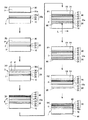
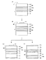
図1を参照して、本発明のある実施形態である半導体デバイスの製造方法は、Ga含有透明支持基板10上に光熱変換層21を含む中間層20aを形成して積層支持基板1を作製する工程を備える(図1(A))。また、積層支持基板1の中間層20aにGaN基板30を貼り合わせて積層貼り合わせ基板2を作製する工程を備える(図1(B))。積層貼り合わせ基板2のGaN基板30を、中間層20との貼り合わせ面から所定の深さの面Pにおいて分離することにより、積層支持基板1の中間層20上にGaN層30aが形成されたエピ成長用積層支持基板3を作製する工程を備える(図1(C))。また、エピ成長用積層支持基板3のGaN層30a上に少なくとも1層の透明半導体層40をエピタキシャル成長させることにより、デバイス用積層支持基板4を作製する工程を備える(図1(D))。また、デバイス用積層支持基板4に、Ga含有透明支持基板10およびGaN層30aおよび透明半導体層40のバンドギャップエネルギーのなかで最も低いバンドギャップエネルギーに対応する波長よりも長い波長でかつ光熱変換層が吸収しうる波長の光Lを照射して、Ga含有透明支持基板10と中間層20とを分離することにより、透明半導体層40とGaN層30aと中間層20とを含むデバイス用積層ウエハ5を作製する工程を備える(図1(E)および(F))。また、デバイス用積層ウエハ5から中間層を除去して透明半導体層40とGaN層30aとを含む透明半導体層積層ウエハ6を含む半導体デバイス7を作製する工程を備える(図1(G)および(H))。これらの工程を備えることにより、GaN層30aおよび透明半導体層40にダメージを与えることなく透明半導体層積層ウエハ6を形成することができるため、良質の半導体層を有する高品質の半導体デバイスが得られる。
[Embodiment 1]
With reference to FIG. 1, the manufacturing method of the semiconductor device which is one embodiment of this invention forms the intermediate | middle layer 20a containing the photothermal conversion layer 21 on the Ga containing transparent support substrate 10, and produces the laminated support substrate 1. FIG. A process is provided (FIG. 1 (A)). In addition, the method includes a step of manufacturing the laminated substrate 2 by attaching the GaN substrate 30 to the intermediate layer 20a of the laminated support substrate 1 (FIG. 1B). The GaN layer 30a was formed on the intermediate layer 20 of the laminated support substrate 1 by separating the GaN substrate 30 of the laminated substrate 2 on the plane P having a predetermined depth from the bonding surface with the intermediate layer 20. A step of producing a laminated support substrate 3 for epi growth is provided (FIG. 1C). In addition, the device includes a step of fabricating the device multilayer support substrate 4 by epitaxially growing at least one transparent semiconductor layer 40 on the GaN layer 30a of the epitaxial growth support substrate 3 (FIG. 1D). Further, the laminated support substrate 4 for devices has a wavelength longer than the wavelength corresponding to the lowest band gap energy among the band gap energies of the Ga-containing transparent support substrate 10, the GaN layer 30a, and the transparent semiconductor layer 40, and a photothermal conversion layer. By irradiating light L having a wavelength that can be absorbed by the Ga-containing transparent support substrate 10 and the intermediate layer 20, the device laminated wafer 5 including the transparent semiconductor layer 40, the GaN layer 30 a, and the intermediate layer 20 is separated. Is provided (FIGS. 1E and 1F). In addition, the method includes a step of fabricating a semiconductor device 7 including a transparent semiconductor layer laminated wafer 6 including a transparent semiconductor layer 40 and a GaN layer 30a by removing the intermediate layer from the device laminated wafer 5 (FIG. 1 (G) and ( H)). By providing these steps, the transparent semiconductor layer laminated wafer 6 can be formed without damaging the GaN layer 30a and the transparent semiconductor layer 40, so that a high-quality semiconductor device having a high-quality semiconductor layer can be obtained. .

(積層支持基板の作製工程)
図1(A)を参照して、積層支持基板1の作製工程は、Ga含有透明支持基板10上に光熱変換層21を含む中間層20aを形成することにより行われる。本工程により得られる積層支持基板1は、後述するように、本基板に照射される光が光熱変換層21に吸収されることにより、光熱変換層21を含む中間層20aは熱が蓄えられて高温となり、この熱によりGa含有透明支持基板10の中間層20aに接する面が分解されて、中間層20aとGa含有透明支持基板10とに分離することができる。
(Lamination support substrate manufacturing process)
With reference to FIG. 1 (A), the manufacturing process of the lamination | stacking support substrate 1 is performed by forming the intermediate | middle layer 20a containing the photothermal conversion layer 21 on the Ga containing transparent support substrate 10. FIG. As will be described later, in the laminated support substrate 1 obtained by this step, heat is stored in the intermediate layer 20a including the light-to-heat conversion layer 21 by the light irradiated to the substrate being absorbed by the light-to-heat conversion layer 21. The surface that contacts the intermediate layer 20a of the Ga-containing transparent support substrate 10 is decomposed by this heat, and the intermediate layer 20a and the Ga-containing transparent support substrate 10 can be separated.

Ga含有透明支持基板10上に中間層20aを形成する方法は、特に制限はなく、プラズマCVD(化学気相堆積)法、スパッタ法、真空蒸着法などが用いられる。   The method for forming the intermediate layer 20a on the Ga-containing transparent support substrate 10 is not particularly limited, and a plasma CVD (chemical vapor deposition) method, a sputtering method, a vacuum evaporation method, or the like is used.

光熱変換層21を含む中間層20aは、上記のように高温となる。また、透明半導体層40をエピタキシャル成長させる際に、800℃以上、場合によっては1100℃付近の高温に曝される。これらの理由から、光熱変換層21を含む中間層20aは高い耐熱性を有することが好ましく、たとえば1200℃以上の融点を有することが好ましい。また、中間層20aは、後述するように、光熱変換層21の片側または両側に透明層(たとえば、図1(A)において、第1の透明層23aおよび第2の透明層25)をさらに含むことができる。たとえば、中間層20aは、Ga含有透明支持基板10側から順に、第2の透明層25、光熱変換層21、および第1の透明層23aを含む。なお、第1の透明層23aは、後工程(図1(B))においてGaN基板30と貼り合わされて、第1の透明層23としてGaN基板30と光熱変換層21との間に位置することになる。かかる透明層(たとえば、第1の透明層23および第2の透明層25)は、後述するように、波長500nm以上600nm未満の光に対する光吸収係数が1×103cm-1以上未満であることが好ましく、たとえば、二酸化シリコン層、窒化シリコン層および酸窒化シリコン層のいずれかであることが好ましい。光熱変換層21は、後述するように、波長500nm以上600nm未満の光に対する光吸収係数が1×103cm-1以上であることが好ましく、たとえば、アモルファスシリコン層、または、モリブデン、タングステン、タンタル、チタン、白金、パラジウム、炭素、およびこれらのケイ化物、およびこれらの窒化物からなる群から選ばれる少なくとも1つを含む層であることが好ましい。 The intermediate layer 20a including the photothermal conversion layer 21 is at a high temperature as described above. Further, when the transparent semiconductor layer 40 is epitaxially grown, it is exposed to a high temperature of 800 ° C. or higher, and in some cases, near 1100 ° C. For these reasons, the intermediate layer 20a including the photothermal conversion layer 21 preferably has high heat resistance, and preferably has a melting point of, for example, 1200 ° C. or higher. Further, as will be described later, the intermediate layer 20a further includes a transparent layer (for example, the first transparent layer 23a and the second transparent layer 25 in FIG. 1A) on one side or both sides of the photothermal conversion layer 21. be able to. For example, the intermediate layer 20a includes a second transparent layer 25, a photothermal conversion layer 21, and a first transparent layer 23a in this order from the Ga-containing transparent support substrate 10 side. The first transparent layer 23a is bonded to the GaN substrate 30 in a later step (FIG. 1B) and is positioned between the GaN substrate 30 and the photothermal conversion layer 21 as the first transparent layer 23. become. Such transparent layers (for example, the first transparent layer 23 and the second transparent layer 25) have a light absorption coefficient of 1 × 10 3 cm −1 or more for light having a wavelength of 500 nm or more and less than 600 nm, as will be described later. For example, any one of a silicon dioxide layer, a silicon nitride layer, and a silicon oxynitride layer is preferable. As will be described later, the photothermal conversion layer 21 preferably has a light absorption coefficient of 1 × 10 3 cm −1 or more for light having a wavelength of 500 nm or more and less than 600 nm. For example, an amorphous silicon layer, molybdenum, tungsten, or tantalum. And a layer containing at least one selected from the group consisting of titanium, platinum, palladium, carbon, silicides thereof, and nitrides thereof.

Ga含有透明支持基板10は、後述するように、波長500nm以上600nm未満の光に対する光吸収係数が1×103cm-1以上未満であることが好ましく、たとえば、GaN支持基板であることが好ましい。 As will be described later, the Ga-containing transparent support substrate 10 preferably has a light absorption coefficient for light having a wavelength of 500 nm or more and less than 600 nm of less than 1 × 10 3 cm −1 or more, for example, a GaN support substrate. .

(積層貼り合わせ基板の作製工程)
図1(B)を参照して、積層貼り合わせ基板2の作製工程は、積層支持基板1の中間層20aにGaN基板30を貼り合わせることにより行われる。ここで、積層支持基板1の中間層20aにGaN基板30を貼り合わせる方法には、特に制限はなく、貼り合わせる面の表面を洗浄して直接貼り合わせ、その後700℃〜1000℃に昇温して接合する直接接合法、金属膜を形成し、接触させつつ昇温することで金属膜の金属を合金化させることにより接合する合金接合法、プラズマやイオンなどで貼り合わせ面を活性化させ接合する表面活性化法、などが好ましく用いられる。
(Manufacturing process of laminated substrate)
With reference to FIG. 1B, the manufacturing process of the laminated laminated substrate 2 is performed by bonding a GaN substrate 30 to the intermediate layer 20 a of the laminated supporting substrate 1. Here, the method of bonding the GaN substrate 30 to the intermediate layer 20a of the laminated support substrate 1 is not particularly limited, and the surfaces of the bonding surfaces are cleaned and bonded directly, and then heated to 700 ° C to 1000 ° C. Direct bonding method that joins together, metal film is formed, alloy bonding method that joins the metal of the metal film by alloying by raising the temperature while making contact, activated the bonding surface with plasma or ions, etc. The surface activation method is preferably used.

また、GaN基板30の貼り合わせ面には、光Lの照射時に光熱変換層からGaN基板30に伝わる熱を低減するとともに接合強度を高める観点から、積層支持基板1の中間層20aの最外層と化学的に同じ材質の層が形成されていることが好ましい。たとえば、積層支持基板1の中間層20aの最外層が第1の透明層23aである場合には、かかる第1の透明層23aと化学的に同一の材質の層である第1の透明層23bがGaN基板30の貼り合わせ面に形成されていることが好ましい。GaN基板30の第1の透明層23bを、積層支持基板1の中間層20aの第1の透明層23aに貼り合わせることにより、光熱変換層21とGaN基板30との間に第1の透明層23が形成される。こうして、光熱変換層21と、光熱変換層21とGaN基板30との間に配置される第1の透明層23と、光熱変換層21とGa含有透明支持基板10との間に配置される第2の透明層25と、を含む中間層20が形成される。   In addition, the bonded surface of the GaN substrate 30 is formed with an outermost layer of the intermediate layer 20a of the laminated support substrate 1 from the viewpoint of reducing heat transmitted from the photothermal conversion layer to the GaN substrate 30 when the light L is irradiated and increasing bonding strength. It is preferable that layers of the same material are formed chemically. For example, when the outermost layer of the intermediate layer 20a of the laminated support substrate 1 is the first transparent layer 23a, the first transparent layer 23b that is a layer of the same material as the first transparent layer 23a is used. Is preferably formed on the bonding surface of the GaN substrate 30. The first transparent layer 23 b of the GaN substrate 30 is bonded to the first transparent layer 23 a of the intermediate layer 20 a of the laminated support substrate 1, so that the first transparent layer is interposed between the photothermal conversion layer 21 and the GaN substrate 30. 23 is formed. Thus, the photothermal conversion layer 21, the first transparent layer 23 arranged between the photothermal conversion layer 21 and the GaN substrate 30, and the first transparent layer 23 arranged between the photothermal conversion layer 21 and the Ga-containing transparent support substrate 10. An intermediate layer 20 including two transparent layers 25 is formed.

(エピ成長用積層支持基板の作製工程)
図1(C)を参照して、エピ成長用積層支持基板3の作製工程は、積層貼り合わせ基板2のGaN基板30を、中間層20との貼り合わせ面から所定の深さの面Pにおいて分離することにより行われる。かかる工程により、積層支持基板1の中間層20上にGaN層30aが形成されたエピ成長用積層支持基板3が得られる。
(Manufacturing process of laminated support substrate for epi growth)
Referring to FIG. 1C, in the process of manufacturing the epitaxial growth laminated support substrate 3, the GaN substrate 30 of the laminated laminated substrate 2 is placed on the surface P having a predetermined depth from the bonded surface with the intermediate layer 20. This is done by separating. Through this step, the epitaxial growth laminated support substrate 3 in which the GaN layer 30a is formed on the intermediate layer 20 of the laminated support substrate 1 is obtained.

GaN基板30を中間層20との貼り合わせ面から所定の深さの面Pにおいて分離する方法には、特に制限はなく、GaN基板30を上記の面Pにおいて切断する方法や、積層支持基板1に脆弱領域を形成させるため、積層支持基板1に貼り合わせる前に上記面Pにイオンを注入したGaN基板30を積層支持基板1に貼り合せた後、熱および/または応力を加えることにより、イオン注入により脆化された面Pにおいて分離する方法、などが用いられる。かかる方法により、積層支持基板1の中間層20上に厚さ0.05μm〜100μmのGaN層30aを形成することができる。   The method for separating the GaN substrate 30 from the bonding surface with the intermediate layer 20 on the surface P having a predetermined depth is not particularly limited, and a method for cutting the GaN substrate 30 on the surface P, the laminated support substrate 1 or the like. In order to form a fragile region, the GaN substrate 30 into which ions have been implanted into the surface P before being bonded to the laminated support substrate 1 is bonded to the stacked support substrate 1, and then heat and / or stress is applied to the ions. A method of separating on the surface P embrittled by implantation is used. By such a method, the GaN layer 30a having a thickness of 0.05 μm to 100 μm can be formed on the intermediate layer 20 of the laminated support substrate 1.

ここで、Ga含有透明支持基板10は、エピタキシャル成長やアニール処理時においてGaN層30aにクラックなどを発生させない観点から、その熱膨張係数がGaN層30aの熱膨張係数と同一または近似していることが好ましく、GaN層30aの主表面の面方位と同一の面方位の主表面を有するGaN支持基板であることが特に好ましい。   Here, the Ga-containing transparent support substrate 10 has a thermal expansion coefficient that is the same as or close to the thermal expansion coefficient of the GaN layer 30a from the viewpoint of not generating cracks in the GaN layer 30a during epitaxial growth or annealing. A GaN support substrate having a main surface having the same plane orientation as that of the main surface of the GaN layer 30a is particularly preferable.

(デバイス用積層支持基板の作製工程)
図1(D)を参照して、デバイス用積層支持基板4の作製工程は、エピ成長用積層支持基板3のGaN層30a上に少なくとも1層の透明半導体層40をエピタキシャル成長させることにより行われる。
(Manufacturing process of laminated support substrate for devices)
Referring to FIG. 1D, the process for manufacturing the device multilayer support substrate 4 is performed by epitaxially growing at least one transparent semiconductor layer 40 on the GaN layer 30 a of the epitaxial growth support substrate 3.

ここで、熱膨張係数がGaN層30aの熱膨張係数と同一または近似するGaN含有透明支持基板10を用いることにより、エピタキシャル成長やアニール処理時においてクラックなどを発生させることなく、品質のよい少なくとも1層の透明半導体層40を形成することができる。かかる観点から、Ga含有透明支持基板10は、たとえばGaN層30aの主表面の面方位と同一の面方位の主表面を有するGaN支持基板であることが好ましい。   Here, by using the GaN-containing transparent support substrate 10 whose thermal expansion coefficient is the same as or close to the thermal expansion coefficient of the GaN layer 30a, at least one layer having high quality without causing cracks during epitaxial growth or annealing treatment. The transparent semiconductor layer 40 can be formed. From this point of view, the Ga-containing transparent support substrate 10 is preferably a GaN support substrate having a main surface with the same plane orientation as that of the main surface of the GaN layer 30a, for example.

エピ成長用積層支持基板3のGaN層30a上に少なくとも1層の透明半導体層40をエピタキシャル成長させる方法には、特に制限はないが、品質のよい透明半導体層を成長させる観点から、MOCVD(有機金属化学気相堆積)法、MBE(分子線エピタキシ)法、HVPE(ハイドライド気相成長)法などの気相法などが好ましく用いられる。   The method for epitaxially growing at least one transparent semiconductor layer 40 on the GaN layer 30a of the epitaxial growth laminated support substrate 3 is not particularly limited, but from the viewpoint of growing a high-quality transparent semiconductor layer, MOCVD (organometallic) A vapor phase method such as a chemical vapor deposition method, an MBE (molecular beam epitaxy) method or an HVPE (hydride vapor phase epitaxy) method is preferably used.

エピ成長用積層支持基板3上にエピタキシャル成長させる少なくとも1層の透明半導体層40は、クラックなどを発生させることなく品質のよい透明半導体層40を成長させる観点から、GaN層30aと格子定数が同一または近似しており、また、GaN層30aおよびGa含有透明支持基板10と熱膨張係数が同一または近似していることが好ましい。また、透明半導体層40は、後述のように、波長500nm以上600nm未満の光に対する光吸収係数が1×103cm-1未満であることが好ましい。また、中間層を透過した照射光を吸収しないという観点から、透明半導体層40は、デバイス用積層支持基板4に照射される光よりも短波長でかつ波長300nm以上550nm以下のピーク波長を有する光を放出する発光層45を含むことが好ましい。これらの観点から、透明半導体層40は、たとえば、III族窒化物半導体層であることが好ましい。 At least one transparent semiconductor layer 40 epitaxially grown on the epitaxial growth laminated support substrate 3 has the same lattice constant as that of the GaN layer 30a from the viewpoint of growing a high-quality transparent semiconductor layer 40 without generating cracks or the like. It is preferable that the thermal expansion coefficients are the same as or similar to those of the GaN layer 30a and the Ga-containing transparent support substrate 10. The transparent semiconductor layer 40 preferably has a light absorption coefficient of less than 1 × 10 3 cm −1 for light having a wavelength of 500 nm or more and less than 600 nm, as will be described later. Further, from the viewpoint of not absorbing the irradiation light transmitted through the intermediate layer, the transparent semiconductor layer 40 is light having a shorter wavelength than the light irradiated to the laminated support substrate 4 for devices and a peak wavelength of not less than 300 nm and not more than 550 nm. It is preferable to include a light emitting layer 45 that emits. From these viewpoints, the transparent semiconductor layer 40 is preferably a group III nitride semiconductor layer, for example.

(デバイス用積層ウエハの作製工程)
図1(E)および(F)を参照して、デバイス用積層ウエハ5の作製工程は、デバイス用積層支持基板4に、Ga含有透明支持基板10およびGaN層30aおよび透明半導体層40のバンドギャップエネルギーのなかで最も低いバンドギャップエネルギーに対応する波長よりも長い波長でかつ光熱変換層が吸収しうる波長の光Lを照射して、Ga含有透明支持基板10と中間層20とを分離することにより行われる。かかる工程により、透明半導体層40とGaN層30aと中間層20とを含むデバイス用積層ウエハ5が得られる。ここで、図1(E)には、デバイス用積層支持基板4のGa含有透明支持基板10側から光Lが照射される場合が記載されているが、デバイス用積層支持基板4の透明半導体層40側から光Lが照射されてもよい。
(Process for producing laminated wafers for devices)
Referring to FIGS. 1E and 1F, the device laminated wafer 5 is manufactured in such a manner that the device laminated support substrate 4 has a band gap between the Ga-containing transparent support substrate 10, the GaN layer 30a, and the transparent semiconductor layer 40. Irradiating light L having a wavelength longer than the wavelength corresponding to the lowest bandgap energy among the energies and capable of being absorbed by the photothermal conversion layer, thereby separating the Ga-containing transparent support substrate 10 and the intermediate layer 20 from each other. Is done. Through this process, the device laminated wafer 5 including the transparent semiconductor layer 40, the GaN layer 30a, and the intermediate layer 20 is obtained. Here, FIG. 1 (E) shows a case where light L is irradiated from the Ga-containing transparent support substrate 10 side of the device multilayer support substrate 4, but the transparent semiconductor layer of the device multilayer support substrate 4. The light L may be irradiated from the 40 side.

本工程において、デバイス用積層支持基板4に照射される光の光子1個あたりのエネルギーは、Ga含有透明支持基板10、GaN層30aおよび透明半導体層40のバンドギャップエネルギーのなかで最も低いバンドギャップエネルギーよりも低いため、Ga含有透明支持基板10、GaN層30aおよび透明半導体層40では光が吸収されずに透過する。これにより、Ga含有透明支持基板10、GaN層30aおよび透明半導体層40では不要な光吸収に伴い発生する熱を起因とするダメージを回避できる。   In this step, the energy per photon of light irradiated on the device multilayer support substrate 4 is the lowest band gap energy among the band gap energies of the Ga-containing transparent support substrate 10, the GaN layer 30a, and the transparent semiconductor layer 40. Since it is lower than energy, light is not absorbed by the Ga-containing transparent support substrate 10, the GaN layer 30a, and the transparent semiconductor layer 40, but is transmitted. Thereby, in the Ga containing transparent support substrate 10, the GaN layer 30a, and the transparent semiconductor layer 40, damage caused by heat generated due to unnecessary light absorption can be avoided.

デバイス用積層支持基板4に照射された光は、光熱変換層21で吸収され熱に変換される。この熱により、Ga含有透明支持基板10の中間層20に接する面が分解されて、デバイス用積層支持基板4はGa含有透明支持基板10と中間層20との間で分離される。こうして、透明半導体層40とGaN層30aと中間層20とを含むデバイス用積層ウエハ5が得られる。   The light irradiated to the device multilayer support substrate 4 is absorbed by the photothermal conversion layer 21 and converted into heat. With this heat, the surface of the Ga-containing transparent support substrate 10 that contacts the intermediate layer 20 is decomposed, and the laminated support substrate 4 for devices is separated between the Ga-containing transparent support substrate 10 and the intermediate layer 20. Thus, the device laminated wafer 5 including the transparent semiconductor layer 40, the GaN layer 30a, and the intermediate layer 20 is obtained.

デバイス用積層支持基板4に照射される光は、その波長がGa含有透明支持基板10、GaN層30aおよび透明半導体層40のバンドギャップエネルギーのなかで最も低いバンドギャップエネルギーに対応する波長よりも長ければ特に制限はないが、比較的低い投入エネルギーで効率よくGa含有透明支持基板10と中間層20とを分離するためには、波長500nm以上600nm未満のレーザ光であることが好ましく、たとえば波長808nmの半導体レーザで励起された波長1064nmのNd:YAGレーザ光(ここで、Nd:YAGとは、Nd(ネオジム)を添加したY(イットリウム)・A(アルミニウム)・G(ガーネット)により形成される結晶をいう)またはNd:YVO4レーザ光(ここで、Nd:YVO4とは、Nd(ネオジム)を添加したY(イットリウム)・V(バナジウム)・O4(オキサイド)またはY(イットリウム)・VO4(バナデート))により形成される結晶をいう)をLiB35のなどのいわゆるSHG(Second Harmonic Generation;第2高調波)結晶で変換した波長532nmのレーザ光が好ましく用いられる。この波長の光は、Ga含有透明支持基板10、GaN層30aおよび透明半導体層40を構成し得る、たとえば、GaN、InGaN、AlGaNなどのIII族窒化物や、第1および第2の透明層23、25を構成し得るたとえば二酸化シリコン、窒化シリコンおよび酸窒化シリコンのいずれかには吸収されないが、光熱変換層21を構成し得るたとえばアモルファスシリコンには好適に吸収される。 The light irradiated to the device multilayer support substrate 4 has a wavelength longer than the wavelength corresponding to the lowest band gap energy among the band gap energies of the Ga-containing transparent support substrate 10, the GaN layer 30a, and the transparent semiconductor layer 40. Although there is no particular limitation, in order to efficiently separate the Ga-containing transparent support substrate 10 and the intermediate layer 20 with relatively low input energy, laser light with a wavelength of 500 nm or more and less than 600 nm is preferable, for example, a wavelength of 808 nm. Nd: YAG laser light having a wavelength of 1064 nm excited by the semiconductor laser (where Nd: YAG is formed of Y (yttrium), A (aluminum), G (garnet) added with Nd (neodymium) Crystal)) or Nd: YVO 4 laser light (where Nd: YVO 4 is Nd (Neodymium) added Y (yttrium) · V (vanadium) · O 4 (oxide) or Y (yttrium) · VO 4 (vanadate)))) is called so-called LiB 3 O 5 A laser beam having a wavelength of 532 nm converted by an SHG (Second Harmonic Generation) crystal is preferably used. The light having this wavelength can constitute the Ga-containing transparent support substrate 10, the GaN layer 30 a and the transparent semiconductor layer 40, for example, a group III nitride such as GaN, InGaN, AlGaN, or the first and second transparent layers 23. 25 can be absorbed by any one of silicon dioxide, silicon nitride, and silicon oxynitride, but is preferably absorbed by, for example, amorphous silicon that can form the photothermal conversion layer 21.

ここで、Ga含有透明支持基板10としてGaN支持基板を用いる場合は、上記光Lの照射により、GaN支持基板において中間層に接する面が金属Gaと窒素(N2)ガスに分解され、GaN支持基板と中間層との間に金属Gaが析出する。金属Gaは29.8℃で融解するため、この温度以上に加熱されることにより、GaN支持基板と中間層とが分離される。 Here, when a GaN support substrate is used as the Ga-containing transparent support substrate 10, the surface in contact with the intermediate layer in the GaN support substrate is decomposed into metal Ga and nitrogen (N 2 ) gas by irradiation with the light L, and the GaN support is supported. Metal Ga is deposited between the substrate and the intermediate layer. Since metallic Ga melts at 29.8 ° C., the GaN support substrate and the intermediate layer are separated by heating to a temperature higher than this temperature.

デバイス用積層支持基板4においては、GaN層30a上に品質のよい透明半導体層40を形成させる観点から、Ga含有透明支持基板10はGaN支持基板であり、透明半導体層40はIII族窒化物半導体層であることが好ましい。かかる場合においては、GaN層30a、GaN支持基板(Ga含有透明支持基板10)およびIII族窒化物半導体層(透明半導体層40)は、通常波長500nm以上600nm未満の光に対する光吸収係数が1×103cm-1未満である。したがって、GaN支持基板と中間層との分離のために、デバイス用積層支持基板4に照射される光は、GaN層30a、GaN支持基板(Ga含有透明支持基板10)およびIII族窒化物半導体層(透明半導体層40)に与えるダメージを低減する観点から、波長500nm以上600nm未満のレーザ光であることが好ましい。 In the laminated support substrate 4 for devices, from the viewpoint of forming a high-quality transparent semiconductor layer 40 on the GaN layer 30a, the Ga-containing transparent support substrate 10 is a GaN support substrate, and the transparent semiconductor layer 40 is a group III nitride semiconductor. A layer is preferred. In such a case, the GaN layer 30a, the GaN support substrate (Ga-containing transparent support substrate 10), and the group III nitride semiconductor layer (transparent semiconductor layer 40) usually have a light absorption coefficient of 1 × for light with a wavelength of 500 nm or more and less than 600 nm. Less than 10 3 cm −1 . Therefore, for the separation of the GaN support substrate and the intermediate layer, the light irradiated to the laminated support substrate 4 for devices is the GaN layer 30a, the GaN support substrate (Ga-containing transparent support substrate 10), and the group III nitride semiconductor layer. From the viewpoint of reducing damage to the (transparent semiconductor layer 40), it is preferably a laser beam having a wavelength of 500 nm or more and less than 600 nm.

中間層20は、Ga含有透明支持基板10と中間層20との間の分離に際して高温となる。また、透明半導体層40をエピタキシャル成長させる際に、800℃以上、場合によっては1100℃付近の高温に曝される。これらの理由から、中間層20は高い耐熱性を有することが好ましく、たとえば1200℃以上の融点を有することが好ましい。すなわち、光熱変換層21は、高い耐熱性を有していることが好ましく、たとえば1200℃以上の融点を有することが好ましい。また、デバイス用積層支持基板4に照射される光が波長500nm以上600nm未満のレーザ光である場合は、光熱変換層21は、その波長域の光を効率よく吸収することが好ましいため、波長500nm以上600nm未満の光に対する光吸収係数が1×103cm-1以上であることが好ましい。以上の要件を満たす材料からなる層として、光熱変換層21は、たとえばアモルファスシリコン層であることが好ましい。 The intermediate layer 20 becomes a high temperature during the separation between the Ga-containing transparent support substrate 10 and the intermediate layer 20. Further, when the transparent semiconductor layer 40 is epitaxially grown, it is exposed to a high temperature of 800 ° C. or higher, and in some cases, near 1100 ° C. For these reasons, the intermediate layer 20 preferably has high heat resistance, for example, preferably has a melting point of 1200 ° C. or higher. That is, the photothermal conversion layer 21 preferably has high heat resistance, and preferably has a melting point of 1200 ° C. or higher, for example. Moreover, when the light irradiated to the laminated support substrate 4 for devices is a laser beam having a wavelength of 500 nm or more and less than 600 nm, the photothermal conversion layer 21 preferably absorbs light in the wavelength region efficiently, so that the wavelength of 500 nm. The light absorption coefficient for light of less than 600 nm is preferably 1 × 10 3 cm −1 or more. As a layer made of a material that satisfies the above requirements, the photothermal conversion layer 21 is preferably, for example, an amorphous silicon layer.

デバイス用積層支持基板4において、光熱変換層21を含む中間層20は、Ga含有透明支持基板10およびGaN層30aに接している。このため、上記の光Lの照射により、光熱変換層21が加熱されて高温になると、その熱がGa含有透明支持基板10だけでなく、GaN層30aおよびGaN層30aに接している透明半導体層40にも伝わり、GaN層30aおよび透明半導体層40にもダメージを与えるおそれがある。このようなGaN層30aおよび透明半導体層40に与えるダメージを低減し、また中間層20とGaN層30aとの接合は保持しつつ中間層20とGa含有透明支持基板10との間で確実に分離するため、中間層20は、中間層20の光熱変換層21とGaN層30aとの間に配置される第1の透明層23をさらに含むことが好ましい。また、第1の透明層23は、光熱変換層21中の原子(たとえばアモルファスシリコン層中のSi原子)のマイグレーションによるGaN層30aおよび透明半導体層40への原子拡散および、光照射時のGaN層30aおよび透明半導体層40へ与えられるダメージを低減するとともに中間層20とGaN層30aとの接合強度も高める。   In the device multilayer support substrate 4, the intermediate layer 20 including the photothermal conversion layer 21 is in contact with the Ga-containing transparent support substrate 10 and the GaN layer 30 a. For this reason, when the photothermal conversion layer 21 is heated to a high temperature by irradiation with the light L described above, the heat is in contact with not only the Ga-containing transparent support substrate 10 but also the GaN layer 30a and the GaN layer 30a. 40 and may damage the GaN layer 30a and the transparent semiconductor layer 40. Such damage to the GaN layer 30a and the transparent semiconductor layer 40 is reduced, and the intermediate layer 20 and the Ga-containing transparent support substrate 10 are reliably separated while maintaining the bonding between the intermediate layer 20 and the GaN layer 30a. Therefore, it is preferable that the intermediate layer 20 further includes a first transparent layer 23 disposed between the photothermal conversion layer 21 of the intermediate layer 20 and the GaN layer 30a. Further, the first transparent layer 23 is formed by diffusing atoms into the GaN layer 30a and the transparent semiconductor layer 40 due to migration of atoms in the photothermal conversion layer 21 (for example, Si atoms in the amorphous silicon layer), and a GaN layer during light irradiation. The damage given to 30a and the transparent semiconductor layer 40 is reduced and the bonding strength between the intermediate layer 20 and the GaN layer 30a is also increased.

かかる第1の透明層23は、特に制限はないが、不要な光吸収に伴う発熱によるGaN層30aおよび透明半導体層40への熱ダメージおよび/または熱に伴う膨張による応力ダメージを生じさせないために、Ga含有透明支持基板10、GaN層30aおよび透明半導体層40と同様の透明性、すなわち波長500nm以上600nm以下の光に対する光吸収係数が1×103cm-1未満であることが好ましい。また、第1の透明層23は、上記のように高温となる光熱変換層21に接する。また、透明半導体層40をエピタキシャル成長させる際に、800℃以上、場合によっては1100℃付近の高温に曝される。これらの理由から、第1の透明層23は高い耐熱性を有することが好ましく、たとえば1200℃以上の融点を有することが好ましい。上記の要件を満たす材料として 、第1の透明層は、たとえば、二酸化シリコン層、窒化シリコン層および酸窒化シリコン層のいずれかであることが特に好ましい。 The first transparent layer 23 is not particularly limited, in order not to cause thermal damage to the GaN layer 30a and the transparent semiconductor layer 40 due to heat generation accompanying unnecessary light absorption and / or stress damage due to expansion due to heat. The transparency similar to that of the Ga-containing transparent support substrate 10, the GaN layer 30a, and the transparent semiconductor layer 40, that is, the light absorption coefficient for light having a wavelength of 500 nm to 600 nm is preferably less than 1 × 10 3 cm −1 . Further, the first transparent layer 23 is in contact with the photothermal conversion layer 21 that is at a high temperature as described above. Further, when the transparent semiconductor layer 40 is epitaxially grown, it is exposed to a high temperature of 800 ° C. or higher, and in some cases, near 1100 ° C. For these reasons, the first transparent layer 23 preferably has high heat resistance, for example, preferably has a melting point of 1200 ° C. or higher. As a material that satisfies the above requirements, the first transparent layer is particularly preferably, for example, any one of a silicon dioxide layer, a silicon nitride layer, and a silicon oxynitride layer.

また、光熱変換層21中の原子(たとえばアモルファスシリコン層中のSi原子)のマイグレーションによる原子拡散を抑制するとともに中間層20とGa含有透明支持基板10との接合強度を高める観点から、中間層20は、中間層20の光熱変換層21とGa含有透明支持基板10との間に配置される第2の透明層25をさらに含むことが好ましい。   Further, from the viewpoint of suppressing atomic diffusion due to migration of atoms in the photothermal conversion layer 21 (for example, Si atoms in the amorphous silicon layer) and increasing the bonding strength between the intermediate layer 20 and the Ga-containing transparent support substrate 10, the intermediate layer 20. Preferably further includes a second transparent layer 25 disposed between the photothermal conversion layer 21 of the intermediate layer 20 and the Ga-containing transparent support substrate 10.

かかる第2の透明層25は、特に制限はないが、不要な光吸収に伴う発熱によるGaN層30aおよび透明半導体層40への熱ダメージおよび/または熱に伴う膨張による応力ダメージを生じさせないために、Ga含有透明支持基板10、GaN層30aおよび透明半導体層40と同様の透明性、すなわち波長500nm以上600nm以下の光に対する光吸収係数が1×103cm-1未満であることが好ましい。また、第2の透明層25は、上記のように高温となる光熱変換層21に接する。また、透明半導体層40をエピタキシャル成長させる際に、800℃以上、場合によっては1100℃付近の高温に曝される。これらの理由から、第2の透明層25は高い耐熱性を有することが好ましく、たとえば1200℃以上の融点を有することが好ましい。上記の要件を満たす材料として 、第2の透明層は、たとえば、二酸化シリコン層、窒化シリコン層および酸窒化シリコン層のいずれかであることが特に好ましい。 The second transparent layer 25 is not particularly limited, but it does not cause thermal damage to the GaN layer 30a and the transparent semiconductor layer 40 due to heat generation accompanying unnecessary light absorption and / or stress damage due to expansion due to heat. The transparency similar to that of the Ga-containing transparent support substrate 10, the GaN layer 30a, and the transparent semiconductor layer 40, that is, the light absorption coefficient for light having a wavelength of 500 nm to 600 nm is preferably less than 1 × 10 3 cm −1 . Further, the second transparent layer 25 is in contact with the photothermal conversion layer 21 that is at a high temperature as described above. Further, when the transparent semiconductor layer 40 is epitaxially grown, it is exposed to a high temperature of 800 ° C. or higher, and in some cases, near 1100 ° C. For these reasons, the second transparent layer 25 preferably has high heat resistance, for example, preferably has a melting point of 1200 ° C. or higher. As a material that satisfies the above requirements, the second transparent layer is particularly preferably, for example, any one of a silicon dioxide layer, a silicon nitride layer, and a silicon oxynitride layer.

第1の透明層23および第2の透明層25の両方が存在する場合、第1の透明層23の厚さは第2の透明層25の厚さに比べて大きいことが好ましい。これにより、中間層20とGa含有Ga含有透明支持基板10との貼り合わせ面の温度を、中間層20とGaN層30aとの貼り合わせ面の温度より高くできる。これを利用して、中間層20とGa含有透明支持基板10との貼り合わせ面の温度を金属Gaが形成可能な温度以上に、中間層20とGaN層30aとの貼り合わせ面の温度を金属Gaが形成可能な温度未満にすることで、中間層20とGaN層30aの貼り合わせ面には金属Gaを形成させずに、中間層20とGa含有透明支持基板10との貼り合わせ面にのみ金属Ga60を形成することができる。これにより、デバイス用積層ウエハ5を、デバイス用積層支持基板4の中間層20とGa含有透明支持基板10との貼り合わせ面の選択分離により、形成できるようになる。   When both the first transparent layer 23 and the second transparent layer 25 are present, the thickness of the first transparent layer 23 is preferably larger than the thickness of the second transparent layer 25. Thereby, the temperature of the bonding surface of the intermediate layer 20 and the Ga-containing Ga-containing transparent support substrate 10 can be made higher than the temperature of the bonding surface of the intermediate layer 20 and the GaN layer 30a. By utilizing this, the temperature of the bonding surface between the intermediate layer 20 and the Ga-containing transparent support substrate 10 is set to be higher than the temperature at which the metal Ga can be formed, and the temperature of the bonding surface between the intermediate layer 20 and the GaN layer 30a is set to the metal. By making the temperature lower than the temperature at which Ga can be formed, metal Ga is not formed on the bonding surface of the intermediate layer 20 and the GaN layer 30a, but only on the bonding surface of the intermediate layer 20 and the Ga-containing transparent support substrate 10. Metal Ga60 can be formed. Thus, the device laminated wafer 5 can be formed by selective separation of the bonding surfaces of the intermediate layer 20 of the device laminated support substrate 4 and the Ga-containing transparent support substrate 10.

また、第2の透明層25の厚さは、特に制限はないが、中間層20における光熱変換層21と第2の透明層25との密着性を良好に担保するとともに、Ga含有透明支持基板10と中間層20の第2の透明層25との界面において選択的で効率のよい分離を確保する観点から、第2の透明層25の厚さを光熱変換層21の厚さの0.3倍以上2.5倍以下にすることが特に好ましい。   In addition, the thickness of the second transparent layer 25 is not particularly limited, but ensures good adhesion between the photothermal conversion layer 21 and the second transparent layer 25 in the intermediate layer 20, and a Ga-containing transparent support substrate. 10 and the second transparent layer 25 of the intermediate layer 20 from the viewpoint of ensuring selective and efficient separation, the thickness of the second transparent layer 25 is set to 0.3 of the thickness of the photothermal conversion layer 21. It is particularly preferable to set it to be not less than twice and not more than 2.5.

こうして、透明半導体層40とGaN層30aとを含むデバイス用積層ウエハ5が得られる。ここで、デバイス用積層ウエハ5は、Ga含有透明支持基板10の分離の際に、Ga含有透明支持基板10と中間層20と界面に形成される金属Ga60を中間層20の表面に有する。   In this way, the device laminated wafer 5 including the transparent semiconductor layer 40 and the GaN layer 30a is obtained. Here, the device laminated wafer 5 has, on the surface of the intermediate layer 20, a metal Ga 60 formed at the interface between the Ga-containing transparent support substrate 10 and the intermediate layer 20 when the Ga-containing transparent support substrate 10 is separated.

なお、本工程で得られるデバイス用積層ウエハ5および次工程で得られる透明半導体層積層ウエハ6(GaN層30aと透明半導体層40との積層ウエハをいう。以下同じ。)は機械強度が極めて低い。このため、得られるデバイス用積層ウエハ5および透明半導体層積層ウエハ6の機械強度を補強するため、本工程の前に、デバイス用積層支持基板4の透明半導体層積層ウエハ6の機械強度を補強するために、仮支持基材または透明半導体層積層ウエハ支持基板を貼り合わせることが好ましい。   Note that the device laminated wafer 5 obtained in this step and the transparent semiconductor layer laminated wafer 6 (referred to as a laminated wafer of the GaN layer 30a and the transparent semiconductor layer 40) obtained in the next step have extremely low mechanical strength. . For this reason, in order to reinforce the mechanical strength of the resulting device laminated wafer 5 and transparent semiconductor layer laminated wafer 6, the mechanical strength of the transparent semiconductor layer laminated wafer 6 of the device laminated support substrate 4 is reinforced before this step. Therefore, it is preferable to bond a temporary support base material or a transparent semiconductor layer laminated wafer support substrate together.

たとえば、図1(E)を参照して、デバイス用積層支持基板4の透明半導体層40の最外層に接着剤51を介在させて仮支持基材50を貼り合わせることができる。仮支持基材50は、特に制限はないが、光Lの照射時に光熱変換層21を透過した照射光を吸収して不要な熱を発生させないようにする観点から、サファイア基板などが好ましく用いられる。また、接着剤51は、特に制限はないが、光Lの照射時に光熱変換層21を透過した照射光を吸収して不要な熱を発生させたり分解されたりせず、さらに後工程で仮支持基材50をデバイス用積層ウエハ5から分離することが容易な観点から、Brewer Science社製Waferbond HT−10,10などが好ましく用いられる。   For example, referring to FIG. 1E, the temporary support base material 50 can be bonded to the outermost layer of the transparent semiconductor layer 40 of the laminated support substrate 4 for devices with an adhesive 51 interposed. Although there is no restriction | limiting in particular in the temporary support base material 50, From a viewpoint of absorbing the irradiation light which permeate | transmitted the photothermal conversion layer 21 at the time of irradiation of the light L, and generating an unnecessary heat | fever, a sapphire substrate etc. are used preferably. . The adhesive 51 is not particularly limited, but absorbs the irradiation light transmitted through the light-to-heat conversion layer 21 when irradiated with the light L, does not generate unnecessary heat, and is not decomposed. From the viewpoint of easy separation of the substrate 50 from the device laminated wafer 5, Waferbond HT-10, 10 manufactured by Brewer Science, Inc. is preferably used.

上記の仮支持基材50は、後の工程において、デバイス用積層支持基板4からGa含有透明支持基板10が分離されてデバイス用積層ウエハ5が形成され(図1(E)および(F))、次いでデバイス用積層ウエハ5から金属Ga60および中間層20が分離除去されて透明半導体層積層ウエハ6が形成され(図1(G))、次いで透明半導体層積層ウエハ6のGaN層30aに透明半導体層積層ウエハ支持基板70が貼り合わされて透明半導体層40が機械強度的に支持された後に、除去される(図1(H))。   In the temporary support base material 50 described above, the Ga-containing transparent support substrate 10 is separated from the device multilayer support substrate 4 to form the device multilayer wafer 5 in a later step (FIGS. 1E and 1F). Then, the metal Ga 60 and the intermediate layer 20 are separated and removed from the device laminated wafer 5 to form the transparent semiconductor layer laminated wafer 6 (FIG. 1G), and then the transparent semiconductor layer is formed on the GaN layer 30a of the transparent semiconductor layer laminated wafer 6. After the layer laminated wafer support substrate 70 is bonded and the transparent semiconductor layer 40 is supported mechanically, it is removed (FIG. 1 (H)).

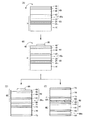
また、図4(A)を参照して、本工程の前に、上記仮支持基材に替えて、透明半導体層積層ウエハ支持基板70をデバイス用積層支持基板4の透明半導体層40に貼り合わせることができる。かかる場合には、後の工程において、透明半導体層積層ウエハ支持基板70が貼り合わされたデバイス用積層支持基板4CからGa含有透明支持基板10が分離されて支持基板付のデバイス用積層ウエハ5Cが形成され(図4(B)および(C))、次いで支持基板付のデバイス用積層ウエハ5Cから金属Ga60および中間層20が分離除去されて支持基板付の透明半導体層積層ウエハ6Cが形成され(図4(D))、次いで支持基板付の透明半導体層積層ウエハ6Cに電極などが形成されて半導体デバイス7(図4(E))が得られる。すなわち、仮支持基材に替えて、透明半導体層積層ウエハ支持基板をデバイス用積層支持基板の透明半導体層に貼り合わせる場合は、仮支持基材を貼り合わせる工程およびそれを除去する工程を必要としない。   Also, referring to FIG. 4A, before this step, instead of the temporary support substrate, the transparent semiconductor layer laminated wafer support substrate 70 is bonded to the transparent semiconductor layer 40 of the device multilayer support substrate 4. be able to. In such a case, in a subsequent process, the Ga-containing transparent support substrate 10 is separated from the device support multilayer substrate 4C to which the transparent semiconductor layer laminate wafer support substrate 70 is bonded to form a device multilayer wafer 5C with a support substrate. Then, the metal Ga 60 and the intermediate layer 20 are separated and removed from the device laminated wafer 5C with a support substrate to form a transparent semiconductor layer laminated wafer 6C with a support substrate (FIG. 4B and FIG. 4C) (FIG. 4B and FIG. 4C). 4 (D)), and then electrodes and the like are formed on the transparent semiconductor layer laminated wafer 6C with a supporting substrate to obtain the semiconductor device 7 (FIG. 4E). That is, instead of the temporary support substrate, when the transparent semiconductor layer laminated wafer support substrate is bonded to the transparent semiconductor layer of the device multilayer support substrate, a step of bonding the temporary support substrate and a step of removing it are required. do not do.

(透明半導体層積層ウエハの作製工程)
図1(G)を参照して、透明半導体層積層ウエハ6の作製工程は、デバイス用積層ウエハ5から中間層20を除去することにより行われる。かかる工程により、透明半導体層40とGaN層30aとを含む透明半導体層積層ウエハ6が得られる。デバイス用積層ウエハ5から中間層20を除去する方法は、特に制限はなく、半導体プロセスで一般的に用いられるウェットエッチング、ドライエッチングなどの方法を利用できる。
(Transparent semiconductor layer laminated wafer manufacturing process)
Referring to FIG. 1G, the manufacturing process of the transparent semiconductor layer laminated wafer 6 is performed by removing the intermediate layer 20 from the device laminated wafer 5. Through this process, the transparent semiconductor layer laminated wafer 6 including the transparent semiconductor layer 40 and the GaN layer 30a is obtained. The method for removing the intermediate layer 20 from the device laminated wafer 5 is not particularly limited, and methods such as wet etching and dry etching generally used in semiconductor processes can be used.

(半導体デバイスの作製工程)
図1(H)を参照して、半導体デバイス7の作製工程は、透明半導体層積層ウエハ6に透明半導体層積層ウエハ支持基板70を貼り合わせることにより行われる。かかる工程により、半導体デバイス7が得られる。
(Semiconductor device fabrication process)
Referring to FIG. 1H, the manufacturing process of the semiconductor device 7 is performed by bonding a transparent semiconductor layer laminated wafer support substrate 70 to the transparent semiconductor layer laminated wafer 6. Through this process, the semiconductor device 7 is obtained.

透明半導体層積層ウエハ6に透明半導体層積層ウエハ支持基板70を貼り合わせる方法には、特に制限はなく、貼り合わせる面の表面を洗浄して直接貼り合わせ、その後700℃〜1000℃に昇温して接合することによる直接接合法、プラズマやイオンなどで貼り合わせ面を活性化させ接合することによる表面活性化法などが好ましく用いられる。   The method for bonding the transparent semiconductor layer laminated wafer support substrate 70 to the transparent semiconductor layer laminated wafer 6 is not particularly limited, and the surfaces of the surfaces to be bonded are washed and directly bonded, and then heated to 700 ° C. to 1000 ° C. For example, a direct bonding method by bonding and a surface activation method by activating and bonding the bonding surface with plasma or ions are preferably used.

ここで、図2(E)〜(F)および図3(E)〜(G)を参照して、本半導体デバイス7においては、透明半導体層40が波長300nm以上550nm以下のピーク波長を有する光を放出する発光層45を含む場合は、透明半導体層積層ウエハ支持基板は、波長が300nm以上550nm以下の光に対する光吸収係数が1×104cm-1未満であることが好ましい。これにより内部吸収を低減し、光取り出し効率の高い半導体光デバイスを作製できる。かかる観点から、透明半導体層積層ウエハ支持基板70は、たとえば、サファイア、スピネル、石英、窒化アルミニウム、ダイヤモンドおよびガラスからなる群から選ばれる少なくとも1つを含むことが好ましい。 Here, with reference to FIGS. 2 (E) to 2 (F) and FIGS. 3 (E) to (G), in the present semiconductor device 7, the transparent semiconductor layer 40 has light having a peak wavelength of not less than 300 nm and not more than 550 nm. In the case where the light emitting layer 45 that emits light is included, the transparent semiconductor layer laminated wafer supporting substrate preferably has a light absorption coefficient of less than 1 × 10 4 cm −1 for light having a wavelength of 300 nm to 550 nm. As a result, it is possible to produce a semiconductor optical device with reduced internal absorption and high light extraction efficiency. From this viewpoint, the transparent semiconductor layer laminated wafer support substrate 70 preferably includes at least one selected from the group consisting of sapphire, spinel, quartz, aluminum nitride, diamond, and glass.

また、図3(E)〜(G)および図4(A)〜(E)を参照して、本半導体デバイス7においては、デバイスに積層方向の導電性を具備させる目的で、透明半導体層積層ウエハ支持基板70は、比抵抗が10Ωcm以下の導電性を有することが好ましい。デバイスに積層方向の導電性を具備させることができれば、半導体デバイス7はたとえば図3(G)に示すようにその両主表面にそれぞれp−電極80とn−電極90を形成できる。これにより、両電極を一主表面に形成しなければならない場合(たとえば、図2(F)参照)に比べて、透明半導体層40の一部を除去する必要がなくなるため、より広い面積をデバイスの動作(すなわち発光)に利用できるので、より輝度の高いデバイスが実現できる。透明半導体層積層ウエハ支持基板70を構成する材料としては、たとえば、シリコン、ガリウムヒ素、インジウムリンおよび第1の金属からなる群から選ばれる少なくとも1つを含むことが好ましい。ここで、第1の金属とは、比抵抗が10Ωcm以下の導電性を有するものであれば特に制限はなく、たとえば、モリブデン、タングステン、銅、アルミニウムなどが好ましく用いられる。   3 (E) to (G) and FIGS. 4 (A) to (E), in the present semiconductor device 7, a transparent semiconductor layer stack is formed for the purpose of providing the device with conductivity in the stacking direction. Wafer support substrate 70 preferably has conductivity having a specific resistance of 10 Ωcm or less. If the device can be provided with conductivity in the stacking direction, the semiconductor device 7 can form a p-electrode 80 and an n-electrode 90 on both main surfaces thereof as shown in FIG. 3G, for example. This eliminates the need to remove a part of the transparent semiconductor layer 40 as compared with the case where both electrodes must be formed on one main surface (see, for example, FIG. 2F), so that a larger area can be obtained. Therefore, a device with higher luminance can be realized. The material constituting the transparent semiconductor layer laminated wafer support substrate 70 preferably includes, for example, at least one selected from the group consisting of silicon, gallium arsenide, indium phosphide, and the first metal. Here, the first metal is not particularly limited as long as the first metal has conductivity of 10 Ωcm or less. For example, molybdenum, tungsten, copper, aluminum, or the like is preferably used.

また、図3(E)〜(G)および図4(A)〜(E)を参照して、本半導体デバイス7においては、デバイスの導電性を高くするとともに透明半導体層積層ウエハ支持基板70とGaN層30a(図示せず)または透明半導体層40との間の接着性を高くする観点から、透明半導体層積層ウエハ支持基板70と透明半導体層40との間に配置され、第2の金属および導電性酸化物のいずれかを含む比抵抗が10Ωcm以下の導電性接着層85,85a,85b,95,95a,95bをさらに含むことが好ましい。ここで、第2の金属は、特に制限はないが、上記観点からたとえば、チタン、金、銀、ニッケル、アルミニウム、亜鉛、ゲルマニウムおよびこれらの合金からなる群から選ばれる少なくとも1つであることが好ましい。また、導電性酸化物は、酸化亜鉛、酸化ガリウム、酸化スズ、インジウム亜鉛酸化物、インジウムスズ酸化物およびアンチモンスズ酸化物からなる群から選ばれる少なくとも1つであることが好ましい。   3 (E) to 3 (G) and FIGS. 4 (A) to 4 (E), in this semiconductor device 7, the conductivity of the device is increased and the transparent semiconductor layer laminated wafer supporting substrate 70 and From the viewpoint of increasing the adhesion between the GaN layer 30a (not shown) or the transparent semiconductor layer 40, the transparent semiconductor layer laminated wafer support substrate 70 is disposed between the transparent semiconductor layer 40 and the second metal and It is preferable to further include conductive adhesive layers 85, 85a, 85b, 95, 95a, and 95b each having a specific resistance of 10 Ωcm or less including any of the conductive oxides. Here, the second metal is not particularly limited, but from the above viewpoint, for example, it may be at least one selected from the group consisting of titanium, gold, silver, nickel, aluminum, zinc, germanium, and alloys thereof. preferable. The conductive oxide is preferably at least one selected from the group consisting of zinc oxide, gallium oxide, tin oxide, indium zinc oxide, indium tin oxide, and antimony tin oxide.

また、図3(E)〜(G)を参照して、本半導体デバイス7においては、透明半導体層40が波長300nm以上550nm以下のピーク波長を有する光を放出する発光層45を含む場合は、透明半導体層積層ウエハ支持基板は、波長が300nm以上550nm以下の光に対する光吸収係数が1×104cm-1未満であることが好ましい。これにより内部吸収を低減し、光取り出し効率の高い半導体光デバイスを作製できる。また、デバイスに積層方向の導電性を具備させる目的で、透明半導体層積層ウエハ支持基板70は、比抵抗が10Ωcm以下の導電性を有することが好ましい。デバイスに積層方向の導電性を具備させることができれば、半導体デバイス7はたとえば図3(G)に示すようにその両主表面にそれぞれp−電極80とn−電極90を形成できる。これにより、両電極を一主表面に形成しなければならない場合(たとえば、図2(F)参照)に比べて、透明半導体層40の一部を除去する必要がなくなるため、より広い面積をデバイスの動作(すなわち発光)に利用できるので、より輝度の高いデバイスが実現できる。透明半導体層積層ウエハ支持基板70を構成する材料としては、たとえば、酸化ガリウム、炭化シリコン、セレン化亜鉛、窒化アルミニウムおよびダイヤモンドからなる群から選ばれる少なくとも1つを含むことが好ましい。 3E to 3G, in the semiconductor device 7, when the transparent semiconductor layer 40 includes a light emitting layer 45 that emits light having a peak wavelength of 300 nm to 550 nm, The transparent semiconductor layer laminated wafer supporting substrate preferably has a light absorption coefficient of less than 1 × 10 4 cm −1 for light having a wavelength of 300 nm or more and 550 nm or less. As a result, it is possible to produce a semiconductor optical device with reduced internal absorption and high light extraction efficiency. For the purpose of providing the device with conductivity in the stacking direction, the transparent semiconductor layer laminated wafer support substrate 70 preferably has conductivity with a specific resistance of 10 Ωcm or less. If the device can be provided with conductivity in the stacking direction, the semiconductor device 7 can form a p-electrode 80 and an n-electrode 90 on both main surfaces thereof as shown in FIG. 3G, for example. This eliminates the need to remove a part of the transparent semiconductor layer 40 as compared with the case where both electrodes must be formed on one main surface (see, for example, FIG. 2F), so that a larger area can be obtained. Therefore, a device with higher luminance can be realized. The material constituting the transparent semiconductor layer laminated wafer support substrate 70 preferably includes, for example, at least one selected from the group consisting of gallium oxide, silicon carbide, zinc selenide, aluminum nitride, and diamond.

[実施形態2]
図1を参照して、本発明にかかる他の実施形態であるエピ成長用積層支持基板3は、Ga含有透明支持基板10と、Ga含有透明支持基板10上に配置されている中間層20と、中間層20上に配置されているGaN層30aと、を含み、中間層20は光熱変換層21を含む。実施形態1に記載のように、本実施形態のエピ成長用積層支持基板3は、GaN層30a上にクラックなどを発生させることなく品質のよい少なくとも1層の透明半導体層40をエピタキシャル成長させることができる。また、本エピ成長用積層支持基板3は、中間層20の光熱変換層21が照射された光Lを吸収することにより高温に加熱され、この高熱により中間層20に接するGa含有透明支持基板10の面が分解することを利用して、中間層20とGa含有透明支持基板10との間で分離できる。
[Embodiment 2]
Referring to FIG. 1, an epitaxial growth support substrate 3 according to another embodiment of the present invention includes a Ga-containing transparent support substrate 10 and an intermediate layer 20 disposed on the Ga-containing transparent support substrate 10. , A GaN layer 30 a disposed on the intermediate layer 20, and the intermediate layer 20 includes a photothermal conversion layer 21. As described in the first embodiment, the laminated support substrate 3 for epitaxial growth according to the present embodiment can epitaxially grow at least one transparent semiconductor layer 40 of good quality without generating cracks or the like on the GaN layer 30a. it can. In addition, the epitaxial growth support substrate 3 is heated to a high temperature by absorbing the light L irradiated by the photothermal conversion layer 21 of the intermediate layer 20, and the Ga-containing transparent support substrate 10 in contact with the intermediate layer 20 by this high heat. It can be separated between the intermediate layer 20 and the Ga-containing transparent support substrate 10 by utilizing the fact that the surface is decomposed.

また、実施形態1に記載のように、本エピ成長用積層支持基板3において、中間層20は、中間層20の光熱変換層21とGaN層30aとの間に配置される第1の透明層23をさらに含むことが好ましい。さらに、中間層20は、中間層20の光熱変換層21とGa含有透明支持基板10との間に配置される第2の透明層25をさらに含むことが好ましい。ここで、第1の透明層23の厚さは、第2の透明層25の厚さより大きいことが好ましい。中間層20の光熱変換層21は、アモルファスシリコン層、または、モリブデン、タングステン、タンタル、チタン、白金、パラジウム、炭素、およびこれらのケイ化物、およびこれらの窒化物からなる群から選ばれる少なくとも1つを含む層であることが好ましい。中間層20の第1の透明層23は、二酸化シリコン層、窒化シリコン層および酸窒化シリコン層のいずれかであることが好ましい。中間層20の第2の透明層25は、二酸化シリコン層、窒化シリコン層および酸窒化シリコン層のいずれかであることが好ましい。   Further, as described in the first embodiment, in the laminated support substrate 3 for epitaxial growth, the intermediate layer 20 is a first transparent layer disposed between the photothermal conversion layer 21 of the intermediate layer 20 and the GaN layer 30a. It is preferable that 23 is further included. Furthermore, it is preferable that the intermediate layer 20 further includes a second transparent layer 25 disposed between the photothermal conversion layer 21 of the intermediate layer 20 and the Ga-containing transparent support substrate 10. Here, the thickness of the first transparent layer 23 is preferably larger than the thickness of the second transparent layer 25. The photothermal conversion layer 21 of the intermediate layer 20 is an amorphous silicon layer or at least one selected from the group consisting of molybdenum, tungsten, tantalum, titanium, platinum, palladium, carbon, and silicides thereof and nitrides thereof. It is preferable that it is a layer containing. The first transparent layer 23 of the intermediate layer 20 is preferably any one of a silicon dioxide layer, a silicon nitride layer, and a silicon oxynitride layer. The second transparent layer 25 of the intermediate layer 20 is preferably any one of a silicon dioxide layer, a silicon nitride layer, and a silicon oxynitride layer.

なお、図1(A)〜(C)を参照して、実施形態1に記載のように、本エピ成長用積層支持基板3は、たとえば、積層支持基板1の作製工程(図1(A))、積層貼り合わせ基板2の作製工程(図1(B))およびエピ成長用積層支持基板3の作製工程(図1(C))により作製することができる。   1A to 1C, as described in the first embodiment, the epitaxial growth support substrate 3 is, for example, a manufacturing process of the stack support substrate 1 (FIG. 1A). ), A process for producing the laminated substrate 2 (FIG. 1B) and a process for producing the epitaxial growth laminated support substrate 3 (FIG. 1C).

[実施形態3]
図1(A)〜(D)を参照して、本発明のさらに他の実施形態であるデバイス用積層支持基板4は、実施形態2に記載のエピ成長用積層支持基板3と、エピ成長用積層支持基板3のGaN層30a上にエピタキシャル成長された少なくとも1層の透明半導体層40と、を含む。本デバイス用積層支持基板4は、中間層20の光熱変換層21が照射された光Lを吸収することにより高温に加熱され、この高熱により中間層20に接するGa含有透明支持基板10の面が分解することを利用して、中間層20とGa含有透明支持基板10との間で分離できる。実施形態1に記載のように、本デバイス用積層支持基板4の透明半導体層は、III族窒化物半導体層であることが好ましい。
[Embodiment 3]
Referring to FIGS. 1A to 1D, a device multilayer support substrate 4 which is still another embodiment of the present invention includes an epitaxial growth support substrate 3 described in Embodiment 2, and an epitaxial growth substrate. And at least one transparent semiconductor layer 40 epitaxially grown on the GaN layer 30a of the laminated support substrate 3. The laminated support substrate 4 for this device is heated to a high temperature by absorbing the light L irradiated by the photothermal conversion layer 21 of the intermediate layer 20, and the surface of the Ga-containing transparent support substrate 10 that is in contact with the intermediate layer 20 due to this high heat It can be separated between the intermediate layer 20 and the Ga-containing transparent support substrate 10 by utilizing decomposition. As described in Embodiment 1, the transparent semiconductor layer of the multilayer support substrate 4 for a device is preferably a group III nitride semiconductor layer.

なお、図1(A)〜(D)を参照して、実施形態1に記載のように、本デバイス用積層支持基板4は、積層支持基板1の作製工程(図1(A))、積層貼り合わせ基板2の作製工程(図1(B))、エピ成長用積層支持基板3の作製工程(図1(C))およびデバイス用積層支持基板4の作製工程により作製することができる。   1A to 1D, as described in the first embodiment, the laminated support substrate 4 for a device includes a manufacturing process of the laminated support substrate 1 (FIG. 1A), It can be manufactured by the manufacturing process of the bonded substrate 2 (FIG. 1B), the manufacturing process of the epitaxial growth laminated support substrate 3 (FIG. 1C), and the manufacturing process of the device laminated support substrate 4.

(実施例1)
1.積層支持基板の作製
図1(A)を参照して、Ga含有透明支持基板10として、HVPE法により形成した直径が2インチ(5.08cm)で厚さ500μmのGaN支持基板を準備した。かかるGaN支持基板は、一主表面が(0001)面であるGa原子表面であり、他主表面が(000−1)面であるN原子表面であり、両主表面が鏡面加工されていた。
Example 1
1. Production of Laminated Support Substrate With reference to FIG. 1A, a GaN support substrate having a diameter of 2 inches (5.08 cm) and a thickness of 500 μm was prepared as a Ga-containing transparent support substrate 10 by the HVPE method. Such a GaN support substrate had a Ga atom surface with one main surface being a (0001) plane, an N atom surface with another main surface being a (000-1) plane, and both main surfaces were mirror-finished.

このGaN支持基板(Ga含有透明支持基板10)のGa原子表面に、中間層20として、プラズマCVD法により、厚さ10nmの二酸化シリコン層(第2の透明層25)、厚さ60nmのアモルファスシリコン層(光熱変換層21)、および厚さ130nmの二酸化シリコン層(第1の透明層23a)を順に堆積させて、積層支持基板1を得た。プラズマCVDの条件は、第1および第2の二酸化シリコン層の堆積においては、RFが50W、Arガスにより8体積%に希釈されたSiH4ガスの流量が50sccm(1sccmは、標準状態に換算して1分間に1cm3のガスが流れる量をいう)、N2Oガス流量が460sccm、チャンバ圧力が80Pa、ステージ温度が250℃であり、アモルファスシリコン層の堆積においては、RFが50W、Arガスにより8体積%に希釈されたSiH4ガスの流量が200sccm、チャンバ圧力が80Pa、ステージ温度が250℃であった。 On the Ga atom surface of this GaN support substrate (Ga-containing transparent support substrate 10), as the intermediate layer 20, a silicon dioxide layer (second transparent layer 25) having a thickness of 10 nm and amorphous silicon having a thickness of 60 nm are formed by plasma CVD. A layer (photothermal conversion layer 21) and a silicon dioxide layer (first transparent layer 23a) having a thickness of 130 nm were sequentially deposited to obtain a laminated support substrate 1. The plasma CVD conditions are as follows. In the deposition of the first and second silicon dioxide layers, the flow rate of SiH 4 gas diluted to 8% by volume with RF of 50 W and Ar gas is 50 sccm (1 sccm is converted to the standard state) 1 cm 3 of gas refers to the amount flowing), N 2 O gas flow rate per minute Te is 460Sccm, a chamber pressure 80 Pa, a stage temperature of 250 ° C., in the deposition of amorphous silicon layers, RF is 50 W, Ar gas The flow rate of SiH 4 gas diluted to 8% by volume was 200 sccm, the chamber pressure was 80 Pa, and the stage temperature was 250 ° C.

また、GaN層30aを形成するためのGaN基板30として、HVPE法により形成した直径2インチ(5.08cm)で厚さが500μmのGaN基板を準備した。かかるGaN基板30は、一主表面が(0001)面であるGa原子表面であり、他主表面が(000−1)面であるN原子表面であり、両主表面が鏡面加工されていた。まず、GaN基板30のN原子表面に、プラズマCVD法により、厚さ100nmの二酸化シリコン層(第1の透明層23b)を堆積させた。この二酸化シリコン層の堆積におけるプラズマCVDの条件は、RFが50W、Arガスにより8体積%に希釈されたSiH4ガスの流量が50sccm、N2Oガス流量が460sccm、チャンバ圧力が80Pa、ステージ温度が250℃であった。次いで、GaN基板30の二酸化シリコン層(第1の透明層23b)側から、水素イオンを注入した。水素イオンの注入条件は、加速電圧が50keV、ドーズ量が7×1017cm-2であった。こうして、水素イオンが注入されたGaN基板30は、そのN原子表面から約200nmの深さの面Pにドーズ量のピークがあった。このドーズ量はリファレンスとして同一バッチでイオン注入したGaN基板のイオン注入側から、SIMS(二次イオン質量分析計)分析を深さ方向に対して実施することで測定した。 Further, as a GaN substrate 30 for forming the GaN layer 30a, a GaN substrate having a diameter of 2 inches (5.08 cm) and a thickness of 500 μm formed by the HVPE method was prepared. The GaN substrate 30 has a Ga atom surface whose one main surface is a (0001) plane, an N atom surface whose other main surface is a (000-1) plane, and both main surfaces are mirror-finished. First, a silicon dioxide layer (first transparent layer 23b) having a thickness of 100 nm was deposited on the surface of N atoms of the GaN substrate 30 by plasma CVD. The plasma CVD conditions for depositing this silicon dioxide layer are as follows: RF is 50 W, the flow rate of SiH 4 gas diluted to 8% by volume with Ar gas is 50 sccm, the N 2 O gas flow rate is 460 sccm, the chamber pressure is 80 Pa, and the stage temperature. Was 250 ° C. Next, hydrogen ions were implanted from the silicon dioxide layer (first transparent layer 23 b) side of the GaN substrate 30. The hydrogen ion implantation conditions were an acceleration voltage of 50 keV and a dose of 7 × 10 17 cm −2 . Thus, the GaN substrate 30 implanted with hydrogen ions had a dose peak on the plane P having a depth of about 200 nm from the N atom surface. This dose was measured by performing SIMS (secondary ion mass spectrometer) analysis in the depth direction from the ion implantation side of the GaN substrate ion-implanted in the same batch as a reference.

上記で得られた積層支持基板1のGaN支持基板(Ga含有透明支持基板10)と二酸化シリコン層(第2の透明層25)との密着性およびGaN基板30におけるGaN基板30と二酸化シリコン層(第1の透明層23b)との密着性を高めるために、窒素雰囲気中で700℃〜1000℃で10分間アニールした後、両基板の二酸化シリコン層の主表面を洗浄した。具体的には、両基板をドライエッチング装置に入れて、酸素(O2)ガスを原料としたプラズマに曝すことにより、二酸化シリコンの主表面を清浄にした。このときのプラズマ条件は、RFが100W、O2ガス流量が50sccm、チャンバ圧力が6.7Paであった。 Adhesion between the GaN support substrate (Ga-containing transparent support substrate 10) and the silicon dioxide layer (second transparent layer 25) of the laminated support substrate 1 obtained above and the GaN substrate 30 and the silicon dioxide layer (in the GaN substrate 30) In order to improve the adhesion with the first transparent layer 23b), annealing was performed in a nitrogen atmosphere at 700 ° C. to 1000 ° C. for 10 minutes, and then the main surfaces of the silicon dioxide layers of both substrates were washed. Specifically, the main surface of silicon dioxide was cleaned by putting both substrates into a dry etching apparatus and exposing them to plasma using oxygen (O 2 ) gas as a raw material. The plasma conditions at this time were RF of 100 W, O 2 gas flow rate of 50 sccm, and chamber pressure of 6.7 Pa.

2.積層貼り合わせ基板の作製工程
次に、図1(B)を参照して、上記の積層支持基板1の中間層20の二酸化シリコン層(第1の透明層23a)とGaN基板30に堆積させた二酸化シリコン層(第1の透明層23b)とを、積層支持基板1のGaN支持基板(Ga含有透明支持基板10)の一主表面((0001)面)の結晶方位とGaN基板30の一主表面((0001)面)の結晶方位が一致するように重ね合わせて、プレス装置(ウエハボンダ)で7MPa(2インチ基板当たり1400kgf)の荷重で押しつけることで、二酸化シリコン層同士を接合させることにより、積層支持基板1とGaN基板30とを貼り合わせた。こうして得られた積層貼り合わせ基板2は、大気中で室温(25℃)から300℃まで3時間かけてゆっくりと昇温することにより、接合界面の接合強度が増した。ここで、積層貼り合わせ基板2において、中間層20のアモルファスシリコン層(光熱変換層21)とGaN基板との間に配置される二酸化シリコン層(第1の透明層23)の厚さは230nmであった。
2. Next, referring to FIG. 1B, the laminated substrate 1 was deposited on the silicon dioxide layer (first transparent layer 23a) of the intermediate layer 20 of the laminated support substrate 1 and the GaN substrate 30. The silicon dioxide layer (first transparent layer 23 b), the crystal orientation of one main surface ((0001) plane) of the GaN support substrate (Ga-containing transparent support substrate 10) of the laminated support substrate 1, and one main GaN substrate 30 By superimposing the crystal orientations of the surfaces ((0001) plane) to coincide with each other and pressing them with a load of 7 MPa (1400 kgf per 2 inch substrate) with a press device (wafer bonder), the silicon dioxide layers are joined together, The laminated support substrate 1 and the GaN substrate 30 were bonded together. The thus obtained laminated laminated substrate 2 was gradually heated from room temperature (25 ° C.) to 300 ° C. in the air over 3 hours, thereby increasing the bonding strength at the bonding interface. Here, in the laminated substrate 2, the thickness of the silicon dioxide layer (first transparent layer 23) disposed between the amorphous silicon layer (photothermal conversion layer 21) of the intermediate layer 20 and the GaN substrate is 230 nm. there were.

3.エピ成長用積層支持基板の作製工程
次に、図1(C)を参照して、積層貼り合わせ基板2を500℃に加熱して基板の主表面に対して斜めに応力をかけた。積層貼り合わせ基板2のGaN基板30において水素イオンが多く注入され脆化したN原子表面からの深さが約200nmの面Pにおいて熱応力がかかり、GaN基板30は、上記の面Pにおいて、積層支持基板1の中間層20に接合している厚さ200nmのGaN層30aと残部GaN基板30bとに分離した。こうして、積層支持基板1の中間層20上に厚さ200nmのGaN層30aが形成されたエピ成長用積層支持基板3が得られた。ここで、GaN層30aから分離した残部GaN基板30bは、分離面の表面状態(平坦性など)を研磨などの手法で整えた後、何度も再利用できる.これにより最終的に半導体デバイス1枚あたりのコストを低減できる。
3. Next, referring to FIG. 1C, the laminated laminated substrate 2 was heated to 500 ° C. and stress was applied obliquely to the main surface of the substrate. Thermal stress is applied to the surface P having a depth of about 200 nm from the surface of the N atom, which is embrittled by implantation of a large amount of hydrogen ions in the GaN substrate 30 of the laminated substrate 2, and the GaN substrate 30 is laminated on the surface P described above. The GaN layer 30a having a thickness of 200 nm and the remaining GaN substrate 30b joined to the intermediate layer 20 of the support substrate 1 were separated. Thus, the epitaxial growth laminated support substrate 3 in which the GaN layer 30a having a thickness of 200 nm was formed on the intermediate layer 20 of the laminated support substrate 1 was obtained. Here, the remaining GaN substrate 30b separated from the GaN layer 30a can be reused many times after the surface state (flatness, etc.) of the separation surface is adjusted by a technique such as polishing. As a result, the cost per semiconductor device can be finally reduced.

4.デバイス用積層支持基板の作製工程
次に、図1(D)を参照して、エピ成長用積層支持基板3のGaN層30a上に、MOCVD法により、透明半導体層40として、厚さ2μmのGaNバッファ層41、厚さ0.5μmのn−GaN層43、厚さ70nmの発光層45である3対のInGaN層およびGaN層からなる多重量子井戸層、厚さ80nmのp−GaN層47をこの順に堆積させた。こうして、デバイス用積層支持基板4が得られた。
4). Next, referring to FIG. 1D, a GaN layer having a thickness of 2 μm is formed as a transparent semiconductor layer 40 on the GaN layer 30a of the epitaxial growth support substrate 3 by MOCVD. A buffer layer 41, an n-GaN layer 43 having a thickness of 0.5 μm, three pairs of InGaN layers as a light emitting layer 45 having a thickness of 70 nm, a multiple quantum well layer composed of GaN layers, and a p-GaN layer 47 having a thickness of 80 nm. The layers were deposited in this order. In this way, the laminated support substrate 4 for devices was obtained.

ここで、上記のMOCVD法による透明半導体層40のエピタキシャル成長においては、エピ成長用積層支持基板3の温度が1000℃程度になった。また、エピ成長用積層支持基板3には、GaN支持基板(Ga含有透明支持基板10)とGaN層30aとの間に、中間層20として二酸化シリコン層(第1の透明層23と第2の透明層25)およびアモルファスシリコン層(光熱変換層21)が含まれ、かかる二酸化シリコン層およびアモルファスシリコン層は、GaN支持基板およびGaN層30aと熱膨張係数が異なった。しかし、本実施例における中間層20の総厚さは300nmであり、エピタキシャル成長された透明半導体層40は、X線回折法により分析したところ、GaN層30aとほぼ同じ格子定数が得られており高い品質を有していると言える。中間層20の総厚さが1μm以下であれば、発生する応力が小さいため、エピタキシャル成長された透明半導体層40の品質は高く維持される。次いで、得られたデバイス用積層支持基板4を、CVD装置から取り出した後、全圧が1気圧で酸素が16体積%の窒素/酸素雰囲気中700℃でアニールした。   Here, in the epitaxial growth of the transparent semiconductor layer 40 by the MOCVD method described above, the temperature of the epitaxial growth laminated support substrate 3 was about 1000 ° C. The epitaxial growth support substrate 3 includes a silicon dioxide layer (first transparent layer 23 and second transparent layer) as an intermediate layer 20 between the GaN support substrate (Ga-containing transparent support substrate 10) and the GaN layer 30a. A transparent layer 25) and an amorphous silicon layer (photothermal conversion layer 21) were included, and the silicon dioxide layer and the amorphous silicon layer differed in thermal expansion coefficient from the GaN support substrate and the GaN layer 30a. However, the total thickness of the intermediate layer 20 in this embodiment is 300 nm, and the transparent semiconductor layer 40 that has been epitaxially grown is analyzed by X-ray diffraction, and as a result, the lattice constant almost the same as that of the GaN layer 30a is obtained. It can be said that it has quality. If the total thickness of the intermediate layer 20 is 1 μm or less, since the generated stress is small, the quality of the epitaxially grown transparent semiconductor layer 40 is maintained high. Next, after the device laminated support substrate 4 obtained was taken out from the CVD apparatus, it was annealed at 700 ° C. in a nitrogen / oxygen atmosphere having a total pressure of 1 atm and oxygen of 16 vol%.

5.二電極付のデバイス用積層支持基板の作製工程
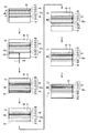
次に、図2(A)を参照して、以下のようにして、デバイス用積層支持基板4に二電極を形成した。デバイス用積層支持基板4の透明半導体層40のp−GaN層47上に、フォトリソグラフィ法によりp−電極用レジストマスク(図示せず)を形成し、真空蒸着法により厚さ5nmのNi層および厚さ11nmのAu層をこの順に形成した後、p−電極用レジストマスクを除去することにより不要部分の電極材料を除去することにより、p−電極80を形成した。
5. Next, with reference to FIG. 2 (A), two electrodes were formed on the device multilayer support substrate 4 as described below. A p-electrode resist mask (not shown) is formed by photolithography on the p-GaN layer 47 of the transparent semiconductor layer 40 of the laminated support substrate 4 for devices, and a Ni layer having a thickness of 5 nm is formed by vacuum evaporation. After forming an Au layer having a thickness of 11 nm in this order, an unnecessary portion of the electrode material was removed by removing the p-electrode resist mask, whereby a p-electrode 80 was formed.

次いで、p−電極80およびその周辺領域にフォトリソグラフィ法によりp−電極保護用レジストマスク(図示せず)を形成し、塩素ガスを用いて透明半導体層40のp−GaN層47側の主表面から250nmの深さまでメサエッチングをして、主表面の一部領域において、p−GaN層47、発光層45およびn−GaN層43を除去し、GaNバッファ層41を露出させた。その後、上記のp−電極保護用レジストマスクを除去した。露出されたGaNバッファ層41上に、上記p−電極の形成と同様の方法により、厚さ20nmのTi層および厚さ300nmのAu層で構成されるn−電極90を形成した。p−電極およびn−電極と半導体層とのオーミック接合を取るために、得られた基板を全圧が1気圧で酸素が0.4体積%の窒素/酸素雰囲気中500℃でアニールした。こうして、二電極付のデバイス用積層支持基板4Aが得られた。この後、図示しないが、p−電極およびn−電極のそれぞれの上に、リフトオフ法により、厚さ20nmのTi層および厚さ300nmのAu層で構成されるパッド電極層を形成してもよい。   Next, a p-electrode protecting resist mask (not shown) is formed on the p-electrode 80 and its peripheral region by photolithography, and the main surface of the transparent semiconductor layer 40 on the p-GaN layer 47 side using chlorine gas. The mesa etching was performed to a depth of 250 nm to remove the p-GaN layer 47, the light emitting layer 45, and the n-GaN layer 43 in a partial region of the main surface, and the GaN buffer layer 41 was exposed. Thereafter, the p-electrode protecting resist mask was removed. On the exposed GaN buffer layer 41, an n-electrode 90 composed of a 20 nm thick Ti layer and a 300 nm thick Au layer was formed by the same method as the formation of the p-electrode. In order to obtain an ohmic junction between the p-electrode and the n-electrode and the semiconductor layer, the obtained substrate was annealed at 500 ° C. in a nitrogen / oxygen atmosphere having a total pressure of 1 atm and oxygen of 0.4 vol%. Thus, a laminated support substrate 4A for devices with two electrodes was obtained. Thereafter, although not shown, a pad electrode layer composed of a 20 nm thick Ti layer and a 300 nm thick Au layer may be formed on each of the p-electrode and the n-electrode by a lift-off method. .

上記のように、半導体デバイスを形成するためには高温のアニールが必要となる。半導体デバイスを作製するためのデバイス用積層支持基板において、Ga含有透明支持基板10、GaN層30aおよび透明半導体層40が、化学種が異なり熱膨張係数が異なる材料であれば接合界面での剥がれ、あるいはGaN層30aおよび透明半導体層40などにクラックなどが生じるおそれがあるが、Ga含有透明支持基板10(GaN支持基板)および透明半導体層40(GaNバッファ層41、n−GaN層43、3対のInGaN層およびGaN層からなる多重量子井戸層である発光層45、およびp−GaN層47)が、GaN層30aと同一または近似する化学種で構成され、それらの基板および層の熱膨張係数が互いに同一または近似しているため、接合界面での剥がれ、GaN層30aおよび透明半導体層40などのクラックなどが防止できる。   As described above, high temperature annealing is required to form a semiconductor device. In the laminated support substrate for a device for producing a semiconductor device, if the Ga-containing transparent support substrate 10, the GaN layer 30a, and the transparent semiconductor layer 40 are materials having different chemical species and different thermal expansion coefficients, peeling at the bonding interface, Alternatively, cracks or the like may occur in the GaN layer 30a and the transparent semiconductor layer 40, but the Ga-containing transparent support substrate 10 (GaN support substrate) and the transparent semiconductor layer 40 (GaN buffer layer 41, n-GaN layer 43, 3 pairs) The light emitting layer 45 and the p-GaN layer 47), which are multiple quantum well layers composed of InGaN layers and GaN layers, are made of the same or similar chemical species as the GaN layer 30a, and the thermal expansion coefficients of those substrates and layers Are the same or approximate to each other, so that peeling at the bonding interface, GaN layer 30a, transparent semiconductor layer 40, etc. Such as the rack can be prevented.

一方、GaNの基板は非常に高価であるため、最終製品としての半導体デバイスの単価を下げるためには、以下に説明するように、デバイス用積層支持基板からGaN支持基板(Ga含有透明支持基板10)を分離する必要がある。以下に説明する方法により、分離されたGaN支持基板(Ga含有透明支持基板10)は、その主表面の処理を行うことにより、再びGaN支持基板として利用できる。このように、1枚のGaN基板を繰り返し使用することにより、最終製品としての半導体デバイスの単価を下げることが可能になる。   On the other hand, since a GaN substrate is very expensive, in order to lower the unit price of a semiconductor device as a final product, as described below, a laminated support substrate for devices is changed from a GaN support substrate (Ga-containing transparent support substrate 10). ) Must be separated. The separated GaN support substrate (Ga-containing transparent support substrate 10) can be used again as a GaN support substrate by treating the main surface by the method described below. Thus, by repeatedly using one GaN substrate, the unit price of the semiconductor device as the final product can be reduced.

6.二電極付のデバイス用積層ウエハの作製工程
次に、図2(B)を参照して、二電極付のデバイス用積層支持基板4Aのp−電極80およびn−電極90の形成面に接着剤51をスピン塗布し、真空中で200℃に加熱された雰囲気下で、ウエハボンダを用いて、仮支持用サファイア板(仮支持基材50)を貼り付けた。かかる接着剤51には、後工程において、ウエハから仮支持用サファイア板を分離することを考慮して、200℃に加熱することで再度軟化させられるもの、たとえばBrewer Sciences社製WaferBond HT−10,10などを選んだ。
6). Next, referring to FIG. 2B, an adhesive is formed on the formation surface of the p-electrode 80 and the n-electrode 90 of the laminated support substrate 4A for devices with two electrodes. 51 was spin-coated, and a temporary support sapphire plate (temporary support base material 50) was attached using a wafer bonder in an atmosphere heated to 200 ° C. in a vacuum. The adhesive 51 can be softened again by heating to 200 ° C. in consideration of separating the temporary support sapphire plate from the wafer in a later process, for example, Wafer Bond HT-10 manufactured by Brewer Sciences, 10 was chosen.

次いで、上記の仮支持用サファイア板(仮支持基材50)が貼り付けられた二電極付のデバイス用積層支持基板4Aをレーザアニール装置(図示せず)にセットした。このレーザアニール装置は、Nd:YAGレーザとLiB35 SHG結晶を用いて、波長532nmの緑色レーザパルスを発生できる。このレーザアニール装置は元来、上記の波長の光を、アモルファスシリコンに吸収させることにより、アモルファスシリコンを数百℃〜千数百℃程度まで急加熱し、ポリシリコンへと変化させるための装置である。 Next, the laminated support substrate 4A for devices with two electrodes to which the sapphire plate for temporary support (temporary support base material 50) was attached was set in a laser annealing apparatus (not shown). This laser annealing apparatus can generate a green laser pulse having a wavelength of 532 nm using an Nd: YAG laser and a LiB 3 O 5 SHG crystal. This laser annealing apparatus is originally an apparatus for rapidly heating amorphous silicon to several hundred to several hundreds of degrees Celsius by absorbing light of the above wavelength into amorphous silicon, and changing it to polysilicon. is there.

上記のレーザアニール装置を用いて、出力が0.2W、繰り返し周期が10kHz、パルス幅が10ns、アモルファスシリコン層上のスポットサイズが直径25nm、スキャンスピードが100mm/sの条件で、二電極付のデバイス用積層支持基板4AのGaN支持基板(Ga含有透明支持基板10)側からレーザを照射し、直径2インチの二電極付のデバイス用積層支持基板4AのGaN支持基板上を順次スキャンした。上記の波長532nmの光は、GaN支持基板(Ga含有透明支持基板10)、二酸化シリコン層(第1の透明層23および第2の透明層25)、GaN層30a、透明半導体層40、接着剤51、および仮支持サファイア板(仮支持基材50)などでは吸収されず、アモルファスシリコン層(光熱変換層21)でのみ効率よく吸収された。これにより、アモルファスシリコン層(光熱変換層21)の温度は急激に上昇した。   Using the laser annealing apparatus described above, two electrodes are attached under the conditions that the output is 0.2 W, the repetition period is 10 kHz, the pulse width is 10 ns, the spot size on the amorphous silicon layer is 25 nm in diameter, and the scan speed is 100 mm / s. Laser was irradiated from the GaN support substrate (Ga-containing transparent support substrate 10) side of the device multilayer support substrate 4A, and the GaN support substrate of the device multilayer support substrate 4A with a two-electrode diameter of 2 inches was sequentially scanned. The light having a wavelength of 532 nm is emitted from a GaN support substrate (Ga-containing transparent support substrate 10), a silicon dioxide layer (first transparent layer 23 and second transparent layer 25), a GaN layer 30a, a transparent semiconductor layer 40, and an adhesive. 51 and the temporary support sapphire plate (temporary support base material 50) and the like were not absorbed, but were efficiently absorbed only by the amorphous silicon layer (photothermal conversion layer 21). Thereby, the temperature of the amorphous silicon layer (photothermal conversion layer 21) increased rapidly.

その結果、アモルファスシリコン層(光熱変換層21)の近距離に位置するGaN支持基板(Ga含有透明支持基板10)における中間層20との貼り合わせ面は、その面の温度が900℃を超え、金属Gaと窒素(N2)ガスに熱分解された。一方、GaN層30aにおける中間層20との貼り合わせ面においては、熱分解温度には至らなかった。これは、GaN層30aとアモルファスシリコン層(光熱変換層21)との間には、GaN(熱伝導率が約100W・m-1・K-1)に比べて熱伝導率の低い二酸化シリコン(熱伝導率が約10W・m-1・K-1)で形成された厚さ230nmの二酸化シリコン層(第1の透明層23)が介在しているため、アモルファスシリコン層(光熱変換層21)で発生した熱量の大半がGaN支持基板(Ga含有透明支持基板10)側に拡散するため、GaN層30aは熱分解温度には至らなかったものと考えられる。また、同様の理由から、接着剤51部分の温度は100℃以下に抑えられ、接着剤51の軟化ないし炭化などの変質は生じなかった。このようにして、GaN支持基板(Ga含有透明支持基板10)における中間層20との貼り合わせ面にのみ金属Ga60を析出させることができた。 As a result, the bonding surface with the intermediate layer 20 in the GaN support substrate (Ga-containing transparent support substrate 10) located at a short distance of the amorphous silicon layer (photothermal conversion layer 21) has a surface temperature exceeding 900 ° C., Pyrolysis into metal Ga and nitrogen (N 2 ) gas. On the other hand, the thermal decomposition temperature was not reached on the bonding surface of the GaN layer 30a with the intermediate layer 20. This is because silicon dioxide (having a thermal conductivity lower than that of GaN (having a thermal conductivity of about 100 W · m −1 · K −1 ) between the GaN layer 30a and the amorphous silicon layer (photothermal conversion layer 21) ( Since a silicon dioxide layer (first transparent layer 23) having a thickness of 230 nm formed with a thermal conductivity of about 10 W · m −1 · K −1 ) is interposed, an amorphous silicon layer (photothermal conversion layer 21) It can be considered that the GaN layer 30a did not reach the thermal decomposition temperature because most of the amount of heat generated in the above was diffused to the GaN support substrate (Ga-containing transparent support substrate 10) side. For the same reason, the temperature of the adhesive 51 portion was suppressed to 100 ° C. or less, and the adhesive 51 was not softened or carbonized. Thus, the metal Ga60 could be deposited only on the bonding surface of the GaN support substrate (Ga-containing transparent support substrate 10) with the intermediate layer 20.

次いで、図2(C)を参照して、上記の金属Ga60が析出した二電極付のデバイス用積層支持基板4Aを、60℃のホットプレート(図示せず)に置いて、金属Ga(融点が29.8℃)を融解させた状態でGaN支持基板を滑らせる(スライドオフする)ことにより、中間層20からGaN支持基板(Ga含有透明支持基板10)を分離した。こうして、透明半導体層40、GaN層30aおよび中間層20を含む二電極付のデバイス用積層ウエハ5Aが得られた。なお、分離されたGaN支持基板は、主表面を研磨およびエッチングなどの処理をすることにより、再度利用できる。   Next, referring to FIG. 2C, the above-mentioned laminated support substrate for devices 4A with two electrodes on which the metal Ga60 is deposited is placed on a hot plate (not shown) at 60 ° C. The GaN support substrate (Ga-containing transparent support substrate 10) was separated from the intermediate layer 20 by sliding (sliding off) the GaN support substrate in a melted state (29.8 ° C.). Thus, a laminated wafer for devices 5A with two electrodes including the transparent semiconductor layer 40, the GaN layer 30a, and the intermediate layer 20 was obtained. Note that the separated GaN support substrate can be reused by subjecting the main surface to a treatment such as polishing and etching.

7.二電極付の透明半導体層積層ウエハの作製工程
次に、図2(D)を参照して、二電極付のデバイス用積層ウエハ5Aの中間層20上の金属Ga60を塩酸により洗浄し、中間層20(二酸化シリコン層および一部がポリシリコン化したアモルファスシリコン層)を、フッ酸硝酸混合溶液を用いたウェットエッチングにより、除去した。こうして、透明半導体層40およびGaN層30aを含む二電極付の透明半導体層積層ウエハ6Aが得られた。
7). Step of Producing Transparent Semiconductor Layer Laminated Wafer with Two Electrodes Next, referring to FIG. 2D, the metal Ga60 on the intermediate layer 20 of the laminated wafer for devices 5A with two electrodes is washed with hydrochloric acid to obtain an intermediate layer. 20 (a silicon dioxide layer and an amorphous silicon layer partially polysiliconized) was removed by wet etching using a hydrofluoric acid nitric acid mixed solution. Thus, a transparent semiconductor layer laminated wafer 6A with two electrodes including the transparent semiconductor layer 40 and the GaN layer 30a was obtained.

8.半導体デバイスの作製工程
次に、図2(E)を参照して、以下のようにして、二電極付の透明半導体積層積層ウエハ6AのGaN層30aに、別途準備した透明半導体層積層ウエハ支持基板70を貼り合わせた。
8). Next, referring to FIG. 2E, a transparent semiconductor layer laminated wafer supporting substrate prepared separately on the GaN layer 30a of the transparent semiconductor laminated wafer 6A with two electrodes as described below with reference to FIG. 70 was bonded.

ここで、準備された透明半導体層積層ウエハ支持基板70としては、厚さ150μmのサファイア基板であった。貼り合わせは、二電極付の透明半導体層積層ウエハ6AのGaN層30aの主表面を洗浄した後に、プラズマエッチング装置にいれて、窒素プラズマ(プラズマ条件は、RFが100W、N2ガス流量が50sccm、チャンバ圧力13.3Paであった)に曝して主表面を清浄にした。サファイア基板(透明半導体層積層ウエハ支持基板70)も、その主表面を洗浄した後に、酸素プラズマ(プラズマ条件は、RFが100W、O2ガス流量が50sccm、チャンバ圧力が6.7Paであった)で主表面を清浄にした。二電極付の透明半導体層積層ウエハ6Aとサファイア基板(透明半導体層積層ウエハ支持基板70)とを貼り合わせた後に、大気中でウエハボンダを用いて7MPaの荷重で押しつけて、接合させて貼り合わせた。 Here, the prepared transparent semiconductor layer laminated wafer support substrate 70 was a sapphire substrate having a thickness of 150 μm. For the bonding, after cleaning the main surface of the GaN layer 30a of the transparent semiconductor layer laminated wafer 6A with two electrodes, it is put into a plasma etching apparatus, and nitrogen plasma (the plasma conditions are RF 100W and N 2 gas flow rate 50sccm). The main surface was cleaned by exposure to a chamber pressure of 13.3 Pa.). The main surface of the sapphire substrate (transparent semiconductor layer laminated wafer support substrate 70) was also cleaned, and then oxygen plasma (the plasma conditions were RF of 100 W, O 2 gas flow rate of 50 sccm, and chamber pressure of 6.7 Pa) To clean the main surface. After the two-electrode transparent semiconductor layer laminated wafer 6A and the sapphire substrate (transparent semiconductor layer laminated wafer support substrate 70) were bonded together, they were pressed and bonded by using a wafer bonder in the air with a load of 7 MPa. .

次いで、図2(F)を参照して、上記の貼り合わせ基板をホットプレートで接着剤の軟化温度である200℃まで加熱して、上記の貼り合わせ基板から仮支持用サファイア板(仮支持基材50)をスライドオフさせて取り除いた。透明半導体層40上のp−電極80およびn−電極90側に残った接着剤は専用のリムーバで除去した。   Next, referring to FIG. 2 (F), the bonded substrate is heated to 200 ° C., which is the softening temperature of the adhesive, with a hot plate, and the sapphire plate for temporary support (temporary support base) is heated from the bonded substrate. The material 50) was slid off and removed. The adhesive remaining on the p-electrode 80 and n-electrode 90 side on the transparent semiconductor layer 40 was removed with a dedicated remover.

上記の工程により、LED(発光ダイオード)である半導体デバイス7が得られた。かかる半導体デバイスにおいて、以降は一般的な素子化工程(スクライブ、ブレーク、ダイボンド、ワイヤボンドなどの諸工程)が適用できる。   The semiconductor device 7 which is LED (light emitting diode) was obtained by said process. In such semiconductor devices, general elementalization processes (processes such as scribe, break, die bond, and wire bond) can be applied thereafter.

(実施例2)
1.デバイス用積層支持基板までの作製工程
図1(A)〜(D)を参照して、実施例1と同様にして、デバイス用積層支持基板4を得た。
(Example 2)
1. Manufacturing Process Up to Device Multilayer Support Substrate With reference to FIGS. 1A to 1D, a device multilayer support substrate 4 was obtained in the same manner as in Example 1.

2.一電極付のデバイス用積層支持基板の作製工程
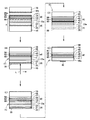
次に、図3(A)を参照して、デバイス用積層支持基板4の透明半導体層40のp−GaN層47上の全面に、真空蒸着法により、p−電極80として、Ni/Au電極(具体的には、厚さ5nmのNi層および厚さ11nmのAu層で構成される電極)を形成した。こうして、一電極付のデバイス用積層支持基板4Bが得られた。
2. Next, referring to FIG. 3A, a vacuum deposition method is performed on the entire surface of the transparent semiconductor layer 40 of the device multilayer support substrate 4 on the p-GaN layer 47 with reference to FIG. Thus, a Ni / Au electrode (specifically, an electrode composed of a Ni layer having a thickness of 5 nm and an Au layer having a thickness of 11 nm) was formed as the p-electrode 80. Thus, a laminated support substrate 4B for a device with one electrode was obtained.

3.一電極付のデバイス用積層ウエハの作製工程
次に、図3(B)〜(C)を参照して、一電極付のデバイス用積層支持基板4Bのp−電極80上に、接着剤51を介在させて仮支持基材50をさせた後、実施例1と同様にして、デバイス用積層支持基板4BからGaN支持基板(Ga含有透明支持基板10)をスライドオフさせた。こうして、一電極付のデバイス用積層ウエハ5Bが得られた。
3. Next, referring to FIGS. 3B to 3C, an adhesive 51 is applied on the p-electrode 80 of the laminated support substrate for a device 4B with one electrode. After interposing the temporary support base material 50, the GaN support substrate (Ga-containing transparent support substrate 10) was slid off from the device multilayer support substrate 4B in the same manner as in Example 1. Thus, a laminated wafer for devices 5B with one electrode was obtained.

4.一電極付の透明半導体層積層ウエハの作製工程
次に、図3(D)を参照して、実施例1と同様にして、一電極付のデバイス用積層ウエハ5Bから金属Ga60および中間層20を除去した。こうして、一電極付の透明半導体層積層ウエハ6Bが得られた。
4). Step of Producing Transparent Semiconductor Layer Laminated Wafer with One Electrode Next, referring to FIG. 3D, in the same manner as in Example 1, the metal Ga 60 and the intermediate layer 20 are formed from the laminated wafer for devices 5B with one electrode. Removed. Thus, a transparent semiconductor layer laminated wafer 6B with one electrode was obtained.

5.半導体デバイスの作製方法
次に、図3(E)を参照して、一電極付の透明半導体層積層ウエハ6BのGa層30aの主表面(N原子表面)の全面に、真空蒸着法により、n−電極90としてTi/Al電極(具体的には、厚さ20nmのTi層および厚さ300nmのAu層で構成される電極)を形成した。次いで、n電極の上に、真空蒸着法により、導電性接着層95aとしてTi/Al層(具体的には、厚さ20nmのTi層および厚さ300nmのAu層)で構成される貼り合わせ用パッド電極層を形成した。
5. Next, referring to FIG. 3 (E), the entire surface of the main surface (N atom surface) of the Ga layer 30a of the transparent semiconductor layer laminated wafer 6B with one electrode is formed by vacuum evaporation. A Ti / Al electrode (specifically, an electrode composed of a 20 nm thick Ti layer and a 300 nm thick Au layer) was formed as the electrode 90. Next, on the n-electrode, by a vacuum vapor deposition method, a conductive adhesive layer 95a is composed of a Ti / Al layer (specifically, a Ti layer having a thickness of 20 nm and an Au layer having a thickness of 300 nm). A pad electrode layer was formed.

次いで、透明半導体層積層ウエハ支持基板70として、導電性基板であるP(リン)を1×1019cm-3と高濃度にドープしたn型導電性Si基板を準備した。このn型導電性Si基板の主表面に、真空蒸着法により、導電性接着層95bとしてTi/Al層(具体的には、厚さ20nmのTi層および厚さ300nmのAu層で構成される層)で構成される貼り合わせ用パッド電極層を形成した。 Next, an n-type conductive Si substrate doped with P (phosphorus), which is a conductive substrate, at a high concentration of 1 × 10 19 cm −3 was prepared as the transparent semiconductor layer laminated wafer support substrate 70. On the main surface of this n-type conductive Si substrate, a Ti / Al layer (specifically, a Ti layer having a thickness of 20 nm and an Au layer having a thickness of 300 nm is formed as a conductive adhesive layer 95b by vacuum deposition. Layer electrode) for bonding was formed.

次に、図3(F)を参照して、一電極付の透明半導体層積層ウエハ6Bに形成された貼り合わせ用パッド電極層(導電性接着層95a)と、n型導電性Si基板(透明半導体層積層ウエハ支持基板70)に形成された貼り合わせ用パッド電極層(導電性接着層95b)と、を重ね合わせて、真空状態に保ったウエハボンダで3MPaの荷重で押しつけながら、400℃に加熱することにより、接合させて貼り合わせた。   Next, referring to FIG. 3F, a bonding pad electrode layer (conductive adhesive layer 95a) formed on the transparent semiconductor layer laminated wafer 6B with one electrode, and an n-type conductive Si substrate (transparent The laminated pad electrode layer (conductive adhesive layer 95b) formed on the semiconductor layer laminated wafer supporting substrate 70) is superposed and heated to 400 ° C. while being pressed with a 3 MPa load with a wafer bonder kept in a vacuum state. By joining, it bonded and bonded together.

次いで、貼り合わせ後に、n型導電性Si基板(透明半導体層積層ウエハ支持基板70)の裏面を研磨および洗浄して露出させた清浄面に、真空蒸着法により、n−パッド電極層92としてTi/Auパッド電極層(具体的には、厚さ20nmのTi層および厚さ300nmのAu層で構成されるパッド電極層)を形成した。   Next, after bonding, the back surface of the n-type conductive Si substrate (transparent semiconductor layer laminated wafer support substrate 70) is polished and washed to expose a cleaned surface as an n-pad electrode layer 92 by vacuum deposition. / An Au pad electrode layer (specifically, a pad electrode layer composed of a 20 nm thick Ti layer and a 300 nm thick Au layer) was formed.

次いで、図3(G)を参照して、上記の貼り合わせ基板をホットプレートで接着剤の軟化温度である200℃まで加熱して、上記の貼り合わせ基板から仮支持用サファイア板(仮支持基材50)をスライドオフさせて取り除いた。透明半導体層40上のp−電極80側に残った接着剤は専用のリムーバで除去した。   Next, referring to FIG. 3G, the bonded substrate is heated to 200 ° C., which is the softening temperature of the adhesive, with a hot plate, and the sapphire plate for temporary support (temporary support substrate) is heated from the bonded substrate. The material 50) was slid off and removed. The adhesive remaining on the p-electrode 80 side on the transparent semiconductor layer 40 was removed with a dedicated remover.

さらに、p−電極80、n−電極90およびn−パッド電極層92のオーミック化のために、上記の貼り合わせ基板を全圧が1気圧で酸素が0.4体積%の窒素/酸素雰囲気中500℃でアニールした。   Further, in order to make the p-electrode 80, the n-electrode 90, and the n-pad electrode layer 92 ohmic, the above bonded substrate is placed in a nitrogen / oxygen atmosphere with a total pressure of 1 atm and oxygen of 0.4 vol%. Annealed at 500 ° C.

上記の工程により、LED(発光ダイオード)である半導体デバイス7が得られた。かかる半導体デバイスにおいて、以降は一般的な素子化工程(スクライブ、ブレーク、ダイボンド、ワイヤボンドなどの諸工程)が適用できる。   The semiconductor device 7 which is LED (light emitting diode) was obtained by said process. In such semiconductor devices, general elementalization processes (processes such as scribe, break, die bond, and wire bond) can be applied thereafter.

なお、本実施例においては、透明半導体層積層ウエハ支持基板70である導電性基板は透明基板であってもよい。かかる場合には、n−電極、貼り合わせ用パッド電極層およびn−パッド電極層として、ITO(インジウムスズ酸化物)をはじめとする透明導電性材料を用いることにより、支持基板側から光を取り出す様な実装(いわゆる、p−down実装)も可能となる。   In the present embodiment, the conductive substrate which is the transparent semiconductor layer laminated wafer support substrate 70 may be a transparent substrate. In such a case, light is extracted from the support substrate side by using a transparent conductive material such as ITO (indium tin oxide) as the n-electrode, the bonding pad electrode layer, and the n-pad electrode layer. Such mounting (so-called p-down mounting) is also possible.

(実施例3)
1.デバイス用積層支持基板までの作製工程
図1(A)〜(D)を参照して、実施例1と同様にして、デバイス用積層支持基板4を得た。
(Example 3)
1. Manufacturing Process Up to Device Multilayer Support Substrate With reference to FIGS. 1A to 1D, a device multilayer support substrate 4 was obtained in the same manner as in Example 1.

2.デバイス用積層支持基板への透明半導体層積層ウエハ支持基板を貼り合わせ工程
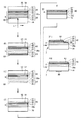
次に、図4(A)を参照して、デバイス用積層支持基板4の透明半導体層40のp−GaN層47上の全面に、真空蒸着法により、Ni/Au電極(具体的には、厚さ5nmのNi層および厚さ11nmのAu層で構成される電極)を形成し、この貼り合わせ基板を窒素/酸素雰囲気中500℃でアニールすることにより、p−電極80を形成した。
2. Next, referring to FIG. 4A, the transparent semiconductor layer laminated wafer support substrate is bonded to the device laminated support substrate. On the p-GaN layer 47 of the transparent semiconductor layer 40 of the device laminated support substrate 4 A Ni / Au electrode (specifically, an electrode composed of a Ni layer having a thickness of 5 nm and an Au layer having a thickness of 11 nm) is formed on the entire surface by vacuum evaporation, and the bonded substrate is placed in a nitrogen / oxygen atmosphere. The p-electrode 80 was formed by annealing at 500 ° C.

次いで、p−電極80上に真空蒸着法により厚さ50nmのAg層83を形成し、その上にスパッタ法により厚さ200nmのITO(インジウムスズ酸化物)層84を形成し、その上に真空蒸着法により導電性接着層85aとして貼り合わせ用Ti/Auパッド電極層を形成した。   Next, an Ag layer 83 having a thickness of 50 nm is formed on the p-electrode 80 by a vacuum evaporation method, and an ITO (indium tin oxide) layer 84 having a thickness of 200 nm is formed thereon by a sputtering method. A Ti / Au pad electrode layer for bonding was formed as the conductive adhesive layer 85a by vapor deposition.

一方で、主表面に貼り合わせ用Ti/Auパッド電極層(導電性接着層85b)を形成した透明半導体層積層ウエハ支持基板70を準備した。透明半導体層積層ウエハ支持基板70としては、導電性支持基板であるB(ホウ素)を1×1019cm-3と高濃度にドープしたp型導電型Si基板を用いた。 On the other hand, a transparent semiconductor layer laminated wafer support substrate 70 in which a bonding Ti / Au pad electrode layer (conductive adhesive layer 85b) was formed on the main surface was prepared. As the transparent semiconductor layer laminated wafer support substrate 70, a p-type conductivity Si substrate doped with B (boron), which is a conductive support substrate, at a high concentration of 1 × 10 19 cm −3 was used.

次いで、デバイス用積層支持基板4に形成された貼り合わせ用Ti/Auパッド電極層(導電性接着層85a)と、透明半導体層積層ウエハ支持基板70に形成された貼り合わせ用Ti/Auパッド電極層(導電性接着層85b)と、を重ね合わせてウエハボンダで350℃で4MPaの条件で加熱加圧して接合して貼り合わせた。   Next, a bonding Ti / Au pad electrode layer (conductive adhesive layer 85a) formed on the device laminated support substrate 4 and a bonding Ti / Au pad electrode formed on the transparent semiconductor layer laminated wafer support substrate 70 The layers (the conductive adhesive layer 85b) were superposed and bonded together by heating and pressing with a wafer bonder at 350 ° C. under the condition of 4 MPa.

3.支持基板付のデバイス用積層ウエハの作製工程
次に、図4(B)〜(C)を参照して、透明半導体層積層ウエハ支持基板70が貼り合わされたデバイス用積層支持基板4Cから、実施例1と同様にして、Ga含有透明支持基板10を分離した。こうして、支持基板付のデバイス用積層ウエハ5Cが得られた。
3. Next, referring to FIGS. 4B to 4C, a device laminated support substrate 4 </ b> C to which a transparent semiconductor layer laminated wafer support substrate 70 is bonded is described with reference to FIGS. In the same manner as in Example 1, the Ga-containing transparent support substrate 10 was separated. Thus, a laminated wafer for devices 5C with a supporting substrate was obtained.

4.支持基板付の透明半導体層積層ウエハの作製工程
次に、図4(D)を参照して、支持基板付のデバイス用積層ウエハ5Cから、実施例1と同様にして、金属Ga60および中間層20が分離除去した。こうして、支持基板付の透明半導体層積層ウエハ6が得られた。
4). Step of Producing Transparent Semiconductor Layer Laminated Wafer with Support Substrate Next, referring to FIG. 4D, from the device laminated wafer 5C with a support substrate, in the same manner as in Example 1, the metal Ga 60 and the intermediate layer 20 Separated and removed. Thus, a transparent semiconductor layer laminated wafer 6 with a support substrate was obtained.

5.半導体デバイスの作製工程
次に、図4(E)を参照して、支持基板付の透明半導体層積層ウエハ6のp型導電型Si基板(透明半導体層積層ウエハ支持基板)上に、真空蒸着法により、p−パッド電極層86としてTi/Auパッド電極層(具体的には、厚さ20nmのTi層および厚さ300nmのAu層で構成されるパッド電極層)を形成した。また、支持基板付の透明半導体層積層ウエハ6のGaN層30a上に、真空蒸着法およびリフトオフ法により、n−電極90としてTi/Au電極(具体的には、厚さ20nmのTi層および厚さ300nmのAu層で構成される電極)を形成した。p−パッド電極層86およびp−電極90と半導体層とのオーミック接合を取るために、これらの電極が形成された支持基板付の透明半導体層積層ウエハ6を、窒素雰囲気中500℃でアニールした。こうして、LEDである半導体デバイス7が得られた。以降は一般的な素子化工程(スクライブ、ブレーク、ダイボンド、ワイヤボンドなどの諸工程)が適用できる。
5. Next, referring to FIG. 4E, a vacuum deposition method is performed on a p-type conductivity Si substrate (transparent semiconductor layer laminated wafer supporting substrate) of a transparent semiconductor layer laminated wafer 6 with a supporting substrate. Thus, a Ti / Au pad electrode layer (specifically, a pad electrode layer composed of a 20 nm thick Ti layer and a 300 nm thick Au layer) was formed as the p-pad electrode layer 86. Further, a Ti / Au electrode (specifically, a 20 nm-thick Ti layer and a thickness) is formed on the GaN layer 30a of the transparent semiconductor layer laminated wafer 6 with a support substrate by a vacuum deposition method and a lift-off method. An electrode composed of a 300 nm thick Au layer) was formed. In order to obtain an ohmic junction between the p-pad electrode layer 86 and the p-electrode 90 and the semiconductor layer, the transparent semiconductor layer laminated wafer 6 with a supporting substrate on which these electrodes were formed was annealed at 500 ° C. in a nitrogen atmosphere. . Thus, a semiconductor device 7 which is an LED was obtained. Thereafter, a general element forming process (processes such as scribe, break, die bond, wire bond) can be applied.

(実施例4)
本実施例は、透明半導体層積層ウエハ支持基板の熱膨係数がGaNの熱膨張係数と同一または近似している場合に適用される。
Example 4
This embodiment is applied when the thermal expansion coefficient of the transparent semiconductor layer laminated wafer supporting substrate is the same as or close to the thermal expansion coefficient of GaN.

1.デバイス用積層支持基板までの作製工程
図1(A)〜(D)を参照して、実施例1と同様にして、デバイス用積層支持基板4を得た。
1. Manufacturing Process Up to Device Multilayer Support Substrate With reference to FIGS. 1A to 1D, a device multilayer support substrate 4 was obtained in the same manner as in Example 1.

2.デバイス用積層ウエハの作製工程
次に、図5(A)および(B)を参照して、デバイス用積層支持基板4の中間層20のp−GaN層47上に、接着剤51を介在させて仮支持基材50をさせた後、実施例1と同様にして、デバイス用積層支持基板4からGaN支持基板(Ga含有透明支持基板10)をスライドオフさせた。こうして、デバイス用積層ウエハ5が得られた。
2. Next, referring to FIGS. 5A and 5B, an adhesive 51 is interposed on the p-GaN layer 47 of the intermediate layer 20 of the laminated support substrate 4 for devices. After making the temporary support base material 50, the GaN support substrate (Ga-containing transparent support substrate 10) was slid off from the device multilayer support substrate 4 in the same manner as in Example 1. Thus, the device laminated wafer 5 was obtained.

3.透明半導体層積層ウエハの作製工程
次に、図5(C)を参照して、実施例1と同様にして、一電極付のデバイス用積層ウエハ5Bから金属Ga60および中間層20を除去した。こうして、透明半導体層積層ウエハ6が得られた。
3. Next, with reference to FIG. 5C, in the same manner as in Example 1, the metal Ga 60 and the intermediate layer 20 were removed from the device laminated wafer 5B with one electrode. Thus, a transparent semiconductor layer laminated wafer 6 was obtained.

4.半導体デバイスの作製工程
次に、図5(D)を参照して、透明半導体層積層ウエハ6に透明半導体層積層ウエハ支持基板70として透明支持基板であるスピネル基板を貼り合わせた。
4). Next, referring to FIG. 5D, a spinel substrate, which is a transparent support substrate, was bonded to the transparent semiconductor layer stacked wafer 6 as the transparent semiconductor layer stacked wafer support substrate 70.

上記の貼り合わせは、透明半導体層積層ウエハ6のGaN層30aの主表面を洗浄した後に、プラズマエッチング装置にいれて、窒素プラズマ(プラズマ条件は、RFが100W、N2ガス流量が50sccm、チャンバ圧力13.3Paであった)に曝して主表面を清浄にした。スピネル基板(透明半導体層積層ウエハ支持基板70)も、その主表面を洗浄した後に、酸素プラズマ(プラズマ条件は、RFが100W、O2ガス流量が50sccm、チャンバ圧力が6.7Paであった。)で主表面を清浄にした。透明半導体層積層ウエハ6とスピネル基板(透明半導体層積層ウエハ支持基板70)とを貼り合わせた後に、大気中でウエハボンダを用いて7MPaの荷重で押しつけて、接合させて貼り合わせた。その後、この貼り合わせ基板をホットプレートで200℃までゆっくりと昇温させることにより、接合強度を増大させた。 The above bonding is performed by cleaning the main surface of the GaN layer 30a of the transparent semiconductor layer laminated wafer 6 and then putting it in a plasma etching apparatus to form nitrogen plasma (the plasma conditions are RF of 100 W, N 2 gas flow rate of 50 sccm, chamber The main surface was cleaned by exposure to a pressure of 13.3 Pa. The main surface of the spinel substrate (transparent semiconductor layer laminated wafer support substrate 70) was also cleaned, and then oxygen plasma (plasma conditions were RF of 100 W, O 2 gas flow rate of 50 sccm, and chamber pressure of 6.7 Pa). ) To clean the main surface. After the transparent semiconductor layer laminated wafer 6 and the spinel substrate (transparent semiconductor layer laminated wafer support substrate 70) were bonded together, they were pressed and bonded in a pressure of 7 MPa using a wafer bonder in the atmosphere. Thereafter, the bonded substrate was slowly heated up to 200 ° C. with a hot plate to increase the bonding strength.

このとき、図5(E)を参照して、上記の貼り合わせ基板は接着剤の軟化温度である200℃まで加熱されているため、上記の貼り合わせ基板から仮支持用サファイア板(仮支持基材50)をスライドオフさせて取り除いた。透明半導体層40上のp−電極80側に残った接着剤は専用のリムーバで除去した。   At this time, referring to FIG. 5 (E), the bonded substrate is heated to 200 ° C. which is the softening temperature of the adhesive. The material 50) was slid off and removed. The adhesive remaining on the p-electrode 80 side on the transparent semiconductor layer 40 was removed with a dedicated remover.

その後は、通常の電極形成工程、たとえば実施例1の5.二電極付のデバイス用積層支持基板の作製工程に記載されたようなp−電極およびn−電極の形成工程、を用いて、片側にp−電極80およびn−電極90を有する半導体デバイス(図5(F1)を参照)が得られた。   Thereafter, a normal electrode forming process, for example, 5. A semiconductor device having a p-electrode 80 and an n-electrode 90 on one side using a p-electrode and an n-electrode formation process as described in the process for producing a laminated support substrate for a device with two electrodes (FIG. 5 (see F1)).

なお、透明半導体層積層ウエハ支持基板70として透明でかつ導電性の基板を用いる場合は、通常の電極形成工程により、一方側にp−電極80を有し他方側にn−電極90を有する半導体デバイス(図5(F2)を参照)を形成することもできる。   When a transparent and conductive substrate is used as the transparent semiconductor layer laminated wafer support substrate 70, a semiconductor having a p-electrode 80 on one side and an n-electrode 90 on the other side by a normal electrode forming process. A device (see FIG. 5F2) can also be formed.

(実施例5)
中間層20の形成において、第2の透明層25として二酸化シリコン層の厚さを40nmとしたこと以外は、実施例1と同様にして、積層支持基板を作製し、その積層支持基板から積層貼り合わせ基板、エピ成長用積層支持基板、デバイス用積層支持基板、二電極付のデバイス用積層支持基板、二電極付のデバイス用積層ウエハ、二電極付の透明半導体層積層ウエハ、半導体デバイスを順次作製した。実施例1に比べて、透明半導体層40のエピタキシャル成長の際に厚さ60nmのアモルファスシリコン層(光熱変換層)と厚さ40nmの二酸化シリコン層(第2の透明層)との界面において高温によりもたらされる熱膨張係数の違いに起因した剥がれの発生が完全に防止された。レーザ照射による金属Ga60および中間層20の分離除去も問題なく実施できた。これにより、半導体デバイスの歩留まりが向上した。
(Example 5)
In the formation of the intermediate layer 20, a laminated support substrate was prepared in the same manner as in Example 1 except that the thickness of the silicon dioxide layer as the second transparent layer 25 was 40 nm, and the laminated support substrate was laminated and laminated. Laminated substrate, epitaxial growth support substrate, device support substrate, device support substrate with two electrodes, device wafer with two electrodes, transparent semiconductor layer wafer with two electrodes, and semiconductor device did. Compared with the first embodiment, the epitaxial growth of the transparent semiconductor layer 40 is caused by the high temperature at the interface between the amorphous silicon layer (photothermal conversion layer) having a thickness of 60 nm and the silicon dioxide layer (second transparent layer) having a thickness of 40 nm. The occurrence of peeling due to the difference in thermal expansion coefficient was completely prevented. Separation and removal of the metal Ga60 and the intermediate layer 20 by laser irradiation could be performed without any problem. Thereby, the yield of semiconductor devices was improved.

(実施例6)
中間層20の形成において、第2の透明層25として二酸化シリコン層の厚さを40nmとしたこと以外は、実施例2と同様にして、積層支持基板を作製し、その積層支持基板から積層貼り合わせ基板、エピ成長用積層支持基板、デバイス用積層支持基板、一電極付のデバイス用積層支持基板、一電極付のデバイス用積層ウエハ、一電極付の透明半導体層積層ウエハ、半導体デバイスを順次作製した。実施例2に比べて、透明半導体層40のエピタキシャル成長の際に厚さ60nmのアモルファスシリコン層(光熱変換層)と厚さ40nmの二酸化シリコン層(第2の透明層)との界面において高温によりもたらされる熱膨張係数の違いに起因した剥がれの発生が完全に防止された。レーザ照射による金属Ga60および中間層20の分離除去も問題なく実施できた。これにより、半導体デバイスの歩留まりが向上した。
(Example 6)
In the formation of the intermediate layer 20, a laminated support substrate was prepared in the same manner as in Example 2 except that the thickness of the silicon dioxide layer as the second transparent layer 25 was 40 nm, and the laminated support substrate was laminated and laminated. Laminated substrate, epitaxial growth support substrate, device support substrate with one electrode, device support substrate with one electrode, device wafer with one electrode, transparent semiconductor layer laminate wafer with one electrode, and semiconductor device did. Compared with the second embodiment, the epitaxial growth of the transparent semiconductor layer 40 is caused by the high temperature at the interface between the amorphous silicon layer (photothermal conversion layer) having a thickness of 60 nm and the silicon dioxide layer (second transparent layer) having a thickness of 40 nm. The occurrence of peeling due to the difference in thermal expansion coefficient was completely prevented. Separation and removal of the metal Ga60 and the intermediate layer 20 by laser irradiation could be performed without any problem. Thereby, the yield of semiconductor devices was improved.

(実施例7)
中間層20の形成において、第2の透明層25として二酸化シリコン層の厚さを40nmとしたこと以外は、実施例3と同様にして、積層支持基板を作製し、その積層支持基板から積層貼り合わせ基板、エピ成長用積層支持基板、デバイス用積層支持基板、支持基板付のデバイス用積層支持基板、支持基板付のデバイス用積層ウエハ、支持基板付の透明半導体層積層ウエハ、半導体デバイスを順次作製した。実施例3に比べて、透明半導体層40のエピタキシャル成長の際に厚さ60nmのアモルファスシリコン層(光熱変換層)と厚さ40nmの二酸化シリコン層(第2の透明層)との界面において高温によりもたらされる熱膨張係数の違いに起因した剥がれの発生が完全に防止された。レーザ照射による金属Ga60および中間層20の分離除去も問題なく実施できた。これにより、半導体デバイスの歩留まりが向上した。
(Example 7)
In the formation of the intermediate layer 20, a laminated support substrate was produced in the same manner as in Example 3 except that the thickness of the silicon dioxide layer as the second transparent layer 25 was 40 nm, and the laminated support substrate was laminated and laminated. Laminated substrate, epitaxial growth support substrate, device support substrate, device support substrate with support substrate, device support wafer with support substrate, transparent semiconductor layer support wafer with support substrate, semiconductor device did. Compared to Example 3, the epitaxial growth of the transparent semiconductor layer 40 is caused by a high temperature at the interface between the amorphous silicon layer (photothermal conversion layer) having a thickness of 60 nm and the silicon dioxide layer (second transparent layer) having a thickness of 40 nm. The occurrence of peeling due to the difference in thermal expansion coefficient was completely prevented. Separation and removal of the metal Ga60 and the intermediate layer 20 by laser irradiation could be performed without any problem. Thereby, the yield of semiconductor devices was improved.

(実施例8)
中間層20の形成において、第2の透明層25として二酸化シリコン層の厚さを40nmとしたこと以外は、実施例1と同様にして、積層支持基板を作製し、その積層支持基板から積層貼り合わせ基板、エピ成長用積層支持基板、デバイス用積層支持基板、デバイス用積層ウエハ、透明半導体層積層ウエハ、半導体デバイスを順次作製した。実施例1に比べて、透明半導体層40のエピタキシャル成長の際に厚さ60nmのアモルファスシリコン層(光熱変換層)と厚さ40nmの二酸化シリコン層(第2の透明層)との界面において高温によりもたらされる熱膨張係数の違いに起因した剥がれの発生が完全に防止された。レーザ照射による金属Ga60および中間層20の分離除去も問題なく実施できた。これにより、半導体デバイスの歩留まりが向上した。
(Example 8)
In the formation of the intermediate layer 20, a laminated support substrate was prepared in the same manner as in Example 1 except that the thickness of the silicon dioxide layer as the second transparent layer 25 was 40 nm, and the laminated support substrate was laminated and laminated. A laminated substrate, a laminated support substrate for epi growth, a laminated support substrate for devices, a laminated wafer for devices, a transparent semiconductor layer laminated wafer, and a semiconductor device were sequentially produced. Compared with the first embodiment, the epitaxial growth of the transparent semiconductor layer 40 is caused by the high temperature at the interface between the amorphous silicon layer (photothermal conversion layer) having a thickness of 60 nm and the silicon dioxide layer (second transparent layer) having a thickness of 40 nm. The occurrence of peeling due to the difference in thermal expansion coefficient was completely prevented. Separation and removal of the metal Ga60 and the intermediate layer 20 by laser irradiation could be performed without any problem. Thereby, the yield of semiconductor devices was improved.

(実施例9)
本実施例は、本願技術を用いたパワーデバイスの一例としてSBD(ショットキーバリアダイオード)を作製した場合を例示する。
Example 9
In this example, a case where an SBD (Schottky barrier diode) is manufactured as an example of a power device using the present technology is illustrated.

1.エピ成長用積層支持基板までの作製工程
図1(A)〜(C)を参照して、実施例1と同様にして、エピ成長用積層支持基板3を得た。
1. Manufacturing Process Up to Epi-Growing Multilayer Support Substrate With reference to FIGS. 1A to 1C, an epi-growth multi-layer support substrate 3 was obtained in the same manner as in Example 1.

2.デバイス用積層支持基板の作製工程
次に、図6(A)を参照して、エピ成長用積層支持基板3のGaN層30a上に、MOCVD法により、透明半導体層40として、キャリア濃度が1×1018cm-3で厚さ0.5μmのn+−GaNストップ層42と、キャリア濃度が7×1015cm-3で厚さ5μmのn−GaNドリフト層44と、を順次成長させた。こうして、デバイス用積層支持基板4が得られた。
2. Next, referring to FIG. 6A, a carrier concentration of 1 × as the transparent semiconductor layer 40 is formed on the GaN layer 30a of the epitaxial growth support substrate 3 by MOCVD. An n + -GaN stop layer 42 having a thickness of 10 18 cm −3 and a thickness of 0.5 μm and an n-GaN drift layer 44 having a carrier concentration of 7 × 10 15 cm −3 and a thickness of 5 μm were sequentially grown. In this way, the laminated support substrate 4 for devices was obtained.

3.一電極付のデバイス用積層支持基板の作製工程
次に、図6(B)を参照して、デバイス用積層支持基板4のうちの透明半導体層40のn−GaNドリフト層44上に、フォトリソグラフィ、10質量%塩酸水溶液による表面処理、Ni/Au層(具体的には厚さ50nmのNi層および厚さ300nmのAu層で構成される層)のEB蒸着、ならびにリフトオフにより、n−GaNドリフト層44上に直径200μmのショットキー電極81を形成した。こうして、一電極付のデバイス用積層支持基板4Dが得られた。
3. Next, referring to FIG. 6B, photolithography is performed on the n-GaN drift layer 44 of the transparent semiconductor layer 40 in the device multilayer support substrate 4. N-GaN drift by surface treatment with 10% by mass hydrochloric acid aqueous solution, EB deposition of Ni / Au layer (specifically, a layer composed of Ni layer of 50 nm thickness and Au layer of 300 nm thickness), and lift-off A Schottky electrode 81 having a diameter of 200 μm was formed on the layer 44. Thus, a laminated support substrate for a device 4D with one electrode was obtained.

4a.半導体デバイスの作製工程
次に、一例目として、図6(B)〜(C)を参照して、実施例1と同様にして、GaN支持基板(Ga含有透明支持基板10)を透明半導体層積層ウエハ支持基板70に置き換えたタイプのSBDを作製した。具体的には、一電極付のデバイス用積層支持基板4Dのショットキー電極81側を接着剤により仮支持基材に貼り付け、レーザアニール装置を用いてGaN支持基板(Ga含有透明支持基板10)側からレーザを照射して、GaN支持基板(Ga含有透明支持基板10)における中間層20との貼り合わせ面にのみ金属Ga60を析出させた。スライドオフにより、GaN支持基板(Ga含有透明支持基板10)を分離し、さらに中間層20を除去した後、一電極付の透明半導体層積層ウエハ6DのGaN層30aの主表面(N原子表面)の全面に、真空蒸着法により、n−電極90としてTi/Al電極(具体的には、厚さ20nmのTi層および厚さ300nmのAl層で構成される電極)を形成した。その後、透明半導体層積層ウエハ支持基板70としてのP(リン)を1×1019cm-3と高濃度にドープしたn型導電性Si基板の両主表面にオーミック電極93を形成したものを準備して、上記のn−電極90と金属ハンダ71により接合させた。その後、仮支持基材を除去して、図6(C)に示すSBDを完成させた。
4a. Next, as a first example, referring to FIGS. 6B to 6C, a GaN support substrate (Ga-containing transparent support substrate 10) is laminated on a transparent semiconductor layer in the same manner as in Example 1. An SBD of the type replaced with the wafer support substrate 70 was produced. Specifically, the Schottky electrode 81 side of the laminated support substrate 4D for a device with one electrode is attached to a temporary support base material with an adhesive, and a GaN support substrate (Ga-containing transparent support substrate 10) using a laser annealing apparatus. Laser was irradiated from the side to deposit metal Ga60 only on the bonding surface of the GaN support substrate (Ga-containing transparent support substrate 10) with the intermediate layer 20. The GaN support substrate (Ga-containing transparent support substrate 10) is separated by slide-off, and after removing the intermediate layer 20, the main surface (N atom surface) of the GaN layer 30a of the transparent semiconductor layer laminated wafer 6D with one electrode A Ti / Al electrode (specifically, an electrode composed of a 20 nm-thick Ti layer and a 300 nm-thick Al layer) was formed as an n-electrode 90 on the entire surface by vacuum evaporation. Thereafter, a transparent semiconductor layer laminated wafer supporting substrate 70 prepared by forming ohmic electrodes 93 on both main surfaces of an n-type conductive Si substrate doped with P (phosphorus) at a high concentration of 1 × 10 19 cm −3 is prepared. The n-electrode 90 and the metal solder 71 were joined. Thereafter, the temporary support substrate was removed to complete the SBD shown in FIG.

なお、上記SBDの作製と並行して、上記SBDにおいてn型導電性Si基板(透明半導体層積層ウエハ支持基板70)の両主面にオーミック電極93が形成されたものに替えて、n型導電性Ge基板(透明半導体層積層ウエハ支持基板70)の両主表面にオーミック電極93が形成されたもの、Mo薄膜、W薄膜およびTa薄膜のそれぞれを用いたSBDも製作した。   In parallel with the production of the SBD, in the SBD, instead of the n-type conductive Si substrate (transparent semiconductor layer laminated wafer support substrate 70) having the ohmic electrodes 93 formed on both main surfaces, the n-type conductive An SBD using an ohmic electrode 93 formed on both main surfaces of a conductive Ge substrate (transparent semiconductor layer laminated wafer support substrate 70), an Mo thin film, a W thin film, and a Ta thin film was also manufactured.

こうして得られた5種のSBDの特性は、いずれもオン抵抗が1.1mΩ・cm2と低く、電流密度が500A/cm2における順方向電圧Vfは1.3Vと低く、リーク電流密度が1×10-3A/cm2における逆方向耐電圧は350Vと高かった。 As for the characteristics of the five types of SBDs thus obtained, the on-resistance is as low as 1.1 mΩ · cm 2 , the forward voltage Vf is as low as 1.3 V at a current density of 500 A / cm 2 , and the leakage current density is 1 The reverse withstand voltage at × 10 −3 A / cm 2 was as high as 350V.

4b.半導体デバイスの作製工程
続いて二例目として、図6(B)および(D)を参照して、実施例3と同様にして、透明半導体層積層ウエハ支持基板70が透明半導体層40側に配置されたタイプのSBDを作製した。具体的には、一電極付のデバイス用積層支持基板4Dのショットキー電極81周りに、SiO2絶縁層82を形成した後、金属ハンダ71によりn型導電性Si基板(透明半導体層積層ウエハ支持基板70)の両主面にオーミック電極73が形成されたものを接合した。上記と同様に、n型導電性Si基板(透明半導体層積層ウエハ支持基板70)の両主面にオーミック電極73が形成されたものに替えて、n型導電性Ge基板(透明半導体層積層ウエハ支持基板70)の両主表面にオーミック電極73が形成されたもの、Mo薄膜、W薄膜およびTa薄膜を接合させたものも作製した。その後、それぞれについて、接合レーザアニール装置を用いてGaN支持基板(Ga含有透明支持基板10)側からレーザを照射して、GaN支持基板(Ga含有透明支持基板10)における中間層20との貼り合わせ面にのみ金属Ga60を析出させた。スライドオフにより、GaN支持基板(Ga含有透明支持基板10)を分離し、さらに中間層20を除去した後、一電極付の透明半導体層積層ウエハ6DのGa層30aの主表面(N原子表面)の全面に、真空蒸着法により、n−電極90としてTi/Al電極(具体的には、厚さ20nmのTi層および厚さ300nmのAu層で構成される電極)を形成して、図6(C)に示すSBDを完成させた。
4b. Next, as a second example, with reference to FIGS. 6B and 6D, the transparent semiconductor layer laminated wafer support substrate 70 is disposed on the transparent semiconductor layer 40 side in the same manner as in Example 3. The type of SBD was made. Specifically, after a SiO 2 insulating layer 82 is formed around the Schottky electrode 81 of the device laminated support substrate 4D with one electrode, an n-type conductive Si substrate (transparent semiconductor layer laminated wafer support) is formed by the metal solder 71. A substrate 70) having an ohmic electrode 73 formed on both main surfaces was joined. In the same manner as described above, an n-type conductive Ge substrate (transparent semiconductor layer laminated wafer) is used instead of the n-type conductive Si substrate (transparent semiconductor layer laminated wafer support substrate 70) in which ohmic electrodes 73 are formed on both main surfaces. A substrate in which ohmic electrodes 73 are formed on both main surfaces of the support substrate 70), and a Mo thin film, a W thin film, and a Ta thin film are joined. After that, each is irradiated with laser from the GaN support substrate (Ga-containing transparent support substrate 10) side using a bonding laser annealing apparatus, and bonded to the intermediate layer 20 in the GaN support substrate (Ga-containing transparent support substrate 10). Metal Ga60 was deposited only on the surface. The GaN support substrate (Ga-containing transparent support substrate 10) is separated by slide-off, and after the intermediate layer 20 is removed, the main surface (N atom surface) of the Ga layer 30a of the transparent semiconductor layer laminated wafer 6D with one electrode A Ti / Al electrode (specifically, an electrode composed of a 20 nm thick Ti layer and a 300 nm thick Au layer) is formed as an n-electrode 90 by vacuum deposition on the entire surface of FIG. The SBD shown in (C) was completed.

こうして得られた5種のSBDの特性は、いずれもオン抵抗は1.1mΩ・cm2と低く、電流密度が500A/cm2における順方向電圧Vfは1.3Vと低く、リーク電流密度が1×10-3A/cm2における逆方向耐電圧は300Vと高かった。 As for the characteristics of the five types of SBDs thus obtained, the on-resistance is as low as 1.1 mΩ · cm 2 , the forward voltage Vf is as low as 1.3 V at a current density of 500 A / cm 2 , and the leakage current density is 1 The reverse withstand voltage at × 10 −3 A / cm 2 was as high as 300V.

(実施例10)
本実施例は、本願技術を用いたパワーデバイスの一例としてPND(pn接合ダイオード)を作製した場合を例示する。
(Example 10)
This example illustrates the case where a PND (pn junction diode) is manufactured as an example of a power device using the present technology.

1.エピ成長用積層支持基板までの作製工程
図1(A)〜(C)を参照して、実施例1と同様にして、エピ成長用積層支持基板3を得た。
1. Manufacturing Process Up to Epi-Growing Multilayer Support Substrate With reference to FIGS. 1A to 1C, an epi-growth multi-layer support substrate 3 was obtained in the same manner as in Example 1.

2.デバイス用積層支持基板の作製工程
次に、図7(A)を参照して、エピ成長用積層支持基板3のGaN層30a上に、MOCVD法により、透明半導体層40として、厚さ0.5μmのn+−GaNストップ層42(キャリア濃度:1×1018cm-3)、厚さ7μmのn−GaN層46(キャリア濃度:3×1016cm-3)、厚さ0.5μmのp−GaN層48(キャリア濃度:7×1017cm-3)および厚さ75nmのp+−GaNコンタクト層49(Mg濃度:1×1019cm-3)を順次成長させた。こうして、デバイス用積層支持基板4が得られた。
2. Next, referring to FIG. 7A, a transparent semiconductor layer 40 having a thickness of 0.5 μm is formed on the GaN layer 30a of the epitaxial growth support substrate 3 by MOCVD. N + -GaN stop layer 42 (carrier concentration: 1 × 10 18 cm −3 ), 7 μm thick n-GaN layer 46 (carrier concentration: 3 × 10 16 cm −3 ), 0.5 μm thick p A GaN layer 48 (carrier concentration: 7 × 10 17 cm −3 ) and a p + -GaN contact layer 49 (Mg concentration: 1 × 10 19 cm −3 ) having a thickness of 75 nm were sequentially grown. In this way, the laminated support substrate 4 for devices was obtained.

3.一電極付のデバイス用積層支持基板の作製工程
次に、図7(B)を参照して、デバイス用積層支持基板4のうちの透明半導体層40のp+−GaNコンタクト層49上に、フォトリソグラフィ、10質量%塩酸水溶液による表面処理、Ni/Au(具体的には厚さ50nmのNi層および厚さ300nmのAu層で構成される層)のEB蒸着およびリフトオフ、窒素ガス雰囲気中での700℃合金化熱処理により、p+−GaNコンタクト層49上に直径200μmのp−電極80を形成した。こうして、一電極付のデバイス用積層支持基板4Eが得られた。
3. Next, referring to FIG. 7B, a photolithographic process is performed on the p + -GaN contact layer 49 of the transparent semiconductor layer 40 in the device multilayer support substrate 4. Lithography, surface treatment with 10 mass% hydrochloric acid aqueous solution, EB deposition and lift-off of Ni / Au (specifically, a layer composed of a Ni layer having a thickness of 50 nm and an Au layer having a thickness of 300 nm), in a nitrogen gas atmosphere A p-electrode 80 having a diameter of 200 μm was formed on the p + -GaN contact layer 49 by 700 ° C. alloying heat treatment. Thus, a laminated support substrate for devices 4E with one electrode was obtained.

4a.半導体デバイスの作製工程
次に一例目として、図7(B)〜(C)を参照して、実施例1と同様にして、GaN支持基板(Ga含有透明支持基板10)を透明半導体層積層ウエハ支持基板70に置き換えたタイプのPNDを作製した。具体的には、一電極付のデバイス用積層支持基板4Eのp−電極80側を接着剤により仮支持基材に貼り付け、レーザアニール装置を用いてGaN支持基板(Ga含有透明支持基板10)側からレーザを照射して、GaN支持基板(Ga含有透明支持基板10)における中間層20との貼り合わせ面にのみ金属Ga60を析出させた。スライドオフにより、GaN支持基板(Ga含有透明支持基板10)を分離し、さらに中間層20を除去した後、一電極付の透明半導体層積層ウエハ6EのGa層30aの主表面(N原子表面)の全面に、真空蒸着法により、n−電極90としてTi/Al電極(具体的には、厚さ20nmのTi層および厚さ300nmのAl層で構成される電極)を形成した。その後、透明半導体層積層ウエハ支持基板70としてのP(リン)を1×1019cm-3と高濃度にドープしたn型導電性Si基板の両主表面にオーミック電極93を形成したものを準備して、上記のn−電極90と金属ハンダ71にて接合させた。その後、仮支持基材を除去して、図7(C)に示すPNDを完成させた。
4a. Next, as a first example, with reference to FIGS. 7B to 7C, a GaN support substrate (Ga-containing transparent support substrate 10) is formed as a transparent semiconductor layer laminated wafer in the same manner as in Example 1. A PND of the type replaced with the support substrate 70 was produced. Specifically, the p-electrode 80 side of the laminated support substrate 4E for a device with one electrode is attached to a temporary support base material with an adhesive, and a GaN support substrate (Ga-containing transparent support substrate 10) using a laser annealing apparatus. Laser was irradiated from the side to deposit metal Ga60 only on the bonding surface of the GaN support substrate (Ga-containing transparent support substrate 10) with the intermediate layer 20. The GaN support substrate (Ga-containing transparent support substrate 10) is separated by slide-off, and after the intermediate layer 20 is removed, the main surface (N atom surface) of the Ga layer 30a of the transparent semiconductor layer laminated wafer 6E with one electrode A Ti / Al electrode (specifically, an electrode composed of a 20 nm-thick Ti layer and a 300 nm-thick Al layer) was formed as an n-electrode 90 on the entire surface by vacuum evaporation. Thereafter, a transparent semiconductor layer laminated wafer supporting substrate 70 prepared by forming ohmic electrodes 93 on both main surfaces of an n-type conductive Si substrate doped with P (phosphorus) at a high concentration of 1 × 10 19 cm −3 is prepared. The n-electrode 90 and the metal solder 71 were joined. Thereafter, the temporary support base material was removed to complete the PND shown in FIG.

なお、上記PNDの作製と並行して、上記PNDにおいてとして、n型導電性Si基板(透明半導体層積層ウエハ支持基板70)の両主表面にオーミック電極93を形成したものに替えて、n型導電性Ge基板(透明半導体層積層ウエハ支持基板70)の両主表面にオーミック電極93を形成したもの、Mo薄膜、W薄膜、Ta薄膜を用いたデバイスもそれぞれ作製した。   In parallel with the production of the PND, the PND is replaced with an n-type conductive Si substrate (transparent semiconductor layer laminated wafer support substrate 70) in which ohmic electrodes 93 are formed on both main surfaces. Devices having ohmic electrodes 93 formed on both main surfaces of a conductive Ge substrate (transparent semiconductor layer laminated wafer support substrate 70), devices using Mo thin film, W thin film, and Ta thin film were also produced.

こうして得られた5種のPNDの特性は、いずれもオン抵抗は0.60mΩ・cm2と低く、電流密度が500A/cm2における順方向電圧Vfは4.1Vと低く、リーク電流密度が1×10-3A/cm2における逆方向耐電圧は830Vと高かった。 The characteristics of the five types of PNDs thus obtained are all low on-resistance of 0.60 mΩ · cm 2 , the forward voltage Vf at a current density of 500 A / cm 2 is as low as 4.1 V, and the leakage current density is 1 The reverse withstand voltage at × 10 −3 A / cm 2 was as high as 830V.

4b.半導体デバイスの作製工程
続いて二例目として、実施例3と同様にして、図7(B)および(D)を参照して、透明半導体層積層ウエハ支持基板70が透明半導体層40側に配置されたタイプのPNDを作製した。具体的には、一電極付のデバイス用積層支持基板4Eのp−電極80周りに、SiO2絶縁層82を形成した上で、金属ハンダ71により、p型導電性Si基板(透明半導体層積層ウエハ支持基板70)の両主表面にオーミック電極73が形成されたものと接合した。上記と同様に、p型導電性Si基板(透明半導体層積層ウエハ支持基板70)の両主表面にオーミック電極73を形成したものに替えて、p型導電性Ge基板(透明半導体層積層ウエハ支持基板70)の両主表面にオーミック電極73を形成したもの、Mo薄膜、W薄膜、Ta薄膜を接合させたものも作製した。その後、それぞれについて、レーザアニール装置を用いてGaN支持基板(Ga含有透明支持基板10)側からレーザを照射して、GaN支持基板(Ga含有透明支持基板10)における中間層20との貼り合わせ面にのみ金属Ga60を析出させた。スライドオフにより、GaN支持基板(Ga含有透明支持基板10)を分離し、さらに中間層20を除去した後、一電極付の透明半導体層積層ウエハ6EのGa層30aの主表面(N原子表面)の全面に、真空蒸着法により、n−電極90としてTi/Al電極(具体的には、厚さ20nmのTi層および厚さ300nmのAu層で構成される電極)を形成して、図7(D)に示すPNDを完成させた。
4b. Semiconductor Device Manufacturing Process Subsequently, as a second example, the transparent semiconductor layer laminated wafer support substrate 70 is disposed on the transparent semiconductor layer 40 side in the same manner as in Example 3 with reference to FIGS. 7B and 7D. The type of PND was made. Specifically, a SiO 2 insulating layer 82 is formed around the p-electrode 80 of the laminated support substrate 4E for a device with one electrode, and then a p-type conductive Si substrate (transparent semiconductor layer laminate) is formed by metal solder 71. The wafer support substrate 70) was joined to the one having the ohmic electrode 73 formed on both main surfaces. In the same manner as described above, a p-type conductive Ge substrate (transparent semiconductor layer laminated wafer support) is used instead of the p-type conductive Si substrate (transparent semiconductor layer laminated wafer support substrate 70) in which ohmic electrodes 73 are formed on both main surfaces. A substrate in which ohmic electrodes 73 are formed on both main surfaces of the substrate 70), and a Mo thin film, a W thin film, and a Ta thin film are joined. Thereafter, a laser annealing apparatus is used to irradiate the laser from the GaN support substrate (Ga-containing transparent support substrate 10) side, and the bonding surface of the GaN support substrate (Ga-containing transparent support substrate 10) with the intermediate layer 20 Metal Ga60 was deposited only on the substrate. The GaN support substrate (Ga-containing transparent support substrate 10) is separated by slide-off, and after the intermediate layer 20 is removed, the main surface (N atom surface) of the Ga layer 30a of the transparent semiconductor layer laminated wafer 6E with one electrode A Ti / Al electrode (specifically, an electrode composed of a 20 nm thick Ti layer and a 300 nm thick Au layer) is formed as an n-electrode 90 by vacuum deposition on the entire surface of FIG. The PND shown in (D) was completed.

こうして得られた5種のPNDの特性は、オン抵抗は0.60mΩ・cm2と低く、電流密度が500A/cm2における順方向電圧Vfは4.1Vと低く、リーク電流密度が1×10-3A/cm2における逆方向耐電は800Vと高かった。 The characteristics of the five types of PNDs thus obtained are as follows: the on-resistance is as low as 0.60 mΩ · cm 2 , the forward voltage Vf at a current density of 500 A / cm 2 is as low as 4.1 V, and the leakage current density is 1 × 10 6. The reverse withstand voltage at −3 A / cm 2 was as high as 800V.

(実施例11)
本実施例は、本願技術を用いたパワーデバイスの一例としてMISトランジスタを作製した場合を例示する。
(Example 11)
In this example, a case where a MIS transistor is manufactured as an example of a power device using the present technology is illustrated.

1.エピ成長用積層支持基板までの作製工程
図1(A)〜(C)を参照して、実施例1と同様にして、エピ成長用積層支持基板3を得た。
1. Manufacturing Process Up to Epi-Growing Multilayer Support Substrate With reference to FIGS. 1A to 1C, an epi-growth multi-layer support substrate 3 was obtained in the same manner as in Example 1.

2.デバイス用積層支持基板の作製工程
次に、図8(A)を参照して、エピ成長用積層支持基板3のGaN層30a上に、MOCVD法により、透明半導体層40として、厚さ0.5μmのn+−GaN層142(キャリア濃度:1×1018cm-3)、厚さ7μmのn−GaN層144(キャリア濃度:3×1016cm-3)、厚さ0.5μmのp−GaN層145(Mg濃度:7×1017cm-3)および厚さ0.5μmのn+−GaN層146(キャリア濃度:1×1018cm-3)を順次成長させた。こうして、デバイス用積層支持基板4が得られた。
2. Next, referring to FIG. 8A, a transparent semiconductor layer 40 having a thickness of 0.5 μm is formed on the GaN layer 30a of the epitaxial growth support substrate 3 by MOCVD. N + -GaN layer 142 (carrier concentration: 1 × 10 18 cm −3 ), 7 μm thick n-GaN layer 144 (carrier concentration: 3 × 10 16 cm −3 ), 0.5 μm thick p− A GaN layer 145 (Mg concentration: 7 × 10 17 cm −3 ) and an n + -GaN layer 146 (carrier concentration: 1 × 10 18 cm −3 ) having a thickness of 0.5 μm were sequentially grown. In this way, the laminated support substrate 4 for devices was obtained.

3.二電極付のデバイス用積層支持基板の作製工程
次に、図8(B)を参照して、デバイス用積層支持基板4のうちの透明半導体層40上に、フォトリソグラフィ、10 質量%塩酸水溶液による表面処理、Ti層/Al層/Ti層/Au層をそれぞれ20nm/100nm/20 nm/300nmの厚さでEB蒸着およびリフトオフ、窒素ガス雰囲気中600℃で熱処理して合金化することにより、n+−GaN層146上にソース電極180を形成した。
3. Next, with reference to FIG. 8 (B), on the transparent semiconductor layer 40 of the device laminated support substrate 4, photolithography is performed using a 10 mass% hydrochloric acid aqueous solution. Surface treatment, Ti layer / Al layer / Ti layer / Au layer are formed by EB deposition and lift-off at a thickness of 20 nm / 100 nm / 20 nm / 300 nm, respectively, and heat-treated at 600 ° C. in a nitrogen gas atmosphere to form an alloy. A source electrode 180 was formed on the + -GaN layer 146.

さらに、ソース電極180が形成されていない透明半導体層40の一部分において、RIEにより、n+−GaN層146、p−GaN層145およびn−GaN層144の一部をメサ状にエッチングした。そのエッチング部分(メサ斜面)上に、p−CVD(プラズマ化学気相堆積)法により、厚さ100nmのSiO2絶縁層182を形成した。次いで、窒素ガス雰囲気中1000℃で30分間熱処理することにより、SiO2絶縁層182とGaN層(n+−GaN層146、p−GaN層145およびn−GaN層144)との界面欠陥を低減させた。次いで、SiO2絶縁層182上に、Ni/Au層(厚さ50 nmのNi層および厚さ100nmのAu層で構成される層)を抵抗加熱蒸着およびリフトオフすることにより、ゲート電極183を形成した。こうして、二電極付のデバイス用積層支持基板4Fが得られた。 Further, a part of the n + -GaN layer 146, the p-GaN layer 145, and the n-GaN layer 144 was etched into a mesa shape by RIE in a part of the transparent semiconductor layer 40 where the source electrode 180 was not formed. A SiO 2 insulating layer 182 having a thickness of 100 nm was formed on the etched portion (mesa slope) by p-CVD (plasma chemical vapor deposition). Next, by performing heat treatment at 1000 ° C. for 30 minutes in a nitrogen gas atmosphere, interface defects between the SiO 2 insulating layer 182 and the GaN layers (n + -GaN layer 146, p-GaN layer 145 and n-GaN layer 144) are reduced. I let you. Next, a gate electrode 183 is formed on the SiO 2 insulating layer 182 by resistance heating vapor deposition and lift-off of a Ni / Au layer (a layer composed of a Ni layer having a thickness of 50 nm and an Au layer having a thickness of 100 nm). did. Thus, a laminated support substrate 4F for devices with two electrodes was obtained.

4.半導体デバイスの作製工程
次に、図8(B)〜(C)を参照して、実施例1と同様にして、GaN支持基板(Ga含有透明支持基板10)を透明半導体層積層ウエハ支持基板70に置き換えたタイプのMISトランジスタを作製した。具体的には、二電極付のデバイス用積層支持基板4Fのソース電極180およびゲート電極183側を接着剤により仮支持基材に貼り付け、レーザアニール装置を用いてGaN支持基板(Ga含有透明支持基板10)側からレーザを照射して、GaN支持基板(Ga含有透明支持基板10)における中間層20との貼り合わせ面にのみ金属Ga60を析出させた。スライドオフにより、GaN支持基板(Ga含有透明支持基板10)を分離し、さらに中間層20を除去した後、二電極付の透明半導体層積層ウエハ6FのGa層30aの主表面(N原子表面)の全面に、真空蒸着法により、ドレイン電極190としてTi/Al電極(具体的には、厚さ20nmのTi層および厚さ300nmのAl層で構成される電極)を形成した。その後、透明半導体層積層ウエハ支持基板70としてのP(リン)を1×1019cm-3と高濃度にドープしたn型導電性Si基板の両主表面にオーミック電極93を形成したものを準備して、上記のドレイン電極190と金属ハンダ71にて接合させた。その後、仮支持基材を除去して、図8(C)に示すMISトランジスタを完成させた。
4). Next, referring to FIGS. 8B to 8C, a GaN support substrate (Ga-containing transparent support substrate 10) is replaced with a transparent semiconductor layer laminated wafer support substrate 70 in the same manner as in Example 1. A MIS transistor of the type replaced with is manufactured. Specifically, the source electrode 180 and gate electrode 183 side of the laminated support substrate 4F for a device with two electrodes is attached to a temporary support base material with an adhesive, and a GaN support substrate (Ga-containing transparent support is used using a laser annealing apparatus. Laser was irradiated from the substrate 10) side to deposit the metal Ga60 only on the bonding surface of the GaN support substrate (Ga-containing transparent support substrate 10) with the intermediate layer 20. The GaN support substrate (Ga-containing transparent support substrate 10) is separated by slide-off, and after the intermediate layer 20 is removed, the main surface (N atom surface) of the Ga layer 30a of the transparent semiconductor layer laminated wafer 6F with two electrodes A Ti / Al electrode (specifically, an electrode composed of a 20 nm thick Ti layer and a 300 nm thick Al layer) was formed as a drain electrode 190 on the entire surface by vacuum evaporation. Thereafter, a transparent semiconductor layer laminated wafer supporting substrate 70 prepared by forming ohmic electrodes 93 on both main surfaces of an n-type conductive Si substrate doped with P (phosphorus) at a high concentration of 1 × 10 19 cm −3 is prepared. Then, the drain electrode 190 was bonded to the metal solder 71. Thereafter, the temporary support base material was removed to complete the MIS transistor shown in FIG.

なお、上記MISトランジスタの作製と並行して、上記MISトランジスタにおいてn型導電性Si基板(透明半導体層積層ウエハ支持基板70)の両主表面にオーミック電極93が形成されたものに替えて、n型導電性Ge基板(透明半導体層積層ウエハ支持基板70)の両主表面にオーミック電極93を形成したもの、Mo薄膜、W薄膜およびTa薄膜のそれぞれを用いたMISトランジスタも作製した。   In parallel with the manufacture of the MIS transistor, the MIS transistor is replaced with an n-type conductive Si substrate (transparent semiconductor layer laminated wafer support substrate 70) having ohmic electrodes 93 formed on both main surfaces. A MIS transistor using an ohmic electrode 93 formed on both main surfaces of a type conductive Ge substrate (transparent semiconductor layer laminated wafer support substrate 70), a Mo thin film, a W thin film, and a Ta thin film was also produced.

こうして得られた種のMISトランジスタの特性は、いずれも良好なトランジスタ特性を示すことが確認された。   It was confirmed that the characteristics of the MIS transistor thus obtained all showed good transistor characteristics.

(実施例12)
本実施例は、本願技術を用いたパワーデバイスの一例としてHEMTトランジスタを作製した場合を例示する。
(Example 12)
This example illustrates the case where a HEMT transistor is manufactured as an example of a power device using the present technology.

1.エピ成長用積層支持基板までの作製工程
図1(A)〜(C)を参照して、実施例1と同様にして、エピ成長用積層支持基板3を得た。
1. Manufacturing Process Up to Epi-Growing Multilayer Support Substrate With reference to FIGS. 1A to 1C, an epi-growth multi-layer support substrate 3 was obtained in the same manner as in Example 1.

2.デバイス用積層支持基板の作製工程
次に、図9(A)を参照して、エピ成長用積層支持基板3のGaN層30a上に、MOCVD法により、透明半導体層40として、厚さ1.5μmのアンドープ−GaN層244、厚さ30nmのアンドープ−AlGaN層246(キャリア濃度:3×1016cm-3)を順次成長させた。こうして、デバイス用積層支持基板4が得られた。
2. Next, referring to FIG. 9A, a transparent semiconductor layer 40 having a thickness of 1.5 μm is formed on the GaN layer 30a of the epitaxial growth support substrate 3 by MOCVD. The undoped GaN layer 244 and the 30 nm thick undoped AlGaN layer 246 (carrier concentration: 3 × 10 16 cm −3 ) were sequentially grown. In this way, the laminated support substrate 4 for devices was obtained.

3.三電極付のデバイス用積層支持基板の作製工程
次に図9(B)を参照して、デバイス用積層支持基板4のうちの透明半導体層40上に、フォトリソグラフィ、10 質量%塩酸水溶液による表面の前処理、Ti層/Al層/Ti層/Au層をそれぞれ20nm/100nm/20nm/300nmの厚さでEB蒸着およびリフトオフ、窒素ガス雰囲気中600℃ で熱処理することにより、アンドープ−AlGaN層246上に、ソース電極280電極とドレイン電極290を形成した。さらに、ソース電極280およびドレイン電極290が形成されていない透明半導体層40の一部において、アンドープAlGaN層256上に、Ni/Au層(厚さ50nmのNi層および厚さ300nmのAu層で構成される層)を抵抗加熱蒸着およびリフトオフすることにより、ゲート電極283を形成した。こうして、三電極付のデバイス用積層支持基板4Gが得られた。
3. Next, referring to FIG. 9 (B), the surface of the laminated support substrate 4 for devices on the transparent semiconductor layer 40 by photolithography, a 10% by mass hydrochloric acid aqueous solution. The undoped AlGaN layer 246 is prepared by performing EB deposition and lift-off on the Ti layer / Al layer / Ti layer / Au layer at a thickness of 20 nm / 100 nm / 20 nm / 300 nm and heat treatment at 600 ° C. in a nitrogen gas atmosphere, respectively. A source electrode 280 electrode and a drain electrode 290 were formed thereon. Further, in a part of the transparent semiconductor layer 40 in which the source electrode 280 and the drain electrode 290 are not formed, a Ni / Au layer (consisting of a Ni layer having a thickness of 50 nm and an Au layer having a thickness of 300 nm is formed on the undoped AlGaN layer 256. The gate electrode 283 was formed by resistance heating vapor deposition and lift-off. Thus, a laminated support substrate 4G for devices with three electrodes was obtained.

4.半導体デバイスの作製工程
次に、図9(B)〜(C)を参照して、実施例1と同様にして、GaN支持基板(Ga含有透明支持基板10)を透明半導体層積層ウエハ支持基板(70)に置き換えたタイプのHEMTトランジスタを作製した。具体的には、三電極付のデバイス用積層支持基板4Gの3電極(ソース電極280、ゲート電極283およびドレイン電極290)側を接着剤により仮支持基材に貼り付け、レーザアニール装置を用いてGaN支持基板(Ga含有透明支持基板10)側からレーザを照射して、GaN支持基板(Ga含有透明支持基板10)における中間層20との貼り合わせ面にのみ金属Ga60を析出させた。スライドオフにより、GaN支持基板(Ga含有透明支持基板10)を分離し、さらに中間層20を除去した後、三電極付の透明半導体層積層ウエハ6GのGa層30aを、ドライエッチング法により除去した。透明半導体層積層ウエハ支持基板70として、絶縁性かつ熱伝導性の良い基板である多結晶AlN(窒化アルミニウム)支持基板およびSiC(炭化シリコン)基板を準備した。透明半導体層積層ウエハ6GからGa層30aされたものを2つ準備し、それらのアンドープ−GaN層244上に、上記2種類の透明半導体層積層ウエハ支持基板70をそれぞれ真空接合させ、仮支持基材を除去して、図9(C)に示すHEMTトランジスタを完成させた。こうして得られた2種のHEMTトランジスタは、いずれも良好なトランジスタ特性を示すことが確認された。
4). Next, referring to FIGS. 9B to 9C, a GaN support substrate (Ga-containing transparent support substrate 10) is replaced with a transparent semiconductor layer laminated wafer support substrate (see FIG. 9B to FIG. 9C). A HEMT transistor of the type replaced with 70) was produced. Specifically, the three-electrode (source electrode 280, gate electrode 283, and drain electrode 290) side of the laminated support substrate for devices 4G with three electrodes is attached to a temporary support base material with an adhesive, and a laser annealing apparatus is used. Laser was irradiated from the GaN support substrate (Ga-containing transparent support substrate 10) side, and metal Ga60 was deposited only on the bonding surface of the GaN support substrate (Ga-containing transparent support substrate 10) with the intermediate layer 20. The GaN support substrate (Ga-containing transparent support substrate 10) was separated by slide-off, and after the intermediate layer 20 was removed, the Ga layer 30a of the transparent semiconductor layer laminated wafer 6G with three electrodes was removed by a dry etching method. . As the transparent semiconductor layer laminated wafer support substrate 70, a polycrystalline AlN (aluminum nitride) support substrate and a SiC (silicon carbide) substrate, which are substrates having good insulation and thermal conductivity, were prepared. Two transparent semiconductor layer laminated wafers 6G to which a Ga layer 30a is formed are prepared, and the above two types of transparent semiconductor layer laminated wafer support substrates 70 are vacuum-bonded onto the undoped GaN layers 244, respectively, and temporary support groups are formed. The material was removed to complete the HEMT transistor shown in FIG. It was confirmed that both of the two types of HEMT transistors obtained in this way showed good transistor characteristics.

今回開示された実施の形態および実施例はすべての点で例示であって制限的なものではないと考えられるべきである。本発明の範囲は、上記した説明でなくて特許請求の範囲によって示され、特許請求の範囲と均等の意味および範囲内のすべての変更が含まれることが意図される。   It should be understood that the embodiments and examples disclosed herein are illustrative and non-restrictive in every respect. The scope of the present invention is defined by the terms of the claims, rather than the description above, and is intended to include any modifications within the scope and meaning equivalent to the terms of the claims.

1 積層支持基板、2 積層貼り合わせ基板、3 エピ成長用積層支持基板、4,4A,4B,4C,4D,4E,4F,4G デバイス用積層支持基板、5,5A,5B,5C デバイス用積層ウエハ、6,6A,6B,6C,6D,6E,6F,6G 透明半導体層積層ウエハ、7 半導体デバイス、10 Ga含有透明支持基板、20,20a 中間層、21 光熱変換層、23,23a,23b 第1の透明層、25 第2の透明層、30 GaN基板、30a GaN層、30b 残部GaN基板、40 透明半導体層、41 GaNバッファ層、42 n+−GaNストップ層、43,46 n−GaN層、44,144 n−GaNドリフト層、45 発光層、47,48,145 p−GaN層、49 p+−GaNコンタクト層、50 仮支持基材、51 接着剤、60 金属Ga、70 透明半導体層積層ウエハ支持基板、71 金属ハンダ、73,93 オーミック電極、80 p−電極、81 ショットキー電極、82,182 SiO2絶縁層、83 Ag層、84 ITO層、85,85a,85b,95,95a,95b 導電性接着層、86 p−パッド電極層、90 n−電極、92 n−パッド電極層、142,146 n+−GaN層、180,280 ソース電極、183,283 ゲート電極、190,290 ドレイン電極、244 アンドープ−GaN層、246 アンドープ−AlGaN層。 DESCRIPTION OF SYMBOLS 1 Laminated support substrate, 2 Laminated laminated substrate, 3 Laminated support substrate for epi growth, Laminated support substrate for 4,4A, 4B, 4C, 4D, 4E, 4F, 4G device, Laminated for 5,5A, 5B, 5C device Wafer, 6, 6A, 6B, 6C, 6D, 6E, 6F, 6G Transparent semiconductor layer laminated wafer, 7 Semiconductor device, 10 Ga-containing transparent support substrate, 20, 20a Intermediate layer, 21 Photothermal conversion layer, 23, 23a, 23b First transparent layer, 25 Second transparent layer, 30 GaN substrate, 30a GaN layer, 30b Remaining GaN substrate, 40 Transparent semiconductor layer, 41 GaN buffer layer, 42 n + -GaN stop layer, 43, 46 n-GaN Layer, 44, 144 n-GaN drift layer, 45 light emitting layer, 47, 48, 145 p-GaN layer, 49 p + -GaN contact layer, 50 temporary support substrate, 51 contact Adhesive, 60 metal Ga, 70 transparent semiconductor layer laminated wafer support substrate, 71 metal solder, 73,93 ohmic electrode, 80 p-electrode, 81 Schottky electrode, 82,182 SiO 2 insulating layer, 83 Ag layer, 84 ITO Layer, 85, 85a, 85b, 95, 95a, 95b conductive adhesive layer, 86 p-pad electrode layer, 90 n-electrode, 92 n-pad electrode layer, 142, 146 n + -GaN layer, 180, 280 source Electrode, 183, 283 Gate electrode, 190, 290 Drain electrode, 244 Undoped-GaN layer, 246 Undoped-AlGaN layer.

Claims (38)

Ga含有透明支持基板上に光熱変換層を含む中間層を形成して積層支持基板を作製する工程と、
前記積層支持基板の前記中間層にGaN基板を貼り合わせて積層貼り合わせ基板を作製する工程と、
前記積層貼り合わせ基板の前記GaN基板を、前記中間層との貼り合わせ面から所定の深さの面において分離することにより、前記積層支持基板の前記中間層上にGaN層が形成されたエピ成長用積層支持基板を作製する工程と、
前記エピ成長用積層支持基板の前記GaN層上に少なくとも1層の透明半導体層をエピタキシャル成長させることにより、デバイス用積層支持基板を作製する工程と、
前記デバイス用積層支持基板に、前記Ga含有透明支持基板および前記GaN層および前記透明半導体層のバンドギャップエネルギーのなかで最も低いバンドギャップエネルギーに対応する波長よりも長い波長でかつ前記光熱変換層が吸収しうる波長の光を照射し、照射された前記光が前記光熱変換層で吸収され熱に変換され、前記熱により前記Ga含有透明支持基板の前記中間層に接する面が分解されて、前記Ga含有透明支持基板と前記中間層とが分離されることにより、前記透明半導体層と前記GaN層と前記中間層とを含むデバイス用積層ウエハを作製する工程と、
前記デバイス用積層ウエハから前記中間層を除去して前記透明半導体層と前記GaN層とを含む透明半導体層積層ウエハを含む半導体デバイスを作製する工程と、を備え
前記光熱変換層を含む前記中間層は1200℃以上の融点を有す半導体デバイスの製造方法。
Forming an intermediate layer including a photothermal conversion layer on a Ga-containing transparent support substrate to produce a laminated support substrate;
Bonding a GaN substrate to the intermediate layer of the laminated support substrate to produce a laminated laminated substrate;
Epi-growth in which a GaN layer is formed on the intermediate layer of the laminated support substrate by separating the GaN substrate of the laminated laminated substrate at a predetermined depth from the bonding surface with the intermediate layer Producing a laminated support substrate for use,
Producing a laminated support substrate for a device by epitaxially growing at least one transparent semiconductor layer on the GaN layer of the laminated support substrate for epi growth; and
The laminated support substrate for a device has a wavelength longer than the wavelength corresponding to the lowest band gap energy among the band gap energies of the Ga-containing transparent support substrate, the GaN layer, and the transparent semiconductor layer, and the photothermal conversion layer. Irradiating light with a wavelength that can be absorbed, the irradiated light is absorbed by the photothermal conversion layer and converted into heat, and the surface in contact with the intermediate layer of the Ga-containing transparent support substrate is decomposed by the heat, A Ga-containing transparent support substrate and the intermediate layer are separated to produce a laminated wafer for devices including the transparent semiconductor layer, the GaN layer, and the intermediate layer;
And a step of preparing a semiconductor device comprising a transparent semiconductor multilayer wafer comprising said GaN layer and the transparent semiconductor layer and removing the intermediate layer from the laminated wafer for the device,
The intermediate layer that have a melting point above 1200 ° C., a method of manufacturing a semiconductor device including the light-to-heat conversion layer.
前記Ga含有透明支持基板および前記透明半導体層は波長500nm以上600nm未満の光に対する光吸収係数が1×103cm-1未満であり、前記光熱変換層は波長500nm以上600nm未満の光に対する光吸収係数が1×103cm-1以上である請求項1に記載の半導体デバイスの製造方法。 The Ga-containing transparent support substrate and the transparent semiconductor layer have a light absorption coefficient of less than 1 × 10 3 cm −1 for light having a wavelength of 500 nm or more and less than 600 nm, and the photothermal conversion layer absorbs light for light having a wavelength of 500 nm or more and less than 600 nm. The method for manufacturing a semiconductor device according to claim 1, wherein the coefficient is 1 × 10 3 cm −1 or more. 前記中間層は、前記中間層の前記光熱変換層と前記GaN基板との間に配置される第1の透明層をさらに含む請求項1または請求項2に記載の半導体デバイスの製造方法。   The method for manufacturing a semiconductor device according to claim 1, wherein the intermediate layer further includes a first transparent layer disposed between the photothermal conversion layer of the intermediate layer and the GaN substrate. 前記第1の透明層は、波長500nm以上600nm未満の光に対する光吸収係数が1×103cm-1未満である請求項3に記載の半導体デバイスの製造方法。 4. The method of manufacturing a semiconductor device according to claim 3, wherein the first transparent layer has a light absorption coefficient of less than 1 × 10 3 cm −1 for light having a wavelength of 500 nm or more and less than 600 nm. 前記中間層は、前記中間層の前記光熱変換層と前記Ga含有透明支持基板との間に配置される第2の透明層をさらに含む請求項3または請求項4に記載の半導体デバイスの製造方法。   5. The method of manufacturing a semiconductor device according to claim 3, wherein the intermediate layer further includes a second transparent layer disposed between the photothermal conversion layer of the intermediate layer and the Ga-containing transparent support substrate. . 前記第2の透明層は、波長500nm以上600nm未満の光に対する光吸収係数が1×103cm-1未満である請求項5に記載の半導体デバイスの製造方法。 The method for manufacturing a semiconductor device according to claim 5, wherein the second transparent layer has a light absorption coefficient of less than 1 × 10 3 cm −1 for light having a wavelength of 500 nm or more and less than 600 nm. 前記第2の透明層の厚さは、前記光熱変換層の厚さの0.3倍以上2.5倍以下である請求項5または請求項6に記載の半導体デバイスの製造方法。   The thickness of the said 2nd transparent layer is 0.3 to 2.5 times the thickness of the said photothermal conversion layer, The manufacturing method of the semiconductor device of Claim 5 or Claim 6. 前記第1の透明層の厚さは、前記第2の透明層の厚さに比べて大きい請求項5から請求項7のいずれか1項に記載の半導体デバイスの製造方法。   The method for manufacturing a semiconductor device according to claim 5, wherein a thickness of the first transparent layer is larger than a thickness of the second transparent layer. 前記デバイス用積層支持基板に照射する光は、波長500nm以上600nm未満のレーザ光である請求項1から請求項8のいずれか1項に記載の半導体デバイスの製造方法。   9. The method of manufacturing a semiconductor device according to claim 1, wherein the light applied to the device multilayer support substrate is laser light having a wavelength of 500 nm or more and less than 600 nm. 前記レーザ光は、Nd:YAGレーザ光またはNd:YVO4レーザ光の第2高調波によるレーザ光である請求項9に記載の半導体デバイスの製造方法。 The method of manufacturing a semiconductor device according to claim 9, wherein the laser beam is a laser beam based on a second harmonic of an Nd: YAG laser beam or an Nd: YVO 4 laser beam. 前記デバイス用積層支持基板に光を照射して前記Ga含有透明支持基板と前記中間層とを分離する際に、前記Ga含有透明支持基板から前記Ga含有透明支持基板と前記中間層との界面に金属Gaが析出する請求項1から請求項10のいずれか1項に記載の半導体デバイスの製造方法。   When separating the Ga-containing transparent support substrate and the intermediate layer by irradiating the laminated support substrate for devices with light, an interface between the Ga-containing transparent support substrate and the intermediate layer is formed from the Ga-containing transparent support substrate. The method for manufacturing a semiconductor device according to any one of claims 1 to 10, wherein metal Ga is deposited. 前記光熱変換層は、アモルファスシリコン層である請求項1から請求項11のいずれか1項に記載の半導体デバイスの製造方法。 The photothermal conversion layer, a method of manufacturing a semiconductor device according to any one of claims 1 to 11 is an amorphous silicon layer. 前記光熱変換層は、モリブデン、タングステン、タンタル、チタン、白金、パラジウム、炭素、およびこれらのケイ化物、およびこれらの窒化物からなる群から選ばれる少なくとも1つを含む層である請求項1から請求項11のいずれか1項に記載の半導体デバイスの製造方法。 The photothermal conversion layer is a layer containing at least one selected from the group consisting of molybdenum, tungsten, tantalum, titanium, platinum, palladium, carbon, silicides thereof, and nitrides thereof. 12. The method for manufacturing a semiconductor device according to any one of items 11 . 前記第1の透明層は、二酸化シリコン層、窒化シリコン層および酸窒化シリコン層のいずれかである請求項3から請求項8のいずれか1項に記載の半導体デバイスの製造方法。   The method for manufacturing a semiconductor device according to claim 3, wherein the first transparent layer is any one of a silicon dioxide layer, a silicon nitride layer, and a silicon oxynitride layer. 前記第2の透明層は、二酸化シリコン層、窒化シリコン層および酸窒化シリコン層のいずれかである請求項5から請求項8のいずれか1項に記載の半導体デバイスの製造方法。   9. The method of manufacturing a semiconductor device according to claim 5, wherein the second transparent layer is any one of a silicon dioxide layer, a silicon nitride layer, and a silicon oxynitride layer. 前記透明半導体層は、III族窒化物半導体層である請求項1から請求項15のいずれか1項に記載の半導体デバイスの製造方法。 The transparent semiconductor layer, a method of manufacturing a semiconductor device as claimed in any one of claims 15 is a Group III nitride semiconductor layer. 前記GaN基板は、前記中間層との貼り合わせ面から前記所定の深さの面にイオンが注入されている請求項1から請求項16のいずれか1項に記載の半導体デバイスの製造方法。 The GaN substrate manufacturing method of the semiconductor device according the intermediate layer from the bonding section according ions on the surface of the predetermined depth from the surface is injected 1 with any one of claims 16. 半導体デバイスは、前記透明半導体層積層ウエハを支持するための透明半導体層積層ウエハ支持基板をさらに含み、
前記デバイス用積層支持基板を作製する工程の後でデバイス用積層ウエハを作製する工程の前に、前記デバイス用積層支持基板の前記透明半導体層側に前記透明半導体層積層ウエハ支持基板を貼り合わせる工程、および、前記半導体デバイスを作製する工程において、前記透明半導体層積層ウエハに前記透明半導体層積層ウエハ支持基板を貼り合わせる工程、のいずれかの工程をさらに備える請求項1から請求項17のいずれか1項に記載の半導体デバイスの製造方法。
The semiconductor device further includes a transparent semiconductor layer laminated wafer support substrate for supporting the transparent semiconductor layer laminated wafer,
A step of bonding the transparent semiconductor layer laminated wafer support substrate to the transparent semiconductor layer side of the device laminated support substrate before a step of producing a device laminated wafer after the step of producing the device laminated support substrate and, wherein in the step of manufacturing a semiconductor device, one of claims 1 to 17, further comprising the step of bonding the transparent semiconductor layer laminated wafer supporting substrate to the transparent semiconductor layer stacked wafers, one of the steps 2. A method for producing a semiconductor device according to item 1.
前記透明半導体層は前記デバイス用積層支持基板に照射される光よりも短波長で波長300nm以上550nm以下のピーク波長を有する光を放出する発光層を含み、前記透明半導体層積層ウエハ支持基板は波長300nm以上550nm以下の光に対する光吸収係数が1×104cm-1未満である請求項18に記載の半導体デバイスの製造方法。 The transparent semiconductor layer includes a light emitting layer that emits light having a peak wavelength of 300 nm or more and 550 nm or less at a wavelength shorter than the light irradiated to the device laminated support substrate, and the transparent semiconductor layer laminated wafer support substrate has a wavelength The method for manufacturing a semiconductor device according to claim 18 , wherein a light absorption coefficient with respect to light of 300 nm or more and 550 nm or less is less than 1 × 10 4 cm −1 . 前記透明半導体層積層ウエハ支持基板は、サファイア、スピネル、石英、窒化アルミニウム、ダイヤモンドおよびガラスからなる群から選ばれる少なくとも1つを含む請求項19に記載の半導体デバイスの製造方法。 The method for manufacturing a semiconductor device according to claim 19 , wherein the transparent semiconductor layer laminated wafer support substrate includes at least one selected from the group consisting of sapphire, spinel, quartz, aluminum nitride, diamond, and glass. 前記透明半導体層積層ウエハ支持基板は、比抵抗が10Ωcm以下の導電性を有する請求項18に記載の半導体デバイスの製造方法。 The method for manufacturing a semiconductor device according to claim 18 , wherein the transparent semiconductor layer laminated wafer support substrate has conductivity having a specific resistance of 10 Ωcm or less. 前記透明半導体層積層ウエハ支持基板は、シリコン、ガリウムヒ素、インジウムリンおよび第1の金属からなる群から選ばれる少なくとも1つを含み、
前記第1の金属は、モリブデン、タングステン、銅、アルミニウムおよびこれらの合金の少なくともいずれかである請求項21に記載の半導体デバイスの製造方法。
The transparent semiconductor layer laminated wafer support substrate includes at least one selected from the group consisting of silicon, gallium arsenide, indium phosphide, and a first metal,
The method of manufacturing a semiconductor device according to claim 21 , wherein the first metal is at least one of molybdenum, tungsten, copper, aluminum, and an alloy thereof.
前記透明半導体層は、前記デバイス用積層支持基板に照射される光よりも短波長で波長300nm以上550nm以下のピーク波長を有する光を放出する発光層を含み、
前記透明半導体層積層ウエハ支持基板は、波長300nm以上550nm以下の光に対する光吸収係数が1×104cm-1未満であり、比抵抗が10Ωcm以下の導電性を有する請求項18に記載の半導体デバイスの製造方法。
The transparent semiconductor layer includes a light emitting layer that emits light having a peak wavelength of not less than 300 nm and not more than 550 nm at a wavelength shorter than the light irradiated to the laminated support substrate for devices,
19. The semiconductor according to claim 18 , wherein the transparent semiconductor layer laminated wafer supporting substrate has conductivity with a light absorption coefficient of less than 1 × 10 4 cm −1 for light having a wavelength of 300 nm or more and 550 nm or less and a specific resistance of 10 Ωcm or less. Device manufacturing method.
前記透明半導体層積層ウエハ支持基板は、酸化ガリウム、炭化シリコン、セレン化亜鉛、窒化アルミニウムおよびダイヤモンドからなる群から選ばれる少なくとも1つを含む請求項23に記載の半導体デバイスの製造方法。 24. The method of manufacturing a semiconductor device according to claim 23 , wherein the transparent semiconductor layer laminated wafer support substrate includes at least one selected from the group consisting of gallium oxide, silicon carbide, zinc selenide, aluminum nitride, and diamond. 前記透明半導体層積層ウエハ支持基板と前記GaN層または前記透明半導体層との間に配置され、第2の金属および導電性酸化物のいずれかを含む比抵抗が10Ωcm以下の導電性接着層をさらに含む請求項21から請求項24のいずれか1項に記載の半導体デバイスの製造方法。 A conductive adhesive layer that is disposed between the transparent semiconductor layer laminated wafer support substrate and the GaN layer or the transparent semiconductor layer and has a specific resistance of 10 Ωcm or less including any of a second metal and a conductive oxide; The manufacturing method of the semiconductor device of any one of Claim 21 to 24 containing. 前記第2の金属は、チタン、金、銀、ニッケル、アルミニウム、亜鉛、ゲルマニウムおよびこれらの合金からなる群から選ばれる少なくとも1つである請求項25に記載の半導体デバイスの製造方法。 26. The method of manufacturing a semiconductor device according to claim 25 , wherein the second metal is at least one selected from the group consisting of titanium, gold, silver, nickel, aluminum, zinc, germanium, and alloys thereof. 前記導電性酸化物は、酸化亜鉛、酸化ガリウム、酸化スズ、インジウム亜鉛酸化物、インジウムスズ酸化物およびアンチモンスズ酸化物からなる群から選ばれる少なくとも1つである請求項25に記載の半導体デバイスの製造方法。 26. The semiconductor device according to claim 25 , wherein the conductive oxide is at least one selected from the group consisting of zinc oxide, gallium oxide, tin oxide, indium zinc oxide, indium tin oxide, and antimony tin oxide. Production method. Ga含有透明支持基板と、前記Ga含有透明支持基板上に配置されている中間層と、前記中間層上に配置されているGaN層と、を含み、
前記中間層は光熱変換層を含み、
前記光熱変換層を含む前記中間層は1200℃以上の融点を有し、
前記光熱変換層が吸収しうる光の波長は、前記Ga含有透明支持基板および前記GaN層および前記透明半導体層のバンドギャップエネルギーのなかで最も低いバンドギャップエネルギーに対応する波長よりも長く、
前記光の照射により照射された前記光が前記光熱変換層で吸収され熱に変換され、前記熱により前記Ga含有透明支持基板の前記中間層に接する面が分解されて、前記Ga含有透明支持基板と前記中間層とが分離されるエピ成長用積層支持基板。
A Ga-containing transparent support substrate, an intermediate layer disposed on the Ga-containing transparent support substrate, and a GaN layer disposed on the intermediate layer,
The intermediate layer includes a photothermal conversion layer,
The intermediate layer including the photothermal conversion layer has a melting point of 1200 ° C. or higher,
The wavelength of light that can be absorbed by the photothermal conversion layer is longer than the wavelength corresponding to the lowest band gap energy among the band gap energies of the Ga-containing transparent support substrate and the GaN layer and the transparent semiconductor layer,
The light irradiated by the light irradiation is absorbed by the light-to-heat conversion layer and converted into heat, and the surface in contact with the intermediate layer of the Ga-containing transparent support substrate is decomposed by the heat, and the Ga-containing transparent support substrate A laminated support substrate for epitaxial growth in which the intermediate layer and the intermediate layer are separated.
前記光熱変換層は、アモルファスシリコン層である請求項28に記載のエピ成長用積層支持基板。 The laminated support substrate for epitaxial growth according to claim 28 , wherein the photothermal conversion layer is an amorphous silicon layer. 前記光熱変換層は、モリブデン、タングステン、タンタル、チタン、白金、パラジウム、炭素、およびこれらのケイ化物、およびこれらの窒化物からなる群から選ばれる少なくとも1つを含む層である請求項28に記載のエピ成長用積層支持基板。 The photothermal conversion layer, molybdenum, tungsten, tantalum, titanium, platinum, palladium, carbon, and their silicides, and claim 28 is a layer containing at least one selected from the group consisting of nitride Laminated support substrate for epi growth. 前記中間層は、前記中間層の前記光熱変換層と前記GaN層との間に配置される第1の透明層をさらに含む請求項28から請求項30のいずれか1項に記載のエピ成長用積層支持基板。 The epitaxial growth according to any one of claims 28 to 30 , wherein the intermediate layer further includes a first transparent layer disposed between the photothermal conversion layer and the GaN layer of the intermediate layer. Laminated support substrate. 前記第1の透明層は、二酸化シリコン層、窒化シリコン層および酸窒化シリコン層のいずれかである請求項31に記載のエピ成長用積層支持基板。 32. The laminated substrate for epitaxial growth according to claim 31 , wherein the first transparent layer is any one of a silicon dioxide layer, a silicon nitride layer, and a silicon oxynitride layer. 前記中間層は、前記中間層の前記光熱変換層と前記Ga含有透明支持基板との間に配置される第2の透明層をさらに含む請求項31または請求項32に記載のエピ成長用積層支持基板。 33. The laminated support for epitaxial growth according to claim 31 or 32 , wherein the intermediate layer further includes a second transparent layer disposed between the photothermal conversion layer of the intermediate layer and the Ga-containing transparent support substrate. substrate. 前記第2の透明層は、二酸化シリコン層、窒化シリコン層および酸窒化シリコン層のいずれかである請求項33に記載のエピ成長用積層支持基板。 The laminated support substrate for epitaxial growth according to claim 33 , wherein the second transparent layer is any one of a silicon dioxide layer, a silicon nitride layer, and a silicon oxynitride layer. 前記第2の透明層の厚さは、前記光熱変換層の厚さの0.3倍以上2.5倍以下である請求項33または請求項34に記載のエピ成長用積層支持基板。 The laminated support substrate for epitaxial growth according to claim 33 or 34 , wherein the thickness of the second transparent layer is 0.3 to 2.5 times the thickness of the photothermal conversion layer. 前記第1の透明層の厚さは、前記第2の透明層の厚さに比べて大きい請求項33から請求項35のいずれか1項に記載のエピ成長用積層支持基板。 The laminated support substrate for epitaxial growth according to any one of claims 33 to 35 , wherein a thickness of the first transparent layer is larger than a thickness of the second transparent layer. 請求項28から請求項36のいずれか1項に記載のエピ成長用積層支持基板と、前記エピ成長用積層支持基板の前記GaN層上にエピタキシャル成長された少なくとも1層の透明半導体層と、を含むデバイス用積層支持基板。 37. A layered support substrate for epitaxial growth according to any one of claims 28 to 36 , and at least one transparent semiconductor layer epitaxially grown on the GaN layer of the layered support substrate for epitaxial growth. Laminated support substrate for devices. 前記透明半導体層は、III族窒化物半導体層である請求項37に記載のデバイス用積層支持基板。 38. The laminated support substrate for a device according to claim 37 , wherein the transparent semiconductor layer is a group III nitride semiconductor layer.
JP2010275893A 2010-04-09 2010-12-10 Manufacturing method of semiconductor device, laminated support substrate for epitaxial growth, and laminated support substrate for device Active JP5771968B2 (en)

Priority Applications (1)

Application Number Priority Date Filing Date Title
JP2010275893A JP5771968B2 (en) 2010-04-09 2010-12-10 Manufacturing method of semiconductor device, laminated support substrate for epitaxial growth, and laminated support substrate for device

Applications Claiming Priority (3)

Application Number Priority Date Filing Date Title
JP2010090804 2010-04-09
JP2010275893A JP5771968B2 (en) 2010-04-09 2010-12-10 Manufacturing method of semiconductor device, laminated support substrate for epitaxial growth, and laminated support substrate for device

Publications (2)

Publication Number Publication Date
JP2011233861A JP2011233861A (en) 2011-11-17
JP5771968B2 true JP5771968B2 (en) 2015-09-02

Family

ID=45322841

Family Applications (1)

Application Number Title Priority Date Filing Date
JP2010275893A Active JP5771968B2 (en) 2010-04-09 2010-12-10 Manufacturing method of semiconductor device, laminated support substrate for epitaxial growth, and laminated support substrate for device

Country Status (1)

Country Link
JP (1) JP5771968B2 (en)

Families Citing this family (6)

* Cited by examiner, † Cited by third party
Publication number Priority date Publication date Assignee Title
DE102015105438A1 (en) * 2015-04-09 2016-10-13 M2K-Laser Gmbh Monolithic diode laser arrangement
CN108654601A (en) * 2017-03-29 2018-10-16 中国科学院城市环境研究所 Photic thermal drivers Pt-CNTs catalytic purifications VOCs
CN108786789A (en) * 2017-05-04 2018-11-13 中国科学院城市环境研究所 The different carbon material supported photic thermocatalytic purifying VOCs of platinum
CN108950478B (en) * 2018-07-29 2021-05-04 南京高键玻璃科技有限公司 Environment-friendly low-emissivity glass and preparation method thereof
CN110510690B (en) * 2019-08-28 2021-09-07 山东科技大学 Porous photo-thermal film with salt precipitation resistance and preparation and application thereof
JP2022134799A (en) * 2021-03-04 2022-09-15 信越半導体株式会社 Manufacturing method of epitaxial wafer for ultraviolet light emitting element, manufacturing method of substrate for ultraviolet light emitting element, epitaxial wafer for ultraviolet light emitting element, and substrate for ultraviolet light emitting element

Family Cites Families (6)

* Cited by examiner, † Cited by third party
Publication number Priority date Publication date Assignee Title
TW554398B (en) * 2001-08-10 2003-09-21 Semiconductor Energy Lab Method of peeling off and method of manufacturing semiconductor device
JP4666277B2 (en) * 2004-01-16 2011-04-06 セイコーエプソン株式会社 Manufacturing method of electro-optical device
JP2005277218A (en) * 2004-03-25 2005-10-06 Shin Etsu Handotai Co Ltd Light-emitting element and its manufacturing method
JP2007116110A (en) * 2005-09-22 2007-05-10 Sanyo Electric Co Ltd Method for manufacturing nitride semiconductor device
JP4458116B2 (en) * 2007-05-30 2010-04-28 住友電気工業株式会社 Group III nitride semiconductor layer bonded substrate for epitaxial layer growth and semiconductor device
US7897482B2 (en) * 2007-05-31 2011-03-01 Semiconductor Energy Laboratory Co., Ltd. Semiconductor device and manufacturing method thereof

Also Published As

Publication number Publication date
JP2011233861A (en) 2011-11-17

Similar Documents

Publication Publication Date Title
JP4638958B1 (en) Manufacturing method of semiconductor device
JP5681937B2 (en) Semiconductor device and manufacturing method thereof
KR101438818B1 (en) light emitting diode
JP5333479B2 (en) Manufacturing method of semiconductor device
JP5771968B2 (en) Manufacturing method of semiconductor device, laminated support substrate for epitaxial growth, and laminated support substrate for device
TWI424588B (en) Semiconductor light emitting device manufacturing method
TWI532209B (en) Method for forming a buried metal layer structure
KR101470020B1 (en) epitaxial semiconductor thin-film transfer using sandwich-structured wafer bonding and photon-beam
TW200818248A (en) Substrate having thin film of GaN joined thereon and method of fabricating the same, and a GaN-based semiconductor device and method of fabricating the same
KR20100008123A (en) Vertical light emitting devices with the support composed of double heat-sinking layer
WO2014045883A1 (en) Led element, and production method therefor
KR101913387B1 (en) Selective low-temperature ohmic contact formation method for ⅲ-nitride heterostructure device
JP4980616B2 (en) Method for fabricating a semiconductor chip
JP5369581B2 (en) Back electrode for semiconductor device, semiconductor device, and method for manufacturing back electrode for semiconductor device
KR100999548B1 (en) A supporting substrate for manufacturing vertical structured semiconductor light emitting device, method of manufacturing the semiconductor light emitting device using the supporting substrate and vertical structured semiconductor light emitting devices
JP2012142385A (en) Semiconductor device manufacturing method
JP5440674B1 (en) LED element and manufacturing method thereof
JPH11177134A (en) Manufacture of semiconductor element, semiconductor, manufacture of light emitting element, and light emitting element
KR101203137B1 (en) GaN compound semiconductor light emitting element and method of manufacturing the same
JP5879964B2 (en) Composite substrate manufacturing method and semiconductor device manufacturing method
KR101428066B1 (en) vertical structured group 3 nitride-based light emitting diode and its fabrication methods
JP2010226023A (en) Method of manufacturing substrate product having nitride based compound semiconductor layer on support substrate, and method of manufacturing semiconductor device
KR101480551B1 (en) vertical structured group 3 nitride-based light emitting diode and its fabrication methods
KR101499954B1 (en) fabrication of vertical structured light emitting diodes using group 3 nitride-based semiconductors and its related methods
KR101231118B1 (en) Supporting substrates for semiconductor light emitting device and high-performance vertical structured semiconductor light emitting devices using supporting substrates

Legal Events

Date Code Title Description
A621 Written request for application examination

Free format text: JAPANESE INTERMEDIATE CODE: A621

Effective date: 20130724

A977 Report on retrieval

Free format text: JAPANESE INTERMEDIATE CODE: A971007

Effective date: 20140219

A131 Notification of reasons for refusal

Free format text: JAPANESE INTERMEDIATE CODE: A131

Effective date: 20140701

A521 Request for written amendment filed

Free format text: JAPANESE INTERMEDIATE CODE: A523

Effective date: 20140825

A02 Decision of refusal

Free format text: JAPANESE INTERMEDIATE CODE: A02

Effective date: 20150106

A521 Request for written amendment filed

Free format text: JAPANESE INTERMEDIATE CODE: A523

Effective date: 20150324

A911 Transfer to examiner for re-examination before appeal (zenchi)

Free format text: JAPANESE INTERMEDIATE CODE: A911

Effective date: 20150331

TRDD Decision of grant or rejection written
A01 Written decision to grant a patent or to grant a registration (utility model)

Free format text: JAPANESE INTERMEDIATE CODE: A01

Effective date: 20150602

A61 First payment of annual fees (during grant procedure)

Free format text: JAPANESE INTERMEDIATE CODE: A61

Effective date: 20150615

R150 Certificate of patent or registration of utility model

Ref document number: 5771968

Country of ref document: JP

Free format text: JAPANESE INTERMEDIATE CODE: R150

R250 Receipt of annual fees

Free format text: JAPANESE INTERMEDIATE CODE: R250

R250 Receipt of annual fees

Free format text: JAPANESE INTERMEDIATE CODE: R250

R250 Receipt of annual fees

Free format text: JAPANESE INTERMEDIATE CODE: R250

R250 Receipt of annual fees

Free format text: JAPANESE INTERMEDIATE CODE: R250

R250 Receipt of annual fees

Free format text: JAPANESE INTERMEDIATE CODE: R250

R250 Receipt of annual fees

Free format text: JAPANESE INTERMEDIATE CODE: R250