JP5762973B2 - Method of producing a thin, independent layer of solid material with a structured surface - Google Patents
Method of producing a thin, independent layer of solid material with a structured surface Download PDFInfo
- Publication number
- JP5762973B2 JP5762973B2 JP2011542787A JP2011542787A JP5762973B2 JP 5762973 B2 JP5762973 B2 JP 5762973B2 JP 2011542787 A JP2011542787 A JP 2011542787A JP 2011542787 A JP2011542787 A JP 2011542787A JP 5762973 B2 JP5762973 B2 JP 5762973B2
- Authority
- JP
- Japan
- Prior art keywords
- auxiliary layer
- layer
- solid material
- stress
- pattern
- Prior art date
- Legal status (The legal status is an assumption and is not a legal conclusion. Google has not performed a legal analysis and makes no representation as to the accuracy of the status listed.)
- Active
Links
Images

Classifications
-
- B—PERFORMING OPERATIONS; TRANSPORTING
- B28—WORKING CEMENT, CLAY, OR STONE
- B28D—WORKING STONE OR STONE-LIKE MATERIALS
- B28D1/00—Working stone or stone-like materials, e.g. brick, concrete or glass, not provided for elsewhere; Machines, devices, tools therefor
- B28D1/22—Working stone or stone-like materials, e.g. brick, concrete or glass, not provided for elsewhere; Machines, devices, tools therefor by cutting, e.g. incising
- B28D1/221—Working stone or stone-like materials, e.g. brick, concrete or glass, not provided for elsewhere; Machines, devices, tools therefor by cutting, e.g. incising by thermic methods
-
- B—PERFORMING OPERATIONS; TRANSPORTING
- B28—WORKING CEMENT, CLAY, OR STONE
- B28D—WORKING STONE OR STONE-LIKE MATERIALS
- B28D1/00—Working stone or stone-like materials, e.g. brick, concrete or glass, not provided for elsewhere; Machines, devices, tools therefor
- B28D1/22—Working stone or stone-like materials, e.g. brick, concrete or glass, not provided for elsewhere; Machines, devices, tools therefor by cutting, e.g. incising
-
- B—PERFORMING OPERATIONS; TRANSPORTING
- B81—MICROSTRUCTURAL TECHNOLOGY
- B81C—PROCESSES OR APPARATUS SPECIALLY ADAPTED FOR THE MANUFACTURE OR TREATMENT OF MICROSTRUCTURAL DEVICES OR SYSTEMS
- B81C1/00—Manufacture or treatment of devices or systems in or on a substrate
-
- B—PERFORMING OPERATIONS; TRANSPORTING
- B81—MICROSTRUCTURAL TECHNOLOGY
- B81C—PROCESSES OR APPARATUS SPECIALLY ADAPTED FOR THE MANUFACTURE OR TREATMENT OF MICROSTRUCTURAL DEVICES OR SYSTEMS
- B81C1/00—Manufacture or treatment of devices or systems in or on a substrate
- B81C1/00436—Shaping materials, i.e. techniques for structuring the substrate or the layers on the substrate
- B81C1/00634—Processes for shaping materials not provided for in groups B81C1/00444 - B81C1/00626
-
- H—ELECTRICITY
- H01—ELECTRIC ELEMENTS
- H01L—SEMICONDUCTOR DEVICES NOT COVERED BY CLASS H10
- H01L21/00—Processes or apparatus adapted for the manufacture or treatment of semiconductor or solid state devices or of parts thereof
- H01L21/02—Manufacture or treatment of semiconductor devices or of parts thereof
- H01L21/04—Manufacture or treatment of semiconductor devices or of parts thereof the devices having at least one potential-jump barrier or surface barrier, e.g. PN junction, depletion layer or carrier concentration layer
- H01L21/18—Manufacture or treatment of semiconductor devices or of parts thereof the devices having at least one potential-jump barrier or surface barrier, e.g. PN junction, depletion layer or carrier concentration layer the devices having semiconductor bodies comprising elements of Group IV of the Periodic System or AIIIBV compounds with or without impurities, e.g. doping materials
- H01L21/30—Treatment of semiconductor bodies using processes or apparatus not provided for in groups H01L21/20 - H01L21/26
- H01L21/302—Treatment of semiconductor bodies using processes or apparatus not provided for in groups H01L21/20 - H01L21/26 to change their surface-physical characteristics or shape, e.g. etching, polishing, cutting
- H01L21/304—Mechanical treatment, e.g. grinding, polishing, cutting
-
- H—ELECTRICITY
- H01—ELECTRIC ELEMENTS
- H01L—SEMICONDUCTOR DEVICES NOT COVERED BY CLASS H10
- H01L21/00—Processes or apparatus adapted for the manufacture or treatment of semiconductor or solid state devices or of parts thereof
- H01L21/70—Manufacture or treatment of devices consisting of a plurality of solid state components formed in or on a common substrate or of parts thereof; Manufacture of integrated circuit devices or of parts thereof
- H01L21/71—Manufacture of specific parts of devices defined in group H01L21/70
- H01L21/76—Making of isolation regions between components
- H01L21/762—Dielectric regions, e.g. EPIC dielectric isolation, LOCOS; Trench refilling techniques, SOI technology, use of channel stoppers
- H01L21/7624—Dielectric regions, e.g. EPIC dielectric isolation, LOCOS; Trench refilling techniques, SOI technology, use of channel stoppers using semiconductor on insulator [SOI] technology
- H01L21/76251—Dielectric regions, e.g. EPIC dielectric isolation, LOCOS; Trench refilling techniques, SOI technology, use of channel stoppers using semiconductor on insulator [SOI] technology using bonding techniques
-
- B—PERFORMING OPERATIONS; TRANSPORTING
- B81—MICROSTRUCTURAL TECHNOLOGY
- B81C—PROCESSES OR APPARATUS SPECIALLY ADAPTED FOR THE MANUFACTURE OR TREATMENT OF MICROSTRUCTURAL DEVICES OR SYSTEMS
- B81C2201/00—Manufacture or treatment of microstructural devices or systems
- B81C2201/03—Processes for manufacturing substrate-free structures
- B81C2201/038—Processes for manufacturing substrate-free structures not provided for in B81C2201/034 - B81C2201/036
-
- Y—GENERAL TAGGING OF NEW TECHNOLOGICAL DEVELOPMENTS; GENERAL TAGGING OF CROSS-SECTIONAL TECHNOLOGIES SPANNING OVER SEVERAL SECTIONS OF THE IPC; TECHNICAL SUBJECTS COVERED BY FORMER USPC CROSS-REFERENCE ART COLLECTIONS [XRACs] AND DIGESTS
- Y10—TECHNICAL SUBJECTS COVERED BY FORMER USPC
- Y10T—TECHNICAL SUBJECTS COVERED BY FORMER US CLASSIFICATION
- Y10T225/00—Severing by tearing or breaking
- Y10T225/10—Methods
Description
本発明は固体状材料層の生産に関し、特にマイクロエレクトロニクス材料等の固体状材料の比較的薄い独立層を生産する技法に関する。本発明は、かかる層の表面上に幾何構造を作成する技法にも関する。 The present invention relates to the production of solid material layers, and more particularly to techniques for producing relatively thin independent layers of solid materials such as microelectronic materials. The invention also relates to a technique for creating a geometric structure on the surface of such a layer.
マイクロエレクトロニックデバイスの製作は、典型的には以下の2つの別の群の加工工程を含む。第1に、比較的薄い独立層が、固体状材料(例えばシリコン等の半導体材料)のより大きなブロックから切断されること、および第2に、様々なさらなる加工工程および技法を使用して、この独立層上に(特にその表面上に)構造を形成することである。しばしば、これらの表層構造は追加材料を含まないが、単に独立層の表面で材料を成形することによって(例えばエッチングによって)生成される。 Fabrication of microelectronic devices typically includes two separate groups of processing steps: First, a relatively thin stand-alone layer is cut from a larger block of solid material (eg, semiconductor material such as silicon), and secondly, using various additional processing steps and techniques, Forming a structure on the independent layer (especially on its surface). Often these superficial structures do not contain additional materials, but are produced simply by molding the material on the surface of a separate layer (eg by etching).
一例として、加工工程の第1の群において、薄ウエハは単結晶シリコンインゴットから切断することができる(例えば、線鋸を使用して)。次いでウエハ表面をさらに加工して(例えば研磨によって)、平滑表面を得る。加工工程の第2の群において、次いで、トレンチ、ピラミッド、メサ、ニードル等の幾何構造がウエハの表面上に形成される。これは、マスク被着、マスクパターン形成(例えばフォトリソグラフィーによって)、異方性ドライエッチング(例えばRIE)もしくは異方性ウェットエッチング(例えばKOH)または等方性エッチング(例えばHFベースの)等による、下層のウエハ表面のパターニング、および最終的にマスクの除去等の工程の順序(通常複雑で高価な)を介して達成される。ウエハの表面上に形成された構造を使用して、例えばウエハ表面上にランダムな逆ピラミッド構造(太陽電池の活性領域の中への光分散を促進する)の作成によって、例えば太陽電池の光電変換効率を改善することができる。この単純なケースにおいて、マスクは要求されず、単一のエッチング工程(例えばNaOHウェットエッチングによる)で十分であり得る。より複雑な例において、「光結晶」等の構造をウエハ表面上に作成して、ウエハ材料の電気光学的特徴(特にバンドギャップ)の修飾を促進することができる。かかる適用において構造の局所的な構成を精密に制御することが必要であるので、この技法は、典型的には加工要求性(例えば高品質マスクおよびRIEエッチング)を非常に多く必要とし、したがって非常に費用がかかる。他の適用は、マイクロエレクトロメカニカルシステムを含み、ウエハの表面上での構造(例えばトレンチ、メサ)の作成は、しばしば複雑な三次元デバイス(センサおよびアクチュエータ等)の生産における初期工程(または工程)を表わす。 As an example, in the first group of processing steps, a thin wafer can be cut from a single crystal silicon ingot (eg, using a wire saw). The wafer surface is then further processed (eg, by polishing) to obtain a smooth surface. In the second group of processing steps, then, geometric structures such as trenches, pyramids, mesas, needles, etc. are formed on the surface of the wafer. This is due to mask deposition, mask pattern formation (eg by photolithography), anisotropic dry etching (eg RIE) or anisotropic wet etching (eg KOH) or isotropic etching (eg HF based), etc. This is accomplished through a sequence of steps (usually complex and expensive) such as patterning the underlying wafer surface and finally removing the mask. Using the structure formed on the surface of the wafer, for example by creating a random inverted pyramid structure (facilitating light dispersion into the active area of the solar cell) on the wafer surface, for example solar cell photoelectric conversion Efficiency can be improved. In this simple case, no mask is required and a single etching step (eg by NaOH wet etching) may be sufficient. In more complex examples, structures such as “photocrystals” can be created on the wafer surface to facilitate modification of the electro-optic characteristics (especially the band gap) of the wafer material. Since such applications require precise control of the local configuration of the structure, this technique typically requires very high processing requirements (eg, high quality masks and RIE etching) and is therefore very Costs money. Other applications include microelectromechanical systems, and the creation of structures (eg, trenches, mesas) on the surface of a wafer is often an early step (or step) in the production of complex three-dimensional devices (sensors and actuators, etc.) Represents.
構造化表面を備えた固体状材料の薄い独立層を生産するための現行の方法の一般的な1つの欠点は、独立層それ自体の生産のために、および続いてその表面の構造化のために、典型的には多くの加工工程が要求されることである。特にマスクおよびリソグラフ加工の使用によって表層構造の局所的な構成を制御しなければならない場合、多くの加工工程が要求されることはかかる技法を高価で遅いものにする。さらなる問題は固体状材料の消費である。例えば、線鋸を使用して、インゴットから薄ウエハを切断する場合、インゴット材料の約50%は、いわゆる「切り代損失」(鋸屑等)として失われる。ウエハを研磨する場合、および続いてエッチングのような構造物形成工程においても、さらに材料が失われる。多くの場合固体状材料は高価であるので、生産コストを有意に増加させる。さらに、大部分の適用について、極薄層の固体状材料は所望されるデバイスを生産するのに十分である(および例えば実際多くの場合電子的特性または光学的特性に関してより好ましい)が、大部分の現行のアプローチは、かかる固体状材料の薄い独立層を経済的に製造することができない。 One general drawback of current methods for producing a thin, independent layer of solid material with a structured surface is that for the production of the independent layer itself and subsequently for structuring the surface In addition, typically, many processing steps are required. The requirement for many processing steps makes such a technique expensive and slow, particularly when the local configuration of the surface structure must be controlled by the use of masks and lithographic processing. A further problem is the consumption of solid material. For example, when using a wire saw to cut a thin wafer from an ingot, about 50% of the ingot material is lost as so-called “cutting allowance” (sawdust etc.). More material is lost when polishing the wafer and also in structure formation processes such as etching. In many cases, solid materials are expensive, which significantly increases production costs. Furthermore, for most applications, an ultra-thin layer of solid material is sufficient to produce the desired device (and is, in fact, in many cases, more preferred in terms of electronic or optical properties, for example) Current approaches cannot economically produce thin, independent layers of such solid materials.
近年、最小限の切り代損失を備えた固体状材料の薄い独立層を生産する方法が記載されている。しかしながら、現行の方法よりも単純でより経済的な制御可能な手段で、かかる薄い独立層の表面上に局所的に規定可能な構造を作成する必要性がある。 In recent years, methods have been described for producing a thin, independent layer of solid material with minimal cutting allowance losses. However, there is a need to create locally definable structures on the surface of such thin free-standing layers with simpler, more economical and controllable means than current methods.
本発明の実施形態によれば、構造化表面を備えた固体状材料の薄い独立層の生産は、層の生産を、表面構造の事前に分離した生産と組み合わせることによって改善される。本発明の実施形態は、大部分の上記の欠点を回避する、単一で単純な低費用のプロセスを提供する。本発明の実施形態は、局所的に制御可能な厚みを備えた固体状材料の薄い独立層および局所的に規定可能なパターンの表面構造を生産することができる。 According to embodiments of the present invention, the production of a thin, independent layer of solid material with a structured surface is improved by combining the production of the layer with the pre-separated production of the surface structure. Embodiments of the present invention provide a single, simple and low cost process that avoids most of the above disadvantages. Embodiments of the present invention can produce a thin, independent layer of solid material with a locally controllable thickness and a surface structure with a locally definable pattern.
様々な実施形態において、局所的に制御可能なパターンの表面構造を備えた固体状材料の薄い独立層は、固体状材料における局所的に制御可能な三次元応力パターンの誘導によって生産される。例えば、局所的に制御された応力は、固体状材料に接着される補助層中に設定される。補助層は十分に強い接着を介して固体状材料のワークピースに接合することができる。補助層は、異なる大きさの局所的に規定された応力がこの層中で所望される位置に誘起されることを可能にする手段で調製される。これは、接着ワークピースにおいても局所的に規定された応力を誘起する。 In various embodiments, a thin, independent layer of solid material with a locally controllable pattern surface structure is produced by induction of a locally controllable three-dimensional stress pattern in the solid material. For example, locally controlled stress is set in the auxiliary layer that is bonded to the solid material. The auxiliary layer can be bonded to the workpiece of solid material via a sufficiently strong bond. The auxiliary layer is prepared by means that allow differently sized locally defined stresses to be induced at the desired location in this layer. This induces a locally defined stress in the bonded workpiece.
例えば、補助層は、いくつかの比較的高い熱膨張率(CTE)を備えた領域およびいくつか(または残り)の比較的低いCTEを備えた領域のパターンからなり得る。補助層がワークピース(そのCTEは補助層の「高CTE」よりも「低CTE」に近い)に接着されるならば、および複合構造物(補助層−ワークピース)を温度変化にさらすならば、次いで高CTEを有する補助層の領域において、低CTEを備えた補助層の領域においてよりも、より大きな応力が誘起される。さらに、これは、固体状材料の接着ワークピースにおいて、直接関連し局所的に規定された応力パターンを誘起する。 For example, the auxiliary layer may consist of a pattern of areas with some relatively high coefficient of thermal expansion (CTE) and areas with some (or remaining) relatively low CTE. If the auxiliary layer is adhered to the workpiece (its CTE is closer to "low CTE" than the auxiliary layer's "high CTE"), and if the composite structure (auxiliary layer-workpiece) is subjected to temperature changes Then, a greater stress is induced in the region of the auxiliary layer with a high CTE than in the region of the auxiliary layer with a low CTE. Furthermore, this induces a directly related and locally defined stress pattern in the solid material adhesive workpiece.
例えば、補助層は、室温で約50*10 −6 K −1 を超えるCTE(「高CTE」)によって特徴づけられる重合体を含むことができる。好ましくは、重合体は、室温で約100*10−6 K−1を超えるCTEによって特徴づけられ、より好ましくは、重合体は、室温で約200*10 −6 K −1 を超えるCTEによって特徴づけられる。重合体は、「ボイド」領域(すなわち重合体材料が局所的に除去される領域)によりパターン形成することができる。材料が補助層の全厚みを通して除去される(「孔」)ならば、そのとき、応力は補助層のそれらの領域で局所的に誘起されず、これらの領域における補助層が局所的に異なるCTE(「低CTE」)(これは接着ワークピースのCTEに等しい)を有するものと、生じた効果は類似する。(例えば、シリコンのワークピースについては、CTEは室温で約3*10 −6 K −1 である)。これらの「ボイド」領域がくぼみのみである(すなわち、補助層中の材料は、補助層内で特定の深さだけ局所的に除去される)ならば、そのとき、局所的に誘起された応力の大きさは、先のケースと材料が補助層から除去されない他の極端なケースとの間である。そのとき、これらの領域における補助層が局所的に異なるCTE(「低CTE」)(これは下層にあるワークピースのCTEと無処理の補助層(「高CTE」)の材料のCTEとの間である)を有するものと、生じた効果は類似する。 For example, the auxiliary layer can include a polymer characterized by a CTE of greater than about 50 * 10 −6 K −1 at room temperature (“high CTE”). Preferably, the polymer is characterized by CTE of greater than about 100 * 10-6 K-1 at room temperature, more preferably, polymer, characterized by CTE of greater than about 200 * 10 -6 K -1 at room temperature It is attached. The polymer can be patterned by “void” regions (ie, regions where the polymer material is locally removed). If the material is removed through the entire thickness of the auxiliary layer ("holes"), then no stress is induced locally in those regions of the auxiliary layer, and the auxiliary layers in these regions are locally different CTEs. The effect produced is similar to that with ("low CTE") (which is equal to the CTE of the bonded workpiece). (For example, for a silicon workpiece, the CTE is about 3 * 10 −6 K −1 at room temperature). If these “void” regions are only indentations (ie, the material in the auxiliary layer is locally removed by a certain depth within the auxiliary layer) then the locally induced stress Is between the previous case and other extreme cases where material is not removed from the auxiliary layer. The auxiliary layers in these regions are then locally different CTEs ("low CTE") (this is between the CTE of the underlying workpiece and the CTE of the raw auxiliary layer ("high CTE") material) The effect produced is similar.
別の例において、局所的に重合体を除去する代わりに、例えば重合体の架橋度を局所的に増加させる(例えばCTEの局所的な減少(「高CTE」から「低CTE」へ)をもたらすことができる)ために、重合体を物理的または化学的に局所的に処理することも可能である。接着ワークピースから構造化表面を備えた薄い独立層の生産の所望される効果を得るために必要とされる、「高CTE」と「低CTE」との間の差は、これらの表面構造の所望される寸法、接着ワークピースのCTE、ならびに補助層およびワークピース材料の他の機械的特性(特にそれらの厚みおよび弾性率)に依存する。例えば、補助層がパターン形成されていない状態において室温で約300*10 −6 K −1 のCTEを有するポリジメチルシロキサン(またはPDMS)を含み、ワークピースが約3*10 −6 K −1 のCTEを備えたシリコンを含むならば、補助層の残りと比較して、少なくとも1%のCTE差を有する領域を備えた補助層のパターン形成は、ワークピース上での構造化表面の生産に十分である(例えば、CTEが室温で297*10 −6 K −1 である領域を備えたPDMS、およびCTEが室温で300*10 −6 K −1 である他の領域を含む補助層を、シリコンを含むワークピース上の構造化表面を生産するのに使用することができる)。 In another example, instead of locally removing the polymer, for example, locally increasing the degree of cross-linking of the polymer (eg, causing a local decrease in CTE (from “high CTE” to “low CTE”)) It is also possible to treat the polymer physically or chemically locally. The difference between “high CTE” and “low CTE” required to obtain the desired effect of producing a thin, independent layer with a structured surface from an adhesive workpiece is the difference between these surface structures. Depends on the desired dimensions, the CTE of the bonded workpiece, and other mechanical properties (especially their thickness and modulus) of the auxiliary layer and workpiece material. For example, polydimethylsiloxane (or PDMS) having a CTE of about 300 * 10 −6 K −1 at room temperature without an auxiliary layer being patterned, and the workpiece is about 3 * 10 −6 K −1 . If silicon with CTE is included, the patterning of the auxiliary layer with a region having a CTE difference of at least 1% compared to the remainder of the auxiliary layer is sufficient to produce a structured surface on the workpiece. (E.g., a PDMS with a region where the CTE is 297 * 10 <-6 > K <-1 > at room temperature, and an auxiliary layer comprising other regions where the CTE is 300 * 10 <-6 > K <-1 > at room temperature, Can be used to produce structured surfaces on workpieces).
さらに別の例において、補助層は、室温で少なくとも10*10 −6 K −1 の絶対値によってワークピースのCTEとは異なるCTEによって特徴づけられる材料(例えば金属)を含むことができる。例えば、室温で約3*10 −6 K −1 のCTEを有するシリコンのワークピースについては、室温で約24*10 −6 K −1 のCTEを有するアルミニウムを含む補助層を使用することができ、補助層は局所的にアルミニウムを除去することによって(完全または部分的に補助層内の任意の所望される深さまで)パターン形成することができる。 In yet another example, the auxiliary layer can include a material (eg, metal) that is characterized by a CTE that differs from the CTE of the workpiece by an absolute value of at least 10 * 10 −6 K −1 at room temperature. For example, for a silicon workpiece having a CTE of about 3 * 10 −6 K −1 at room temperature, an auxiliary layer comprising aluminum having a CTE of about 24 * 10 −6 K −1 at room temperature can be used. The auxiliary layer can be patterned by locally removing the aluminum (fully or partially to any desired depth in the auxiliary layer).
さらに別の例において、局所的なCTE以外の局所的な材料特性を使用して補助層中の局所的に制御可能な応力パターン(例えば局所的な膨潤)を生成することができる(以下を参照されたい)。加えて、必ずしも補助層中に積極的に応力パターンを生成しなくてもよいが、かかる応力パターンの動的進化に影響を及ぼすことができる補助層中の他の局所的な材料特性は、ワークピース上の局所的に規定された表面構造を生産するために、局所的に修飾することができ、例えば、弾性率(ヤング率等)は、例えば補助層中の重合体の架橋度を局所的に変化させることによって補助層中で局所的に修飾することができる。 In yet another example, local material properties other than local CTE can be used to generate locally controllable stress patterns (eg, local swelling) in the auxiliary layer (see below) I want to be) In addition, while not necessarily actively generating a stress pattern in the auxiliary layer, other local material properties in the auxiliary layer that can affect the dynamic evolution of such a stress pattern are: To produce a locally defined surface structure on the piece, it can be modified locally, for example, the modulus of elasticity (such as Young's modulus), for example, the degree of cross-linking of the polymer in the auxiliary layer Can be modified locally in the auxiliary layer.
他のアプローチを使用して、以下に記載されるように、補助層中に局所的に制御可能な応力パターンを生産することができる。補助層中に局所的に規定された応力パターンの生産に使用されるメカニズムにかかわらず、これは、固体状材料の接着ワークピース中に直接関連した局所的に規定された応力パターンを誘起する。 Other approaches can be used to produce locally controllable stress patterns in the auxiliary layer, as described below. Regardless of the mechanism used to produce the locally defined stress pattern in the auxiliary layer, this induces a locally defined stress pattern directly associated in the adhesive workpiece of the solid material.
適切な条件の下では、機械的応力パターンは、ワークピースと補助層との間の界面に実質的に平行に、ワークピースからの薄層の剥離(「スポーリング」)をもたらす。さらに、適切な条件の下では、ワークピースの内側に事前に存在する生産された薄層の表面上に表面構造のパターンは形成され、このパターンは補助層中の局所的な応力パターンによって決定される。さらに、同時に、表面構造のパターンは、薄層の剥離によって新しく露出されるようになるワークピースの表面上に形成され、このパターンは、実質的に離れている層の表面上に形成されたパターンの鏡像(より正確には3次元相補物)である。剥離した薄層の領域は、補助層の領域とほぼ一致する。薄層がワークピースから剥離される場合に形成された2つのパターン形成された表面の各々は、再び使用することができる(すなわち、別の補助層を、ワークピースの新しく露出した表面または剥離された層の新しく露出した表面に適用することができる)。したがって、本発明の実施形態は剥離操作の反復を促進して、ワークピースの残りおよび剥離された層の両方から表面構造を備えたさらなる層を生成する。生産された表面トポロジーは、鉛直応力強度因子KIIが複合物構造の内側でゼロである表面のトポロジーに実質的に対応することが好ましい。 Under appropriate conditions, the mechanical stress pattern results in delamination (“spoling”) of the thin layer from the workpiece, substantially parallel to the interface between the workpiece and the auxiliary layer. Furthermore, under appropriate conditions, a surface structure pattern is formed on the surface of the produced thin layer pre-existing inside the workpiece, this pattern being determined by the local stress pattern in the auxiliary layer. The Furthermore, at the same time, a pattern of the surface structure is formed on the surface of the workpiece that becomes newly exposed by peeling off the thin layer, which pattern is formed on the surface of the layer that is substantially separated. Is a mirror image (more precisely, a three-dimensional complement). The peeled thin layer region substantially coincides with the auxiliary layer region. Each of the two patterned surfaces formed when the thin layer is peeled away from the workpiece can be used again (i.e., another auxiliary layer, the newly exposed surface of the workpiece or peeled off). Can be applied to the newly exposed surface of the layer). Thus, embodiments of the present invention facilitate the repetition of the stripping operation to generate additional layers with surface structures from both the rest of the workpiece and the stripped layer. The surface topology produced preferably corresponds substantially to the surface topology where the vertical stress intensity factor KII is zero inside the composite structure.
本発明の実施形態は、単結晶または多結晶の半導体材料から構造化表面を備えた固体状材料の薄い独立層の生産にも関する。薄い単結晶または多結晶のシリコンディスクが必要かまたは望ましい(例えばコスト検討のために)場合、およびそれらの薄ディスクの1つの表面または両方の表面がディスク自体と同じ材料からなる表面構造によりパターン形成される場合、本発明を配備することができる。有利な適用は、抗反射層もしくは光結晶として実質的に作用する表面構造を有するコスト効率が良く効率的な単結晶シリコン太陽電池の生産、または薄く機械的に柔軟な基板上のマイクロエレクトロメカニカルデバイスを含む。例えば、本発明の実施形態は、構造化表面を備えた約50μmの厚みを有する層の平らな単結晶シリコンスラブからの剥離を促進する。これらの薄シリコン層上で、例えば、本発明は、1ミリメートル未満から最大数センチメートルの範囲の横寸法を有する表面構造フィーチャの生成を促進する。これらのフィーチャの高さ(すなわちフィーチャの薄層の局所的な厚み)は、フィーチャの横寸法にも依存して、ゼロ(すなわち薄層中に対応して形作られた孔)から数百マイクロメートルを超えて制御することができる。さらに、これらの「巨視的な」フィーチャの各々に、特異的な「微視的な」表面粗度パターンの選択をさらに賦与することができ、これらの微視的なパターンは、100ナノメートル未満から数マイクロメートルを超える範囲の垂直寸法および横寸法、ならびに100ナノメートル未満から数十マイクロメートルの範囲の空間的周期を有する実質的に周期的な構造(線、谷、縁等)からなるかまたは含む。生産される「巨視的」および「微視的」なフィーチャの寸法は、補助層の機械的特性に加えて補助層中の局所的に規定された応力パターンを介して制御することができる。 Embodiments of the present invention also relate to the production of a thin, independent layer of solid material with a structured surface from a monocrystalline or polycrystalline semiconductor material. Patterned by a surface structure where thin single crystal or polycrystalline silicon disks are needed or desirable (eg for cost considerations) and one or both surfaces of those thin disks are made of the same material as the disk itself If so, the present invention can be deployed. An advantageous application is the production of cost-effective and efficient single-crystal silicon solar cells with a surface structure that acts essentially as an antireflective layer or photonic crystal, or a microelectromechanical device on a thin mechanically flexible substrate including. For example, embodiments of the present invention facilitate delamination of a layer having a thickness of about 50 μm with a structured surface from a flat single crystal silicon slab. On these thin silicon layers, for example, the present invention facilitates the generation of surface structure features having lateral dimensions ranging from less than 1 millimeter to up to several centimeters. The height of these features (ie, the local thickness of the thin layer of the feature) can be from zero (ie, correspondingly shaped holes in the thin layer) to several hundred micrometers, depending on the lateral dimensions of the feature. Can be controlled beyond. Further, each of these “macroscopic” features can be further conferred with a selection of specific “microscopic” surface roughness patterns, which are less than 100 nanometers Consists of substantially periodic structures (lines, valleys, edges, etc.) with vertical and lateral dimensions ranging from to over a few micrometers and spatial periods ranging from less than 100 nanometers to tens of micrometers Or include. The dimensions of the “macroscopic” and “microscopic” features that are produced can be controlled through locally defined stress patterns in the auxiliary layer in addition to the mechanical properties of the auxiliary layer.
一般に、本発明の実施形態による局所的に制御可能なパターンの表面構造を備えた固体状材料の薄独立層の生産のために必要とされる、複合物(補助層および接着ワークピース)中で局所的に規定された応力パターンは、1つまたは複数の外部活性化因子(例えば温度の変化)にこの複合物をさらすことによって生成することができる。外部活性化は2つの異なるアプローチによって局所的に規定された応力パターンを生成することができる。1つのアプローチにおいて、均質な外部活性化を使用することができる(例えば全複合物を同じ温度変化にさらす)が、補助層は不均一であり、すなわち、その材料特性の少なくとも1つはあらかじめ規定されたパターンに従って補助層内で変更される(例えば、補助層のCTEはパターンに従って局所的に変更される)。第2のアプローチにおいて、均質な補助層を使用することができるが、ここで、外部活性化は特定のパターンに従って不均一である(例えば、同じCTEを有する補助層はどこでも、特定のあらかじめ規定された位置でより強く冷却される)。両方のアプローチは、個別にまたは組み合わせで使用することができる。応力は、例えば補助層材料の局所的な体積変化によって局所的に生成することができる。これは、特殊な能動素子を使用して(例えば補助層材料中に組み込まれていた圧電素子等小さなアクチュエータを有していること、および次いでそれらのサブセットを選択的に動作させることによって)、または、より受動的には、補助層の材料特性を使用して(例えば補助層中の異なる位置で異なる熱膨張を誘起する)行うことができる。さらに、複合物(補助層−ワークピース)中の応力パターンに影響を及ぼす他の材料特性は、局所的に修飾することができる(特に補助層の厚みおよび/または補助層の弾性率)。最終的に、さらに、応力パターンの動的進化(例えば応力パターンがどのように薄層の割裂の間に局所的に変化(例えば亀裂先端振動等の亀裂伝播の動力学)するか)に影響を及ぼす材料特性は、局所的に修飾することができる(特に弾性率)。例えば、牽引力を規定した境界値問題については、2つの二材料パラメーター(σ(2つの材料の剛比)およびε(振動指標))に関して二材料系の無次元弾性率依存性が表現できることが公知である。1つの材料のワークピースおよび第2の材料の補助層からなる二材料系については(界面に平行なワークピース中に既存の半無限亀裂をともなう、等方性の線形弾性である各材料を採用し、ワークピースおよび補助層は無限長と仮定される)、スポーリング問題の定常状態解(例えば生産された薄層の厚み)は、剛比σと同様に補助層の厚みに実質的に依存するが、振動指標βに弱く依存することも公知である。それゆえ、本発明の実施形態の例において、生産された薄層の厚みの局所的に規定された比較的大きな変動は、補助層の厚みおよび/またはその剛性を局所的に変動させることによって達成される。さらに、局所的に振動指標を変動させることは、亀裂先端で振動運動によって薄層の表面上に生産される、比較的より小さな(厚み変異、すなわち幅に関して)実質的に周期的な構造の局所的な特性(例えば周期または幅)を修飾することを可能にする。 In general, in composites (auxiliary layers and adhesive workpieces) required for the production of a thin, independent layer of solid material with a locally controllable pattern surface structure according to embodiments of the invention A locally defined stress pattern can be generated by exposing the composite to one or more external activators (eg, changes in temperature). External activation can generate locally defined stress patterns by two different approaches. In one approach, homogeneous external activation can be used (eg subjecting the entire composite to the same temperature change), but the auxiliary layer is non-uniform, ie, at least one of its material properties is pre-defined. In the auxiliary layer according to the pattern made (for example, the CTE of the auxiliary layer is changed locally according to the pattern). In the second approach, a homogenous auxiliary layer can be used, where the external activation is non-uniform according to a specific pattern (e.g., auxiliary layers with the same CTE everywhere are specific pre-defined It is cooled more strongly in the position. Both approaches can be used individually or in combination. The stress can be generated locally, for example by a local volume change of the auxiliary layer material. This can be done using special active elements (eg by having small actuators such as piezoelectric elements incorporated in the auxiliary layer material and then selectively operating a subset thereof) or More passively, it can be done using the material properties of the auxiliary layer (eg inducing different thermal expansions at different locations in the auxiliary layer). Furthermore, other material properties that affect the stress pattern in the composite (auxiliary layer-workpiece) can be locally modified (especially the thickness of the auxiliary layer and / or the elastic modulus of the auxiliary layer). Finally, it further affects the dynamic evolution of the stress pattern (eg how the stress pattern changes locally during cracking of the thin layer (eg crack propagation dynamics such as crack tip vibration)). The affecting material properties can be modified locally (especially the modulus of elasticity). For example, for the boundary value problem that defines traction force, it is known that the dimensionless elastic modulus dependence of a two-material system can be expressed with respect to two two-material parameters (σ (rigid ratio of two materials) and ε (vibration index)). It is. For a two-material system consisting of a workpiece of one material and an auxiliary layer of a second material (adopting each material with isotropic linear elasticity with an existing semi-infinite crack in the workpiece parallel to the interface The workpiece and the auxiliary layer are assumed to be infinite length), the steady state solution of the spalling problem (eg the thickness of the produced thin layer) depends substantially on the thickness of the auxiliary layer as well as the stiffness ratio σ. However, it is also known that it depends weakly on the vibration index β. Therefore, in an example embodiment of the present invention, a locally defined relatively large variation in the thickness of the produced thin layer is achieved by locally varying the thickness of the auxiliary layer and / or its stiffness. Is done. Furthermore, locally varying the vibration index is local to relatively smaller (with respect to thickness variation, ie width), substantially periodic structures produced on the surface of the thin layer by vibrational motion at the crack tip. It is possible to modify specific characteristics (eg period or width).
本発明の主要な長所は、構造化表面を備えた固体状材料の薄い独立層を生産するのに必要な加工工程の数の有意な減少である。従来の方法とは対照的に、固体状材料のより厚いピースから薄層を切断するプロセス、およびこれらの層上で制御可能な表面構造を形成する続いて行なわれるプロセス(研磨、洗浄、マスク被着、マスクパターン形成、パターントランスファーおよび表面エッチング、マスク除去等)はすべて、単一のはるかに単純で有意に安価なプロセス順序へと組み合わせられる。さらに、本アプローチは、構造化表面を備えた固体状材料の薄い独立層の生産の間に起こる物質的損失を有意に減少させる。例えば鋸切断、研削、研磨またはエッチングを用いる従来の方法とは対照的に、本アプローチは、貴重なフィードストック材料の損失をほとんど引き起こさない。ワークピースからパターン形成された薄層を剥離する場合、フィードストックは、互いに実質的に相補的な薄層およびワークピース上の表面構造パターンで、剥離された層およびワークピースの残りの間でほとんど完全に分布したままである。 A major advantage of the present invention is a significant reduction in the number of processing steps required to produce a thin, independent layer of solid material with a structured surface. In contrast to conventional methods, the process of cutting thin layers from thicker pieces of solid material and the subsequent process of forming a controllable surface structure on these layers (polishing, cleaning, mask coating) Deposition, mask patterning, pattern transfer and surface etching, mask removal, etc.) are all combined into a single much simpler and significantly less expensive process sequence. Furthermore, this approach significantly reduces the material loss that occurs during the production of a thin, independent layer of solid material with a structured surface. In contrast to conventional methods that use, for example, sawing, grinding, polishing or etching, this approach causes little loss of valuable feedstock material. When peeling a patterned thin layer from a workpiece, the feedstock is a thin layer and surface structure pattern on the workpiece that is substantially complementary to each other, and between the peeled layer and the rest of the workpiece. It remains fully distributed.
本発明の別の利点は、有意に安価な装置を使用して、それを実施する能力である。本発明の実施形態は、例えば構造化表面を備えた薄いシリコン太陽電池を生産する既存の生産方法へと容易に組込むことができる。 Another advantage of the present invention is the ability to implement it using significantly less expensive equipment. Embodiments of the present invention can be readily incorporated into existing production methods, for example, to produce thin silicon solar cells with structured surfaces.
最終的に、本発明の利点は様々なタイプの固体状材料にそれを適用することができるということである。
本発明は、例示のために与えられ図によって示される、以下の実施形態の記載の補助によってより理解される。
Finally, an advantage of the present invention is that it can be applied to various types of solid materials.
The invention will be better understood with the aid of the description of the following embodiments, given by way of example and shown by the figures.
本発明は、構造化表面を備えた固体状材料の薄い独立層を生産する方法に関連する。本発明の以下の例示的な実施形態は図1を参照して記載される。 The present invention relates to a method for producing a thin, independent layer of solid material with a structured surface. The following exemplary embodiment of the present invention will be described with reference to FIG.
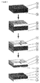
第1の実施形態において、ワークピース2は商業的に入手可能な単結晶シリコンウエハである。図1は、4工程(上部から下部へ)の本発明による代表的なプロセス順序を斜視図において図式的に示す。以下の参照において、符号は図1に関するものである。
In the first embodiment, the
工程1:ここでの基本的原材料は、例えばマイクロエレクトロニクスまたは太陽光発電産業において使用されるので、チョクラルスキー法に従って生産された単結晶シリコンウエハ2である。ウエハ2は、約76mmの直径および約0.4mmの厚みを有する。ウエハは軽くnドープまたはpドープされ、約10オームcmの特異的電気抵抗率を有し、その2つの表面1aおよび1bは<100>結晶面に平行に配向される。ウエハの1つまたは両方の表面1aおよび/または1bは、鏡面研磨または単純にエッチングしてラップすることができる。ウエハ2はウエハ生産からそのまま使用することができるか、またはそれは従来の方法を使用して(例えば有機溶媒および水でまたはプラズマ酸化洗浄によって)荒く予備洗浄することができる。
Step 1: The basic raw material here is a single
工程2:ウエハ2aの各表面1aおよび1b上に、ポリジオルガノシロキサン(例えばポリジメチルシロキサン(またはPDMS);続く考察では便宜上PDMSを指すが、任意の好適なシリコーン重合体または共重合体を使用できることを理解すべきである)の薄層3a、3bを適用し硬化させる(または硬化を可能にする)。これらの補助層3a、3bの好ましい厚みは0.01mm〜10mmの間であり、約0.3mm〜約3mmの間の厚みがより好ましい。2つの層3a、3bの厚みはこの例示的な実施形態において同じであるが、他の実施形態において2つの層の厚みは異なってもよい。PDMSについては、例えばDow Corning社によるSYLGARD 184を、硬化剤と基部材との間の1:10の混合比で、使用することが可能である。液体のPDMS混合物を最初に真空中で約1時間脱気し、次いでそれを所望される厚みでウエハ2の各表面1a、1b上に適用し、ホットプレート上で硬化させる(例えば100℃で30分間)。この例示的な実施形態において、PDMS層3a、3bは大部分のウエハ領域にわたって均質の厚みを有する。これは、水平表面上にウエハを置くこと、およびそれを硬化させる前に重力によってPDMSを平衡化させることによって達成することができる。PDMSを硬化させた後に、3層の複合物(PDMS 3a−ウエハ2−PDMS 3b)を室温まで冷却する。その後に、ウエハ2の縁部にPDMSが本質的にはなく、PDMSがウエハ2の2つの表面1a、1bのみを覆うように、ウエハ2の周面に沿って突出するPDMSを鋭いナイフで除去する。任意のPDMSをウエハ表面にPDMSを慎重に適用し水平表面上にそれを平衡化させることによって、ウエハの周面を超えて突出させない(およびしたがってウエハの縁部に接触する)ようにすることが可能であり、このような手段で、PDMSの表面張力はそれがウエハ縁部へオーバーフローしないようにする。
Step 2: On each
工程3:次いでパターン形成工程を実行する。鋭いナイフまたはカミソリ刃等のツールを使用して、PDMS層3aの1つの表面に任意パターンの線6および/または他の幾何学的図形(円等)を切断する。この実施形態において、すべての切断はPDMS層3aへ同じ深さを有し、PDMS層3aの厚みよりも少ない(すなわち、PDMS層3aは、ウエハ表面1aを通してどこにも完全に切断されない)。例えば好ましい厚みが1mmのPDMS層3aについては、これらの切断については好ましい深さは0.01mm〜0.99mm、より好ましくは0.1mm〜0.9mmの範囲である。
Step 3: Next, a pattern forming step is performed. A tool such as a sharp knife or razor blade is used to cut an arbitrary pattern of lines 6 and / or other geometric shapes (such as circles) on one surface of the
工程4:パターン形成工程後に、複合物(PDMS 3a−ウエハ2−PDMS(3b))を、液体窒素浴(温度、約−200℃)中に完全に浸漬する。シリコン(約3*10-6K-1)およびPDMS(約300*10-6K-1)の大きく異なる熱膨張率のために、この冷却によって複合物中に大きな機械的応力が誘起される。しかしながら、PDMS層3aが切断されたパターン6の一部の領域において、機械的応力は切断の構成および深さに依存して局所的に異なる。冷却の数秒後に、ウエハ2は、その表面1aに平行に、2つの薄い単結晶シリコンディスク5へと自然に割裂し、各ディスク5の1つの側面は、対応するPDMS補助層3aまたは3bがまだ接着されている。
Step 4: After the pattern formation step, the composite (
適切な配慮をすれば、2つのシリコンディスク5の各々は1つの単一ピースから本質的にはなり、割裂が起こる表面を持ち、その表面4上のパターン6のイメージ7aまたは7bを示す。2つのシリコンディスク5上のイメージパターン7aおよび7bは、実質的に相補的である。イメージパターン7aおよび7bの各々におけるフィーチャは、周囲の領域と比較して、異なる表面の粗度の領域、異なる表面の高さ(すなわち対応するシリコンディスク5の異なる局所的な厚み)、または表面性質の他の差を含むことができる。パターン6の横の特徴は、同じスケールで、相補的なイメージ7aおよび7bで実質的に再現される。約0.1mmを超える横寸法を有するパターン6中のフィーチャは、イメージパターン7aおよび7bで複製することができる。表面4に垂直な追加の破損を回避するために、ディスク5は、割裂後に、全PDMS補助層が少なくとも室温まで再び加温されるまで、100℃のホットプレート上に(PDMS補助層3aまたは3bが接着された側面を下に面して)液体窒素浴から直接移動させることができる。どんな加温手順が用いられても、ディスク5は、加温されるにつれて、層のカーリングを戻すように平らな支持に対して慎重にプレスして加温が進行するにつれて層を平らにすることは好ましい。
With proper care, each of the two
この方法に従って生産された表面パターン7aおよび7bを備えた薄シリコンディスク5は、オリジナルのウエハ2と同じ特性を備えた単結晶シリコンから実質的になり、直接使用することができる。あるいは、PDMS補助層3aまたは3bは、例えば適切な液体エッチング液(例えばNMP(N−メチルピロリドン)およびTBAF/THF(テトラブチルフッ化アンモニウムのテトラヒドロフラン中の1.0M溶液)の容積で3:1の混合物)中での浸漬によって、またはフッ化水素酸中の浸漬によっても、シリコンディスク5から除去することもできる。PDMS補助層3aまたは3bを除去するための好ましい手段は、好ましくは150℃より上の(より好ましくは200℃より上の)温度の熱硫酸(H2SO4)エッチング液によりリンスすることまたは熱硫酸浴中で浸漬すること、次いで生産された白色シリカフォームを機械的に(例えばブラシおよび場合によっては複数のブラッシング−エッチングサイクルを使用して)除去すること、および最終的にフッ化水素酸中での浸漬によってシリコンディスク5を洗浄することである。
The
第2の例示的な実施形態において、パターン形成工程(工程3)は、鋭いナイフによる切断する代わりにレーザー光線による照射を使用して実行される。レーザーは、好ましくはPDMSによって強く吸収される周波数を有し(炭酸ガスレーザーはこの基準を満たす)、好ましくはPDMS層3aに対する光線の強度および動きは自動様式または手動様式で制御されて、所望されるパターンを切断する。商業的に入手可能なレーザー光線切断機(例えば60ワットの炭酸ガスレーザーを備えたVERSA LASER VLS 6.60)が許容される。切断の深さは、個別にまたは組み合わせで使用することができる複数の手段のいずれかでも変更することができ、すなわちレーザー光線は異なる深さで焦点を結ぶことができ、レーザー強度は変更することができ、PDMSの表面3aに対するレーザー光線の走査速度は変更することができ、レーザーのパルス率は変化させることができ、レーザー光線はPDMSの表面の3a上の同じスポットに対して繰り返し通過させることができる(場合によっては通過の間の表面洗浄工程と共に)。
In a second exemplary embodiment, the patterning step (step 3) is performed using irradiation with a laser beam instead of cutting with a sharp knife. The laser preferably has a frequency that is strongly absorbed by PDMS (a carbon dioxide laser meets this criterion), and preferably the intensity and movement of the light with respect to the
第3の実施形態において、パターン形成工程は、鋭いナイフにより切断する代わりに化学エッチングを使用して、場合によってはPDMSの表面にマスク層を使用して、および場合によってはナイフまたはレーザー切断と組み合わせて、実行される。 In a third embodiment, the patterning process uses chemical etching instead of cutting with a sharp knife, optionally using a mask layer on the surface of PDMS, and optionally combined with knife or laser cutting. And executed.
第4の実施形態において、パターン形成工程は選択された位置でPDMS表面3aを局所的に焼くことによって実行されるが、レーザー光線を使用する代わりに、所望されるパターンのエンボス形状を示すホットスタンプをPDMS表面3a上にプレスする。ホットスタンプは好ましくはPDMS分解温度より上の、より好ましくは550℃より上の温度である。
In the fourth embodiment, the patterning process is performed by locally baking the
第5の実施形態において、パターン形成工程は、以前に言及されたもの等の様々な可能な切断メカニズムのいずれかを使用して実行される。このケースにおいて、しかしながら、線がPDMSの表面の3aへと切断されるだけではなく、横に延長され、PDMSの表面の3aへと課されるディスク等の2次元フィーチャとなる。これは、スキャナーの様式で発射するレーザーの制御に使用されるイメージデータに基づいたフィーチャを生成するために、例えばレーザーをラスタ様式で使用することによって行うことができる。
In a fifth embodiment, the patterning process is performed using any of a variety of possible cutting mechanisms such as those previously mentioned. In this case, however, the lines are not only cut to 3a on the surface of the PDMS, but are also extended laterally, resulting in a two-dimensional feature such as a disc that is imposed on the
第6の実施形態において、本方法のパターン形成工程は、前述のもの等の様々な切断メカニズムのいずれかを使用して実行される。しかしながら、本明細書において、切断の深さはパターン6の全体にわたって一定に保たれないが、所定の手段で局所的に変更される。言いかえれば、パターン6のフィーチャは異なる深さで与えられ得る。このような手段で、例えば、局所的に異なる高さを備えたフィーチャはイメージパターン7aおよび7bにおいて生産することができる。極端な例において、切断は、ウエハ2の表面1a上にPDMS層3aを介して最後まで実行することができる。これを、例えば満たされた円(すなわちディスク)からなるパターン6に対して行うならば、2つの生産されたディスク5のうちの1つは、貫通孔のイメージパターン7aを有し、他の1つは、オリジナルのウエハ2と同じ厚みを備えた形作られたメサの対応する相補的パターン7bを有する。
In a sixth embodiment, the patterning step of the method is performed using any of a variety of cutting mechanisms such as those described above. However, in this specification, the cutting depth is not kept constant throughout the pattern 6, but is locally changed by a predetermined means. In other words, the features of pattern 6 can be given at different depths. By such means, for example, features with locally different heights can be produced in the
第7の実施形態において、パターン形成工程は、PDMS補助層3aへとパターンを切断することによってではなく、所望されるパターンのフィーチャに対応する特定の位置でPDMS層3aの特性を局所的に修飾することによって実行される。例えばPDMSの機械的特性、および特に、そのCTEは、以下技法[Huck et al., Langmuir (2000), 16:3497-3501]を使用して局所的に修飾することができる。PDMS層3aはジクロロメタン中の0.25Mのベンゾフェノンの溶液中で5時間浸漬される。次いで、PDMS層3aを大気中で暗闇で24時間乾燥する。ベンゾフェノン(光増感剤)が照射に際してラジカルを生成するので、この処理は紫外線(UV)光による照射に対するPDMSの感度を増加させ、これらのラジカルはPDMSを架橋する。次いで、PDMS層3aは所望されるパターン6を示す幅のフォトマスクを介してUV照射(例えば254nm、10〜30分)に露光される。PDMS層3aの露光領域は、より剛性かつよりエラストマー性でなくなり、周囲の領域のものとは異なるCTEおよび弾性率を有する。マスクによってパターン形成した紫外線で感光性のあるPDMSを照射する代わりに、感光性のあるPDMSは、その代りに、例えばUVレーザーを使用して露光することができる。さらに、所望されるパターンのフィーチャに対応する位置でのPDMSの選択的に促進された架橋(それはそのCTEおよび局所的な応力生成に影響を及ぼし得る他の機械的特性を局所的に修飾する)は、例えばPDMS層3aの表面上の特定のパターンを選択的に加熱する赤外線レーザーによる照射を介して、焼かずに、達成することができる。
In the seventh embodiment, the patterning process locally modifies the characteristics of the
第8の実施形態において、パターン形成工程は、PDMS補助層3aへとパターンを切断することによってではなく、所望されるパターンのフィーチャに対応する位置でPDMS層3aの特性を局所的に修飾することによって実行される。例えばPDMSの機械的特性、ならびに特にそのCTEおよび/またはその弾性率は、PDMS層へと異なる特性(異なるCTEおよび/または異なる弾性率等)を備えた他の材料(ガラスビーズ、気泡、金属粒子、ファイバー等の)を、局所的に組み込むことによって局所的に修飾することができる。
In the eighth embodiment, the patterning step locally modifies the characteristics of the
第9の実施形態において、パターン形成工程は、少なくとも1つのパターン形成層、および異なる材料(および場合によっては異なる特性(異なるCTE等)を備えた)から、場合によっては作製される少なくとも別の非パターン形成層を含む不均一な補助層3aの使用によって実行される。1つの実装において、PDMSを適用する前に、パターン6の金属構造は、例えばスクリーン印刷技法またはリソグラフィーおよび物理蒸着法を使用して、ウエハ2の表面上に被着される。次いでPDMSをこの金属構造およびウエハの両方に対して適用し(その結果として部分的に金属構造を組み込み)、次いで硬化させる。金属構造の特性(CTE等)はPDMSの特性とは異なるので、生産された薄ディスク5は実質的にパターン6の金属構造のイメージである表面構造パターン7aおよび7bを有する。
In a ninth embodiment, the patterning step comprises at least one other layer that is optionally made from at least one patterning layer and different materials (and possibly different properties (such as different CTEs)). This is done by the use of a non-uniform
第10の実施形態において、本方法を使用して、ウエハ2を2つの薄ディスク5へと割裂させ、使用されるパターン6は鏡面対称なパターンである。これは、実質的に同一のイメージパターン7aおよび7bを有する2つの薄ディスク5を生産する。すなわち、2つの同一の製品(「デバイス」)は「1工程で」(すなわち、本方法のただ1回の適用を使用して)生産することができる。PDMS補助層3aおよび3bの特性(例えばそれらの厚み)は、2つの生産された薄ディスク5の厚みが同じであるかまたは互いに異なるように選択することができる。
In the tenth embodiment, using this method, the
第11の実施形態において、本方法は、ウエハの1つの側面上のPDMS層3aにおける特定のパターン6、およびウエハの他の側面上のPDMS層3bにおける別のパターン’6と共に使用される。パターン’6はパターン6と同じかまたは異なるパターンであり得る。この実施形態に記載の方法によって生産される、薄ディスク5上のイメージパターン7aおよび7bは、実質的にパターン’6および6の組み合わせ(例えば重ね合せ)である。
In the eleventh embodiment, the method is used with a specific pattern 6 in the
第12の実施形態において、本方法は、PDMS層3aにおける特定のパターン6および/またはPDMS層3bにおけるパターン’6を最初に使用して、2つの薄ディスク5(1つは対応するイメージパターン7aおよび他のものは1つの側面上の対応する鏡面イメージパターン7bを有する)を生産する。2枚のディスク5の各々は他の側面上にPDMS層3aまたは3bが通常まだ接着されている。次いで、これらの層は新たなPDMS層と置換することができるが、これらの層3aおよび3bをそれぞれのディスク5に接着させておくことが好ましい。それらが置換されるか再び使用されるかにかかわらず、次いで、これらの層3aおよび/または3bは所望されるならばパターン形成することができるか、またはそれらが方法の第1の反復の間に既にパターン形成されならば(パターン6または6’により)、それらのパターンは修飾することができる(すなわち2つの薄ディスク5の生産のために)。次いで、方法は、まだPDMS層が接着されていない2つの薄ディスク5のそれらの側面(すなわち表面構造パターン7aまたは7bを有する側面)上に次の反復のための新しいPDMS補助層を被着することによって再び適用される。これらの新しいPDMS補助層のうち、0、1または2つは、所望されるならば(任意の所望されるパターンにより)パターン形成することができる。次いで、方法の第2の反復により合計4つのより薄いディスクが生産され、それらの4つのうち2つのより薄ディスク(一般に)は、両側面上に局所的に制御可能なパターンの表面構造を有する(すなわち両側印刷に同等である)。1つの側面上に、第1の反復の間に古いPDMS補助層3aおよび3bにおけるパターン’6および6の重ね合せに対応するイメージパターン7a(またはそれぞれその鏡面イメージ7b)を有し、および他の側面上に、古いPDMS補助層3a(または3b)における任意の(場合によっては修飾された)パターンの重ね合せに対応するイメージパターンおよび対応する新しいPDMS補助層における任意のパターンを有する。このような手段で、両側面上に類似または異なる構造化表面を備えた固体状材料の薄い独立層を生産することができる(この実施形態による方法は、1つの側面上のみに表面構造(第2の反復からのイメージパターンに対応する)を有する2つの他のより薄ディスクも同時に生産する)。第1の反復の間に生産された薄ディスク5上の表面構造が、第2の反復の間の応力パターンおよびしたがって生産された表面構造になんらかの影響を及ぼし得るが、この影響は通常小さく(通常生産された表面構造の厚みがディスクの厚みよりもはるかに小さいので)、補助層の適切なパターン形成を第2の反復について使用して償うことができることに注目されたい。
In the twelfth embodiment, the method first uses two specific thin discs 5 (one
第13の実施形態において、PDMS層3aにおいて局所的に異なるCTEを備えたパターン6の領域を有しており、温度変化に対して複合物構造をさらす代わりに、PDMS層3aにおいて局所的に異なる応力(すなわち応力パターン)を誘起する他のメカニズムを使用することも可能である。例えば、同じ温度変化を全PDMS補助層のために使用する代わりに、例えば補助層における特定の領域を他の領域よりも強く選択的に冷却することによって(例えば所望されるパターン6を有する冷却エンボススタンプとの接触を使用して)、または全層の冷却および特定の領域の例えばレーザーによる選択的再加熱によって、PDMS補助層における異なる位置で異なる温度変化を課すことができる。このような手段で、均質のPDMS補助層を使用して、局所的に異なる応力のパターンをもたらすことが可能である(この実施形態については、PDMS等の比較的低い熱伝導率を備えた補助層材料を使用することが好ましい)。より一般的には、局所的に規定可能な応力パターンは、例えば光パターン、熱パターン(異なる温度を有する異なる領域)、溶媒パターン(異なる溶媒濃度を有する異なる領域)、電場または磁場のパターン、補助層上に作用する外部の機械力のパターン等の、パターン6の局所的に変動し外部から適用される物理的または化学的条件(それはさらに一時的に変化し得る)に対して補助層をさらすことによって、生産することができる。補助層は、その容積を(局所的に)変化させることによって、外部から適用される物理的条件または化学的条件のこれらのパターン6と相互作用する少なくとも1つの材料を好ましくは含む(例えば紫外線の下でまたは電場/磁場等において膨張する材料)。
In the thirteenth embodiment, the
第14の実施形態において、局所的に異なる応力のパターンを誘起するための別の代替方法は、PDMS層3aにおける特定の位置で圧電アクチュエータ等のアクティブデバイスを含み、それら(例えば、電気的に光学的に)を動作させてPDMS層3aにおける応力パターンを生成することである。より一般的には、局所的に規定可能な応力パターンは、化学的または物理的メカニズムによって活性化された場合に異なる体積変化をするパターン6の異なる材料をPDMS層3aの中へ組み込むことによって生産することができる。かかる体積変化を達成することができるメカニズムは、温度変化に加えて、湿度の変化(例えば膨潤、脱水和)、溶媒組成物および/またはイオン強度の変化(例えば浸透圧アクチュエータ、多価電解質ゲル、イオン性重合体金属複合物、導電性重合体、カーボンナノチューブアクチュエータ)、pH変化、相変化(例えば組み込まれた溶媒の凍結)、化学反応(例えば重合体ゲル)、電気的活性化(例えば圧電材料または電歪材料、静電アクチュエータ、電気活性重合体)、磁気活性化(例えば「磁性」ゲル)、光学的活性化(例えば液晶エラストマー、 光反応性材料)等と同様に、これらのいずれかまたはすべての組み合わせを含む。さらに、PDMS層3aの中へ異なる材料のパターンを局所的に組み込む代わりに、例えば重合体に対して異なる機能的側鎖を局所的に加えることまたは例えばUV照射によって架橋度を局所的に変化させることによって、所望される局所的に異なる容積変化挙動を達成するために、(化学的に)PDMS自体を局所的に修飾することは可能である。
In the fourteenth embodiment, another alternative method for inducing locally different stress patterns includes active devices, such as piezoelectric actuators, at specific locations in the
第15の実施形態において、工程4における割裂の開始は促進され、割裂プロセスの制御は、ウエハ表面上の特定の特異的位置で1つまたは複数の構造的により脆弱な域を備えたウエハ2の提供によって改善される。例えば、1つまたは複数の小さな欠損域は、ウエハ2の縁部で作成することができる。かかる欠損域は、機械的に(例えば、鋭いとがったハンマーによりウエハ縁部上の特定のスポットを叩き、その結果として結晶構造を局所的に粉砕し、くぼみまたはニックを生成することによって、または溝または刻み目を生成するために鋸切断、鑢仕上げ、または磨砕等によって)、化学的に(例えば局所的な溝のエッチング)、光学的に(例えばレーザーを使用して材料を局所的に溶融すること、または材料を融解除去して溝構造の作成すること)、または他の好適なメカニズムによって、作成することができる。次いで、割裂はそれらの欠損域で優先的に開始され、ウエハ領域の残りに対してそこから伝播する。特に、これらの欠損域の位置の変動によって、割裂の最初の深さ(すなわちそれらの縁部での生産された薄ディスク5の厚み)をよりよく制御し、ディスク5の縁部の質を一般に改善することが可能であるので、これは遊離である。例えば、2つの表面1aおよび1bの間の中間のウエハ2の縁部における溝(すなわち周面付近の)は、等しい厚みの2つの薄ディスク5へと明確な縁部を備えて割裂を促進することができる。応力がワークピースにおいて誘起される前に(例えば冷却前に)、この実施形態に従ってより脆弱な域が作成されるか、またはウエハが既に応力下にある状態でより脆弱な域が生成され得る。第2の方法は、割裂が開始する瞬間をよりよく制御することも可能にする。割裂プロセスが自然に始まる、応力が臨界値よりちょうどわずかに下の大きさまでウエハにおいて確立されれば、次いで脆弱さが生成されるとすぐに、割裂はその脆弱位置から優先的に開始される。
In the fifteenth embodiment, the initiation of splitting in
第16の実施形態において、ウエハを単純に自然に割裂させる代わりに、工程4における割裂の開始は、制御された衝撃(例えば短い衝撃波)に対してウエハ2をさらすことによって促進される。例えば、ウエハにおける衝撃波は、ハンマー(ピーニング)等のメカニカルデバイスによる1つまたは複数の制御された打撃によって、超音波パルスの提供によって、または強いレーザーパルスによって等で、誘起することができるかかる衝撃波の空間分布、強度および時間的特徴は、修飾を促進し、割裂プロセスをよりよく制御する。
In the sixteenth embodiment, instead of simply splitting the wafer naturally, the initiation of splitting in
第17の実施形態において、本方法は、2つの表面1aまたは1bの少なくとも1つの上に既存の表面構造を既に有するウエハ2上で使用される。かかる既存の表面構造(トレンチ、メサ、膜、カンチレバー、ピラミッド等)は、ウエハ材料それ自体から形成することができるか、またはそれらは追加材料(例えば金属接触、反射防止層、誘電体層、エピタキシャル層等)、またはその任意の組み合わせを含むことができる。次いでPDMSを既存の構造に対して適用し、それらを覆い等角的に囲んで、PDMSの硬化後に、既存の構造をPDMS層3aおよび/または3b中に部分的に組み込まれるようにする。ウエハ2が2つの薄ディスク5へと割裂する場合、既存の表面構造は、対応するPDMS補助層3aまたは3bがまだそれに接着される各ディスク5の側面上に維持されているが、各ディスク5の他の側面はパターン6のイメージとして本方法によって生成された新しい表面構造7aまたは7bを示す。このような手段で、1つの側面上に複雑な表面構造(場合によっては追加材料も含み、電子デバイス、光学デバイス、化学デバイスまたはマイクロメカニカルデバイス等の完全に機能的なデバイスをも提供する)、他の側面上に他の表面構造(そこでそれらの他の表面構造はウエハ材料から形成され、PDMS層におけるパターン6によって決定される)を備えた薄い独立層を、生産することができる。表面1aおよび/または1b上の既存の表面構造が、応力パターンおよびしたがって生産された表面構造7aおよび7bになんらかの影響を及ぼし得るが、この影響は多くの場合小さく(既存の表面構造の厚みが多くの場合ディスクの厚みよりもはるかに小さいので)、補助層3aおよび/または3bの適切なパターン形成を使用して償うこともできることに注目されたい。
In a seventeenth embodiment, the method is used on a
第18の実施形態において、本方法は、例えば1つまたは複数のドーパント勾配等の既存の内部(バルク)構造を既に有するウエハ2上で使用される。ウエハ2が2つの薄ディスク5へと割裂する場合、既存の内部構造は対応する薄ディスク5中に維持される。このような手段で、ドーパント勾配等の内部(バルク)構造を有する、構造化表面を備えた薄独立層は生産することができる。
In an eighteenth embodiment, the method is used on a
第19の実施形態において、先の2つの実施形態からの態様を組み合わせて、本方法は、既存の表面構造および既存の内部(バルク)構造の両方を既に有するウエハ2上で使用される。特に、ウエハは、その表面1aおよび/または1bの1つまたは両方上に機能的なデバイス(電子デバイス、光学デバイス、マイクロメカニカルデバイス、化学デバイス等)を部分的にまたは完全に有している。かかるデバイスは、LED、レーザーダイオード、太陽電池、タンデム太陽電池、電力増幅器、集積回路一般、センサまたはアクチュエータ等のマイクロエレクトロメカニカルデバイス等を含むことができる。次いでPDMSをウエハ表面上の既存のデバイスに対して適用し、デバイスを覆い、外側で等角的にそれらを囲んで、PDMSの硬化後に、既存のデバイスをPDMS層3aおよび/または3b中に部分的に組み込まれるようにする。ウエハ2が2つの薄ディスク5へと割裂する場合、既存のデバイスは、対応するPDMS補助層3aまたは3bのそれぞれがまだ接着される各ディスク5の側面上に維持されるが、各ディスク5の他の側面はパターン6のイメージとして生成された新しい表面構造7aまたは7bを示す。このような手段で、1つの側面上に複雑で、部分的にまたは既に完全に機能的なデバイス、および他の側面上に他の表面構造(そこでそれらの他の表面構造はウエハ材料から形成され、PDMS層におけるパターン6によって決定される)を有する、固体状材料の薄い独立層を生産することができる。
In a nineteenth embodiment, combining the aspects from the previous two embodiments, the method is used on a
先の実施形態の適用のための例示的な例として、従来のシリコン太陽電池(例えばpn接合、前方の金属接触グリッド、抗反射コーティングを含む前側ドープ層)の前方部(すなわち正常操作の間に照射される側面)を構築する表面構造および内部構造が考慮され、以下において「前部構造」と称される。ここで、ウエハの1つの側面上にのみこれらの「前部構造」を従来通りに生産する代わりに、かかる「前部構造」は、厚い単結晶シリコンウエハ2の両側面1aおよび1b上に製造される。次いでこのウエハ2は上記されるような2つの薄ディスク5へと割裂し、それによってデバイス層は維持されて、ここでこれらの2つのディスク5の各々は「前部構造」を有するが、1つの側面(すなわち、対応するPDMS層3aまたは3bがまだ接着される側面)上でのみ有するようにする。2つのディスク5の各々の他の側面上に、PDMSにおけるパターン6によって決定された表面構造7aまたは7bを備えた、バルクウエハ材料からなる「新たな」表面がある。両方のディスクの「新たな」表面は、シリコン太陽電池の裏側の作製のために従来の方法を使用してさらに加工することができ(例えば裏面電界ドーピングおよび裏側接触金属化等)、2つのシリコン太陽電池の製造が完了する。この実施例は以下の多数の利点を示す。大部分の太陽電池製造工程は、比較的厚い(およびそれゆえ脆弱でない)ウエハ2上で行うことができ、それは接触スクリーン印刷等の低費用のプロセスの使用を促進し、一般に扱われるウエハを単純化する。さらに、同じ(前側)ドーパントは、ウエハの全表面へと(すなわちその側面1aおよび1bの両方へと)拡散させることができ、例えばウエハの裏からドーパントを続いて除去する必要はない(それが割裂プロセスによって自動的に達成されるので)。同じことは例えば反射防止コーティングの場合にも言え、それは全ウエハ上で生産することもでき(例えばSiO2の酸化成長および/またはSi3N4窒化物のPECVD被着)、次いで割裂プロセスを介して1つの側面に自動的に制限される。このような手段で、太陽電池製造のための多数の加工工程は、本方法の適用によって排除または単純化することができる。前部および背部の接触を備えた標準的な太陽電池の代わりに裏面接触太陽電池が製造される場合、これらの利益は別の例示的な例において特に著しい。本明細書において、機能的構造のほとんどすべては電池の1つの側面(裏側)上にある。かかる裏側構造が厚い単結晶シリコンウエハ2の両方の表面1aおよび1b上に製造されるならば、本方法を使用した割裂後の、生産された薄ディスク5の両方は既にほとんど完成した裏面接触電池である(恐らく他の側面上に反射防止コーティングの被着のみを必要とする)。それゆえ、プロセスの大部分を介して薄ウエハを扱う必要なしに、薄い単結晶シリコン裏面接触太陽電池を生産することに、本方法を適用することができる。
As an illustrative example for the application of the previous embodiments, the front portion (ie during normal operation) of a conventional silicon solar cell (eg, pn junction, front metal contact grid, front doped layer including anti-reflective coating). The surface structure and internal structure that make up the illuminated side) are considered and will be referred to below as the “front structure”. Here, instead of producing these “front structures” conventionally only on one side of the wafer, such “front structures” are produced on both side faces 1 a and 1 b of the thick single
別の態様において、本発明は、2ピース(1ピースは他のピースの幾何学的な相補物である)へとギャップによって分割した固体状材料のスラブ(ブロック、インゴット、ディスク等)を含み、ギャップをゼロまで減少させることによって、実質的に欠損した材料なしで(例えば内部空隙等なしで)、オリジナルのスラブの形状、寸法および重量を取り戻すことができるようにしたデバイスに関する。それらの2ピースの少なくとも1つは、薄層(すなわち、実質的に水平または湾曲した少なくとも1cm2の領域を有し、その厚みがこの領域の全体にわたって2mm未満、好ましくは0.5mm未満であるシート)である。薄層ピースの少なくとも1つのそれ自体は、ギャップの反対の表面上で、少なくとも1つの追加の固体状材料(補助層と称される)の層をそれに接着する。2ピースの各々については、ギャップに面する表面は、スラブのバルクにおいて見出されるもの以外の材料を含有しない。(場合によっては、例えば表面が大気と反応性で大気に露出されるならば、天然の酸化層を除いて)。 In another aspect, the invention includes a slab (block, ingot, disk, etc.) of solid material divided by a gap into two pieces (one piece being the geometric complement of the other piece), It relates to a device that allows the shape, size and weight of the original slab to be regained by reducing the gap to zero without substantially missing material (eg, without internal voids, etc.). At least one of those two pieces has a thin layer (ie, a substantially horizontal or curved region of at least 1 cm 2 and a thickness of less than 2 mm, preferably less than 0.5 mm throughout this region. Sheet). At least one of the thin layer pieces itself adheres to it a layer of at least one additional solid material (referred to as an auxiliary layer) on the opposite surface of the gap. For each of the two pieces, the surface facing the gap contains no material other than that found in the bulk of the slab. (In some cases, for example, if the surface is reactive to the atmosphere and exposed to the atmosphere, except for the natural oxide layer).
別の実施形態において、本発明は上記されるようなデバイスに関するが、2ピースの各々については、ギャップに面する表面はあるパターンに従う構造(他のピース上の表面構造7bに実質的に相補的な1ピース上の表面構造7aを持ち、2ピースのうちの少なくとも1つに接着された実質的に少なくとも1つの追加の固体状材料(補助層)の少なくとも1つの層における対応パターン6のフルサイズのイメージであるパターンを持つ)を示すデバイスに関する。補助層におけるパターン6は、補助層の部分に周囲の領域の材料特性とは異なる局所的な材料特性(局所的に異なるCTEまたは局所的に異なる弾性率等)を示すようにすること(それは、例えば補助層の材料が部分的にまたは完全に除去される部分(すなわち空隙構造)を含むことができる)によって実現される。別の実施形態において、パターン6は、光パターン、熱パターン、補助層上に作用する外部の機械力のパターン等の外部の物理的影響または化学的影響のパターンの補助層上への適用によって、補助層において一時的に誘起される応力のパターンであり得る。
In another embodiment, the present invention relates to a device as described above, but for each of the two pieces, the surface facing the gap is a structure according to a pattern (substantially complementary to the surface structure 7b on the other piece). Full size of corresponding pattern 6 in at least one layer of substantially at least one additional solid material (auxiliary layer) having a
本発明のアプローチは、単結晶シリコン以外の固体状材料(例えば多結晶シリコン、サファイア、ゲルマニウム、石英またはガラス等の非晶質材料)からなるワークピースから、構造化表面を備えた薄独立層を生産するのに使用することができる。さらに、このアプローチは、複数の異なる材料(均質または非均質の複合物材料等)からなるワークピース、または内部構造(ラミネート等)を有するワークピースと共に使用することができる。例えば、このアプローチは、表面上に窒化ガリウム(GaN)等のエピタキシャルに成長した層を備えた単結晶シリコンウエハからなるワークピースのために使用することができる。さらに、ワークピース上に適用される補助層については、PDMS以外の材料(例えば、他のポリシロキサン(例えば電気活性のための有機金属基を含むことができる)、他のエラストマー、他の重合体もしくはプラスチック一般、またはアルミニウムもしくは銀等の金属など)を使用することができる。複数の異なる材料(均質または非均質の複合物材料等)からなる補助層、または内部構造(ラミネート等)を有する補助層を利用することも可能である。一般に、ワークピースは比較的脆弱な固体状材料である。ワークピースと補助層との間の優れた接着はプロセスの全体にわたって達成され維持されるべきであり、補助層は、補助層それ自体が破損されることなく十分に強い応力パターンを課するのに好都合なプロセスに従うべきである。 The approach of the present invention is to create a thin independent layer with a structured surface from a workpiece made of a solid material other than single crystal silicon (eg, amorphous material such as polycrystalline silicon, sapphire, germanium, quartz or glass). Can be used to produce. Furthermore, this approach can be used with workpieces made of a plurality of different materials (such as homogeneous or non-homogeneous composite materials), or workpieces having an internal structure (such as a laminate). For example, this approach can be used for workpieces consisting of single crystal silicon wafers with epitaxially grown layers such as gallium nitride (GaN) on the surface. In addition, for auxiliary layers applied on the workpiece, materials other than PDMS (eg other polysiloxanes (eg can contain organometallic groups for electroactivity), other elastomers, other polymers) Alternatively, plastic in general, or a metal such as aluminum or silver) can be used. It is also possible to use auxiliary layers made of a plurality of different materials (such as homogeneous or non-homogeneous composite materials) or auxiliary layers having an internal structure (such as a laminate). In general, the workpiece is a relatively fragile solid material. Excellent adhesion between the workpiece and the auxiliary layer should be achieved and maintained throughout the process, and the auxiliary layer imposes a sufficiently strong stress pattern without damaging the auxiliary layer itself. You should follow a convenient process.
さらに、補助層におけるPDMS(または他の重合体)は、ホットプレート上での加熱以外の手段によって硬化(すなわちその重合体鎖の架橋)させることができる。例えば、その上に高温ガスを送風すること、または例えば赤外光により照射することによって加熱することができる。あるいはまたは加えて、硬化は、化学添加剤、紫外線または電子線を使用して遂行することができる。PDMS(もしくは他の重合体、または一般に補助層における任意の材料)を化学的に修飾して、硬化の特定の形態(または一般に凝固、場合によっては凝固の間に既に層の内側に内部応力を生成する)を促進することができ、例えば、UV照射によるPDMSの硬化は、例えばベンゾフェノン(照射下でラジカルを生成する光増感剤)中のPDMSの浸漬によって、または例えばPDMS中のメチル基を光反応性の置換基と置換することによって促進することができる。 Further, the PDMS (or other polymer) in the auxiliary layer can be cured (ie, the polymer chains cross-linked) by means other than heating on a hot plate. For example, it can be heated by blowing hot gas over it, or by irradiating it with infrared light, for example. Alternatively or additionally, curing can be accomplished using chemical additives, ultraviolet light or electron beams. PDMS (or other polymer, or generally any material in the auxiliary layer) can be chemically modified to create a specific form of cure (or generally solidification, and possibly internal stress inside the layer already during solidification). For example, curing of PDMS by UV irradiation, for example, by immersion of PDMS in benzophenone (a photosensitizer that generates radicals under irradiation) or, for example, methyl groups in PDMS This can be facilitated by substitution with photoreactive substituents.
同様に、多数の代替方法を使用してプロセスの終了時にディスク5から補助層を除去することができる。上記されるような補助層を化学的エッチングで除去する代わりに、またはそれに加えて、この層は、照射、電子線、および/または熱によって、機械的に除去することができる。例えば、PDMS層の反対のディスクの表面を一時的に支持に固定する(例えば固着する)ならば、単結晶シリコンの薄ディスク5からPDMS補助層を機械的に剥離することができ、例えば次いで角から開始してPDMSをディスクの表面に対して実質的に垂直な方向で引っ張ることによって、場合によっては PDMS層およびディスク5の間でくさびまたは類似のアイテムを挿入することによって促進して、ゆっくり慎重に剥離する。あるいは、PDMS(または他の重合体)を、その分解温度より上に、例えばレーザーにより、またはオーブン中で単純に加熱することができる(すなわち灰化による除去)。それはプラズマ中の(例えば酸素プラズマ中で)灰化によっても除去することができる。PDMSが例えばUV照射の下で容易に分解するように化学的に修飾することもできる。最終的に、これらのアプローチのいずれかまたはすべてを組み合わせることができる(PDMS以外の材料が補助層のために使用されるならば、直接に適合される)。本アプローチは、ほとんど任意の形状のワークピースに適用することができ、平面のウエハに限定されていない。特に、本発明を使用して、例えば1つの側面上で平らにされた単結晶シリコンインゴットから構造化表面を備えた薄シートを直接剥離することができる。平らなシートを剥離するには、使用されるワークピースが少なくとも1つの平らな表面によって制限されることで十分である。次いでこの表面上に補助層を適用する。1つのシートのみを剥離することが可能であるか、またはワークピースの異なる表面から複数のシートを同時に剥離することが可能である。最終的に、本アプローチは構造化表面を備えた、薄く独立した湾曲したシートまたはシェルの生産にも適用することができる。この目的のために、補助層はワークピースの対応して湾曲した表面上に適用される。次いで、温度変化(または他の応力を誘起するプロセス)は、ワークピースの内側でパターン形成された破壊域に沿って、ワークピースの残りからの薄く対応して湾曲したシートまたはシェルの割裂をもたらす。このパターン形成された破壊域は、ワークピースと補助層との間の界面におよそ同じ距離で至る所に広がり、その結果表面構造パターンを備えた生産されたシートはおよそ均一の厚みを有する(厚み変異が故意に生産されてもよいパターン7aおよび7bを除いて)。
Similarly, a number of alternative methods can be used to remove the auxiliary layer from the
補助層が適用される表面の表面性質は重要ではない。界面は滑らかに研磨することができるか、または著しい粗度を有することができる。補助層に対する適切な接着を保持することのみが重要である。特に、破壊面(ワークピースからのシートから剥離する場合にワークピースの残りの上で形成される)は、補助層が適用される表面として続いて使用することができる。したがって、本アプローチは、ワークピースの残り上で再び適用することができる。このような手段で、単一ワークピースから、シートの後にまたシートを連続的に剥離することができる。 The surface properties of the surface to which the auxiliary layer is applied are not critical. The interface can be polished smoothly or have a significant roughness. It is only important to maintain proper adhesion to the auxiliary layer. In particular, the fracture surface (formed on the rest of the workpiece when peeling from the sheet from the workpiece) can subsequently be used as the surface to which the auxiliary layer is applied. Thus, this approach can be reapplied on the rest of the workpiece. By such means, the sheet can be peeled continuously from the single workpiece after the sheet.
さらに、構造化表面を備えた剥離された薄い独立層から、同じ工程の反復によって、(より薄い)層をさらに剥離することができる。例えば、本方法を使用して、単結晶シリコンウエハは、両側面上にPDMS補助層を適用することによって構造化表面を備えた2枚のディスクへと割裂させることができ;これらの補助層の1つまたは両方はどちらもパターン6を有することができず、両方がパターンを有するならば、これらのパターンは同じまたは互いとは異なることができる。次いで生産された2つのより薄いディスクの各々を、再びPDMS補助層を備えた両側上に提供することができ、再びそれらのうちの1つまたは両方はどちらも同じまたは異なり得るパターン(6)を有することはなく、この方法の工程を反復して、したがって構造化表面(所望されるならば異なる表面構造パターンを有する)を備えた2つのなおより薄いディスクへとさらに割裂させること等が可能である。このような手段で、構造化表面を備えた非常に多数の薄い単結晶ディスクは単一単結晶シリコンウエハから得ることができる。例えば、3工程で、カスタム構造化表面を備えた約50μm厚の8つのディスクを、従来の0.4mm厚のウエハから得ることができる。 Further, the (thinner) layer can be further peeled from the peeled thin independent layer with the structured surface by repeating the same process. For example, using this method, a single crystal silicon wafer can be split into two disks with structured surfaces by applying PDMS auxiliary layers on both sides; Neither one or both can have pattern 6, and if both have patterns, these patterns can be the same or different from each other. Each of the two thinner discs produced can then be provided again on both sides with a PDMS auxiliary layer, again one or both of which can have the same or different pattern (6) It is possible to repeat the steps of this method, thus further splitting into two even thinner disks with structured surfaces (with different surface structure patterns if desired), etc. is there. In this way, a large number of thin single crystal disks with structured surfaces can be obtained from a single single crystal silicon wafer. For example, in three steps, eight disks approximately 50 μm thick with a custom structured surface can be obtained from a conventional 0.4 mm thick wafer.
一般に、このように生産された薄い独立層の寸法、特に、それらの厚みは、応力を誘起するメカニズム(例えば温度変化)および/または補助層の特性の適切な選択を介して定めることができる。これは、応力誘導のタイムフロー、誘起された応力の大きさ、補助層の寸法、補助層の幾何学的形状、ならびに/または機械的および/もしくは熱/光学的/化学的/静水学的/圧電/等の補助層の特性の適切な選択を介して特に達成される。 In general, the dimensions of the thin stand-alone layers produced in this way, in particular their thickness, can be determined through appropriate selection of stress-inducing mechanisms (eg temperature changes) and / or auxiliary layer properties. This may include stress-induced time flow, magnitude of induced stress, auxiliary layer dimensions, auxiliary layer geometry, and / or mechanical and / or thermal / optical / chemical / hydrostatic / This is achieved in particular through an appropriate selection of the properties of the auxiliary layer, such as piezoelectric / etc.
補助層は、ワークピースの対応する表面上に例えば液体または気体の状態で適用され、次いでそこで凝固させることができる。あるいは、補助層は表面上に固体状態で直接接着することもできる。補助層とワークピースの表面との間の接着は、化学結合、ファンデルワールス力または他の強い接着力を介して達成することができる。さらに、界面での補助層およびワークピース材料の合金化を介する接着、またはワークピースの表面上への第3の材料(例えば接着剤)を用いた補助層の接着は、本方法の実装で可能である。 The auxiliary layer can be applied, for example in liquid or gaseous state, on the corresponding surface of the workpiece and then solidified there. Alternatively, the auxiliary layer can be adhered directly on the surface in a solid state. Adhesion between the auxiliary layer and the surface of the workpiece can be achieved via chemical bonds, van der Waals forces or other strong adhesion forces. In addition, bonding of the auxiliary layer and the workpiece material at the interface via alloying or bonding of the auxiliary layer with a third material (eg adhesive) onto the surface of the workpiece is possible with the implementation of this method. It is.
最終的に、液体窒素の代わりに、他の冷却液(例えば液体ヘリウム、氷水、または冷却固体もしくは冷却気体等)を使用して、補助層−ワークピース複合物の内側で必要な機械的応力を冷却によって確立することができる。特定のケースにおいて、複合物を単純に室温まで冷却することで十分であり、その結果特殊な冷却液は必要ではない。さらに、特定のケースにおいて、冷却の代わりに加温によって複合物の内側で必要な機械的応力を達成することが可能である。特定の温度Tで必要な機械的応力の確立に必須なことは、ワークピースと少なくとも一部の補助層との間の熱膨張の十分に大きな差に加えて、温度Tと補助層がワークピース上へ接着された温度との間の十分に大きな差である。
第2の独立した実施形態(図2)
Finally, instead of liquid nitrogen, other cooling liquids (such as liquid helium, ice water, or a cooling solid or cooling gas) are used to provide the necessary mechanical stress inside the auxiliary layer-workpiece composite. Can be established by cooling. In certain cases, it is sufficient to simply cool the composite to room temperature so that no special coolant is required. Furthermore, in certain cases, it is possible to achieve the required mechanical stress inside the composite by heating instead of cooling. Essential to establishing the required mechanical stress at a particular temperature T is that, in addition to a sufficiently large difference in thermal expansion between the workpiece and at least some of the auxiliary layers, the temperature T and the auxiliary layers are It is a sufficiently large difference between the temperature bonded to the top.
Second independent embodiment (FIG. 2)
本発明の異なる態様によれば、ワークピースからの応力に誘起された割裂(スポーリング)によって固体状材料の薄い独立層を生産する独立した方法、特に、応力を誘起する補助層における重合体等の低費用で低混入の材料の使用を可能にする方法が開示される。 According to different aspects of the present invention, an independent method of producing a thin, independent layer of solid material by stress-induced splitting (spoling) from a workpiece, in particular a polymer in an auxiliary layer that induces stress, etc. A method is disclosed that allows the use of low cost and low contamination materials.
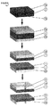
第1の実施形態において、ワークピース2は商業的に入手可能な単結晶シリコンウエハである。図2は、4工程(上部から下部へ)の本発明による代表的なプロセス順序を斜視図において図式的に示す。以下において、図2が参照される。
In the first embodiment, the
工程1:ここでの基本的原材料は、例えばマイクロエレクトロニクスまたは太陽光発電産業で使用されるような、チョクラルスキー法に従って生産された単結晶シリコンウエハ2である。ウエハ2は、約76mmの直径および約0.4mmの厚みを有する。ウエハは軽くnドープまたはpドープされ、約10オームcmの特異的電気抵抗率を有し、その2つの表面1aおよび1bは<100>結晶面に平行に配向される。ウエハの1つまたは両方の表面1aおよび/または1bは、鏡面研磨または単純にエッチングしてラップすることができる。ウエハ2はウエハ生産からそのまま使用することができるか、またはそれは従来の方法を使用して(例えば有機溶媒および水でまたはプラズマ酸化洗浄によって)荒く予備洗浄することができる。
Step 1: The basic raw material here is a single
工程2:ウエハ2aの各表面1aおよび1b上に、ポリジオルガノシロキサン(例えばポリジメチルシロキサン(またはPDMS);続く考察では便宜上PDMSを指すが、任意の好適なシリコーン重合体または共重合体を使用できることを理解すべきである)の薄層3aおよび3bを適用し硬化させる(または硬化を可能にする)。これらの補助層3aおよび3bの好ましい厚みは0.01mm〜10mmの間であり、約0.1mm〜約1mmの間の厚みがより好ましい。2つの層3a、3bの厚みはこの例示的な実施形態において同じであるが、他の実施形態において、2つの層の厚みは異なり得る。PDMSについては、例えばDow Corning社によるSYLGARD 184を、硬化剤と基部材との間の1:10の混合比で、使用することが可能である。液体のPDMS混合物を最初に真空中で約1時間脱気し、次いでそれを所望される厚みでウエハ2の各表面1a、1b上に適用し、ホットプレート上で硬化させる(例えば100℃で30分間)。この例示的な実施形態において、PDMS層3a、3bは大部分のウエハ領域にわたって均質の厚みを有する。これは、水平表面上にウエハを置くこと、およびそれを硬化させる前に重力によってPDMSを平衡化させることによって達成することができる。PDMSを硬化させた後に、3層複合物(PDMS 3a−ウエハ2−PDMS 3b)を室温まで冷却する。その後に、ウエハ2の縁部にPDMSが本質的にはなく、PDMSがウエハ2の2つの表面1a、1bのみを覆うように、ウエハ2の周面に沿って突出するPDMSを鋭いナイフで除去する。任意のPDMSをウエハ表面にPDMSを慎重に適用し水平表面上にそれを平衡化させることによって、ウエハの周面を超えて突出させない(およびしたがってウエハの縁部に接触する)ようにすることが可能であり、このような手段で、PDMSの表面張力はそれがウエハ縁部へオーバーフローしないようにする。
Step 2: On each
工程3:複合物(PDMS 3a−ウエハ2−PDMS 3b)を、液体窒素浴(温度、約−200℃)中に完全に浸漬する。シリコン(約3*10-6K-1)およびPDMS(約300*10-6K-1)の大きく異なる熱膨張率のために、この冷却によって、複合物中に大きな機械的応力が誘起される。PDMS層3a、3bが周囲の液体窒素浴との熱平衡に実質的に到達した後(例えばPDMS層3a、3bの周囲の液体窒素中の激しい「バブリング」がやむとき)、複合物を再び液体窒素浴から取り出し、室温に露出し、非常に短時間放置して加温する。この加温時間は、好ましくは、少なくともPDMS層3aおよび3bのある部分がまだPDMS(−125℃)のガラス転移温度未満の温度であるように十分に短く、および少なくともPDMS層3a、3bのある部分がPDMSのガラス転移温度より上の温度に達するように十分長く選択される。例えば、好ましい加温時間はPDMSの0.4mm厚の層については1〜5秒である。これは補助層の内側で非均質な物理的条件をもたらし、すなわち、PDMS層3aおよび3bの内側の温度分布は、およそ室温から約−200℃までの範囲の温度で非均質である。PDMSのガラス転移温度が約−125℃であり、PDMSがガラス転移温度未満の温度で比較的より剛性に(すなわちより大きな弾性率)なるので、これは、ウエハ2との界面に向かってより剛性で(すなわちより大きな弾性率)であり、外側でより柔軟(より低い弾性率)である、PDMS層3aおよび3bをもたらす。
Step 3: The composite (
工程4:短い加温時間後に、ウエハ2を、PDMS層3aおよび3bによって覆われない、ウエハ2の側面の特異的位置で(すなわちその縁部に沿った点で)、例えば鋭いとがったハンマー(ピーニング)により叩く。これはウエハ2中に局所的な脆弱域または欠損をもたらし、それは次には以下の破壊プロセスを引き起こす。ウエハ2は、その表面1aに平行に、2つの薄い単結晶シリコンディスク5へと、実質的に単一で中断されない亀裂伝播移動で自然に割裂し、各ディスク5の1つの側面は、対応するPDMS補助層3aまたは3bがまだ接着されている。
Step 4: After a short warm-up time, the
適切な配慮をすれば、2つのシリコンディスク5の各々は1つの単一ピースから本質的にはなる。表面4に垂直な追加の破損を回避するために、ディスク5は、割裂後に直接、全PDMS補助層が少なくとも室温まで再び加温されるまで、100℃のホットプレート上に((PDMS補助層3aまたは3bが接着された側面を下に面して)移動させることができる。どんな加温手順が用いられても、ディスク5は、加温されるにつれて、層のカーリングを戻すように平らな支持に対して慎重にプレスして加温が進行するにつれて層を平らにすることは好ましい。
With proper care, each of the two
この方法に従って生産された薄シリコンディスク5は、オリジナルのウエハ2と同じ特性を備えた単結晶シリコンから実質的になり、直接使用することができる。あるいは、PDMS補助層3aまたは3bは、例えば適切な液体エッチング液(例えばNMP(N−メチルピロリドン)およびTBAF/THF(テトラブチルフッ化アンモニウムのテトラヒドロフラン中の1.0M溶液)の容積で3:1の混合物)中での浸漬によって、またはフッ化水素酸中の浸漬によっても、シリコンディスク5から除去することもできる。PDMS補助層3aまたは3bを除去するための好ましい手段は、好ましくは150℃より上の(より好ましくは200℃より上の)温度の熱硫酸(H2SO4)エッチング液によりリンスすることまたは熱硫酸浴中で浸漬すること、次いで生産された白色シリカフォームを機械的に(例えばブラシおよび場合によっては複数のブラッシング−エッチングサイクルを使用して)除去すること、および最終的にフッ化水素酸中での浸漬によってシリコンディスク5を洗浄することである。
The
第2の例示的な実施形態において、複合物(PDMS 3a−ウエハ2−PDMS 3b)を液体窒素浴中にまだ浸漬しながら(すなわち冷却の間または周囲の液体窒素浴との熱平衡が到達された後)、破壊開始工程(工程4)を実行する。この実施形態において、短い中間の加温時間は省かれる。
In a second exemplary embodiment, thermal equilibrium was reached while still cooling the composite (
第3の例示的な実施形態において、工程4の間に鋭いとがったハンマーによりウエハに2を叩くとき、熱により誘起された応力が破壊を開始させるのに十分に大きくないように、工程3の加温時間を延長することができる。このケースにおいて、工程4を実行した後(破壊が起こらずに)、複合物(PDMS 3a−ウエハ2−PDMS 3b)は、液体窒素浴の中へ浸漬することによって再び冷却され、次いでそれは破壊プロセスの自発的開始をもたらす。
In a third exemplary embodiment, when hitting the
第4の例示的な実施形態において、工程4の間にウエハ2において局所的な脆弱域または欠損を作成することに加えてまたはその代わりに、外部応力を複合物(PDMS 3a−ウエハ2−PDMS 3b)の外側の特定の位置で適用し、次いでそれはウエハ材料の破壊靭性閾値より上の応力強度を局所的に増加させることによって、破壊(スポーリング)プロセスを引き起こす。
In a fourth exemplary embodiment, external stress is applied to the composite (
第5の例示的な実施形態において、ウエハ2における局所的な脆弱域または欠損は冷却工程(工程3)前に作成される。この実施形態において、脆弱域の作成は破壊プロセスを引き起こさないが、一旦十分な応力が工程3においてウエハ2を冷却することによってウエハ2において確立されたならば、破壊が好ましく開始する位置が規定されることを可能にする(次いで破壊はこのケースにおいては自然に開始するが、上記の方法のいずれかを使用してさらに引き起こすことができる)。
In the fifth exemplary embodiment, local weakened areas or defects in the
第6の実施形態において、ウエハ2のCTEとは実質的に異なるCTEを備えたPDMS層3aを有し、および温度変化に複合物構造をさらす代わりに、ウエハ2において要求される応力パターンを誘起できるPDMS層3aにおけるあらかじめ規定可能な応力パターンを生成するために他のメカニズムを使用することも可能である。かかる1つの代替方法は、PDMS層3aにおける特定の位置で圧電アクチュエータを含むこと、およびそれらを電気的に動作させてPDMS層3aにおいて応力パターンを生成することである。より一般的には、局所的に規定可能な応力パターンは、化学的または物理的メカニズムによって活性化された場合に異なる体積変化を行う異なる材料のパターンをPDMS層3aへと組み込むことによって生産することができる。かかる体積変化を達することができるメカニズムは、温度変化に加えて、湿度の変化(例えば膨潤、脱水和)、溶媒組成物および/またはイオン強度の変化(例えば浸透圧アクチュエータ、多価電解質ゲル、イオン性重合体金属複合物、導電性重合体、カーボンナノチューブアクチュエータ)、pH変化、相変化(例えば組み込まれた溶媒の凍結、結晶化、蒸発)、化学反応(例えば重合体ゲル)、電気的活性化(例えば圧電材料または電歪材料、静電アクチュエータ、電気活性重合体)、磁性活性化(例えば「磁性」ゲル)、光学的活性化(例えば液晶エラストマー、 光反応性材料)等と同様に、それらのいずれかまたはすべての組み合わせを含む。さらに、局所的にPDMS層3aの中へ異なる材料を組み込む代わりに、例えば重合体に対して異なる機能的側鎖を局所的に加えることまたは例えばUV照射によって架橋度を局所的に変化させることによって、所望される局所的に異なる容積変化挙動を達成するために、(化学的に)PDMS自体を局所的に修飾することは可能である。
In the sixth embodiment, it has a
第7の実施形態において、本方法は、2つの表面1aまたは1bの少なくとも1つの上に既存の表面構造を有するウエハ2上で使用される。かかる既存の表面構造(トレンチ、メサ、膜、カンチレバー、ピラミッド等)は、ウエハ材料それ自体から形成することができるか、またはそれらは追加材料(例えば金属接触、反射防止層、誘電体層、エピタキシャル層等)、またはその任意の組み合わせを含むことができる。次いでPDMSを既存の構造に対して適用し、それらを覆い等角的に囲んで、PDMSの硬化後に、既存の構造をPDMS層3aおよび/または3b中に部分的に組み込まれるようにする。ウエハ2が2つの薄ディスク5へと割裂する場合、既存の表面構造は、対応するPDMS補助層3aまたは3bがまだ接着される各ディスク5の側面上に維持される。このような手段で、1つの側面上に複雑な表面構造(場合によっては追加材料を含み、電子デバイス、光学デバイス、化学デバイスまたはマイクロメカニカルデバイス等の完全に機能的なデバイスをも提供する)。を備えた薄い独立層を生産することができる。
In a seventh embodiment, the method is used on a
第8の実施形態において、本方法は、例えば1つまたは複数のドーパント勾配等の既存の内部(バルク)構造を有するウエハ2上で使用される。ウエハ2が2つの薄ディスク5へと割裂する場合、既存の内部構造は対応する薄ディスク5中に維持される。このような手段で、ドーパント勾配等の内部(バルク)構造を有する薄独立層を生産することができる。
In an eighth embodiment, the method is used on a
第9の実施形態において、先の2つの実施形態からの態様を組み合わせて、本方法は、既存の表面構造および既存の内部(バルク)構造の両方を有するウエハ2上で使用される。特に、ウエハは、その表面1aおよび/または1bの1つまたは両方上に機能的なデバイス(電子デバイス、光学デバイス、マイクロメカニカルデバイス、化学デバイス等)を部分的にまたは完全に有している。かかるデバイスは、LED、レーザーダイオード、太陽電池、タンデム太陽電池、電力増幅器、集積回路一般、センサまたはアクチュエータ等のマイクロエレクトロメカニカルデバイス等を含むことができる。次いでPDMSはウエハ表面上の既存のデバイスに対して適用し、デバイスを覆い、外側で等角的にそれらを囲んで、PDMSの硬化後に、既存のデバイスをPDMS層3aおよび/または3b中に部分的に組み込まれるようにする。ウエハ2が2つの薄ディスク5へと割裂する場合、既存のデバイスは、対応するPDMS補助層(3aまたは3bのそれぞれ)がまだ接着される各ディスク5の側面上に維持される。このような手段で、1つの側面上に複雑で、部分的にまたは既に完全に機能的なデバイスを有する薄い独立層を生産することができる。
In a ninth embodiment, combining the aspects from the previous two embodiments, the method is used on a
先の実施形態の適用のための例示的な例として、従来のシリコン太陽電池(例えばpn接合、前面の金属接触グリッド、抗反射コーティングを含む前側ドープ層)の前方部を構築する表面構造および内部構造が考慮され、以下において「前部構造」と称される。ここで、ウエハの1つの側面上にのみこれらの「前部構造」を従来通りに生産する代わりに、かかる「前部構造」は、厚い単結晶シリコンウエハ2の両側面1aおよび1b上に製造される。次いでこのウエハ2は上記されるような2つの薄ディスク5へと割裂し、それによってデバイス層は維持されて、ここでこれらの2つのディスク5の各々は「前部構造」を有するが、1つの側面(すなわち、対応するPDMS層3aまたは3bがまだ接着される側面)上でのみ有するようにする。2つのディスク5の各々の他の側面上に、バルクウエハ材料からなる「新たな」表面がある。両方のディスクの「新たな」表面は、シリコン太陽電池の裏側の作製のために従来の方法を使用してさらに加工することができ(例えば裏面電界ドーピングおよび裏側接触金属化等)、2つのシリコン太陽電池の製造が完了する。この実施例は以下の多数の利点を示す。大部分の太陽電池製造工程は、比較的厚い(およびそれゆえ脆弱でない)ウエハ2上で行うことができ、それは接触スクリーン印刷等の低費用のプロセスの使用を促進し、一般に扱われるウエハを単純化する。さらに、同じ(前側)ドーパントは、ウエハの全表面へと(すなわちその側面1aおよび1bの両方へと)拡散させることができ、例えばウエハの裏からドーパントを続いて除去する必要はない(それが割裂プロセスによって自動的に達成されるので)。同じことは例えば反射防止コーティングの場合にも言え、それは全ウエハ上で生産することもでき(例えばSiO2の酸化成長および/またはSi3N4窒化物のPECVD被着)、次いで割裂プロセスを介して1つの側面に自動的に制限される。このような手段で、太陽電池製造のための多数の加工工程は、本方法の適用によって排除または単純化することができる。前部および背部の接触を備えた標準的な太陽電池の代わりに裏面接触太陽電池が製造される場合、これらの利益は別の例示的な例において特に著しい。本明細書において、機能的構造のほとんどすべては電池の1つの側面(裏側)上にある。かかる裏側構造が厚い単結晶シリコンウエハ2の両方の表面1aおよび1b上に製造されるならば、本方法を使用した割裂後の、生産された薄ディスク5は両方は既にほとんど完成した裏面接触電池になる(恐らく他の側面上に反射防止コーティングの被着のみを必要とする)。それゆえ、プロセスの大部分を介して薄ウエハを扱う必要なしに、薄い単結晶シリコン裏面接触太陽電池を生産することに、本方法を適用することができる。
As an illustrative example for the application of the previous embodiment, the surface structure and interior that build the front of a conventional silicon solar cell (eg, pn junction, front metal contact grid, front doped layer including anti-reflective coating) The structure is considered and is referred to below as the “front structure”. Here, instead of producing these “front structures” conventionally only on one side of the wafer, such “front structures” are produced on both side faces 1 a and 1 b of the thick single
別の態様において、本発明は、2ピース(1ピースは他のピースの幾何学的な相補物である)へとギャップによって分割した固体状材料のスラブ(ブロック、インゴット、ディスク等)を含み、ギャップをゼロまで減少させることによって、実質的に欠損した材料(例えば内部空隙等)なしで、オリジナルのスラブの形状および寸法および重量を取り戻すことができるようにしたデバイスに関する。それらの2ピースの少なくとも1つは、薄層(すなわち、実質的に水平または湾曲した少なくとも1cm2の領域を有し、その厚みがこの領域の全体にわたって2mm未満、好ましくは0.5mm未満であるシート)である。薄層ピースの少なくとも1つのそれ自体は、ギャップの反対の表面上で、局所的に変動する材料特性(例えば局所的に変動する弾性率)を備えた少なくとも1つの追加の固体状材料(補助層)の層をそれに接着する。2ピースの各々については、ギャップに面する表面は、スラブのバルクにおいて見出されるもの以外の材料を含有しない(場合によっては、例えば表面が大気と反応性で大気に露出されるならば、天然の酸化層を除いて)。 In another aspect, the invention includes a slab (block, ingot, disk, etc.) of solid material divided by a gap into two pieces (one piece being the geometric complement of the other piece), It relates to a device that allows the shape, size and weight of the original slab to be regained without substantially missing material (such as internal voids) by reducing the gap to zero. At least one of those two pieces has a thin layer (ie, a substantially horizontal or curved region of at least 1 cm 2 and a thickness of less than 2 mm, preferably less than 0.5 mm throughout this region. Sheet). At least one of the thin layer pieces is itself at least one additional solid material (auxiliary layer) with locally varying material properties (eg locally varying elastic modulus) on the opposite surface of the gap. Adhere the layer of) to it. For each of the two pieces, the surface facing the gap contains no material other than that found in the bulk of the slab (in some cases, for example if the surface is reactive to the atmosphere and exposed to the atmosphere, the natural Except the oxide layer).
本発明のアプローチは、単結晶シリコン以外の固体状材料(例えば多結晶シリコン、サファイア、ゲルマニウム、石英、酸化亜鉛またはガラス等の非晶質材料)からなるワークピースから薄独立層を生産するのに使用することができる。さらに、このアプローチは、複数の異なる材料(均質または非均質の複合物材料等)からなるワークピース、または内部構造(ラミネート等)を有するワークピースと共に使用することができる。さらに、ワークピース上に適用される補助層については、PDMS以外の材料(例えば、他のポリシロキサン(例えば電気活性のための有機金属基を含むことができる)、他のエラストマー、他の重合体もしくはプラスチック一般、またはアルミニウムもしくは銀等の金属等)を使用することができる。複数の異なる材料(均質または非均質の複合物材料等)からなる補助層、または内部構造(ラミネート等)を有する補助層を利用することも可能である。一般に、ワークピースは比較的脆弱な固体状材料である。ワークピースと補助層との間の優れた接着はプロセスの全体にわたって達成され維持されるべきであり、補助層は、補助層それ自体が破損されることなく十分に強い応力パターンを課するのに好都合なプロセスに従うべきである。 The approach of the present invention is to produce a thin independent layer from a workpiece made of a solid material other than single crystal silicon (eg, amorphous material such as polycrystalline silicon, sapphire, germanium, quartz, zinc oxide or glass). Can be used. Furthermore, this approach can be used with workpieces made of a plurality of different materials (such as homogeneous or non-homogeneous composite materials), or workpieces having an internal structure (such as a laminate). In addition, for auxiliary layers applied on the workpiece, materials other than PDMS (eg other polysiloxanes (eg can contain organometallic groups for electroactivity), other elastomers, other polymers) Alternatively, plastic in general, or a metal such as aluminum or silver) can be used. It is also possible to use auxiliary layers made of a plurality of different materials (such as homogeneous or non-homogeneous composite materials) or auxiliary layers having an internal structure (such as a laminate). In general, the workpiece is a relatively fragile solid material. Excellent adhesion between the workpiece and the auxiliary layer should be achieved and maintained throughout the process, and the auxiliary layer imposes a sufficiently strong stress pattern without damaging the auxiliary layer itself. You should follow a convenient process.
さらに、補助層におけるPDMS(または他の重合体)は、ホットプレート上での加熱以外の手段によって硬化(すなわちその重合体鎖の架橋)させることができる。例えば、その上に高温ガスを送風すること、または例えば赤外光により照射することによって加熱することができる。あるいはまたは加えて、硬化は、化学添加剤、紫外線または電子線を使用して遂行することができる。PDMS(もしくは他の重合体、または一般に補助層における任意の材料)を化学的に修飾して、硬化の特定の形態(または一般に凝固、場合によっては凝固の間に既に層の内側に内部応力を生成する)を促進することができ、例えば、UV照射による硬化PDMSは、例えばベンゾフェノン(照射下でラジカルを生成する光増感剤)中のPDMSの浸漬によって、または例えばPDMS中のメチル基を光反応性の置換基と置換することによって促進することができる。 Further, the PDMS (or other polymer) in the auxiliary layer can be cured (ie, the polymer chains cross-linked) by means other than heating on a hot plate. For example, it can be heated by blowing hot gas over it, or by irradiating it with infrared light, for example. Alternatively or additionally, curing can be accomplished using chemical additives, ultraviolet light or electron beams. PDMS (or other polymer, or generally any material in the auxiliary layer) can be chemically modified to create a specific form of cure (or generally solidification, and possibly internal stress inside the layer already during solidification). For example, cured PDMS by UV irradiation can, for example, immerse PDMS in benzophenone (a photosensitizer that generates radicals under irradiation) or photomethylate methyl groups in PDMS, for example. This can be facilitated by substitution with reactive substituents.
同様に、多数の代替方法は使用してプロセスの終了時にディスク5から補助層を除去することができる。上記されるような補助層を化学的エッチングで除去する代わりに、またはそれに加えて、この層は、照射、電子線、および/または熱によって、機械的に除去することができる。例えば、PDMS層の反対のディスクの表面を一時的に支持に固定する(例えば固着する)ならば、薄ディスク5からPDMS補助層を機械的に割裂させることができ、例えば次いで角から開始してPDMSをディスクの表面に対して実質的に垂直な方向で引っ張ることによってゆっくり慎重に割裂させる。あるいは、PDMS(または他の重合体)を、その分解温度より上に、例えばレーザーにより、またはオーブン中で単純に加熱することができる(すなわち灰化による除去)。それはプラズマ中の(例えば酸素プラズマ中の)灰化によっても除去することができる。PDMSが例えばUV照射の下でまたは熱に対して露出した場合、容易に分解するように化学的に修飾することもできる。最終的に、これらのアプローチのいずれかまたはすべてを組み合わせることができる(PDMS以外の材料が補助層のために使用されるならば、直接に適合される)。
Similarly, a number of alternative methods can be used to remove the auxiliary layer from the
本アプローチは、ほとんど任意の形状のワークピースに適用することができ、平面のウエハに限定されていない(特に、本発明を使用して、例えば1つの側面上で平らにされた単結晶シリコンインゴットから薄シートを直接割裂することができる)。平らなシートを割裂させるには、使用されるワークピースが少なくとも1つの平らな表面によって制限されることで十分である。次いでこの界面上に補助層を適用する。1つのシートのみを割裂させることが可能であるか、またはワークピースの異なる界面から複数のシートを同時に割裂させることが可能である。最終的に、本アプローチは薄く独立した湾曲したシートまたはシェルの生産にも適用することができる。この目的のために、補助層はワークピースの対応して湾曲した表面上に適用される。次いで、温度変化(または他の応力を誘起するプロセス)は、ワークピースの内側でパターン形成された破壊域に沿って、ワークピースの残りからの薄く対応して湾曲したシートまたはシェルの割裂をもたらす。このパターン形成された破壊域は、ワークピースと補助層との間の界面におよそ同じ距離で至る所に広がり、その結果表面構造パターンを備えた生産されたシートはおよそ均一の厚みを有する。 The approach can be applied to almost any shape of workpiece and is not limited to planar wafers (in particular, using the present invention, for example, a single crystal silicon ingot flattened on one side The thin sheet can be split directly from). To split a flat sheet, it is sufficient that the workpiece used is limited by at least one flat surface. An auxiliary layer is then applied over this interface. Only one sheet can be split or multiple sheets can be split simultaneously from different interfaces of the workpiece. Finally, this approach can also be applied to the production of thin and independent curved sheets or shells. For this purpose, an auxiliary layer is applied on the corresponding curved surface of the workpiece. The temperature change (or other stress-inducing process) then results in a thin correspondingly curved sheet or shell split from the rest of the workpiece along the patterned fracture zone inside the workpiece. . This patterned fracture zone extends at approximately the same distance to the interface between the workpiece and the auxiliary layer so that the produced sheet with the surface structure pattern has an approximately uniform thickness.
補助層が適用される界面の表面性質は重要ではない。界面は滑らかに研磨することができるか、または著しい粗度を有することができる。補助層に対する適切な接着を保持することのみが重要である。特に、破壊面(ワークピースからのシートから割裂する場合にワークピースの残りの上で形成される)は、補助層が適用される界面として続いて使用することができる。したがって、本アプローチは、ワークピースの残り上で再び適用することができる。このような手段で、単一ワークピースから、シートの後にまたシートを連続的に割裂させることができる。 The surface properties of the interface to which the auxiliary layer is applied are not critical. The interface can be polished smoothly or have a significant roughness. It is only important to maintain proper adhesion to the auxiliary layer. In particular, the fracture surface (formed on the rest of the workpiece when splitting from the sheet from the workpiece) can subsequently be used as an interface to which the auxiliary layer is applied. Thus, this approach can be reapplied on the rest of the workpiece. By such means, it is possible to continuously split the sheet again after the sheet from a single workpiece.
さらに、割裂された薄独立層から、同じ工程の反復によって、(より薄い)層をさらに割裂させることができる。例えば、本方法を使用して、単結晶シリコンウエハは、両側上にPDMS補助層を適用することによって2つのディスクへと割裂させることができる。次いでこれらの2つのより薄いディスクの各々を、再びPDMS補助層を備えた両側上に提供することができ、この方法の工程を反復して、したがって2つのなおより薄いディスクへとさらに割裂させること等が可能である。このような手段で、非常に多数の薄い単結晶ディスクは単一単結晶シリコンウエハから得ることができる。例えば、3工程で、約50マイクロメートル厚の8つのディスクを従来の0.4mm厚のウエハから得ることができる。 Furthermore, the (thinner) layer can be further split from the split thin independent layer by repeating the same process. For example, using this method, a single crystal silicon wafer can be split into two disks by applying a PDMS auxiliary layer on both sides. Each of these two thinner discs can then be provided again on both sides with a PDMS auxiliary layer and the process steps are repeated thus further splitting into two even thinner discs Etc. are possible. By such means, a very large number of thin single crystal disks can be obtained from a single single crystal silicon wafer. For example, in three steps, eight disks about 50 micrometers thick can be obtained from a conventional 0.4 mm thick wafer.
一般に、このように生産された薄い独立層の寸法、特に、それらの厚みは、応力を誘起するメカニズム(例えば温度変化)および/または補助層の特性の適切な選択を介して定めることができる。これは、応力誘導のタイムフロー、誘起された応力の大きさ、補助層の寸法、補助層の幾何学的形状、ならびに/または局所的な機械的および/もしくは局所的な熱/化学的/静水学的/圧電/等の補助層の特性の適切な選択を介して特に達成される。 In general, the dimensions of the thin stand-alone layers produced in this way, in particular their thickness, can be determined through appropriate selection of stress-inducing mechanisms (eg temperature changes) and / or auxiliary layer properties. This may include stress-induced time flow, magnitude of induced stress, auxiliary layer dimensions, auxiliary layer geometry, and / or local mechanical and / or local thermal / chemical / hydrostatic This is achieved in particular through an appropriate selection of the properties of the auxiliary layer, such as chemistry / piezoelectric / etc.
補助層は、ワークピースの対応する界面上に例えば液体または気体の状態で適用され、次いでそこで凝固させることができる。あるいは、補助層は界面上に固体状態で直接接着することもできる。補助層と界面との間の接着は、化学結合、ファンデルワールス力または他の強い接着力を介して達成することができる。さらに界面での補助層およびワークピース材料の合金化を介する接着、またはワークピースの界面上への第3の材料(例えば接着剤)を用いた補助層の接着は、本方法の実装で可能である。 The auxiliary layer can be applied, for example in liquid or gaseous state, on the corresponding interface of the workpiece and then solidified there. Alternatively, the auxiliary layer can be bonded directly in the solid state on the interface. Adhesion between the auxiliary layer and the interface can be achieved via chemical bonds, van der Waals forces or other strong adhesion forces. Furthermore, adhesion through the alloying of the auxiliary layer and workpiece material at the interface, or adhesion of the auxiliary layer with a third material (eg adhesive) onto the workpiece interface is possible with the implementation of the method. is there.
最終的に、液体窒素の代わりに、他の冷却液(例えば液体ヘリウム、氷水、または冷却固体もしくは冷却気体等)を使用して、補助層−ワークピース複合物の内側で必要な機械的応力を冷却によって確立することができる。特定のケースにおいて、複合物を単純により高い温度から室温へ冷却することで十分であり、その結果特殊な冷却液が必要でない。さらに、特定のケースにおいて、冷却の代わりに加温によって複合物の内側で必要な機械的応力を達成することが可能である。特定の温度Tで必要な機械的応力の確立に必須なことは、ワークピースと少なくとも一部の補助層との間の熱膨張の十分に大きな差に加えて、温度Tと補助層がワークピース上へ接着された温度との間の十分に大きな差である。 Finally, instead of liquid nitrogen, other cooling liquids (such as liquid helium, ice water, or a cooling solid or cooling gas) are used to provide the necessary mechanical stress inside the auxiliary layer-workpiece composite. Can be established by cooling. In certain cases, it is sufficient to simply cool the composite from a higher temperature to room temperature, so that no special coolant is required. Furthermore, in certain cases, it is possible to achieve the required mechanical stress inside the composite by heating instead of cooling. Essential to establishing the required mechanical stress at a particular temperature T is that, in addition to a sufficiently large difference in thermal expansion between the workpiece and at least some of the auxiliary layers, the temperature T and the auxiliary layers are It is a sufficiently large difference between the temperature bonded to the top.
本発明のこの独立した実施形態によれば、ワークピースからの応力に誘起された割裂(スポーリング)による固体状材料の薄い独立層の生産は、重合体等の低費用で低混入の材料を含む、応力を誘起する補助層の使用を可能にする方法の提供によって改善される。本発明の実施形態は、かかる材料を使用するための上記の難点を減少させる、単純で低費用のプロセスを提供する。 According to this independent embodiment of the present invention, the production of a thin, independent layer of solid material by stress-induced splitting (spalling) from the workpiece allows for low cost and low contamination materials such as polymers. Improved by providing a method that allows the use of a stress-inducing auxiliary layer. Embodiments of the present invention provide a simple and low cost process that reduces the above difficulties for using such materials.
様々な実施形態において、固体状材料の薄い独立層は、異なる材料特性(例えば異なる熱膨張率(CTE))を有する固体素地を互いに接着することで、物理的または化学的な変化(例えば温度変化)によって誘起される機械的応力の使用によって生産される、この目的に対して、固体状材料(好ましくは100MPaを超える、より好ましくは1GPaを超える弾性率を有する)からなるワークピースに加えて、温度変化および/または外部圧力変化等の物理的変化の特定の順序にさらされる場合、ワークピースが同じ順序の物理的変化にさらされる場合のワークピースの対応する変化とは実質的に異なる手段で、物理的寸法(例えばその容積)が変化する別の固体物質(例えばその熱膨張がワークピースの熱膨張とは実質的に異なる固体物質)が使用され、それは強い接着を介してワークピースに接合することができる。この追加材料(以下において「補助層」と称される)の1つの層は、ワークピースの表面上へ接着される。次いで、ワークピースおよび補助層からなる複合物構造は、温度変化および/または外部圧力変化等の物理的変化の順序にさらされる。適切な条件の下では、複合物構造においてこのように誘起される機械的応力は、ワークピースと補助層との間の界面に実質的に平行に、ワークピースからの薄層の割裂(「スポーリング」)をもたらす。固体状材料の割裂した薄層の領域は、補助層の領域とほぼ一致する。薄層がワークピースから割裂する場合に形成された2つの表面の各々は、再び使用することができる(すなわち、別の補助層を、ワークピースの新しく露出した表面または割裂した層の新しく露出した表面に適用することができる)。したがって、本発明の実施形態は、ワークピースの残りおよび割裂した層の両方からの割裂操作の反復を促進して、さらなる(およびより薄い)層を生成する。さらに、ワークピース(例えば薄シートから実質的になるワークピース、例えばウエハ)のいくつかの例については、例えば安定性を促進し、ワークピースの残りの粉砕を回避するために、固体状材料のワークピースの2つまたはそれ以上の(場合によっては反対の)表面上に補助層を形成することは有利であり得る。 In various embodiments, a thin, independent layer of solid-state material can be used to bond physical bodies with different material properties (eg, different coefficients of thermal expansion (CTE)) to each other to change physical or chemical changes (eg, temperature changes). For this purpose, produced by the use of mechanical stress induced by)), in addition to a workpiece consisting of a solid material (preferably having a modulus of elasticity above 100 MPa, more preferably above 1 GPa), When exposed to a particular sequence of physical changes, such as temperature changes and / or external pressure changes, in a substantially different manner than the corresponding changes in the workpiece when the workpieces are exposed to the same sequence of physical changes Another solid material whose physical dimensions (eg its volume) vary (eg a solid whose thermal expansion is substantially different from that of the workpiece) Quality) is used, it can be joined to the workpiece through a strong adhesion. One layer of this additional material (hereinafter referred to as “auxiliary layer”) is glued onto the surface of the workpiece. The composite structure consisting of the workpiece and the auxiliary layer is then subjected to a sequence of physical changes such as temperature changes and / or external pressure changes. Under appropriate conditions, the mechanical stresses thus induced in the composite structure can cause a thin layer split ("scaling" from the workpiece substantially parallel to the interface between the workpiece and the auxiliary layer. Polling "). The region of the split thin layer of the solid material substantially coincides with the region of the auxiliary layer. Each of the two surfaces formed when the thin layer splits from the workpiece can be used again (i.e., another auxiliary layer can be used for the newly exposed surface of the workpiece or the newly exposed layer of the split layer). Can be applied to the surface). Thus, embodiments of the present invention facilitate the repetition of the splitting operation from both the rest of the workpiece and the split layer to produce additional (and thinner) layers. Further, for some examples of workpieces (eg, workpieces consisting essentially of thin sheets, eg, wafers), for example, to promote stability and avoid remaining crushing of the workpiece, It may be advantageous to form an auxiliary layer on two or more (possibly opposite) surfaces of the workpiece.
例えば、要求される機械的応力を誘起するために1つまたは複数の温度変化が使用されるならばワークピースと補助層との間のCTEの絶対差は、室温で5*10 −6 K −1 を超え、好ましくは室温で50*10 −6 K −1 を超え、より好ましくは室温で100*10 −6 K −1 を超え、最も好ましくは室温で200*10 −6 K −1 を超える。
ワークピースおよび補助層の両方が融解することまたは分解することまたは互いに接着しなくなることなく、温度(例えばプラスマイナス400℃以上)において大きな絶対的相違を維持することができるならば、CTEの比較的小さな絶対差を使用することができるが、CTEのより大きな絶対差が好ましい(例えばより高温度の使用は拡散による交差混入のリスクを増加させ得るので)。例えば、ワークピースは室温で約3*10 −6 K −1 のCTEを持つシリコンからなり得、補助層は室温で約10*10 −6 K −1 を超えるCTEによって特徴づけられる重合体を含むことができる。好ましくは、重合体は室温で約50*10 −6 K −1 を超えるCTEによって特徴づけられ、より好ましくは、重合体は室温で約200*10 −6 K −1 を超えるCTEによって特徴づけられる。例えば、補助層は室温で約300*10 −6 K −1 のCTEを有する架橋されたポリジメチルシロキサン(PDMS)からなり得る。
For example, if one or more temperature changes are used to induce the required mechanical stress, the absolute difference in CTE between the workpiece and the auxiliary layer is 5 * 10 −6 K − at room temperature. Greater than 1 , preferably greater than 50 * 10 −6 K −1 at room temperature, more preferably greater than 100 * 10 −6 K −1 at room temperature, and most preferably greater than 200 * 10 −6 K −1 at room temperature. .
If a large absolute difference in temperature (eg, plus or minus 400 ° C. or more) can be maintained without both the workpiece and the auxiliary layer melting or decomposing or not sticking to each other, Although small absolute differences can be used, larger absolute differences in CTE are preferred (eg, the use of higher temperatures can increase the risk of cross-contamination due to diffusion). For example, the workpiece may be composed of silicon having a CTE of about 3 * 10 −6 K −1 at room temperature, and the auxiliary layer comprises a polymer characterized by a CTE greater than about 10 * 10 −6 K −1 at room temperature. be able to. Preferably, the polymer is characterized by a CTE above about 50 * 10 −6 K −1 at room temperature, more preferably the polymer is characterized by a CTE above about 200 * 10 −6 K −1 at room temperature. . For example, the auxiliary layer may consist of a crosslinked polydimethylsiloxane (PDMS) having a CTE of about 300 * 10 −6 K −1 at room temperature.
本発明の様々な実施形態において、重合体等の低費用で低混入の材料を含む、応力を誘起する補助層の使用、特に、正常条件の下で比較的低い弾性率(例えば100MPa未満、場合によっては10MPa未満、または1MPa未満でさえ)および/または低い破壊靭性(例えば5MPa m1/2未満、場合によっては2MPa m1/2未満、または1MPa m1/2未満でさえ)を有する材料の使用を可能にする方法が提供される。 In various embodiments of the present invention, the use of stress-inducing auxiliary layers, including low cost, low contamination materials such as polymers, particularly relatively low moduli under normal conditions (eg less than 100 MPa, if Of materials having less than 10 MPa or even less than 1 MPa) and / or low fracture toughness (eg less than 5 MPa m 1/2 , in some cases less than 2 MPa m 1/2 or even less than 1 MPa m 1/2 ) A method is provided that enables use.
1つの例において、異なる材料を含む不均一な補助層を使用することができ、そこでは1つの材料は比較的高い弾性率を有するが高い破壊靭性を有するというわけではなく、別の材料は比較的高い破壊靭性を有するが高い弾性率を有するというわけではない。より正確には、不均一な層は異なる材料を含み、そこでは少なくとも1つの材料は比較的高い弾性率(すなわち10MPaを超え、好ましくは100Mpaを超えるおよびより好ましくは1Gpaを超える弾性率)を有し、少なくとも1つの材料は比較的高い破壊靭性(すなわちワークピース材料の破壊靭性の1/10を超え、好ましくはワークピース材料の破壊靭性を超える、およびより好ましくはワークピース材料の破壊靭性の10倍を超える破壊靭性)を有し、少なくとも1つの材料はその物理的寸法(例えばその容積)が温度変化および/または外部圧力変化等の物理的変化の特定の順序にさらされる場合、ワークピースが同じ順序の物理的変化にさらされる場合のワークピース材料の対応する変化とは実質的に異なって変化する特性を有し、(例えばそのCTEが、室温で少なくとも5*10 −6 K −1 、好ましくは室温で50*10 −6 K −1 を超えて、より好ましくは室温で100*10 −6 K −1 を超えて、および最も好ましくは室温で200*10 −6 K −1 を超えて、ワークピースのCTEとは異なる材料)単一材料はそれらの3つの全特性(すなわち高い弾性率、高い破壊靭性、およびワークピースとは実質的に異なる物理的寸法変化)を有するとは限らない。不均一な補助層中の異なる材料の相対濃度は、例えば補助層内の位置にも依存し得る(例えば、固体状材料のワークピースとの界面に接近するほど、高い弾性率を有する材料の濃度は高くなる)。例えば、不均一な補助層は液体PDMSの中に小さな(場合によってはナノ多孔性)微粒子シリカを混合すること、ワークピースの表面にこの混合物を広げること、および次いで例えば熱によって硬化させる(架橋)ことによって生成することができる。この例において、PDMSは室温で約100kPa〜3MPaの間の剪断弾性率および0.03〜4MPa m1/2の間の破壊靭性を有する。
微粒子シリカは、好ましくは0.5〜10マイクロメートルの間の直径、約20〜40GPaの間の剪断弾性率および0.1〜1MPa m1/2の間の破壊靭性、(すべて室温で)を有する。PDMSの微粒子シリカの濃度は重量で1%〜80%の間、好ましくは重量で10%〜30%の間である。別の例において、微粒子シリカは好ましくは補助層とワークピースとの間の界面に接近して位置させることができ、すなわち、PDMSマトリックス中のそれらの濃度は、界面に接近して最も高く、補助層の他の部分において低い(またはゼロ)。
In one example, a non-uniform auxiliary layer comprising different materials can be used, where one material has a relatively high modulus but does not have high fracture toughness, while another material is a comparative It has a high fracture toughness but does not have a high elastic modulus. More precisely, the heterogeneous layer comprises different materials, where at least one material has a relatively high modulus of elasticity (ie greater than 10 MPa, preferably greater than 100 Mpa and more preferably greater than 1 Gpa). And at least one material has a relatively high fracture toughness (ie, greater than 1/10 of the fracture toughness of the workpiece material, preferably greater than the fracture toughness of the workpiece material, and more preferably 10 of the fracture toughness of the workpiece material). If the workpiece has a physical dimension (eg, its volume) subjected to a specific sequence of physical changes such as temperature changes and / or external pressure changes, Features that change substantially differently from the corresponding changes in the workpiece material when exposed to the same sequence of physical changes. Have, (e.g., the CTE is at least 5 * 10 -6 K -1 at room temperature, preferably more than 50 * 10 -6 K -1 at room temperature, more preferably at room temperature 100 * 10 -6 K - A material that is different from the CTE of the workpiece, exceeding 1 and most preferably exceeding 200 * 10 −6 K −1 at room temperature) all three of these properties (ie, high modulus, high fracture) It does not necessarily have toughness and physical dimensional changes that are substantially different from the workpiece. The relative concentration of different materials in the non-uniform auxiliary layer may also depend on, for example, the position within the auxiliary layer (e.g., the concentration of a material having a higher modulus of elasticity as it approaches the interface with the solid material workpiece). Will be higher). For example, a non-uniform auxiliary layer can be mixed with small (possibly nanoporous) particulate silica in liquid PDMS, spreading this mixture over the surface of the workpiece, and then cured, for example by heat (crosslinking) Can be generated. In this example, PDMS has a shear modulus between about 100 kPa and 3 MPa and a fracture toughness between 0.03 and 4 MPa m 1/2 at room temperature.
The particulate silica preferably has a diameter between 0.5 and 10 micrometers, a shear modulus between about 20 and 40 GPa and a fracture toughness between 0.1 and 1 MPa m 1/2 , all at room temperature. Have. The concentration of the particulate silica of PDMS is between 1% and 80% by weight, preferably between 10% and 30% by weight. In another example, the particulate silica can preferably be located close to the interface between the auxiliary layer and the workpiece, i.e. their concentration in the PDMS matrix is highest close to the interface and the auxiliary Low (or zero) in other parts of the layer.
別の例において、異なる配合の同じ材料を補助層の異なる部分において使用することができる(例えば、異なる重合体鎖長を補助層内の位置に依存して使用する)。なお別の例において、異なる架橋度の重合体鎖を補助層内の位置に依存して使用することができる(局所的により高架橋度を使用して、ガラス転移温度を局所的に増加させ、すなわち、材料を補助層内のあらかじめ規定可能な位置でより剛性にすることができる)。局所的に異なる架橋度を備えたあらかじめ規定可能なパターンの領域は、特に光硬化可能な重合体を使用する場合、例えばマスクを介する紫外線源による選択照射を介して、または所望される領域一帯のUVレーザー光線の指向性よって、例えば作成することができる。 In another example, the same material of different formulations can be used in different parts of the auxiliary layer (eg, different polymer chain lengths are used depending on the position in the auxiliary layer). In yet another example, polymer chains with different degrees of cross-linking can be used depending on the position in the auxiliary layer (using a higher degree of cross-linking locally to increase the glass transition temperature locally, i.e. The material can be made more rigid at pre-definable positions in the auxiliary layer). Pre-definable pattern areas with locally different degrees of cross-linking, particularly when using photo-curable polymers, for example via selective irradiation with a UV source through a mask or over the desired area. Depending on the directivity of the UV laser beam, it can be created, for example.
別の例において、補助層中の材料は、例えば照射、熱、圧力または化学反応によって異なる弾性率および/または破壊靭性を有する別の材料に局所的に変換することができる。例えば、PDMSを実質的に含む補助層の表面の部分またはすべては、例えばUV照射、オゾン処理またはプラズマ酸化に対して露出される。適切な条件の下では、これは補助層におけるガラス質の表面層の形成を、実質的に露出された位置でもたらし(例えば−CH3基の−OH末端基官能基への転換に起因して)、この局所的に規定されたガラス質の表面層はよりガラス様の特性(すなわち、補助層の他の部分よりもより剛性である(より高い弾性率))を有する。 In another example, the material in the auxiliary layer can be locally converted to another material having a different modulus and / or fracture toughness, for example by irradiation, heat, pressure or chemical reaction. For example, part or all of the surface of the auxiliary layer substantially comprising PDMS is exposed to, for example, UV irradiation, ozone treatment or plasma oxidation. Under appropriate conditions, this results in the formation of a glassy surface layer in the auxiliary layer at substantially exposed positions (eg due to the conversion of —CH 3 groups to —OH end group functional groups). ), This locally defined glassy surface layer has more glass-like properties (ie, it is more rigid (higher modulus) than the rest of the auxiliary layer).
別の例において、実質的に単一材料を含む均質の補助層は使用することができる。この例において、破壊靭性および/または弾性率等のこの材料の関連する特性が補助層内の位置に依存して変動するように、物理的条件は提供される。例えば、重合体は、それらのガラス転移温度未満の温度で同等に高い弾性率(すなわち「より剛性」、例えば100MPaまたは1GPaを超える剪断弾性率を有する)であり、多くの場合比較的脆弱であり(すなわち低破壊靭性、例えば1MPa m1/2未満))、それらのガラス転移温度より上の温度で同等に低い弾性率(すなわち「より柔軟」、例えば100MPaまたは10MPa未満の剪断弾性率を有する)であるが、より展性がある(すなわち高破壊靭性、例えば1MPa m1/2よりも高い)。かかる重合体を含む補助層の内側のあらかじめ規定された温度分布プロファイル(例えば温度勾配)の設定によって(重合体のガラス転移温度はこの温度分布における最小値および最大値の間の温度である)、次いで補助層の材料は補助層の内側の特定のあらかじめ規定可能な位置でより展性のあるおよび/または「より柔軟」になるが、他のあらかじめ規定可能な位置で比較的より脆弱および/または「より剛性」になる。例えば、補助層を構成する重合体のガラス転移温度未満の温度でワークピースと接着補助層との間の界面を維持し、その一方でガラス転移温度より上の温度で補助層の反対の(「自由」)表面を維持することは、補助層を横切った温度勾配をもたらす。この例において、これは、より脆弱なおよび/または「より剛性」の界面に近い補助層の部分、およびより展性のあるおよび/または「より柔軟」な「自由」表面に近い補助層の部分をもたらす。 In another example, a homogeneous auxiliary layer comprising substantially a single material can be used. In this example, physical conditions are provided so that the relevant properties of this material, such as fracture toughness and / or modulus, vary depending on the position in the auxiliary layer. For example, polymers are of relatively high modulus at temperatures below their glass transition temperature (ie, “more stiff”, eg, having a shear modulus greater than 100 MPa or 1 GPa) and are often relatively fragile. (Ie low fracture toughness, eg less than 1 MPa m 1/2 ), equally low modulus at temperatures above their glass transition temperature (ie “softer” eg having shear modulus less than 100 MPa or 10 MPa) But more malleable (ie higher fracture toughness, eg higher than 1 MPa m 1/2 ). By setting a pre-defined temperature distribution profile (eg temperature gradient) inside the auxiliary layer containing such polymer (the glass transition temperature of the polymer is the temperature between the minimum and maximum values in this temperature distribution) The material of the auxiliary layer then becomes more malleable and / or “softer” at certain pre-definable locations inside the auxiliary layer, but is relatively more fragile and / or at other pre-definable locations. It becomes “more rigid”. For example, maintaining the interface between the workpiece and the adhesion assisting layer at a temperature below the glass transition temperature of the polymer comprising the assisting layer, while at the temperature above the glass transition temperature, the opposite of the assisting layer (" Free ") maintaining the surface results in a temperature gradient across the auxiliary layer. In this example, this is the portion of the auxiliary layer that is closer to the weaker and / or “stiffer” interface, and the portion of the auxiliary layer that is closer to the more malleable and / or “more flexible” “free” surface. Bring.
類似した例において、補助層の内側で非均質の物理的条件を使用して、例えば補助層の内側の温度分布のあらかじめ規定されたパターンの生成によって、補助層材料について局所的に変動する材料特性を誘起することができる。この例において、単純な温度勾配よりも複雑な温度分布(それは例えば比較的低い熱伝導率を持つ補助層材料を使用して温度変化の時間的パターンにさらすことによって生成することができる)が使用される。例えば、補助層材料のガラス転移温度(Tg)未満の温度で補助層の1つの側面を維持すること、および補助層の反対側面で適用される温度をTg未満の温度からTgより上の温度まで変化させTg未満の温度に再び戻すことによって(例えば材料の熱伝導率および熱容量に依存する適切な温度変化速度を使用して)、補助層の内側でTgより上の最大値および外側でTg未満の温度の温度分布を達成することは可能である。このような手段で、例えば内側で比較的展性があり「柔軟」であり、その外方部で「より剛性の」(および恐らくよりさらに、脆弱な)補助層を生成することが可能である。この例において、補助層の内側の温度分布は経時的に安定ではなく、したがって例えば以下にさらに記載された動的割裂開始を使用して、特定のあらかじめ規定された瞬間に正確に薄層の割裂を開始することが好ましい。例えば、PDMS(約0.15W m-1K-1の熱伝導率および約−125℃のガラス転移温度Tgを持つ)を実質的に含む補助層において、補助層の内側でTgより上の最大値および外側でTg未満の温度を有する温度分布は、例えば補助層を熱平衡に到達させること(例えば室温で)、および次いで数秒(例えば約0.5mm厚の層については2秒)間約−200℃の温度に補助層の外側を冷却すること(例えば液体窒素浴との熱性接触へと補助層の外側表面を置くことによる)によって達成することができる。PDMSの比較的低い熱伝導率のために、このような手段で、補助層の内側でTgより上の最大値および外側でTg未満の温度の温度分布が達成され、補助層においての内側で比較的展性があり「柔軟」でありその外方部において「より剛性の」ものをもたらす。いくつかの例において、補助層表面と液体窒素(または他の低温リザーバー)との間の熱性接触は、液体窒素との直接的熱性接触へと補助層表面を置く代わりに、例えば冷却イソペンタン浴(約−160℃〜0℃の間の温度で)中に補助層を浸漬することによって促進することができる。 In a similar example, material properties that vary locally for the auxiliary layer material using non-homogeneous physical conditions inside the auxiliary layer, for example by generating a predefined pattern of temperature distribution inside the auxiliary layer Can be induced. In this example, a more complex temperature distribution than a simple temperature gradient is used, which can be generated by exposure to a temporal pattern of temperature changes using, for example, an auxiliary layer material with relatively low thermal conductivity Is done. For example, maintaining one side of the auxiliary layer at a temperature below the glass transition temperature (Tg) of the auxiliary layer material, and the temperature applied on the opposite side of the auxiliary layer from a temperature below Tg to a temperature above Tg By changing back to a temperature below Tg (for example using an appropriate rate of temperature change depending on the thermal conductivity and heat capacity of the material), the maximum above Tg inside the auxiliary layer and below Tg outside It is possible to achieve a temperature distribution of By such means, it is possible to produce an auxiliary layer which is relatively malleable and “soft” on the inside, for example, “stiffer” (and possibly even more fragile) on its outer side. . In this example, the temperature distribution inside the auxiliary layer is not stable over time, so the thin layer splits exactly at certain predefined moments, for example using the dynamic split initiation described further below. It is preferable to start. For example, in an auxiliary layer substantially comprising PDMS (having a thermal conductivity of about 0.15 W m −1 K −1 and a glass transition temperature Tg of about −125 ° C.), the maximum above Tg inside the auxiliary layer The value and the temperature distribution having an outer temperature below Tg, for example, allows the auxiliary layer to reach thermal equilibrium (eg at room temperature) and then about −200 for a few seconds (eg 2 seconds for a layer of about 0.5 mm thickness). It can be achieved by cooling the outside of the auxiliary layer to a temperature of 0 ° C. (for example by placing the outer surface of the auxiliary layer into thermal contact with a liquid nitrogen bath). Due to the relatively low thermal conductivity of PDMS, in this way a temperature distribution with a maximum value above Tg on the inside of the auxiliary layer and a temperature below Tg on the outside is achieved, compared inside on the auxiliary layer. It is malleable, “flexible” and provides “more rigid” at its outer part. In some examples, thermal contact between the auxiliary layer surface and liquid nitrogen (or other cold reservoir) may be accomplished by, for example, using a cooled isopentane bath (instead of placing the auxiliary layer surface into direct thermal contact with liquid nitrogen, This can be facilitated by immersing the auxiliary layer in a temperature between about -160 ° C and 0 ° C.
別の例において、異なる温度(場合によっては経時的にも変化させて)を補助層上の異なる位置で適用することができる。 In another example, different temperatures (possibly changing over time) can be applied at different locations on the auxiliary layer.
別の例において、温度以外の物理的パラメーターを使用して、補助層の内側に非均質の物理的条件(補助層材料について局所的に変動する材料特性を誘起する)を生成および制御することができる。例えば、局所的に機械圧力を適用することは、特定の材料のガラス転移温度Tgを局所的に増加させる(および、いくつかの材料については、剪断弾性率を局所的に増加させるおよび/または破壊靭性を減少させる)。または、別の例において、空間的および/または時間的に変動するパターンの高頻度の(例えば100MHz)機械的振動(すなわち音波)に、例えばPDMS等の特定の補助層材料を局所的にさらすことにより、ゴム様稠度からガラス様稠度への移行が誘起される(すなわち補助層材料のガラス転移温度および剪断弾性率の両方が局所的に増加する)。さらに、補助層材料に対する局所的な急激な衝撃の適用は、特定の材料については類似の作用を達成する(例えば、ハンマーで急激に叩く場合衝撃で粉砕されるが、同じ圧力が徐々に適用されるならば変形し、すなわち鋭い衝撃の下ではあたかもそのTgが上昇したかのように挙動する、「シリーパテ」の周知の例を比較されたい)。より一般的には、多くの場合、重合体の粘弾性(ガラス転移温度を含む)に速度依存性があるという周知の事実を使用することができ、したがって、音波のパターン、電場または磁場の変化のパターン、温度変化のパターン等の物理的パラメーターのあらかじめ規定された空間的および/または時間的パターンの変化に材料をさらすことによって、補助層材料においてあらかじめ規定可能な空間的および/または時間的パターンの異なる粘弾性を誘起することが可能である。さらに、これらの例のいくつかにおいて、補助層の内側で誘起された局所的に異なる材料特性のパターンは経時的に安定ではなく、したがって例えば以下にさらに記載された動的割裂開始を使用して、特定のあらかじめ規定された瞬間に正確に薄層の割裂を開始することが好ましい。 In another example, physical parameters other than temperature may be used to generate and control non-homogeneous physical conditions inside the auxiliary layer (inducing locally varying material properties for the auxiliary layer material) it can. For example, locally applying mechanical pressure locally increases the glass transition temperature Tg of a particular material (and, for some materials, locally increases shear modulus and / or breaks down) Reduce toughness). Alternatively, in another example, certain auxiliary layer materials, such as PDMS, are locally exposed to high frequency (eg, 100 MHz) mechanical vibrations (ie, sound waves) in a spatially and / or temporally varying pattern. Induces a transition from rubber-like consistency to glass-like consistency (ie, both the glass transition temperature and the shear modulus of the auxiliary layer material increase locally). In addition, the application of local sudden impact on the auxiliary layer material achieves a similar effect for certain materials (e.g., when hit with a hammer, it is shattered by impact, but the same pressure is gradually applied) Compare the well-known example of “Siri Putty”, which is deformed, ie, behaves as if its Tg has risen under a sharp impact). More generally, the well-known fact that in many cases the viscoelasticity of the polymer (including the glass transition temperature) is rate dependent can be used, thus changing the sonic pattern, electric or magnetic field A spatial and / or temporal pattern that can be pre-defined in the auxiliary layer material by subjecting the material to a predetermined spatial and / or temporal pattern change of physical parameters such as a pattern of temperature, a pattern of temperature change, etc. It is possible to induce different viscoelasticity. Furthermore, in some of these examples, the locally distinct material property patterns induced inside the auxiliary layer are not stable over time, and thus using, for example, the dynamic split initiation described further below. It is preferred to initiate the splitting of the lamina exactly at certain predefined moments.
別の例において、上記の方法のいずれかを使用して生成される、補助層の内側の非均質の物理的条件は、補助層のあらかじめ規定された部分において異方性材料特性を生成することを含み得る。例えば、重合体を実質的に含む補助層の特定のあらかじめ規定された部分の重合体鎖を優先的に配列および/または配向させることは、実質的に異方性の弾性率を有する補助層のあらかじめ規定可能な部分をもたらす。例えば、これは、ワークピースにおいて他の方向に沿ってではなく一定方向に沿って、破壊(スポーリング)がより優先的に開始および/または進行することを促進する。別の例において、異方性材料特性を持つ1つまたは複数の材料を含む補助層は、異方性材料特性を有するワークピースからの薄層の生産にも使用される。例えば、結晶性ワークピースは他のものよりも特定の結晶配向に沿ってより脆弱であり得、生産された薄層において所望されない垂直亀裂および場合によっては破損(粉砕)でさえもたらす。異方性材料特性(例えば異方性弾性率、または異方性CTE)を備えた補助層を選択すること、およびこの補助層を適切に配向させること(ワークピースに関して)によって、ワークピースまたは生産された薄層の所望されない粉砕のリスクは、この例において減少される。例えば、破壊が特異的方向で配向させた面に沿って容易に(すなわち破壊靭性がより小さい)起こるならば(例えば単結晶シリコンにおける<111>結晶面)、次いで、薄層の生産の間に起こるかかる破壊のリスクは、そのCTEが異方性である補助層の使用によって、および補助層CTEとワークピースCTEとの間の絶対差が最大でこれらの容易な破壊面に実質的に垂直でない方向に配向させることによって減少させられる。 In another example, the non-homogeneous physical conditions inside the auxiliary layer, generated using any of the methods described above, produce anisotropic material properties in a predefined portion of the auxiliary layer. Can be included. For example, preferentially aligning and / or orienting polymer chains in certain predefined portions of an auxiliary layer that substantially includes a polymer can be achieved with an auxiliary layer having a substantially anisotropic modulus. Providing a predefinable part. For example, this facilitates spurs to initiate and / or proceed more preferentially along a certain direction than along other directions in the workpiece. In another example, an auxiliary layer comprising one or more materials with anisotropic material properties is also used for the production of thin layers from workpieces with anisotropic material properties. For example, crystalline workpieces can be more fragile along certain crystal orientations than others, resulting in unwanted vertical cracks and even failure (grinding) in the produced thin layers. By selecting an auxiliary layer with anisotropic material properties (eg anisotropic elastic modulus, or anisotropic CTE) and appropriately orienting this auxiliary layer (with respect to the workpiece), workpiece or production The risk of undesired comminution of the applied thin layer is reduced in this example. For example, if fracture occurs easily along a plane oriented in a specific direction (ie less fracture toughness) (eg, <111> crystal plane in single crystal silicon), then during the production of thin layers The risk of such failure that occurs is not substantially perpendicular to these easy failure planes due to the use of an auxiliary layer whose CTE is anisotropic and with a maximum absolute difference between the auxiliary layer CTE and the workpiece CTE. Reduced by orienting in the direction.
別の例において、補助層材料のCTEが温度または適用される機械圧力等の特定の物理的条件に実質的に依存するならば、補助層において非均質の物理的条件を設定することによってCTEを局所的に制御することもできる。 In another example, if the CTE of the auxiliary layer material is substantially dependent on specific physical conditions such as temperature or applied mechanical pressure, the CTE is set by setting non-homogeneous physical conditions in the auxiliary layer. It can also be controlled locally.
別の例において、補助層材料において局所的に異なる材料特性(位置依存性粘弾性等)のあらかじめ規定されたパターンを誘起する工程、およびワークピースから薄層を割裂させるために補助層において所望される応力分布を設定する工程を組み合わせることができる。例えば、ワークピースのCTEとは実質的に異なるCTEを有する補助層材料については、補助層の内側の非均質の温度分布の設定をPDMS等の特定の補助層材料のために使用して、材料特性の所望される非均質分布(剪断弾性率の非均質分布等)を生成し、同時にそれを使用して、補助層および接着ワークピースにおいて所望される応力分布を誘起する。さらに、応力が温度変化を介して誘起されるならば全工程の間に使用される最高温度は、薄層の中へ混入物拡散のリスクを減少させるために、可能な限り低く、好ましくは100℃を超えず、より好ましくは室温を超えないことが好ましい。それゆえ、応力を誘起する温度変化の間に達成される最低温度は、比較的より大きい温度変化がより大きい応力の誘起を可能にするので、好ましくは有意に0℃未満、より好ましくは80℃未満、および最も好ましくは150℃未満である。それゆえ、この例において、温度変化を使用して、応力を誘起し同時に補助層における材質性状の所望される非均質分布を生成するので、対応する温度変化(好ましくは室温未満の温度を含む)の間にその材料特性(剪断弾性率等)が実質的に変化する補助層を使用することが好ましい。例えば、重合体を実質的に含む補助層については、重合体のガラス転移温度は好ましくは室温未満、より好ましくは0℃未満、および最も好ましくは100℃未満である。例えば、それが約−125℃のガラス転移温度を有し、剪断弾性率が、ガラス転移温度より上および下の温度で実質的に変化するので、PDMSはこの例における補助層材料として好ましい。 In another example, inducing a pre-defined pattern of locally different material properties (such as position-dependent viscoelasticity) in the auxiliary layer material and desired in the auxiliary layer to split the thin layer from the workpiece It is possible to combine the steps of setting the stress distribution. For example, for an auxiliary layer material having a CTE that is substantially different from the CTE of the workpiece, a non-homogeneous temperature distribution setting inside the auxiliary layer is used for a specific auxiliary layer material such as PDMS, A desired non-homogeneous distribution of properties (such as a non-homogeneous distribution of shear modulus) is generated and used simultaneously to induce the desired stress distribution in the auxiliary layer and the bonded workpiece. Furthermore, if the stress is induced via a temperature change, the maximum temperature used during the whole process is as low as possible, preferably 100, in order to reduce the risk of contaminant diffusion into the thin layer. It is preferred that the temperature does not exceed ° C., more preferably not exceeding room temperature. Therefore, the minimum temperature achieved during a stress-induced temperature change is preferably significantly less than 0 ° C., more preferably 80 ° C., since a relatively larger temperature change allows for the induction of a greater stress. Below, and most preferably below 150 ° C. Therefore, in this example, temperature changes are used to induce stress and at the same time produce the desired non-homogeneous distribution of material properties in the auxiliary layer, so that corresponding temperature changes (preferably including temperatures below room temperature). It is preferable to use an auxiliary layer whose material properties (such as shear modulus) change substantially during the period. For example, for an auxiliary layer substantially comprising a polymer, the glass transition temperature of the polymer is preferably less than room temperature, more preferably less than 0 ° C, and most preferably less than 100 ° C. For example, PDMS is preferred as an auxiliary layer material in this example because it has a glass transition temperature of about −125 ° C. and the shear modulus varies substantially above and below the glass transition temperature.
別の例において、特異的時点で薄層の割裂を積極的に引き起こすこと、すなわち一種の「動的な割裂開始」が望ましい(例えば補助層における材料特性の時間的変動のために、上記参照)。特定の応力下にある固体状材料のワークピースの破壊が、通常材料における構造的により脆弱な域または欠損で優先的に開始するので、およびいったん亀裂が形成されれば、亀裂をさらに延長するのにより少ない応力が必要とされるので、発生している破壊のない実質的に欠損不含有のワークピースにおいて比較的多量の応力を最初に設立し、所望される時点でワークピースにおける脆弱域または欠損を人工的に作成し、次いでワークピースにおける応力のさらなる増加を必要とせずに、破壊プロセスの即時の開始をもたらす(すなわち薄層の割裂を引き起こす)ことが可能である。かかる脆弱域または欠損は、ワークピースに対する制御された衝撃の提供によって機械的に(例えば、鋭いとがったハンマー(ピーニング)によりワークピース上の特定のスポットを叩き、その結果として結晶構造を局所的に粉砕してくぼみもしくはニックを生成することによって、または超音波パルスの提供によって、または強いレーザーパルスによって、または鋸切断、鑢仕上げもしくは磨砕等によって)、化学的に(例えば局所的に溝をエッチングして)、光学的に(例えばレーザーを使用して材料を局所的に溶融すること、または材料を融解除去して溝構造を作成すること)、または他の好適なメカニズムによって、作成することができる。別の例において、欠損域の作成に加えてまたはその代わりに、かかるメカニズムを使用して、1つまたは複数の明確に規定された位置でワークピースにおける応力も破壊閾値を越えて局所的に増加させ、次いでそれは制御する破壊開始ももたらす。まだ別の例において、応力がワークピースにおいて誘起される前に、または応力がまだ確立されていながら、構造的により脆弱域または欠損はワークピースにおいて人工的に作成される。この最後の例で、破壊プロセスが開始されるワークピース上の位置の制御がよりうまく達成される。さらに別の例において、例えば鋭い角(単結晶シリコンにおいて異方性のKOH腐食作用から生じるもの等)が多くの場合バルク材の破壊靭性に比較して有意に減少した破壊靭性を有することが公知であるので、あらかじめ規定された特異的幾何構造を有する脆弱域または欠損を作成することは好ましい。 In another example, it is desirable to actively cause thin layer splitting at specific times, ie a kind of “dynamic split initiation” (see above, for example due to temporal variations in material properties in the auxiliary layer) . Because the failure of a solid material workpiece under a specific stress usually preferentially begins at a structurally weaker zone or defect in the material, and once a crack is formed, it further extends the crack Because less stress is required, a relatively large amount of stress is initially established in a substantially defect-free workpiece that is not fractured and a weak zone or defect in the workpiece at the desired time Can then be made artificially and then lead to an immediate onset of the fracture process (ie, causing a thin layer splitting) without the need for further increases in stress on the workpiece. Such fragile zones or defects are mechanically effected by the provision of controlled impacts on the workpiece (eg, a specific spot on the workpiece is hit by a sharp-pointed hammer (peening), resulting in localized crystal structure). Etching the grooves chemically, eg by crushing and generating dents or nicks, or by providing ultrasonic pulses, or by intense laser pulses, or by sawing, scissoring or grinding, etc. And) optically (eg, locally melting the material using a laser, or melting the material to create a groove structure), or other suitable mechanism it can. In another example, in addition to or instead of creating a defect zone, such a mechanism can be used to locally increase the stress on the workpiece beyond the failure threshold at one or more well-defined locations. And then it also provides controlled break initiation. In yet another example, a structurally more vulnerable zone or defect is artificially created in the workpiece before stress is induced in the workpiece or while the stress is still established. In this last example, control of the position on the workpiece where the breaking process is initiated is better achieved. In yet another example, for example, sharp edges (such as those resulting from anisotropic KOH corrosion in single crystal silicon) are often known to have significantly reduced fracture toughness compared to that of bulk materials. Therefore, it is preferable to create a weak zone or a defect having a specific geometric structure defined in advance.
別の例において、薄層がワークピース(薄層に接着補助層を備えた)から割裂した後に、補助層の内側に非均質の物理的条件を提供することが望ましい。これは、薄層および接着補助層の取り扱いならびにさらなる加工を促進し、それが割裂した後に薄層を破損するリスクを減少させる。例えば、冷却を使用してワークピースおよび接着補助層からなる複合物構造において応力を誘起するならば、ワークピースから薄層から割裂させた後、薄層および接着補助層からなる複合物構造はなお内部応力下にあり、いくつかの例において、さらなる加工が生じる前にこの応力を減少させるためにこの複合物(薄層−補助層)を加温することは好ましい。しかしながら、この加温工程の間に、いくつかの例において、補助層の内側に適切な非均質の物理的条件を提供することが好ましい。例えば、補助層が薄層のCTEよりも実質的に大きいCTEを有する重合体を含むならばおよび加温開始前にその重合体がガラス転移温度未満のまたは実質的に近い温度であるならば、次いで加温の間、重合体は実質的に膨張し(薄層よりもはるかに)、PDMS等の特定の重合体については、重合体の剛性(すなわち弾性率)は実質的に減少する。それゆえ、この例において、補助層と薄層との間の界面に近い補助層の部分において優先的に加温が生じ、一方この界面からさらに離れた補助層の部分はより冷却されたままであるならば、界面に近い補助層の部分はより膨張し、比較的より柔軟(すなわちより低い弾性率)になり、一方界面(および冷却器)からさらに離れた補助層の部分はより収縮しより剛性のままである。これは加温の間に複合物(薄層−補助層)の過剰な曲げをもたらし、それは次に薄層の破壊と(界面に垂直な亀裂の形成)にもたらし得る。他方では、この例において補助層と薄層との間の界面からさらに離れた補助層の部分において加温が優先的に生じ、一方この界面に近い補助層の部分はより冷却されたままであるならば、界面からさらに離れた補助層の部分はより膨張し比較的より柔軟(すなわちより低い弾性率)になり、一方界面に近い補助層の部分はより収縮しより剛性のままである。この第2のケースは、複合物(薄層−補助層)の実質的により少ない曲げをもたらし、薄層を破損するリスクを実質的に減少させた。この第2のケースで記載されていたもの等の補助層における温度(および剛性)の非均質分布は、例えば薄層との界面の反対の補助層の表面を優先的に加熱することによって達成、例えばホットプレート(PDMSを含む補助層については例えば100℃の温度である)上に複合物(薄層−補助層)を補助層をホットプレートに向かって下に面するように置くことによって達成される。この例において、PDMSを含む補助層等の比較的低い熱伝導率を備えた補助層を使用することは好ましい。別の例において、補助層の内方部は比較的より冷却され、より剛性であり、より収縮されたままであり、一方補助層の外方部はより膨張し比較的より柔軟になる(その結果として例えば「より剛性の中心」を備えた補助層を生成する)。これは、例えば比較的低い熱伝導率を持つ補助層の使用および補助層の外側の強い加熱によって達成される。ワークピースから割裂した後の複合物(薄層−補助層)における残留応力に、および薄層の所望されるさらなる加工に依存して、補助層の内側のかかる非均質の物理的条件の異なる例を使用することができる。 In another example, it may be desirable to provide non-homogeneous physical conditions inside the auxiliary layer after the thin layer has split from the workpiece (with the auxiliary layer in the thin layer). This facilitates handling and further processing of the thin layer and the adhesion assist layer and reduces the risk of damaging the thin layer after it splits. For example, if cooling is used to induce stress in a composite structure consisting of a workpiece and an adhesion support layer, after splitting the workpiece from the thin layer, the composite structure consisting of the thin layer and the adhesion support layer is still Under internal stress, in some instances it is preferred to warm the composite (thin layer-auxiliary layer) to reduce this stress before further processing occurs. However, during this warming step, in some instances it is preferable to provide suitable non-homogeneous physical conditions inside the auxiliary layer. For example, if the auxiliary layer includes a polymer having a CTE that is substantially greater than the thin layer CTE, and if the polymer is below or substantially close to the glass transition temperature before onset of warming, Then, during warming, the polymer substantially expands (much more than a thin layer), and for certain polymers such as PDMS, the stiffness (ie, modulus) of the polymer is substantially reduced. Therefore, in this example, warming preferentially occurs in the portion of the auxiliary layer close to the interface between the auxiliary layer and the thin layer, while the portion of the auxiliary layer further away from this interface remains more cooled. If so, the portion of the auxiliary layer that is closer to the interface will expand more and become relatively more flexible (ie, lower modulus), while the portion of the auxiliary layer that is further away from the interface (and the cooler) will be more contracted and more rigid Remains. This leads to excessive bending of the composite (thin layer-auxiliary layer) during warming, which in turn can lead to the failure of the thin layer and the formation of cracks perpendicular to the interface. On the other hand, in this example, warming preferentially occurs in the part of the auxiliary layer further away from the interface between the auxiliary layer and the thin layer, while the part of the auxiliary layer close to this interface remains more cooled. For example, the portion of the auxiliary layer further away from the interface becomes more expanded and relatively soft (ie, lower modulus), while the portion of the auxiliary layer that is closer to the interface shrinks and remains more rigid. This second case resulted in substantially less bending of the composite (thin layer-auxiliary layer) and substantially reduced the risk of breaking the thin layer. A non-homogeneous distribution of temperature (and stiffness) in the auxiliary layer, such as that described in this second case, is achieved, for example, by preferentially heating the surface of the auxiliary layer opposite the interface with the thin layer, This can be achieved, for example, by placing the composite (thin layer-auxiliary layer) on a hot plate (for example, a temperature of 100 ° C. for an auxiliary layer containing PDMS) with the auxiliary layer facing down towards the hot plate. The In this example, it is preferable to use an auxiliary layer with a relatively low thermal conductivity, such as an auxiliary layer comprising PDMS. In another example, the inner part of the auxiliary layer is relatively cooler, stiffer and remains more contracted, while the outer part of the auxiliary layer is more expanded and relatively more flexible (as a result For example, an auxiliary layer having a “more rigid center” is generated). This is achieved, for example, by the use of an auxiliary layer with a relatively low thermal conductivity and strong heating outside the auxiliary layer. Different examples of such inhomogeneous physical conditions inside the auxiliary layer, depending on the residual stresses in the composite (thin layer-auxiliary layer) after splitting from the workpiece and depending on the desired further processing of the thin layer Can be used.
別の例において、補助層の内側の前規定可能な非均質の物理的条件は、生産された固体状材料の薄層の表面上での局所的に規定可能な構造の生産を制御するために生成することができる。例えば、牽引力に規定された境界値問題については、2つの二材料パラメーター(σ(2つの材料の剛比)およびε(振動指標))に関して二材料系の無次元弾性率依存性が表現できることが公知である。1つの材料のワークピースおよび第2の材料の補助層からなる二材料系については(界面に平行なワークピース中に既存の半無限亀裂をともなう、等方性の線形弾性である各材料を採用し、ワークピースおよび補助層は無限長と仮定される)、スポーリング問題の定常状態解(例えば生産された薄層の厚み)は、剛比σと同様に補助層の厚みに実質的に依存するが、振動指標βに弱く依存することも公知である。それゆえ、本発明の実施形態の例において、生産された薄層の厚みの局所的に規定された比較的大きい変動は、補助層の厚みおよび/またはその剛性を局所的に変動させることによって達成される。さらに、局所的に振動指標を変動させることは、亀裂先端で振動運動によって薄層の表面上に生産される、比較的より小さな(厚み変動、すなわち幅に関して)実質的に周期的な構造の局所的な特性(例えば周期または幅)を修飾することを可能にする。例えば、単結晶シリコンウエハ(好ましくは10〜5000マイクロメートルの間の厚みを備えた)からなるワークピースに接着しているPDMS(好ましくは10〜5000マイクロメートルの間の厚みを備えた)を実質的に含む補助層は、局所的にパターン形成される(例えば好ましくは1マイクロメートルと補助層の全厚みとの間の深さまで鋭いナイフによりPDMS表面を切断することによって)。このような手段で、補助層の局所的な厚みおよび/または局所的な弾性特性が修飾される。本発明の実施形態による続いて行なわれる割裂(スポーリング)によって、局所的に規定可能な構造化表面を備えた薄シリコン層(10〜500マイクロメートルの間の厚みを有する)は、このように生産される。これらの薄シリコン層上で、例えば、生産された表面構造フィーチャは有意に1ミリメートル未満から最大数センチメートルの範囲の横寸法を有する。これらのフィーチャの高さ(すなわちフィーチャの薄層の局所的な厚み)は、フィーチャの横寸法にも依存して、ゼロ(すなわち薄層中に対応して形作られた孔)から数百マイクロメートルを超えて制御さすることができる。さらに、これらの「巨視的な」フィーチャの各々に、特異的「微視的な」表面の粗度パターンの選択をさらに賦与することができ、これらの微視的なパターンは、100ナノメートル未満から数マイクロメートルを超える範囲の垂直寸法および横寸法、ならびに100ナノメートル未満から数十マイクロメートルの範囲の空間的周期を有する実質的に周期構造(線、谷、縁部等)からなるかまたは含む。 In another example, a predefinable non-homogeneous physical condition inside the auxiliary layer is used to control the production of locally definable structures on the surface of a thin layer of produced solid material. Can be generated. For example, for the boundary value problem defined for tractive force, the dimensionless modulus dependence of a two-material system can be expressed with respect to two two-material parameters (σ (rigid ratio of two materials) and ε (vibration index)). It is known. For a two-material system consisting of a workpiece of one material and an auxiliary layer of a second material (adopting each material with isotropic linear elasticity with an existing semi-infinite crack in the workpiece parallel to the interface The workpiece and the auxiliary layer are assumed to be infinite length), the steady state solution of the spalling problem (eg the thickness of the produced thin layer) depends substantially on the thickness of the auxiliary layer as well as the stiffness ratio σ. However, it is also known that it depends weakly on the vibration index β. Therefore, in an example embodiment of the present invention, a locally defined relatively large variation in the thickness of the produced thin layer is achieved by locally varying the thickness of the auxiliary layer and / or its stiffness. Is done. Furthermore, locally varying the vibration index is local to the relatively smaller (with respect to thickness variation, ie width), substantially periodic structures produced on the surface of the thin layer by vibrational motion at the crack tip. It is possible to modify specific characteristics (eg period or width). For example, PDMS (preferably with a thickness between 10 and 5000 micrometers) bonded to a workpiece consisting of a single crystal silicon wafer (preferably with a thickness between 10 and 5000 micrometers) The auxiliary layer that is optionally included is locally patterned (eg, by cutting the PDMS surface with a sharp knife, preferably to a depth between 1 micrometer and the total thickness of the auxiliary layer). By such means, the local thickness and / or local elastic properties of the auxiliary layer are modified. A thin silicon layer (having a thickness between 10 and 500 micrometers) with a locally definable structured surface by subsequent spalling according to an embodiment of the invention is thus Produced. On these thin silicon layers, for example, the surface structure features produced have a lateral dimension in the range of significantly less than 1 millimeter up to several centimeters. The height of these features (ie, the local thickness of the thin layer of the feature) can be from zero (ie, correspondingly shaped holes in the thin layer) to several hundred micrometers, depending on the lateral dimensions of the feature. Can be controlled beyond. In addition, each of these “macroscopic” features can be further conferred with a selection of specific “microscopic” surface roughness patterns that are less than 100 nanometers Consist of substantially periodic structures (lines, valleys, edges, etc.) having vertical and lateral dimensions in the range from to more than a few micrometers, and spatial periods in the range from less than 100 nanometers to several tens of micrometers, or Including.
別の例において、生産された固体状材料の薄層の厚みは、補助層の厚みおよび/または補助層の弾性率の変動によって変動させることができる。例えば、比較的低い弾性率を持つ補助層が使用されるならば、固体状材料の薄層の割裂ためにワークピースにおける十分な応力を誘起するのに比較的厚い補助層が必要とされる。比較的厚い補助層については補助層の厚みの小さな絶対的変動(例えば噴霧被着によって例えばワークピースに被着されている補助層材料の量の偶然誤差等の不正確な製造プロセスに起因する)は、同等に小さな相対厚み変動になるので、生産された固体状材料の薄層の結果として生じる相対厚み変動も同等に小さい(より大きい弾性率を持つより薄い補助層を使用するケースと比較して)。さらに、類似した手段において、比較的厚い補助層(対応してより低い弾性率を持つ)の使用は、生産された薄層の厚みに対する補助層内の材料特性における望まれない局所的変動の小さな領域効果も低下させる。それゆえ、これらの例において、比較的低い弾性率を持つ補助層の使用は、生産された固体状材料の薄層の厚みにわたって良好な制御を達成することに関して好ましい。例えば、約0.1〜1mmの間の厚みのPDMSを実質的に含む補助層は、単結晶シリコンウエハ(0.2〜1mmの間の厚みを有する)から薄層(約50〜300マイクロメートルの間の厚みを有する)の生産に使用することができるが、実質的にアルミニウムを含む補助層は、同じ薄単結晶シリコン層の生産については5〜100マイクロメートルの間の厚みを必要とする。PDMSについてははるかに厚い補助層が使用されるので、この例において、プロセスはアルミニウムよりもPDMSに対する制御により容易である。 In another example, the thickness of the thin layer of solid material produced can be varied by varying the thickness of the auxiliary layer and / or the elastic modulus of the auxiliary layer. For example, if an auxiliary layer with a relatively low modulus is used, a relatively thick auxiliary layer is required to induce sufficient stress in the workpiece due to the splitting of the thin layer of solid material. For relatively thick auxiliary layers, small absolute variations in the thickness of the auxiliary layer (eg due to inaccurate manufacturing processes such as accidental errors in the amount of auxiliary layer material applied to the workpiece, for example by spray deposition) Produces an equally small relative thickness variation, so the relative thickness variation that results from a thin layer of solid material produced is equally small (compared to using a thinner auxiliary layer with a higher modulus). ) Furthermore, in a similar manner, the use of a relatively thick auxiliary layer (with a correspondingly lower modulus) results in less unwanted local variations in material properties within the auxiliary layer relative to the thickness of the produced thin layer. The area effect is also reduced. Therefore, in these examples, the use of an auxiliary layer with a relatively low modulus is preferred with respect to achieving good control over the thickness of the thin layer of solid material produced. For example, an auxiliary layer substantially comprising PDMS having a thickness of between about 0.1 and 1 mm is from a single crystal silicon wafer (having a thickness between 0.2 and 1 mm) to a thin layer (about 50 to 300 micrometers). The auxiliary layer comprising substantially aluminum requires a thickness of between 5 and 100 micrometers for the production of the same thin single crystal silicon layer. . In this example, the process is easier with control over PDMS than with aluminum because a much thicker auxiliary layer is used for PDMS.
最終的に、いくつかの例において、上記の例のいずれかまたはすべての態様を組み合わせることができる。 Finally, in some examples, any or all of the above examples can be combined.
特に、本発明は、単結晶または多結晶の半導体材料から薄シートまたはディスク(ウエハ)を生産する方法にも関する。薄い単結晶または多結晶のシリコンディスクが必要かまたは望ましい場合(例えば価格理由のために)、本発明は全ての適用に特に関連する。可能な適用は、コスト効率が良く効率的な単結晶または多結晶シリコン太陽電池に加えて、機械的に柔軟な電子部品および回路の生産を含む。例えば、本方法を使用して、単結晶シリコンウエハからまたは切ったシリコンインゴットからその表面に平行に約50マイクロメートル厚ディスクを割裂させることが可能である。 In particular, the present invention also relates to a method for producing thin sheets or disks (wafers) from monocrystalline or polycrystalline semiconductor materials. The invention is particularly relevant for all applications where thin single crystal or polycrystalline silicon disks are needed or desirable (eg for price reasons). Possible applications include the production of mechanically flexible electronic components and circuits, in addition to cost-effective and efficient monocrystalline or polycrystalline silicon solar cells. For example, the method can be used to split a disc of about 50 micrometers thick from a single crystal silicon wafer or from a cut silicon ingot parallel to its surface.
本発明の著しい利点は、本方法は、例えばシリコン等の低延性を有する材料から薄いシートの生産の間に生じる物質的損失を有意に減少させることにある。例えば鋸切断、研削、研磨またはエッチング等の従来の方法とは対照的に、本方法は貴重なフィードストック材料の損失をほとんど引き起こさない。ワークピースから、ディスク、シートまたはシェルを割裂させる場合、フィードストックは、割裂ディスクおよびワークピースの残りにほとんど完全に分布した。 A significant advantage of the present invention is that the method significantly reduces material losses that occur during the production of thin sheets from materials with low ductility, such as silicon. In contrast to conventional methods such as sawing, grinding, polishing or etching, the method causes little loss of valuable feedstock material. When splitting the disc, sheet or shell from the workpiece, the feedstock was almost completely distributed in the split disc and the rest of the workpiece.
本発明の追加の利点は、非常に薄いシート(約100マイクロメートル未満厚)の生産が、例えば研削および研磨等の従来の方法によるよりも迅速で、労働集約的ではないということである。 An additional advantage of the present invention is that the production of very thin sheets (less than about 100 micrometers thick) is quicker and less labor intensive than by conventional methods such as grinding and polishing.
本発明の別の利点は、本方法はその実行のために、従来の方法に比較して、有意に安価な装置および高価でない消費可能な材料を必要とするということである。本方法は、非常に容易に既存の生産方法(例えば薄シリコンウエハまたは太陽電池の生産のための)の中へサブ工程として組込むことができる。本方法は、従来の方法よりも効率的なフィードストック利用のための単純な手段を提供する。したがって、与えられたサイズのワークピースから、多くの使用可能な薄いディスク、シートまたはシェルの生産が可能になる。 Another advantage of the present invention is that the method requires significantly cheaper equipment and less expensive consumable materials for its implementation compared to conventional methods. The method can be incorporated very easily as a sub-process into existing production methods (eg for the production of thin silicon wafers or solar cells). This method provides a simple means for more efficient feedstock utilization than conventional methods. Thus, it is possible to produce many usable thin discs, sheets or shells from a given size workpiece.
最終的に、本発明の利点は、様々なタイプのワークピース材料に記載された方法を適用することができるということである(例えばLEDの製造のために使用することができるサファイアについてまたは例えば多重接合の「タンデム」太陽電池の製造のために使用することができるゲルマニウムについて)。
第3の独立した実施形態(図3)
Finally, an advantage of the present invention is that the methods described for various types of workpiece materials can be applied (eg for sapphire that can be used for the manufacture of LEDs or for example multiple About germanium that can be used for the manufacture of junction "tandem" solar cells).
Third independent embodiment (FIG. 3)
異なる態様による本発明は、表面構造を備えた固体状材料の薄独立層を生産する独立した方法に関連する。本発明の以下の例示的な実施形態は図3を参照して記載される。 The present invention according to different aspects relates to an independent method for producing a thin, independent layer of solid material with a surface structure. The following exemplary embodiment of the present invention will be described with reference to FIG.
第1の実施形態において、ワークピース2は商業的に入手可能な単結晶シリコンウエハである。図3は、4工程(上部から下部へ)の本発明による代表的なプロセス順序を斜視図において図式的に示す。以下の参照は図3に関するものである。
In the first embodiment, the
工程1:ここでの基本的原材料は、例えばマイクロエレクトロニクスまたは太陽光発電産業において使用されるので、チョクラルスキー法に従って生産された単結晶シリコンウエハ2である。ウエハ2は、約76mmの直径および約0.4mmの厚みを有する。ウエハは軽くnドープまたはpドープされ、約10オームcmの特異的電気抵抗率を有し、その2つの表面1aおよび1bは<100>結晶面に平行に配向される。1つまたはウエハの両方の表面1aおよび/または1bは鏡面研磨または単純にエッチングしてラップすることができる。ウエハ2はウエハ生産からそのまま使用することができるか、またはそれは従来の方法を使用して(例えば有機溶媒および水でまたはプラズマ酸化洗浄によって)荒く予備洗浄することができる。
Step 1: The basic raw material here is a single
工程2:ウエハ2の各表面1aおよび1b上に、ポリジオルガノシロキサン(例えばポリジメチルシロキサン(またはPDMS);続く考察では便宜上PDMSを指すが、任意の好適なシリコーン重合体または共重合体を使用できることを理解すべきである)の薄層3aおよび3bを適用し硬化させる(または硬化を可能にする)。これらの補助層3aおよび3bの好ましい厚みは0.01mm〜10mmの間であり、約0.3mm〜約3mmの間の厚みがより好ましい。2つの層3a、3bの厚みはこの例示的な実施形態において同じであるが、他の実施形態において2つの層の厚みは異なることができる。PDMSについては、例えばDow Corning社によるSYLGARD 184を、硬化剤と基部材との間の1:10の混合比で、使用することが可能である。液体のPDMS混合物を最初に真空中で約1時間脱気し、次いでそれを所望される厚みでウエハ2の各表面1a、1b上に適用し、ホットプレート上で硬化させる(例えば100℃で30分間)。この例示的な実施形態において、PDMS層3aおよび3bは大部分のウエハ領域にわたって均質の厚みを有する。これは、水平表面上にウエハを置くこと、およびそれを硬化させる前に重力によってPDMSを平衡化させることによって達成することができる。PDMSを硬化させた後に、3層複合物(PDMS 3a−ウエハ2−PDMS 3b)を室温まで冷却する。その後に、ウエハ2の縁部にPDMSが本質的にはなく、PDMSがウエハ2の2つの表面1a、1bのみを覆うように、ウエハ2の周面に沿って突出するPDMSを鋭いナイフで除去する。任意のPDMSをウエハ表面にPDMSを慎重に適用し水平表面上にそれを平衡化させることによって、ウエハの周面を超えて突出させない(およびしたがってウエハの縁部に接触する)ようにすることが可能であり、このような手段で、PDMSの表面張力はそれがウエハ縁部へオーバーフローしないようにする。
Step 2: On each
工程3:次いで複合物(PDMS 3a−ウエハ2−PDMS 3b)を、液体窒素浴(温度、約−200℃)中に完全に浸漬される。シリコン(約3*10-6K-1)およびPDMS(約300*10-6K-1)の大きく異なる熱膨張率のために、この冷却によって、複合物中に大きな機械的応力が誘起される。冷却の数秒後に、ウエハ2は、その表面1aに平行に、2つの薄い単結晶シリコンディスク5へと自然に割裂する。適切な配慮をすれば、2つのシリコンディスク5の各々は、1つの単一ピースから本質的にはなり、各ディスク5の1つの側面は、対応するPDMS補助層3aまたは3bがまだ接着されている。表面4に垂直な追加の破損の回避するために、ディスク5は、割裂後に、全PDMS補助層が少なくとも室温まで再び加温されるまで、100℃のホットプレート上に(PDMS補助層3aまたは3bが接着された側面を下に面して)液体窒素浴から直接移動させることができる。どんな加温手順が用いられても、ディスク5は、加温されるにつれて、層のカーリングを戻すように平らな支持に対して慎重にプレスして加温が進行するにつれて層を平らにすることは好ましい。
Step 3: The composite (
工程4:最終的に、パターン形成工程は、PDMS補助層3aおよび/または3bの1つまたは両方で実行される。レーザー光線を使用してPDMS層3aおよび/または3bの1つまたは両方の表面へと線の任意パターン6および/または他の幾何学的図形(円等)を切断する。この実施形態において、全ての切断は対応するPDMS層3aおよび/または3bの全厚みを介して完全に延長し、すなわち「マスク開口」において、PDMSは局所的に完全に除去され(焼かれ)、下層にある薄シリコンディスク5の表面が現われる。レーザーは、好ましくはPDMSによって強く吸収される周波数を有し(炭酸ガスレーザーはこの基準を満たす)、好ましくはPDMS層3aおよび/または3bに対する光線の強度および動きは、自動様式または手動様式で制御されて、所望されるパターンを切断する。商業的に入手可能なレーザー光線切断機(例えば60ワットの炭酸ガスレーザーを備えたVERSA LASER VLS 6.60)が許容される。
Step 4: Finally, the patterning step is performed on one or both of the PDMS
約0.1mmを超える横寸法を有するパターン6中のフィーチャは、PDMS層3aおよび/または3bにおいて生成することができる。それは好ましい、までエッチング液等の液体洗浄液の使用によって、例えばフッ化水素酸(HF)を含有する溶液によるリンスによって、場合によっては残存するマスク開口6の内側の焼かれたPDMS材料を除去する。 Features in the pattern 6 having lateral dimensions greater than about 0.1 mm can be generated in the PDMS layers 3a and / or 3b. It is preferred to remove the burned PDMS material inside the remaining mask opening 6, possibly by use of a liquid cleaning solution such as an etchant, for example by rinsing with a solution containing hydrofluoric acid (HF).
この方法に従って生産された、接着したパターン形成されたマスク(補助層3aおよび/または3b)を備えた薄シリコンディスク5は、オリジナルのウエハ2と同じ特性を備えた単結晶シリコンから実質的になる。次いで、接着したパターン形成されたマスク3aおよび/または3bは、薄シリコンディスク5の表面上に局所的に規定された構造の作成に使用することができる。かかる構造の形成は適切な加法プロセスを使用して達成することができ、そのプロセスでは、追加材料は、例えば物理蒸着、イオン注入、局所的酸化、化学蒸着、エピタキシー、電気めっきまたは電気泳動被着等によって、薄シリコンディスク5の表面上のマスク開口6を介して形成または被着される。構造形成工程は減法プロセスも含むことができ、そのプロセスでは、トレンチ、メサまたはピラミッド等の表面構造は、例えば異方性ドライエッチング(例えばRIE)もしくは異方性ウェットエッチング(例えばKOH)または等方性エッチング(例えばHFベースの)によって薄シリコンディスク5それ自体の表面で、材料を形作ることによって、マスク開口6を介して生成される。
A
構造形成プロセス後に、PDMS補助層3aまたは3bは、例えば適切な液体エッチング液(例えばNMP(N−メチルピロリドン)およびTBAF/THF(テトラブチルフッ化アンモニウムのテトラヒドロフラン中の1.0M溶液)の容積で3:1の混合物)中での浸漬によって、またはフッ化水素酸中の浸漬によっても、シリコンディスク5から任意で除去することができる。PDMS補助層3aまたは3bを除去するための好ましい手段は、好ましくは150℃より上の(より好ましくは200℃より上の)温度の熱硫酸(H2SO4)エッチング液によりリンスすることまたは熱硫酸浴中で浸漬すること、次いで生産された白色シリカフォームを機械的に(例えばブラシおよび場合によっては複数のブラッシング−エッチングサイクルを使用して)除去すること、および最終的にフッ化水素酸中での浸漬によってシリコンディスク5を洗浄することである。
After the structuring process, the PDMS
本発明のこの独立した態様の実施形態によれば、表面構造を備えた固体状材料の薄い独立層の生産は、層の生産を、表面構造の事前に分離した生産のための特定のプロセス工程と組み合わせることによって改善され、特に、被着に関するプロセス工程および続いて行なわれる局所的に規定可能な表面構造の形成のための層の表面上のマスクのパターン形成と組み合わせることによって改善される。本発明の実施形態は、上記の大部分の欠点を回避する、単純で低費用のプロセスを提供する。本発明の実施形態は、追加の固体状材料を含み得る局所的に規定可能な表面構造を備えた固体状材料の薄い独立層を生産することができる。 According to an embodiment of this independent aspect of the invention, the production of a thin independent layer of solid material with a surface structure is a specific process step for the pre-separated production of a surface structure. In combination with process steps for deposition and subsequent patterning of the mask on the surface of the layer for the formation of locally definable surface structures. Embodiments of the present invention provide a simple and low cost process that avoids most of the disadvantages described above. Embodiments of the present invention can produce a thin, independent layer of solid material with a locally definable surface structure that can include additional solid material.
様々な実施形態において、固体状材料の薄い独立層は固体状材料における局所的に制御可能な応力の誘起によって生産される。かかる応力は、固体状材料に接着する補助層において局所的に制御された応力を設定することによって誘起される。補助層は十分に強い接着を介して固体状材料のワークピースに接合することができる。適切な条件の下で、機械的応力は、ワークピースと補助層との間の界面に平行に、ワークピースからの薄層の割裂を、補助層が割裂した薄層にまだ接着した状態でもたらす。次いで補助層はパターン形成されマスクとして使用され、すなわち補助層の材料は、マスク開口のパターンを形成するために特定の領域において(例えばフォトリソグラフィーで)選択的に除去される。補助層におけるこれらの開口を介して、局所的に規定可能な構造は、多数の周知の技法によって(例えば物理的蒸着法によって)固体状材料の薄層の下層にある表面上に形成することができる。 In various embodiments, a thin, independent layer of solid material is produced by induction of locally controllable stress in the solid material. Such stress is induced by setting a locally controlled stress in the auxiliary layer that adheres to the solid material. The auxiliary layer can be bonded to the workpiece of solid material via a sufficiently strong bond. Under appropriate conditions, the mechanical stress results in the splitting of the thin layer from the workpiece parallel to the interface between the workpiece and the auxiliary layer, still attached to the thin layer from which the auxiliary layer has split. . The auxiliary layer is then patterned and used as a mask, i.e., the material of the auxiliary layer is selectively removed in certain areas (e.g., by photolithography) to form a pattern of mask openings. Through these openings in the auxiliary layer, locally definable structures can be formed on the surface underlying the thin layer of solid material by a number of well-known techniques (eg by physical vapor deposition). it can.
補助層それ自体は、局所的に制御された応力が誘起されることを可能にする手段で調製される。例えば、補助層は、比較的高い熱膨張率(CTE)を備えた材料を含むことができる。CTEが実質的により低いワークピースに補助層が接着されるならば、および複合物構造(補助層−ワークピース)が温度変化にさらされるならば、大きい応力をワークピースにおいて誘起することができ、ワークピースからの薄層の割裂をもたらす。 The auxiliary layer itself is prepared by means that allow locally controlled stresses to be induced. For example, the auxiliary layer can include a material with a relatively high coefficient of thermal expansion (CTE). If the auxiliary layer is adhered to the workpiece with a substantially lower CTE, and if the composite structure (auxiliary layer-workpiece) is subjected to temperature changes, a large stress can be induced in the workpiece, This results in a thin layer split from the workpiece.
例えば、ワークピースは室温で約 3*10-6K-1のCTEを持つシリコンからなり得、補助層は室温で約10*10-6K-1を超えるCTEによって特徴づけられる重合体を含むことができる。好ましくは、重合体は室温で約50*10-6K-1を超えるCTEによって特徴づけられ、より好ましくは、重合体は室温で約200*10-6K-1を超えるCTEによって特徴づけられる。1つの例において、補助層は室温で約300*10-6K-1のCTEを有する架橋されたポリジメチルシロキサン(PDMS)からなる。 For example, the workpiece may be composed of silicon having a CTE of about 3 * 10 −6 K −1 at room temperature, and the auxiliary layer includes a polymer characterized by a CTE of greater than about 10 * 10 −6 K −1 at room temperature. be able to. Preferably, the polymer is characterized by a CTE above about 50 * 10 −6 K −1 at room temperature, more preferably the polymer is characterized by a CTE above about 200 * 10 −6 K −1 at room temperature. . In one example, the auxiliary layer consists of crosslinked polydimethylsiloxane (PDMS) having a CTE of about 300 * 10 −6 K −1 at room temperature.
別の例において、補助層は、室温で少なくとも10*10 −6 K −1 の絶対値で、好ましくは室温で少なくとも50*10-6K-1の絶対値で、より好ましくは室温で少なくとも100*10-6K-1の絶対値で、および最も好ましくは室温で少なくとも200*10-6K-1の絶対値で、ワークピースのCTEとは異なるCTEによって特徴づけられた材料(例えば金属またはプラスチック)を含むことができる。例えば、室温で約3*10-6K-1のCTEを有するシリコンのワークピースについては、室温で約24*10-6K-1のCTEを有するアルミニウムを含む補助層を使用することができる。 In another example, the auxiliary layer has an absolute value of at least 10 * 10 −6 K −1 at room temperature, preferably at least 50 * 10 −6 K −1 at room temperature, more preferably at least 100 at room temperature. * A material characterized by a CTE different from the CTE of the workpiece (eg metal or with an absolute value of 10 −6 K −1 and most preferably at least 200 * 10 −6 K −1 at room temperature) Plastic). For example, for a silicon workpiece having a CTE of about 3 * 10 −6 K −1 at room temperature, an auxiliary layer comprising aluminum having a CTE of about 24 * 10 −6 K −1 at room temperature can be used. .
さらに別の例において、局所的CTE以外の局所的材料特性を使用して、補助層における局所的に制御可能な応力パターン(例えば局所的膨潤)を生成することができる。 In yet another example, local material properties other than local CTE can be used to generate locally controllable stress patterns (eg, local swelling) in the auxiliary layer.
さらに、十分に大きい応力を生成するために、比較的大きい剪断弾性率を持つ補助層が必要とされる。さらに、補助層材料の破壊靭性は、ワークピースの代わりに補助層を断裂しないようにするために、(ワークピース材料の破壊靭性に比較して)十分に大きくなくてはならない。しかしながら、いくつかの例において、重合体等の低費用で低混入の材料を含む、応力を誘起する補助層を使用すること、特に、正常条件の下で比較的低い弾性率(例えば100MPa未満、場合によっては10MPa未満、または1MPa未満でさえ)および/または低い破壊靭性 (例えば5MPa m1/2未満、場合によっては2MPa m1/2未満、または1MPa m1/2未満でさえ)。を有する材料を使用することが望ましい。それゆえ、いくつかの例において、異なる材料を含む不均一な補助層は使用され、そこでは1つの材料は比較的高い弾性率を有するが高い破壊靭性を有するというわけではなく、別の材料は比較的高い破壊靭性を有するが高い弾性率を有するというわけではない。他の例において、実質的に単一材料を含む均質の補助層は使用され、補助層内の位置上に依存して、破壊靭性および/または弾性率等のこの材料の関連する特性が変動するように、物理的条件が提供される(例えば弾性率が温度に依存する補助層において非均質の温度分布を設立する)。 In addition, an auxiliary layer with a relatively large shear modulus is required to generate a sufficiently large stress. Furthermore, the fracture toughness of the auxiliary layer material must be sufficiently large (compared to the fracture toughness of the workpiece material) so as not to tear the auxiliary layer instead of the workpiece. However, in some instances, using an auxiliary layer that induces stress, including a low cost, low contamination material such as a polymer, particularly a relatively low modulus under normal conditions (eg, less than 100 MPa, In some cases less than 10 MPa, or even less than 1 MPa) and / or low fracture toughness (eg less than 5 MPa m 1/2 , in some cases less than 2 MPa m 1/2 or even less than 1 MPa m 1/2 ). It is desirable to use a material having Therefore, in some instances, a non-uniform auxiliary layer comprising different materials is used, where one material has a relatively high modulus but not high fracture toughness, and another material is It has a relatively high fracture toughness but does not have a high elastic modulus. In other examples, a homogeneous auxiliary layer comprising substantially a single material is used, and depending on the location within the auxiliary layer, the relevant properties of this material, such as fracture toughness and / or modulus, vary. As such, physical conditions are provided (eg, establishing a non-homogeneous temperature distribution in the auxiliary layer whose modulus is temperature dependent).
適切な条件の下では、誘起された機械的応力パターンは、ワークピースと補助層との間の界面に平行に、ワークピースからの薄層の割裂をもたらす。 Under appropriate conditions, the induced mechanical stress pattern results in a split of the thin layer from the workpiece, parallel to the interface between the workpiece and the auxiliary layer.
固体状材料の割裂した薄層の領域は、補助層の領域とほぼ一致する。薄層がワークピースから割裂する場合に形成された2つの表面の各々は、再び使用することができる(すなわち、別の補助層を、ワークピースの新しく露出した表面または割裂した層の新しく露出した表面に適用することができる)。したがって、本発明の実施形態は、ワークピースの残りおよび割烈した層の両方からの割裂操作の反復を促進して、以下のパラグラフにおいて記載されるように、次いでマスクとして対応する接着補助層を使用することによって、局所的に規定可能な表面構造を形成できるさらになる(およびより薄)層を生成する。最終的に、ワークピース(例えば薄シートから実質的になるワークピース、例えばウエハ)のいくつかの例については、例えば安定性を促進し、ワークピースの残りの粉砕を回避するために、固体状材料のワークピースの2つまたはそれ以上の(場合によっては反対の)表面上に補助層を形成することは有利であり得る。 The region of the split thin layer of the solid material substantially coincides with the region of the auxiliary layer. Each of the two surfaces formed when the thin layer splits from the workpiece can be used again (i.e., another auxiliary layer can be used for the newly exposed surface of the workpiece or the newly exposed layer of the split layer). Can be applied to the surface). Thus, embodiments of the present invention facilitate the repetition of the splitting operation from both the rest of the workpiece and the cracked layer, and then, as described in the following paragraph, the corresponding adhesion assisting layer as a mask is then applied. The use produces an additional (and thinner) layer that can form a locally definable surface structure. Finally, for some examples of workpieces (e.g. workpieces consisting essentially of thin sheets, e.g. wafers), for example to promote stability and avoid remaining crushing of the workpiece It may be advantageous to form auxiliary layers on two or more (possibly opposite) surfaces of the workpiece of the material.
補助層は様々な手段でマスクとして使用することができる。1つの例において、補助層を固体状材料のワークピースに接着し、次いで応力を誘起し、固体状材料の薄層を補助層と共に割裂させ、最終的に、「マスク開口」のパターンを補助層の中へ切断する。この例において、マスク開口は、補助層材料が補助層の全厚みを介して局所的に除去され、固体状材料の下層にある薄層が現われる領域である。マスク開口は、補助層の材料にも依存して、任意の適切な技術を使用して補助層の中へ切断され得る。 The auxiliary layer can be used as a mask by various means. In one example, the auxiliary layer is bonded to the solid material workpiece, then stress is induced, the thin layer of solid material is split with the auxiliary layer, and finally the pattern of “mask openings” is formed. Cut into the. In this example, the mask opening is an area where the auxiliary layer material is locally removed through the entire thickness of the auxiliary layer and a thin layer underneath the solid material appears. The mask opening can be cut into the auxiliary layer using any suitable technique, depending on the material of the auxiliary layer.
1つの例において、重合体を実質的に含む補助層については、マスク開口は、レーザー光線による層を照射しあらかじめ規定された位置で重合体材料を焼くことによって切断され、場合によっては焼かれた材料をエッチング液等の液体洗浄液の使用によって補助層の残りから除去する追加の工程を含む。例えば、PDMSを実質的に含む補助層において、マスク開口は、炭酸ガスレーザーにより照射し、次いでフッ化水素酸(HF)を含有する溶液でのリンスにより焼かれた材料を除去することによって切断できる。 In one example, for an auxiliary layer substantially comprising a polymer, the mask opening is cut and optionally baked material by irradiating the layer with a laser beam and baking the polymer material at a predefined location. Is removed from the remainder of the auxiliary layer by the use of a liquid cleaning solution such as an etchant. For example, in an auxiliary layer substantially comprising PDMS, the mask opening can be cut by irradiating with a carbon dioxide laser and then removing the baked material by rinsing with a solution containing hydrofluoric acid (HF). .
別の例において、フォトリソグラフィー法が使用され、例えば、光活性補助層は所望されるパターンで「露光され」(例えば所望されるパターンの紫外線光により選択的に照射することによって)、次いで「現像される」(すなわち補助層の露光部分または非露光部分が選択的にエッチングされる)。 In another example, a photolithographic method is used, for example, the photoactive auxiliary layer is “exposed” in the desired pattern (eg, by selectively irradiating with the desired pattern of ultraviolet light) and then “developed” (Ie, the exposed or unexposed portions of the auxiliary layer are selectively etched).
マスク開口の切断に使用した方法にかかわらず、このプロセスは、固体状材料の薄層上にパターン形成されたマスクをもたらす。次いでこのパターン形成されたマスクは薄層の表面上に局所的に規定された構造の作成のために使用される。かかる構造の形成は適切な加法プロセスを使用して達成することができ、そのプロセスでは、 追加材料(それは薄層の材料と異なり得る)は、例えば物理蒸着、イオン注入、局所的酸化、化学蒸着、エピタキシー、電気めっきまたは電気泳動被着等によって、薄層の表面上のマスク開口を介して形成または被着される。構造形成工程は減法プロセスも含むことができ、そのプロセスでは、 トレンチ、メサまたはピラミッド等の表面構造は、例えば異方性ドライエッチング(例えばRIE)もしくは異方性ウェットエッチング(例えば単結晶シリコンにおけるKOH)または等方性エッチング例えばHFベースの)等によって薄層それ自体の表面で材料を形作ることによって、マスク開口を介して生成される。例えば、40〜100℃の間の(好ましくは70〜90℃の間の)温度で、例えば重量で0.1〜10%の間のテトラメチルアンモニウムヒドロキシド(TMAH)(好ましくは重量で1〜5%の間のTMAH)濃度でTMAHを含む水性溶液を使用しマスクとしてPDMSを実質的に含む補助層を使用して、単結晶シリコンを異方性エッチングすることができる(かかるTMAHベースのエッチング液中のPDMSのエッチング速度が非常に小さいので)。最終的に、加法プロセスと減法プロセスの組み合わせは薄層上での構造形成にも可能である。 Regardless of the method used to cut the mask opening, this process results in a mask patterned on a thin layer of solid material. This patterned mask is then used for the creation of locally defined structures on the surface of the thin layer. The formation of such a structure can be achieved using a suitable additive process, in which additional materials (which can be different from thin layer materials) can be used, for example, physical vapor deposition, ion implantation, local oxidation, chemical vapor deposition , Formed or deposited through a mask opening on the surface of the thin layer, such as by epitaxy, electroplating or electrophoretic deposition. The structure forming step can also include a subtractive process, in which surface structures such as trenches, mesas or pyramids are formed, for example by anisotropic dry etching (eg RIE) or anisotropic wet etching (eg KOH in single crystal silicon). ) Or isotropic etching (eg HF-based) etc. to form the material on the surface of the thin layer itself through the mask opening. For example, at a temperature between 40 and 100 ° C. (preferably between 70 and 90 ° C.), for example, between 0.1 and 10% by weight of tetramethylammonium hydroxide (TMAH) (preferably 1 to 1 by weight Single crystal silicon can be anisotropically etched using an aqueous solution containing TMAH at a TMAH concentration between 5% and using an auxiliary layer substantially containing PDMS as a mask (such TMAH based etching). (Because the etching rate of PDMS in liquid is very small). Finally, a combination of additive and subtractive processes is also possible for structure formation on thin layers.
別の例において、マスク開口が補助層の全厚みを介して切断されず、補助層と固体状材料の薄層との間の界面から開始して補助層中の特定の深さのみ切断されること以外は、上記と類似した手段で、補助層はマスクとして使用することができる。言いかえれば、トンネルのパターンは補助層内に生成され、これらのトンネルの床は固体状材料の薄層の表面によって提供され、これらのトンネルの他の壁は補助層の材料によって提供される。これらのトンネルは他のトンネルと共に相互連結することができ、トンネルの各々の(恐らく相互に連結された)系については、補助層−薄層複合物構造の外からトンネルに到達することができる少なくとも2つの開口が提供される。これらのトンネルは、補助層の材料にも依存して、任意の適切な技術を使用して補助層の中へ切断することができる。これらのトンネルの好ましい寸法(例えば高さ、直径、長)は、トンネルの所望される使用に依存し、加えてこれらのトンネルの生成に使用した技術に依存する。 In another example, the mask opening is not cut through the full thickness of the auxiliary layer, but only at a certain depth in the auxiliary layer starting from the interface between the auxiliary layer and the thin layer of solid material. Other than that, the auxiliary layer can be used as a mask by means similar to the above. In other words, tunnel patterns are created in the auxiliary layer, the floor of these tunnels being provided by the surface of a thin layer of solid material, and the other walls of these tunnels being provided by the material of the auxiliary layer. These tunnels can be interconnected with other tunnels, and for each (possibly interconnected) system of tunnels, at least the tunnel can be reached from outside the auxiliary layer-thin layer composite structure. Two openings are provided. These tunnels can be cut into the auxiliary layer using any suitable technique, depending on the material of the auxiliary layer. The preferred dimensions (e.g. height, diameter, length) of these tunnels depend on the desired use of the tunnel and in addition on the technology used to create these tunnels.
1つの例において、薄層の固体状材料が実質的に透明であり、電磁スペクトルの一部で光を強く吸収する重合体を含む補助層については、かかるトンネルは、スペクトルのその部分内の周波数を実質的に有するレーザーによる照射によって、以下の手段で切断される。レーザー光線は固体状材料の薄層が接着している側面から補助層で照射される(すなわちレーザー光線は補助層において吸収される前に固体状材料の薄層を介して最初に透過される)。このような手段で、補助層と固体状材料の薄層との間の界面に近い補助層の部分は、レーザーによって最初に焼かれる。この例において、例えばトンネルの少なくとも1つの末端を大気に対して常に開口しておくことによって、燃焼生成物の十分な放出のための手段を提供することが好ましく、それは例えば補助層−薄層界面の縁部でのトンネルの切断を開始することによって達成することができる。 In one example, for an auxiliary layer that includes a polymer in which a thin layer of solid material is substantially transparent and strongly absorbs light in a portion of the electromagnetic spectrum, such a tunnel is a frequency within that portion of the spectrum. Is cut by the following means. The laser beam is irradiated on the auxiliary layer from the side to which the thin layer of solid material adheres (ie, the laser beam is first transmitted through the thin layer of solid material before being absorbed in the auxiliary layer). By such means, the part of the auxiliary layer close to the interface between the auxiliary layer and the thin layer of solid material is first baked by the laser. In this example, it is preferable to provide a means for sufficient release of the combustion products, for example by always keeping at least one end of the tunnel open to the atmosphere, for example an auxiliary layer-thin layer interface. This can be achieved by initiating the cutting of the tunnel at the edge.
かかるトンネルの切断のための適切な技術の別の例において、フォトリソグラフィー法が使用され、そこでは固体状材料の薄層に接着された光活性「内方」層および光活性層の反対の表面に接着された別の非光活性「外方」層を含む、2層複合物補助層が使用される。次いでこの2層複合物補助層は所望されるパターンで「露光され」(例えば所望されるパターンの紫外線光により照射することによって)、次いで「現像され」、それによって光活性層の選択された部分のみ(光活性材料に依存して露光部分または非露光部分)がエッチングされるが、非光活性層の部分は実質的にエッチングされず、所望されるトンネルを生成することを可能にする。 In another example of a suitable technique for cutting such a tunnel, photolithographic methods are used, where a photoactive “inner” layer adhered to a thin layer of solid material and the opposite surface of the photoactive layer A two-layer composite auxiliary layer is used that includes another non-photoactive “outer” layer adhered to the substrate. The bi-layer composite auxiliary layer is then “exposed” in the desired pattern (eg, by irradiating with the desired pattern of ultraviolet light) and then “developed”, thereby selecting selected portions of the photoactive layer Only (exposed or non-exposed part depending on the photoactive material) is etched, but parts of the non-photoactive layer are not substantially etched, allowing the desired tunnel to be created.
これらのトンネルの切断に使用した方法にかかわらず、それらは一旦作成されれば、固体状材料の薄層の表面上の(トンネルの「床」上の)局所的に規定された構造の作成に使用される。これは、加法プロセス(例えばトンネルを介して電気めっきまたは無電解メッキ液を流動させることによって)、減法プロセス(例えばトンネルを介して液体のエッチング液を流動させることによって)、ならびに/または加法プロセスおよび減法プロセスの組み合わせによって行うことができる。トンネルを介する液体の流動は、例えばトンネルの1つの末端で液体の供給を提供することおよびもう1つの末端で真空を適用することによって(または、より一般的には、トンネルの(恐らく相互に連結した)ネットワークにおける外側開口のいくつかで液体の供給を提供することおよび開口の残りで真空を適用することによって)達成される。 Regardless of the method used to cut these tunnels, once they are created, they create a locally defined structure on the surface of the thin layer of solid material (on the “floor” of the tunnel). used. This can be an additive process (eg, by flowing an electroplating or electroless plating solution through the tunnel), a subtractive process (eg, by flowing a liquid etchant through the tunnel), and / or an additive process and This can be done by a combination of subtractive processes. The flow of liquid through the tunnel can be achieved by, for example, providing a supply of liquid at one end of the tunnel and applying a vacuum at the other end (or more generally, the tunnel's (possibly interconnected) Achieved by providing a supply of liquid at some of the outer openings in the network and applying a vacuum at the rest of the openings).
かかるトンネルを(上記されるような補助層の全厚みを介するマスク開口の代わりに)使用する1つの利点は、各々のトンネルにおいて、原理上は、異なる構造形成プロセスを使用することができ、1つの単一マスクのみを使用して薄層上での異なる構造形成プロセスの同時適用を可能にする(例えば異なるトンネルにおける異なる金属の同時電着)ということである。このような手段で、例えば、異なる材料からなる局所的に規定可能な異なる表面構造は、1つの単一マスクのみを使用して、固体状材料の同じ薄層上に同時に生成することができる。 One advantage of using such a tunnel (instead of a mask opening through the full thickness of the auxiliary layer as described above) is that each tunnel can in principle use a different structuring process. Only one single mask is used to allow simultaneous application of different structuring processes on a thin layer (eg, simultaneous electrodeposition of different metals in different tunnels). By such means, for example, locally definable different surface structures of different materials can be generated simultaneously on the same thin layer of solid material using only one single mask.
1つの例において、薄層上でトンネルのいくつかはn−ドーパント(薄層材料のための)を含有する溶液により満たされ、同じ薄層上で他のトンネルはp−ドーパントを含有する溶液により満たされる。全てのトンネルは平行して満たすことができ、次いでドーパントは、例えば満たされたトンネルを備えた補助層および接着薄層を含む複合物構造の加熱によって、薄層の中へ同時に拡散される。このような手段で、薄層上の局所的に規定可能なパターンのnドープした領域およびpドープした領域の両方は、単純で効率的な手段で作成することができる。それゆえ、かかるトンネルの使用は、通常複数のマスクが異なる材料からなる表面構造の生成に必要とされる従来のマスクを使用するプロセスよりも、多くのケースにおいて、迅速でより経済的であろう。さらに、かかるトンネルを含有する接着補助層を備えた固体状材料の薄層は、例えばマイクロ流体デバイス(例えばセンサまたはアクチュエータのための)としての適用でも直接使用することができる。 In one example, on the thin layer some of the tunnels are filled with a solution containing n-dopant (for thin layer material) and on the same thin layer other tunnels are filled with a solution containing p-dopant. It is filled. All tunnels can be filled in parallel, and then the dopant is simultaneously diffused into the thin layer, for example by heating of the composite structure comprising the auxiliary layer with the filled tunnel and the adhesive thin layer. By such means both locally definable pattern n-doped and p-doped regions on the thin layer can be created by simple and efficient means. Therefore, the use of such tunnels will in many cases be quicker and more economical than the process using conventional masks, where multiple masks are usually required to produce surface structures made of different materials. . Furthermore, a thin layer of solid material with an adhesion-assisting layer containing such a tunnel can also be used directly in applications, for example as a microfluidic device (for example for sensors or actuators).
別の例において、固体状材料の薄層がワークピースの残りから割裂する前に、所望されるパターンのマスク開口(完全にまたは部分的に補助層の厚みを介して)は、補助層の中へ切断される。この例において、これらのマスク開口の局所的寸法および深さ(補助層内)は、固体状材料の生産された薄層の局所的厚みおよび表面性質に影響する。適切な条件の下では、割裂前にワークピースの内側にあった薄層の表面上に、表面構造のパターンは形成され、このパターンは補助層におけるマスク開口のパターンによって決定される。 In another example, the desired pattern of mask openings (completely or partially through the thickness of the auxiliary layer) is made in the auxiliary layer before the thin layer of solid material is split from the rest of the workpiece. Is disconnected. In this example, the local dimensions and depth (in the auxiliary layer) of these mask openings affect the local thickness and surface properties of the produced thin layer of solid material. Under appropriate conditions, a pattern of surface structure is formed on the surface of the thin layer that was inside the workpiece before splitting, and this pattern is determined by the pattern of mask openings in the auxiliary layer.
さらに、同時に表面構造のパターンは薄層の割裂によって新しく露出されるようになるワークピースの表面上に形成され、このパターンは分離された層の表面上に形成されたパターンの実質的に鏡面イメージ(より正確には3次元相補物)である。割裂プロセスそれ自体によって生成される表面構造に加えて、他の局所的に規定された表面構造は、上記された例のいずれかに従って、マスク(例えば追加材料の沈着のための、またはエッチングのための)としての補助層を使用することによって、固体状材料(ここで補助層は接着している)の薄層の反対の表面上に形成することができる。 Furthermore, at the same time, a surface structure pattern is formed on the surface of the workpiece that is newly exposed by the splitting of the thin layer, which is a substantially specular image of the pattern formed on the surface of the separated layer. (More precisely, a three-dimensional complement). In addition to the surface structure produced by the splitting process itself, other locally defined surface structures can be used in accordance with any of the examples described above for masks (eg for the deposition of additional materials or for etching). Can be formed on the opposite surface of a thin layer of solid material (where the auxiliary layer is bonded).
別の例において、マスク開口のいくつかまたはすべては、最初に補助層の全厚みではなく特定の深さのみを介して切断される。しかしながら、割裂後に、次いで、これらのマスク開口は、マスク開口が固体状材料の薄層の表面を介して到達するまで、その厚みを至る所で減少させるために、例えば補助層の全表面に対して均質なエッチングプロセスを適用することによって、補助層の全厚みを介して延長される。 In another example, some or all of the mask openings are first cut through only a certain depth rather than the entire thickness of the auxiliary layer. However, after splitting, these mask openings are then applied to the entire surface of the auxiliary layer, for example, to reduce its thickness everywhere until the mask openings reach through the surface of the thin layer of solid material. By applying a uniform etching process, the total thickness of the auxiliary layer is extended.
さらに別の例において、割裂後まで補助層からいかなる材料も除去せずに、しかしながら固体状材料の薄層がワークピースの残りから割裂する前に、所望されるパターンのマスク開口は補助層上に刻印されている。1つの例において、光活性補助層は、固体状材料の薄層を割裂させる前に所望されるパターンのマスク開口を使用して露光されるが、薄層が割裂した後でのみ現像される(いくらかの補助層材料が実際に除去される場合)。この方法の利点は、薄層がワークピース(それはより厚くしたがってより容易に扱うことができる)にまだ付着されながら、マスクの露出(すなわち比較的高精度で正しい光学的配列が必要な1工程)の実行を可能にすること、および同時に、固体状材料の生産された薄層の局所的厚みおよび表面性質に対する上記の恐らく所望されないマスク開口のパターンの機械的効果の有意な低下を可能にすることである。 In yet another example, without removing any material from the auxiliary layer until after splitting, however, before the thin layer of solid material splits from the rest of the workpiece, the desired pattern of mask openings is on the auxiliary layer. It is engraved. In one example, the photoactive auxiliary layer is exposed using the desired pattern of mask openings before splitting the thin layer of solid material, but developed only after the thin layer splits ( If some auxiliary layer material is actually removed). The advantage of this method is that the mask is exposed (ie one step that requires a relatively precise and correct optical alignment) while the thin layer is still attached to the workpiece (which is thicker and therefore easier to handle). And at the same time allowing a significant reduction in the mechanical effect of the above-mentioned undesired mask opening pattern on the local thickness and surface properties of the produced thin layer of solid material It is.
別の例において、補助層は一種の「リザーバー」マスクとしても使用することができる。上記のマスク使用に加えてまたはその代わりに、マスク開口が領域を規定し、その領域で追加の加法プロセスおよび/または減法プロセスが続いて固体状材料の薄層上に材料を被着するおよび/または材料をエッチングする場合、補助層それ自体も、少なくとも薄層上に被着されるかまたは薄層の材料と反応する材料の一部を提供することができる。1つの例において、補助層はドーパントとして薄層のために使用される材料を含み、これらのドーパントは例えば補助層および接着薄層を含む複合物構造の加熱によって薄層へと拡散される(「駆動される」)。ドーパントの拡散は、例えば複合物構造の選択された領域のみの加熱によって(例えばレーザー光線により特定の領域のみを選択的に照射することによって)、補助層における特定の領域中でドーパント材料を主に含んでいることによって、またはドーパントが拡散する前に補助層の選択された部分を切断することによって(例えばマスク開口の生成のための上記の方法のいずれかによって)、薄層の特定の領域に局所的に限定することができる。 In another example, the auxiliary layer can also be used as a kind of “reservoir” mask. In addition to or in lieu of the mask use described above, a mask opening defines a region in which additional additive and / or subtractive processes are followed to deposit material onto a thin layer of solid material and / or Alternatively, when etching the material, the auxiliary layer itself can also provide at least a portion of the material that is deposited on or reacts with the thin layer material. In one example, the auxiliary layer comprises a material used for the thin layer as a dopant, and these dopants are diffused into the thin layer, for example by heating a composite structure comprising the auxiliary layer and the adhesive thin layer (" Driven ”). The diffusion of the dopant mainly includes the dopant material in a specific region in the auxiliary layer, for example by heating only a selected region of the composite structure (for example by selectively irradiating only a specific region with a laser beam). Or by cutting selected portions of the auxiliary layer before the dopant diffuses (for example, by any of the methods described above for the generation of mask openings) Can be limited.
ドーパントの代わりにまたはそれに加えて、補助層は他の材料を含むことができ(場合によっては補助層内の特定の領域のみに実質的に制限される)、好ましくは特定の「活性化」工程、「焼成」工程または徐冷工程を用いて(例えば加熱によってまたは電磁波の照射によって等)、それらは補助層、固体状材料の薄層、または両方上に化学的および/または物理的に作用することができる。1つの例において、シリコンを含む薄層における欠損および不純物は、薄層へと補助層(それは例えば水素が豊富なPECVD窒化ケイ素を含む)から水素を拡散することによって不動態化される。 Instead of or in addition to dopants, the auxiliary layer can include other materials (sometimes limited substantially only to certain regions within the auxiliary layer), preferably a specific “activation” step. Using a “baking” step or a slow cooling step (for example by heating or by irradiation with electromagnetic waves), they act chemically and / or physically on the auxiliary layer, a thin layer of solid material, or both be able to. In one example, defects and impurities in a thin layer comprising silicon are passivated by diffusing hydrogen from the auxiliary layer (which includes, for example, PECVD silicon nitride rich in hydrogen) into the thin layer.
別の例において、金属電気接触は、金属ペーストを含む補助層を局所的に焼成することによって(例えばレーザーによる補助層の選択された領域の照射によって)、薄層の表面上に生成される。別の例において、金属電気的接触は、薄層の表面上で局所的に融解する金属粒子を薄層に電気的接触を提供する金属構造の中へ含有させて、金属粒子を含む重合体補助層の灰化によって薄層の表面上に生成される。金属粒子は、所望される接触パターンに従って補助層において非均質に配置することができるか、または均質に補助層において分布させて例えばレーザーにより照射することによって所望される領域においてのみ選択的に融解することができる。別の例において、補助層それ自体の内側の金属電気接触および/または補助層と薄層との間の電気接続は、例えば重合体等の非伝導性材料を含む補助層を使用して生成され、組み込まれた金属粒子を金属粒子の濃度の高低パターンとして配置して、それぞれ局所的に電気伝導性の高低がもたらされる。別の例において、補助層それ自体の内側の電気接触および/または補助層と薄層との間の電気接続は、重合体等の非伝導性材料を含む補助層を使用して生成され、組み込まれたトンネルまたは(マイクロ流体)チャンネルは、低い融点の金属または合金(例えば共晶ガリウム−インジウム合金)等の電導性の液体により満たされる。かかるトンネルまたはチャンネルは、例えば上記されるような薄層を介して透過されたレーザーにより補助層の照射によって生成することができる。 In another example, the metal electrical contact is generated on the surface of the thin layer by locally firing an auxiliary layer containing a metal paste (eg, by irradiation of selected areas of the auxiliary layer with a laser). In another example, the metal electrical contact includes a metal particle that melts locally on the surface of the thin layer into a metal structure that provides electrical contact to the thin layer and includes a polymer assist that includes the metal particle. It is produced on the surface of the thin layer by the ashing of the layer. The metal particles can be arranged non-homogeneously in the auxiliary layer according to the desired contact pattern, or can be selectively melted only in the desired area by being homogeneously distributed in the auxiliary layer, for example by irradiation with a laser. be able to. In another example, the metal electrical contact inside the auxiliary layer itself and / or the electrical connection between the auxiliary layer and the thin layer is produced using an auxiliary layer comprising a non-conductive material such as a polymer, for example. The embedded metal particles are arranged as a pattern of high and low metal particle concentrations, each resulting in local high and low electrical conductivity. In another example, the electrical contact inside the auxiliary layer itself and / or the electrical connection between the auxiliary layer and the thin layer is created and incorporated using an auxiliary layer comprising a non-conductive material such as a polymer. The tunnel or (microfluidic) channel is filled with a conductive liquid such as a low melting point metal or alloy (eg, eutectic gallium-indium alloy). Such a tunnel or channel can be created by irradiation of the auxiliary layer with a laser transmitted through a thin layer as described above, for example.
別の例において、薄層上の表面構造は、補助層と薄層との間の界面上の特定の特異的位置で、補助層中の1つまたは複数の材料を薄層の材料と化学的に反応させることによって生成される。例えば、例えば紫外線による光活性補助層の選択された領域の照射は、補助層と薄層との間の界面で薄層と局所的に反応する、フリーラジカル、酸および塩基等の反応種を局所的に生成して、例えば薄層を局所的にエッチングまたは酸化することによって局所的に規定された表面構造を形成することができる。1つの例において、かかる反応は接着補助層の層間剥離および除去を促進するために補助層と薄層との間の全界面にわたって誘起される。他の例において、補助層と薄層との間の界面でのかかる局所的に規定可能な化学反応は、例えば薄層上の反射防止コーティングまたは保護コーティングの生産に使用される。 In another example, the surface structure on the thin layer may be formed by chemically combining one or more materials in the auxiliary layer with the material of the thin layer at a specific location on the interface between the auxiliary layer. It is produced by reacting with For example, irradiation of selected regions of the photoactive auxiliary layer with, for example, ultraviolet light locally reacts with reactive species such as free radicals, acids and bases that react locally with the thin layer at the interface between the auxiliary layer and the thin layer. Generated locally to form a locally defined surface structure, for example by locally etching or oxidizing a thin layer. In one example, such a reaction is induced across the entire interface between the auxiliary layer and the thin layer to facilitate delamination and removal of the adhesion auxiliary layer. In other examples, such locally definable chemical reactions at the interface between the auxiliary layer and the thin layer are used, for example, in the production of an anti-reflective coating or protective coating on the thin layer.
本発明の実施形態は、単結晶または多結晶の半導体材料から構造化表面を備えた固体状材料の薄い独立層の生産にも関する。薄い単結晶または多結晶シリコンディスクが必要かまたは望ましい場合(例えばコスト検討のために)、およびシリコン以外の材料も含む局所的に規定可能な表面構造がそれらの薄いディスクの少なくとも1つの表面上で形成される場合、本発明を配備することができる。有利な適用は、電気接触として実質的に作用する表面構造を有するコスト効率が良く効率的な単結晶シリコン太陽電池の生産、または薄く機械的に柔軟な基板上のマイクロエレクトロメカニカルデバイスのための構造を含む。例えば、本発明の実施形態は、平らな単結晶シリコンスラブからの約50μmの厚みを有する層の割裂、およびこれらの層の表面上の局所的に規定された構造の形成を促進する。これらの薄シリコン層上で、例えば、本発明は、1ミリメートル未満から最大数センチメートルの範囲の横寸法を有する表面構造フィーチャの生成を促進する。 Embodiments of the present invention also relate to the production of a thin, independent layer of solid material with a structured surface from a monocrystalline or polycrystalline semiconductor material. Where thin monocrystalline or polycrystalline silicon disks are necessary or desirable (eg for cost considerations) and locally definable surface structures including materials other than silicon are present on at least one surface of those thin disks If formed, the present invention can be deployed. Advantageous applications include the production of cost-effective and efficient single crystal silicon solar cells with surface structures that act substantially as electrical contacts, or structures for microelectromechanical devices on thin mechanically flexible substrates including. For example, embodiments of the present invention facilitate the splitting of layers having a thickness of about 50 μm from flat single crystal silicon slabs and the formation of locally defined structures on the surface of these layers. On these thin silicon layers, for example, the present invention facilitates the generation of surface structure features having lateral dimensions ranging from less than 1 millimeter to up to several centimeters.
本発明の主要な長所は、表面構造を備えた固体状材料の薄い独立層を生産するのに必要な加工工程の数の有意な減少である。従来の方法とは対照的に、固体状材料のより厚いピースから薄い層を切断するプロセス、およびこれらの層上で制御可能な表面構造を形成する続いて行なわれるプロセスの大部分(研磨、洗浄、マスク被着、マスクパターン形成、マスクトランスファー、マスク除去等)はすべて、単一のはるかに単純で有意に安価なプロセス順序へと組み合わせられる。さらに、本アプローチは、表面構造を備えた固体状材料の薄い独立層の生産の間に起こる物質的損失を有意に減少させる。例えば鋸切断、研削、研磨またはエッチングを用いる従来の方法とは対照的に、本アプローチは、貴重なフィードストック材料のほとんど損失を引き起こさない。ワークピースから薄い層を割裂させる場合、フィードストックは、割裂層とワークピースの残りとの間にほとんど完全に分布したままである。 A major advantage of the present invention is a significant reduction in the number of processing steps required to produce a thin, independent layer of solid material with a surface structure. In contrast to conventional methods, most of the processes that cut thin layers from thicker pieces of solid material and the subsequent processes that form a controllable surface structure on these layers (polishing, cleaning) , Mask deposition, mask patterning, mask transfer, mask removal, etc.) are all combined into a single much simpler and significantly less expensive process sequence. Furthermore, this approach significantly reduces the material loss that occurs during the production of a thin, independent layer of solid material with a surface structure. In contrast to conventional methods using, for example, sawing, grinding, polishing or etching, this approach causes little loss of valuable feedstock material. When splitting a thin layer from a workpiece, the feedstock remains almost completely distributed between the split layer and the rest of the workpiece.
本発明の別の利点は、有意に安価な装置を使用して、それを実施する能力である。本発明の実施形態は、例えば表面構造を備えた薄いシリコン太陽電池を生産する既存の生産方法へと容易に組込むことができる。 Another advantage of the present invention is the ability to implement it using significantly less expensive equipment. Embodiments of the present invention can be easily incorporated into existing production methods for producing thin silicon solar cells with surface structures, for example.
最終的に、本発明の利点は様々なタイプの固体状材料にそれを適用することができるということである。 Finally, an advantage of the present invention is that it can be applied to various types of solid materials.
本発明は特に具体的な実施形態を参照して示され記載されたが、形態および詳細における様々な変化が、以下に示す請求項によって規定されるような本発明の趣旨および範囲から逸脱せずに、行なわれてもよいことは当業者によって理解されるべきである。したがって本発明の範囲は、添付の請求項によって示され、それゆえ請求項の等価物の意味および範囲内で生ずる全ての変化は包含されるものとする。 Although the invention has been particularly shown and described with reference to specific embodiments, various changes in form and detail do not depart from the spirit and scope of the invention as defined by the following claims. In addition, it should be understood by those skilled in the art that this may be done. The scope of the invention is, therefore, indicated by the appended claims, and therefore all changes that come within the meaning and range of equivalency of the claims are to be embraced.
Claims (29)
露出面に補助層を適用して複合物構造を形成する工程と;
補助層においておよび固体状材料において応力パターンを誘起する条件に複合物構造をさらし、それによってその中の深さで面に沿って固体状材料の破壊を実質的に促進する工程と;
補助層および、それと共に、破壊深さで終了する固体状材料の層を除去する工程であって、固体状材料の除去された層の露出面が応力パターンに対応する表面トポロジーを有する工程と
を含む印刷の方法。 Providing a solid material having at least one exposed surface;
Applying an auxiliary layer to the exposed surface to form a composite structure;
Subjecting the composite structure to conditions that induce a stress pattern in the auxiliary layer and in the solid material, thereby substantially promoting fracture of the solid material along the surface at a depth therein;
Removing the auxiliary layer and a layer of the solid material that terminates at a fracture depth together, wherein the exposed surface of the removed layer of the solid material has a surface topology corresponding to the stress pattern; Including printing method.
新しい補助層において、固体状材料において、および事前に適用された補助層において新しい応力パターンを誘起する条件に新しい複合物構造をさらし、それによってその中の新しい深さで面に沿って固体状材料の除去された層の破壊を実質的に促進する工程と;
新しい補助層および、それと共に、新しい破壊深さで終了する固体状材料の新しい層を除去する工程であって、固体状材料の新しい除去された層の露出面が新しい応力パターンに対応する表面トポロジーを有する工程と
をさらに含む、請求項1に記載の方法。 A new auxiliary layer is applied to the exposed surface of the removed layer of solid material to form a new composite structure consisting of the new auxiliary layer, the removed layer of solid material, and the previously applied auxiliary layer. Process and;
Subjecting the new composite structure to conditions that induce new stress patterns in the new auxiliary layer, in the solid material, and in the pre-applied auxiliary layer, thereby causing the solid material along the surface at a new depth therein Substantially accelerating the destruction of the removed layer;
A surface topology in which a new auxiliary layer and a new layer of solid material that ends with a new fracture depth are removed together with the exposed surface of the new removed layer of solid material corresponding to a new stress pattern. The method of claim 1, further comprising:
新しい補助層においておよび固体状材料において新しい応力パターンを誘起する条件に新しい複合物構造をさらし、それによってその中の新しい深さで面に沿って固体状材料の破壊を実質的に促進する工程と;
新しい補助層および、それと共に、新しい破壊深さで終了する固体状材料の新しい層を除去する工程であって、固体状材料の新しい除去された層の露出面が新しい応力パターンに対応する表面トポロジーを有する工程と
をさらに含む、請求項11に記載の方法。 Applying a new auxiliary layer to a new exposed surface of the solid material to form a new composite structure;
Subjecting the new composite structure to conditions that induce new stress patterns in the new auxiliary layer and in the solid material, thereby substantially promoting fracture of the solid material along the surface at the new depth therein; and ;
A surface topology in which a new auxiliary layer and a new layer of solid material that ends with a new fracture depth are removed together with the exposed surface of the new removed layer of solid material corresponding to a new stress pattern. The method of claim 11, further comprising:
少なくとも2つの露出面の複数に複数の補助層を適用して、それらの露出面の各々については1つの分離した補助層を備えて、複合物構造を形成する工程と;
複数の補助層においておよび固体状材料において応力パターンを誘起する条件に複合物構造をさらし、それによって各々の補助層について固体状材料中の深さで面に沿って固体状材料の破壊を実質的に促進する工程と;
複数の補助層および、各々の補助層と共に、各々の補助層について破壊深さで終了する固体状材料の層を除去する工程であって、固体状材料の除去する層の露出面がその補助層の応力パターンに対応する表面トポロジーを有する工程と
を含む、固体状材料の対応する除去された層の前記表面トポロジーが対応する補助層の応力パターンの重ね合せに実質的に対応する、印刷の方法。 Providing a solid material having at least two exposed surfaces;
Applying a plurality of auxiliary layers to a plurality of at least two exposed surfaces, each of the exposed surfaces having a separate auxiliary layer to form a composite structure;
Subjecting the composite structure to conditions that induce stress patterns in the multiple auxiliary layers and in the solid material, thereby substantially destroying the solid material along the surface at a depth in the solid material for each auxiliary layer Promoting the process;
A step of removing a plurality of auxiliary layers and each auxiliary layer together with a solid material layer ending at a breaking depth for each auxiliary layer, wherein the exposed surface of the layer from which the solid material is removed is the auxiliary layer Having a surface topology corresponding to the stress pattern of the solid material, wherein the surface topology of the corresponding removed layer of the solid material substantially corresponds to the superposition of the stress pattern of the corresponding auxiliary layer .
露出面の各々に補助層を適用して複合物構造を形成する工程と;
2つの補助層においておよび固体状材料において応力パターンを誘起する条件に複合物構造をさらし、それによって2つの対向する露出面の間の深さで面に沿って固体状材料の破壊を実質的に促進する工程と;
2つの補助層を除去し、第1の補助層と共に、破壊深さで終了する固体状材料の第1の層を除去し、固体状材料の第1の除去された層の露出面が2つの補助層の応力パターンの重ね合せに対応する表面トポロジーを有し、第2の補助層と共に、最初に提供された固体状材料に関して固体状材料の第1の除去された層の相補物である固体状材料の第2の層を除去し、固体状材料の第2の除去された層の露出面が固体状材料の第1の除去された層の表面トポロジーに相補的な表面トポロジーを有する工程と
を含む、印刷の方法。 Providing a solid material having two opposing substantially parallel exposed surfaces;
Applying an auxiliary layer to each of the exposed surfaces to form a composite structure;
Subjecting the composite structure to conditions that induce a stress pattern in the two auxiliary layers and in the solid material, thereby substantially destroying the solid material along the surface at a depth between two opposing exposed surfaces. Promoting the process;
Removing the two auxiliary layers, together with the first auxiliary layer, removing the first layer of solid material ending at the breaking depth, the two exposed surfaces of the first removed layer of solid material being two A solid having a surface topology corresponding to the superposition of the stress pattern of the auxiliary layer and, together with the second auxiliary layer, the complement of the first removed layer of solid material with respect to the initially provided solid material Removing the second layer of solid material, and the exposed surface of the second removed layer of solid material has a surface topology complementary to the surface topology of the first removed layer of solid material; A method of printing, including
Applications Claiming Priority (7)
| Application Number | Priority Date | Filing Date | Title |
|---|---|---|---|
| US14046608P | 2008-12-23 | 2008-12-23 | |
| US61/140,466 | 2008-12-23 | ||
| US17544709P | 2009-05-04 | 2009-05-04 | |
| US61/175,447 | 2009-05-04 | ||
| US17610509P | 2009-05-06 | 2009-05-06 | |
| US61/176,105 | 2009-05-06 | ||
| PCT/EP2009/067539 WO2010072675A2 (en) | 2008-12-23 | 2009-12-18 | Method for producing thin, free-standing layers of solid state materials with structured surfaces |
Publications (3)
| Publication Number | Publication Date |
|---|---|
| JP2012513312A JP2012513312A (en) | 2012-06-14 |
| JP2012513312A5 JP2012513312A5 (en) | 2013-02-14 |
| JP5762973B2 true JP5762973B2 (en) | 2015-08-12 |
Family
ID=42288178
Family Applications (1)
| Application Number | Title | Priority Date | Filing Date |
|---|---|---|---|
| JP2011542787A Active JP5762973B2 (en) | 2008-12-23 | 2009-12-18 | Method of producing a thin, independent layer of solid material with a structured surface |
Country Status (12)
| Country | Link |
|---|---|
| US (1) | US8877077B2 (en) |
| EP (3) | EP2620409B1 (en) |
| JP (1) | JP5762973B2 (en) |
| KR (1) | KR101527627B1 (en) |
| CN (1) | CN102325717B (en) |
| AU (1) | AU2009331646A1 (en) |
| BR (1) | BRPI0923536A2 (en) |
| CA (1) | CA2747840A1 (en) |
| ES (1) | ES2418142T3 (en) |
| MX (1) | MX2011006750A (en) |
| RU (1) | RU2011130872A (en) |
| WO (1) | WO2010072675A2 (en) |
Families Citing this family (62)
| Publication number | Priority date | Publication date | Assignee | Title |
|---|---|---|---|---|
| MX2010004896A (en) | 2007-11-02 | 2010-07-29 | Harvard College | Production of free-standing solid state layers by thermal processing of substrates with a polymer. |
| CN101781461B (en) * | 2009-01-16 | 2012-01-25 | 清华大学 | Electrostriction composite material and preparation method thereof |
| US8633097B2 (en) | 2009-06-09 | 2014-01-21 | International Business Machines Corporation | Single-junction photovoltaic cell |
| US8703521B2 (en) | 2009-06-09 | 2014-04-22 | International Business Machines Corporation | Multijunction photovoltaic cell fabrication |
| US8802477B2 (en) | 2009-06-09 | 2014-08-12 | International Business Machines Corporation | Heterojunction III-V photovoltaic cell fabrication |
| US8852994B2 (en) | 2010-05-24 | 2014-10-07 | Masimo Semiconductor, Inc. | Method of fabricating bifacial tandem solar cells |
| US8455290B2 (en) * | 2010-09-04 | 2013-06-04 | Masimo Semiconductor, Inc. | Method of fabricating epitaxial structures |
| US8841203B2 (en) * | 2011-06-14 | 2014-09-23 | International Business Machines Corporation | Method for forming two device wafers from a single base substrate utilizing a controlled spalling process |
| US8748296B2 (en) * | 2011-06-29 | 2014-06-10 | International Business Machines Corporation | Edge-exclusion spalling method for improving substrate reusability |
| DE102012001620A1 (en) | 2012-01-30 | 2013-08-01 | Siltectra Gmbh | Process for the preparation of thin sheets of low ductility materials by means of temperature-induced mechanical stress using prefabricated polymer films |
| KR101332306B1 (en) * | 2012-03-30 | 2013-11-22 | 한국기계연구원 | Method for manufacturing nano freestanding nano thin-film |
| US20130316538A1 (en) * | 2012-05-23 | 2013-11-28 | International Business Machines Corporation | Surface morphology generation and transfer by spalling |
| BR102012016393A2 (en) * | 2012-07-02 | 2015-04-07 | Rexam Beverage Can South America S A | Can printing device, can printing process, printed can and blanket |
| DE102012013539A1 (en) | 2012-07-06 | 2014-01-09 | Siltectra Gmbh | Wafers and methods for producing wafers with surface structures |
| DE102013007672A1 (en) | 2013-05-03 | 2014-11-06 | Siltectra Gmbh | Process and apparatus for wafer production with predefined breakaway release point |
| DE102013007671A1 (en) | 2013-05-03 | 2014-11-06 | Siltectra Gmbh | Process for producing a wafer with carrier unit |
| DE102013007673A1 (en) | 2013-05-03 | 2014-11-06 | Siltectra Gmbh | Process for the production of wafers by means of a predefined stress distribution |
| DE102013017272A1 (en) | 2013-06-06 | 2014-12-11 | Siltectra Gmbh | Device and method for producing layer arrangements by means of a fluidic flow barrier |
| US9245955B2 (en) | 2013-06-28 | 2016-01-26 | Stmicroelectronics, Inc. | Embedded shape SiGe for strained channel transistors |
| KR20150006121A (en) * | 2013-07-08 | 2015-01-16 | 서울대학교산학협력단 | Polyacetylene Nanofibers Temperature Sensors |
| DE102013014615A1 (en) * | 2013-09-02 | 2015-03-05 | Siltectra Gmbh | Device and method for producing a wafer with a crack course influencing |
| DE102013014623A1 (en) | 2013-09-02 | 2015-03-05 | Siltectra Gmbh | Device and method for producing a wafer with a selective positioning in the carrier system |
| DE102013016682A1 (en) | 2013-10-08 | 2015-04-09 | Siltectra Gmbh | Generation of a crack trigger or a crack guide for improved cleavage of a solid layer of a solid |
| DE102014014486A1 (en) | 2013-10-08 | 2015-04-09 | Siltectra Gmbh | Novel wafer manufacturing process |
| DE102013016693A1 (en) | 2013-10-08 | 2015-04-09 | Siltectra Gmbh | Production method for solid state elements by means of laser treatment and temperature-induced stresses |
| DE102013016665A1 (en) | 2013-10-08 | 2015-04-09 | Siltectra Gmbh | Combined wafer fabrication process with ion implantation and temperature-induced stresses |
| DE102013016669A1 (en) | 2013-10-08 | 2015-04-09 | Siltectra Gmbh | Combined manufacturing process for separating a plurality of thin solid layers from a thick solid |
| DE102014013107A1 (en) | 2013-10-08 | 2015-04-09 | Siltectra Gmbh | Novel wafer manufacturing process |
| US20150201504A1 (en) * | 2014-01-15 | 2015-07-16 | Applied Nanotech, Inc. | Copper particle composition |
| DE102015000449A1 (en) | 2015-01-15 | 2016-07-21 | Siltectra Gmbh | Solid body distribution by means of material conversion |
| DE102014004574A1 (en) | 2014-03-28 | 2015-10-01 | Siltectra Gmbh | Process for the preparation of solid state layers by means of local modification of conductive support structure properties of a multilayer arrangement |
| DE102014006328A1 (en) * | 2014-04-30 | 2015-11-05 | Siltectra Gmbh | Combined solid state fabrication process with laser treatment and temperature-induced stresses to produce three-dimensional solids |
| DE102014014422A1 (en) | 2014-09-29 | 2016-03-31 | Siltectra Gmbh | Combined wafer production process with a hole-containing receiving layer |
| DE102014014420A1 (en) | 2014-09-29 | 2016-04-14 | Siltectra Gmbh | Combined wafer production process with a multi-component receiving layer |
| DE102015103118A1 (en) * | 2014-10-06 | 2016-04-07 | Siltectra Gmbh | Splitting method and using a material in a splitting procedure |
| US10930560B2 (en) | 2014-11-27 | 2021-02-23 | Siltectra Gmbh | Laser-based separation method |
| KR102587022B1 (en) | 2014-11-27 | 2023-10-10 | 실텍트라 게엠베하 | Splitting of a solid using conversion of material |
| DE102015000450A1 (en) * | 2015-01-15 | 2016-07-21 | Siltectra Gmbh | Separating device for the chip-free separation of wafers from donor substrates |
| DE102015003369A1 (en) | 2015-03-16 | 2016-09-22 | Siltectra Gmbh | Transparent and highly stable screen protector |
| DE102015104147B4 (en) | 2015-03-19 | 2019-09-12 | Osram Opto Semiconductors Gmbh | Method for detaching a growth substrate from a layer sequence |
| DE102015004347A1 (en) | 2015-04-02 | 2016-10-06 | Siltectra Gmbh | Generation of physical modifications by means of LASER inside a solid |
| DE102015006971A1 (en) * | 2015-04-09 | 2016-10-13 | Siltectra Gmbh | Method for producing low-loss multi-component wafers |
| DE102015004603A1 (en) | 2015-04-09 | 2016-10-13 | Siltectra Gmbh | Combined wafer fabrication process with laser treatment and temperature-induced stresses |
| DE102015008037A1 (en) | 2015-06-23 | 2016-12-29 | Siltectra Gmbh | Method for guiding a tear in the edge region of a donor substrate |
| DE102015008034A1 (en) | 2015-06-23 | 2016-12-29 | Siltectra Gmbh | Method for guiding a tear in the edge region of a donor substrate |
| WO2017053329A1 (en) | 2015-09-21 | 2017-03-30 | Monolithic 3D Inc | 3d semiconductor device and structure |
| DE102016000051A1 (en) * | 2016-01-05 | 2017-07-06 | Siltectra Gmbh | Method and apparatus for planar generation of modifications in solids |
| DE102016014821A1 (en) | 2016-12-12 | 2018-06-14 | Siltectra Gmbh | Method of thinning component-coated solid layers |
| EP4166270A1 (en) | 2016-03-22 | 2023-04-19 | Siltectra GmbH | Method of separating a layer from a solid by laser radiation |
| DE102016105616A1 (en) | 2016-03-24 | 2017-09-28 | Siltectra Gmbh | Polymer hybrid material, its use in a splitting process, and method of making the polymer hybrid material |
| US10858495B2 (en) * | 2016-03-24 | 2020-12-08 | Siltectra Gmbh | Polymer hybrid material for use in a splitting method |
| GB201616955D0 (en) * | 2016-10-06 | 2016-11-23 | University Of Newcastle Upon Tyne | Micro-milling |
| EP3551373A1 (en) | 2016-12-12 | 2019-10-16 | Siltectra GmbH | Method for thinning solid body layers provided with components |
| DE102017010284A1 (en) | 2017-11-07 | 2019-05-09 | Siltectra Gmbh | Method of thinning component-coated solid layers |
| CN110691671B (en) | 2017-04-20 | 2023-10-10 | 西尔特克特拉有限责任公司 | Method for producing wafers with defined oriented modification lines |
| DE102018001605A1 (en) | 2018-03-01 | 2019-09-05 | Siltectra Gmbh | Method for compensating deformations of a laser beam treated and / or coated solid |
| DE102018111450A1 (en) * | 2018-05-14 | 2019-11-14 | Infineon Technologies Ag | A method of processing a wide bandgap semiconductor wafer, a method of forming a plurality of thin wide bandgap semiconductor wafers, and wider bandgap semiconductor wafers |
| CN110713166B (en) * | 2018-07-13 | 2020-09-01 | 浙江清华柔性电子技术研究院 | Microfluidic device, preparation method thereof and microfluidic system |
| CN109345959A (en) * | 2018-10-12 | 2019-02-15 | 京东方科技集团股份有限公司 | A kind of flexible substrate, flexible display panels, flexible display apparatus and production method |
| CN109665486B (en) * | 2018-12-24 | 2020-08-28 | 中山大学 | Micro-cup and transfer printing preparation method and application thereof |
| US11787690B1 (en) | 2020-04-03 | 2023-10-17 | Knowles Electronics, Llc. | MEMS assembly substrates including a bond layer |
| CN112276176A (en) * | 2020-10-20 | 2021-01-29 | 哈尔滨工业大学 | Micro-milling burr suppression method applied to folded waveguide slow-wave structure |
Family Cites Families (6)
| Publication number | Priority date | Publication date | Assignee | Title |
|---|---|---|---|---|
| US4582559A (en) * | 1984-04-27 | 1986-04-15 | Gould Inc. | Method of making thin free standing single crystal films |
| US6943448B2 (en) * | 2003-01-23 | 2005-09-13 | Akustica, Inc. | Multi-metal layer MEMS structure and process for making the same |
| CN1227153C (en) * | 2003-12-25 | 2005-11-16 | 中国电子科技集团公司第十三研究所 | Silicon-aluminium-silicon structure micro machinery processing method of full dry method |
| US9390999B2 (en) * | 2005-03-23 | 2016-07-12 | Noriaki Kawamura | Metal substrate/metal impregnated carbon composite material structure and method for manufacturing said structure |
| EP1863100A1 (en) * | 2006-05-30 | 2007-12-05 | INTERUNIVERSITAIR MICROELEKTRONICA CENTRUM vzw (IMEC) | Method for the production of thin substrates |
| CN101274738A (en) * | 2007-03-28 | 2008-10-01 | 中国科学院微电子研究所 | Hot shearing stress sensor preparation based on polysilicon characteristic |
-
2009
- 2009-12-18 CN CN200980157357.8A patent/CN102325717B/en active Active
- 2009-12-18 EP EP13163979.1A patent/EP2620409B1/en active Active
- 2009-12-18 EP EP13163963.5A patent/EP2620408B1/en active Active
- 2009-12-18 RU RU2011130872/28A patent/RU2011130872A/en not_active Application Discontinuation
- 2009-12-18 AU AU2009331646A patent/AU2009331646A1/en not_active Abandoned
- 2009-12-18 US US13/141,821 patent/US8877077B2/en active Active
- 2009-12-18 JP JP2011542787A patent/JP5762973B2/en active Active
- 2009-12-18 ES ES09807540T patent/ES2418142T3/en active Active
- 2009-12-18 MX MX2011006750A patent/MX2011006750A/en not_active Application Discontinuation
- 2009-12-18 CA CA 2747840 patent/CA2747840A1/en not_active Abandoned
- 2009-12-18 EP EP20090807540 patent/EP2379440B1/en active Active
- 2009-12-18 WO PCT/EP2009/067539 patent/WO2010072675A2/en active Application Filing
- 2009-12-18 KR KR1020117017441A patent/KR101527627B1/en active IP Right Grant
- 2009-12-18 BR BRPI0923536A patent/BRPI0923536A2/en not_active IP Right Cessation
Also Published As
| Publication number | Publication date |
|---|---|
| MX2011006750A (en) | 2011-09-06 |
| BRPI0923536A2 (en) | 2016-01-26 |
| EP2620408B1 (en) | 2016-03-09 |
| CN102325717A (en) | 2012-01-18 |
| EP2620409B1 (en) | 2017-03-01 |
| US8877077B2 (en) | 2014-11-04 |
| RU2011130872A (en) | 2013-01-27 |
| AU2009331646A2 (en) | 2011-09-15 |
| WO2010072675A3 (en) | 2011-04-14 |
| CN102325717B (en) | 2015-11-25 |
| KR101527627B1 (en) | 2015-06-10 |
| CA2747840A1 (en) | 2010-07-01 |
| KR20110110781A (en) | 2011-10-07 |
| JP2012513312A (en) | 2012-06-14 |
| ES2418142T3 (en) | 2013-08-12 |
| AU2009331646A8 (en) | 2011-08-04 |
| WO2010072675A2 (en) | 2010-07-01 |
| EP2379440B1 (en) | 2013-04-17 |
| US20110259936A1 (en) | 2011-10-27 |
| AU2009331646A1 (en) | 2011-07-28 |
| EP2620408A1 (en) | 2013-07-31 |
| EP2379440A2 (en) | 2011-10-26 |
| EP2620409A1 (en) | 2013-07-31 |
Similar Documents
| Publication | Publication Date | Title |
|---|---|---|
| JP5762973B2 (en) | Method of producing a thin, independent layer of solid material with a structured surface | |
| TWI685892B (en) | Method for producing solid layers | |
| TWI426546B (en) | Production of free-standing solid state layers by thermal processing of substrates with a polymer | |
| JP6703617B2 (en) | Combined laser treatment of solids to be separated | |
| JP5946112B2 (en) | Substrate processing method | |
| WO2012108052A1 (en) | Monocrystalline substrate production method and monocrystalline member with modified layer formed therein | |
| JP2009295973A (en) | Cleaving method and cleaving device | |
| JP2001015721A (en) | Separation method of composite member and manufacture of thin film | |
| KR20130103624A (en) | Monocrystalline substrate production method and monocrystalline member with modified layer formed therein | |
| JP2009111147A (en) | Semiconductor chip and method of manufacturing the same | |
| CN1872657A (en) | Microstructure and manufacturing method of the same | |
| JP2006502593A (en) | Method for forming a peelable semiconductor substrate and method for obtaining a semiconductor element | |
| JP5950269B2 (en) | Substrate processing method and substrate | |
| CN103426969A (en) | Method of surface morphology generation and transfer by spalling | |
| US20210225709A1 (en) | Method for Thinning Solid-Body Layers Provided with Components | |
| JP2002100791A (en) | Manufacturing method for solar battery | |
| TWI496189B (en) | Method for producing thin, free-standing layers of solid state materials with structured surfaces | |
| JP2017531925A (en) | Splitting method and use of materials in splitting method | |
| JP2007007845A (en) | Micro-structure and its fabricating method | |
| Reinhardt et al. | Replica molding of picosecond laser fabricated Si microstructures | |
| JP2003229588A (en) | Method of manufacturing thin film semiconductor and method of manufacturing solar battery | |
| JP5282289B2 (en) | Method and device for forming concavo-convex structure on compound containing Si-O-Si bond | |
| JP2004305911A (en) | Method for forming thin membrane | |
| JP2009111146A (en) | Semiconductor chip and manufacturing method thereof | |
| GB2489397A (en) | A method of cleaving thin semiconductor substrates using a surface trench and side etching |
Legal Events
| Date | Code | Title | Description |
|---|---|---|---|
| A521 | Request for written amendment filed |
Free format text: JAPANESE INTERMEDIATE CODE: A523 Effective date: 20121218 |
|
| A621 | Written request for application examination |
Free format text: JAPANESE INTERMEDIATE CODE: A621 Effective date: 20121218 |
|
| A977 | Report on retrieval |
Free format text: JAPANESE INTERMEDIATE CODE: A971007 Effective date: 20140117 |
|
| A131 | Notification of reasons for refusal |
Free format text: JAPANESE INTERMEDIATE CODE: A131 Effective date: 20140127 |
|
| A601 | Written request for extension of time |
Free format text: JAPANESE INTERMEDIATE CODE: A601 Effective date: 20140425 |
|
| A602 | Written permission of extension of time |
Free format text: JAPANESE INTERMEDIATE CODE: A602 Effective date: 20140507 |
|
| A521 | Request for written amendment filed |
Free format text: JAPANESE INTERMEDIATE CODE: A523 Effective date: 20140527 |
|
| A131 | Notification of reasons for refusal |
Free format text: JAPANESE INTERMEDIATE CODE: A131 Effective date: 20140908 |
|
| A521 | Request for written amendment filed |
Free format text: JAPANESE INTERMEDIATE CODE: A523 Effective date: 20141208 |
|
| TRDD | Decision of grant or rejection written | ||
| A01 | Written decision to grant a patent or to grant a registration (utility model) |
Free format text: JAPANESE INTERMEDIATE CODE: A01 Effective date: 20150511 |
|
| A61 | First payment of annual fees (during grant procedure) |
Free format text: JAPANESE INTERMEDIATE CODE: A61 Effective date: 20150610 |
|
| R150 | Certificate of patent or registration of utility model |
Ref document number: 5762973 Country of ref document: JP Free format text: JAPANESE INTERMEDIATE CODE: R150 |
|
| R250 | Receipt of annual fees |
Free format text: JAPANESE INTERMEDIATE CODE: R250 |
|
| R250 | Receipt of annual fees |
Free format text: JAPANESE INTERMEDIATE CODE: R250 |
|
| S531 | Written request for registration of change of domicile |
Free format text: JAPANESE INTERMEDIATE CODE: R313531 |
|
| R350 | Written notification of registration of transfer |
Free format text: JAPANESE INTERMEDIATE CODE: R350 |
|
| RD02 | Notification of acceptance of power of attorney |
Free format text: JAPANESE INTERMEDIATE CODE: R3D02 |
|
| R250 | Receipt of annual fees |
Free format text: JAPANESE INTERMEDIATE CODE: R250 |
|
| R250 | Receipt of annual fees |
Free format text: JAPANESE INTERMEDIATE CODE: R250 |
|
| R250 | Receipt of annual fees |
Free format text: JAPANESE INTERMEDIATE CODE: R250 |
|
| R250 | Receipt of annual fees |
Free format text: JAPANESE INTERMEDIATE CODE: R250 |