JP5753445B2 - 光電変換装置 - Google Patents
光電変換装置 Download PDFInfo
- Publication number
- JP5753445B2 JP5753445B2 JP2011132820A JP2011132820A JP5753445B2 JP 5753445 B2 JP5753445 B2 JP 5753445B2 JP 2011132820 A JP2011132820 A JP 2011132820A JP 2011132820 A JP2011132820 A JP 2011132820A JP 5753445 B2 JP5753445 B2 JP 5753445B2
- Authority
- JP
- Japan
- Prior art keywords
- cell
- semiconductor layer
- electrode
- photoelectric conversion
- type semiconductor
- Prior art date
- Legal status (The legal status is an assumption and is not a legal conclusion. Google has not performed a legal analysis and makes no representation as to the accuracy of the status listed.)
- Expired - Fee Related
Links
- 238000006243 chemical reaction Methods 0.000 title claims description 144
- 239000004065 semiconductor Substances 0.000 claims description 190
- 239000012535 impurity Substances 0.000 claims description 112
- 239000000463 material Substances 0.000 claims description 26
- 229910021417 amorphous silicon Inorganic materials 0.000 claims description 8
- 229910021421 monocrystalline silicon Inorganic materials 0.000 claims description 8
- 229910021420 polycrystalline silicon Inorganic materials 0.000 claims description 8
- 239000010410 layer Substances 0.000 description 166
- 230000031700 light absorption Effects 0.000 description 23
- HEZMWWAKWCSUCB-PHDIDXHHSA-N (3R,4R)-3,4-dihydroxycyclohexa-1,5-diene-1-carboxylic acid Chemical compound O[C@@H]1C=CC(C(O)=O)=C[C@H]1O HEZMWWAKWCSUCB-PHDIDXHHSA-N 0.000 description 11
- 230000035515 penetration Effects 0.000 description 6
- 230000007246 mechanism Effects 0.000 description 5
- IJGRMHOSHXDMSA-UHFFFAOYSA-N Atomic nitrogen Chemical compound N#N IJGRMHOSHXDMSA-UHFFFAOYSA-N 0.000 description 4
- 239000000969 carrier Substances 0.000 description 4
- 229910021419 crystalline silicon Inorganic materials 0.000 description 4
- 238000004519 manufacturing process Methods 0.000 description 4
- 229910021424 microcrystalline silicon Inorganic materials 0.000 description 4
- 238000010248 power generation Methods 0.000 description 3
- 238000005215 recombination Methods 0.000 description 3
- 230000006798 recombination Effects 0.000 description 3
- ZOXJGFHDIHLPTG-UHFFFAOYSA-N Boron Chemical compound [B] ZOXJGFHDIHLPTG-UHFFFAOYSA-N 0.000 description 2
- OKTJSMMVPCPJKN-UHFFFAOYSA-N Carbon Chemical compound [C] OKTJSMMVPCPJKN-UHFFFAOYSA-N 0.000 description 2
- OAICVXFJPJFONN-UHFFFAOYSA-N Phosphorus Chemical compound [P] OAICVXFJPJFONN-UHFFFAOYSA-N 0.000 description 2
- 229910052796 boron Inorganic materials 0.000 description 2
- 229910052799 carbon Inorganic materials 0.000 description 2
- 238000010586 diagram Methods 0.000 description 2
- 230000000694 effects Effects 0.000 description 2
- 230000006872 improvement Effects 0.000 description 2
- 229910052757 nitrogen Inorganic materials 0.000 description 2
- 230000000737 periodic effect Effects 0.000 description 2
- 229910052698 phosphorus Inorganic materials 0.000 description 2
- 239000011574 phosphorus Substances 0.000 description 2
- HBBGRARXTFLTSG-UHFFFAOYSA-N Lithium ion Chemical compound [Li+] HBBGRARXTFLTSG-UHFFFAOYSA-N 0.000 description 1
- VYPSYNLAJGMNEJ-UHFFFAOYSA-N Silicium dioxide Chemical compound O=[Si]=O VYPSYNLAJGMNEJ-UHFFFAOYSA-N 0.000 description 1
- 229910052782 aluminium Inorganic materials 0.000 description 1
- XAGFODPZIPBFFR-UHFFFAOYSA-N aluminium Chemical compound [Al] XAGFODPZIPBFFR-UHFFFAOYSA-N 0.000 description 1
- 230000004888 barrier function Effects 0.000 description 1
- 230000008901 benefit Effects 0.000 description 1
- 230000015572 biosynthetic process Effects 0.000 description 1
- 229910052795 boron group element Inorganic materials 0.000 description 1
- 230000008859 change Effects 0.000 description 1
- 230000007423 decrease Effects 0.000 description 1
- 230000005684 electric field Effects 0.000 description 1
- 239000005431 greenhouse gas Substances 0.000 description 1
- 238000002955 isolation Methods 0.000 description 1
- 238000003475 lamination Methods 0.000 description 1
- 229910001416 lithium ion Inorganic materials 0.000 description 1
- 230000001443 photoexcitation Effects 0.000 description 1
- 229910052696 pnictogen Inorganic materials 0.000 description 1
- 230000009467 reduction Effects 0.000 description 1
- 230000003252 repetitive effect Effects 0.000 description 1
- 229910052814 silicon oxide Inorganic materials 0.000 description 1
- 239000002356 single layer Substances 0.000 description 1
- 238000002834 transmittance Methods 0.000 description 1
- 238000010792 warming Methods 0.000 description 1
Images


Classifications
-
- H—ELECTRICITY
- H01—ELECTRIC ELEMENTS
- H01L—SEMICONDUCTOR DEVICES NOT COVERED BY CLASS H10
- H01L31/00—Semiconductor devices sensitive to infrared radiation, light, electromagnetic radiation of shorter wavelength or corpuscular radiation and specially adapted either for the conversion of the energy of such radiation into electrical energy or for the control of electrical energy by such radiation; Processes or apparatus specially adapted for the manufacture or treatment thereof or of parts thereof; Details thereof
- H01L31/0248—Semiconductor devices sensitive to infrared radiation, light, electromagnetic radiation of shorter wavelength or corpuscular radiation and specially adapted either for the conversion of the energy of such radiation into electrical energy or for the control of electrical energy by such radiation; Processes or apparatus specially adapted for the manufacture or treatment thereof or of parts thereof; Details thereof characterised by their semiconductor bodies
- H01L31/0256—Semiconductor devices sensitive to infrared radiation, light, electromagnetic radiation of shorter wavelength or corpuscular radiation and specially adapted either for the conversion of the energy of such radiation into electrical energy or for the control of electrical energy by such radiation; Processes or apparatus specially adapted for the manufacture or treatment thereof or of parts thereof; Details thereof characterised by their semiconductor bodies characterised by the material
- H01L31/0264—Inorganic materials
- H01L31/028—Inorganic materials including, apart from doping material or other impurities, only elements of Group IV of the Periodic System
-
- H—ELECTRICITY
- H01—ELECTRIC ELEMENTS
- H01L—SEMICONDUCTOR DEVICES NOT COVERED BY CLASS H10
- H01L31/00—Semiconductor devices sensitive to infrared radiation, light, electromagnetic radiation of shorter wavelength or corpuscular radiation and specially adapted either for the conversion of the energy of such radiation into electrical energy or for the control of electrical energy by such radiation; Processes or apparatus specially adapted for the manufacture or treatment thereof or of parts thereof; Details thereof
- H01L31/0248—Semiconductor devices sensitive to infrared radiation, light, electromagnetic radiation of shorter wavelength or corpuscular radiation and specially adapted either for the conversion of the energy of such radiation into electrical energy or for the control of electrical energy by such radiation; Processes or apparatus specially adapted for the manufacture or treatment thereof or of parts thereof; Details thereof characterised by their semiconductor bodies
- H01L31/036—Semiconductor devices sensitive to infrared radiation, light, electromagnetic radiation of shorter wavelength or corpuscular radiation and specially adapted either for the conversion of the energy of such radiation into electrical energy or for the control of electrical energy by such radiation; Processes or apparatus specially adapted for the manufacture or treatment thereof or of parts thereof; Details thereof characterised by their semiconductor bodies characterised by their crystalline structure or particular orientation of the crystalline planes
- H01L31/0368—Semiconductor devices sensitive to infrared radiation, light, electromagnetic radiation of shorter wavelength or corpuscular radiation and specially adapted either for the conversion of the energy of such radiation into electrical energy or for the control of electrical energy by such radiation; Processes or apparatus specially adapted for the manufacture or treatment thereof or of parts thereof; Details thereof characterised by their semiconductor bodies characterised by their crystalline structure or particular orientation of the crystalline planes including polycrystalline semiconductors
- H01L31/03682—Semiconductor devices sensitive to infrared radiation, light, electromagnetic radiation of shorter wavelength or corpuscular radiation and specially adapted either for the conversion of the energy of such radiation into electrical energy or for the control of electrical energy by such radiation; Processes or apparatus specially adapted for the manufacture or treatment thereof or of parts thereof; Details thereof characterised by their semiconductor bodies characterised by their crystalline structure or particular orientation of the crystalline planes including polycrystalline semiconductors including only elements of Group IV of the Periodic System
- H01L31/03685—Semiconductor devices sensitive to infrared radiation, light, electromagnetic radiation of shorter wavelength or corpuscular radiation and specially adapted either for the conversion of the energy of such radiation into electrical energy or for the control of electrical energy by such radiation; Processes or apparatus specially adapted for the manufacture or treatment thereof or of parts thereof; Details thereof characterised by their semiconductor bodies characterised by their crystalline structure or particular orientation of the crystalline planes including polycrystalline semiconductors including only elements of Group IV of the Periodic System including microcrystalline silicon, uc-Si
-
- H—ELECTRICITY
- H01—ELECTRIC ELEMENTS
- H01L—SEMICONDUCTOR DEVICES NOT COVERED BY CLASS H10
- H01L31/00—Semiconductor devices sensitive to infrared radiation, light, electromagnetic radiation of shorter wavelength or corpuscular radiation and specially adapted either for the conversion of the energy of such radiation into electrical energy or for the control of electrical energy by such radiation; Processes or apparatus specially adapted for the manufacture or treatment thereof or of parts thereof; Details thereof
- H01L31/0248—Semiconductor devices sensitive to infrared radiation, light, electromagnetic radiation of shorter wavelength or corpuscular radiation and specially adapted either for the conversion of the energy of such radiation into electrical energy or for the control of electrical energy by such radiation; Processes or apparatus specially adapted for the manufacture or treatment thereof or of parts thereof; Details thereof characterised by their semiconductor bodies
- H01L31/036—Semiconductor devices sensitive to infrared radiation, light, electromagnetic radiation of shorter wavelength or corpuscular radiation and specially adapted either for the conversion of the energy of such radiation into electrical energy or for the control of electrical energy by such radiation; Processes or apparatus specially adapted for the manufacture or treatment thereof or of parts thereof; Details thereof characterised by their semiconductor bodies characterised by their crystalline structure or particular orientation of the crystalline planes
- H01L31/0376—Semiconductor devices sensitive to infrared radiation, light, electromagnetic radiation of shorter wavelength or corpuscular radiation and specially adapted either for the conversion of the energy of such radiation into electrical energy or for the control of electrical energy by such radiation; Processes or apparatus specially adapted for the manufacture or treatment thereof or of parts thereof; Details thereof characterised by their semiconductor bodies characterised by their crystalline structure or particular orientation of the crystalline planes including amorphous semiconductors
- H01L31/03762—Semiconductor devices sensitive to infrared radiation, light, electromagnetic radiation of shorter wavelength or corpuscular radiation and specially adapted either for the conversion of the energy of such radiation into electrical energy or for the control of electrical energy by such radiation; Processes or apparatus specially adapted for the manufacture or treatment thereof or of parts thereof; Details thereof characterised by their semiconductor bodies characterised by their crystalline structure or particular orientation of the crystalline planes including amorphous semiconductors including only elements of Group IV of the Periodic System
-
- H—ELECTRICITY
- H01—ELECTRIC ELEMENTS
- H01L—SEMICONDUCTOR DEVICES NOT COVERED BY CLASS H10
- H01L31/00—Semiconductor devices sensitive to infrared radiation, light, electromagnetic radiation of shorter wavelength or corpuscular radiation and specially adapted either for the conversion of the energy of such radiation into electrical energy or for the control of electrical energy by such radiation; Processes or apparatus specially adapted for the manufacture or treatment thereof or of parts thereof; Details thereof
- H01L31/04—Semiconductor devices sensitive to infrared radiation, light, electromagnetic radiation of shorter wavelength or corpuscular radiation and specially adapted either for the conversion of the energy of such radiation into electrical energy or for the control of electrical energy by such radiation; Processes or apparatus specially adapted for the manufacture or treatment thereof or of parts thereof; Details thereof adapted as photovoltaic [PV] conversion devices
- H01L31/06—Semiconductor devices sensitive to infrared radiation, light, electromagnetic radiation of shorter wavelength or corpuscular radiation and specially adapted either for the conversion of the energy of such radiation into electrical energy or for the control of electrical energy by such radiation; Processes or apparatus specially adapted for the manufacture or treatment thereof or of parts thereof; Details thereof adapted as photovoltaic [PV] conversion devices characterised by at least one potential-jump barrier or surface barrier
- H01L31/068—Semiconductor devices sensitive to infrared radiation, light, electromagnetic radiation of shorter wavelength or corpuscular radiation and specially adapted either for the conversion of the energy of such radiation into electrical energy or for the control of electrical energy by such radiation; Processes or apparatus specially adapted for the manufacture or treatment thereof or of parts thereof; Details thereof adapted as photovoltaic [PV] conversion devices characterised by at least one potential-jump barrier or surface barrier the potential barriers being only of the PN homojunction type, e.g. bulk silicon PN homojunction solar cells or thin film polycrystalline silicon PN homojunction solar cells
- H01L31/0687—Multiple junction or tandem solar cells
-
- H—ELECTRICITY
- H01—ELECTRIC ELEMENTS
- H01L—SEMICONDUCTOR DEVICES NOT COVERED BY CLASS H10
- H01L31/00—Semiconductor devices sensitive to infrared radiation, light, electromagnetic radiation of shorter wavelength or corpuscular radiation and specially adapted either for the conversion of the energy of such radiation into electrical energy or for the control of electrical energy by such radiation; Processes or apparatus specially adapted for the manufacture or treatment thereof or of parts thereof; Details thereof
- H01L31/04—Semiconductor devices sensitive to infrared radiation, light, electromagnetic radiation of shorter wavelength or corpuscular radiation and specially adapted either for the conversion of the energy of such radiation into electrical energy or for the control of electrical energy by such radiation; Processes or apparatus specially adapted for the manufacture or treatment thereof or of parts thereof; Details thereof adapted as photovoltaic [PV] conversion devices
- H01L31/06—Semiconductor devices sensitive to infrared radiation, light, electromagnetic radiation of shorter wavelength or corpuscular radiation and specially adapted either for the conversion of the energy of such radiation into electrical energy or for the control of electrical energy by such radiation; Processes or apparatus specially adapted for the manufacture or treatment thereof or of parts thereof; Details thereof adapted as photovoltaic [PV] conversion devices characterised by at least one potential-jump barrier or surface barrier
- H01L31/072—Semiconductor devices sensitive to infrared radiation, light, electromagnetic radiation of shorter wavelength or corpuscular radiation and specially adapted either for the conversion of the energy of such radiation into electrical energy or for the control of electrical energy by such radiation; Processes or apparatus specially adapted for the manufacture or treatment thereof or of parts thereof; Details thereof adapted as photovoltaic [PV] conversion devices characterised by at least one potential-jump barrier or surface barrier the potential barriers being only of the PN heterojunction type
- H01L31/0725—Multiple junction or tandem solar cells
-
- H—ELECTRICITY
- H01—ELECTRIC ELEMENTS
- H01L—SEMICONDUCTOR DEVICES NOT COVERED BY CLASS H10
- H01L31/00—Semiconductor devices sensitive to infrared radiation, light, electromagnetic radiation of shorter wavelength or corpuscular radiation and specially adapted either for the conversion of the energy of such radiation into electrical energy or for the control of electrical energy by such radiation; Processes or apparatus specially adapted for the manufacture or treatment thereof or of parts thereof; Details thereof
- H01L31/04—Semiconductor devices sensitive to infrared radiation, light, electromagnetic radiation of shorter wavelength or corpuscular radiation and specially adapted either for the conversion of the energy of such radiation into electrical energy or for the control of electrical energy by such radiation; Processes or apparatus specially adapted for the manufacture or treatment thereof or of parts thereof; Details thereof adapted as photovoltaic [PV] conversion devices
- H01L31/06—Semiconductor devices sensitive to infrared radiation, light, electromagnetic radiation of shorter wavelength or corpuscular radiation and specially adapted either for the conversion of the energy of such radiation into electrical energy or for the control of electrical energy by such radiation; Processes or apparatus specially adapted for the manufacture or treatment thereof or of parts thereof; Details thereof adapted as photovoltaic [PV] conversion devices characterised by at least one potential-jump barrier or surface barrier
- H01L31/075—Semiconductor devices sensitive to infrared radiation, light, electromagnetic radiation of shorter wavelength or corpuscular radiation and specially adapted either for the conversion of the energy of such radiation into electrical energy or for the control of electrical energy by such radiation; Processes or apparatus specially adapted for the manufacture or treatment thereof or of parts thereof; Details thereof adapted as photovoltaic [PV] conversion devices characterised by at least one potential-jump barrier or surface barrier the potential barriers being only of the PIN type
- H01L31/076—Multiple junction or tandem solar cells
-
- H—ELECTRICITY
- H10—SEMICONDUCTOR DEVICES; ELECTRIC SOLID-STATE DEVICES NOT OTHERWISE PROVIDED FOR
- H10K—ORGANIC ELECTRIC SOLID-STATE DEVICES
- H10K30/00—Organic devices sensitive to infrared radiation, light, electromagnetic radiation of shorter wavelength or corpuscular radiation
- H10K30/50—Photovoltaic [PV] devices
- H10K30/57—Photovoltaic [PV] devices comprising multiple junctions, e.g. tandem PV cells
-
- Y—GENERAL TAGGING OF NEW TECHNOLOGICAL DEVELOPMENTS; GENERAL TAGGING OF CROSS-SECTIONAL TECHNOLOGIES SPANNING OVER SEVERAL SECTIONS OF THE IPC; TECHNICAL SUBJECTS COVERED BY FORMER USPC CROSS-REFERENCE ART COLLECTIONS [XRACs] AND DIGESTS
- Y02—TECHNOLOGIES OR APPLICATIONS FOR MITIGATION OR ADAPTATION AGAINST CLIMATE CHANGE
- Y02E—REDUCTION OF GREENHOUSE GAS [GHG] EMISSIONS, RELATED TO ENERGY GENERATION, TRANSMISSION OR DISTRIBUTION
- Y02E10/00—Energy generation through renewable energy sources
- Y02E10/50—Photovoltaic [PV] energy
- Y02E10/544—Solar cells from Group III-V materials
-
- Y—GENERAL TAGGING OF NEW TECHNOLOGICAL DEVELOPMENTS; GENERAL TAGGING OF CROSS-SECTIONAL TECHNOLOGIES SPANNING OVER SEVERAL SECTIONS OF THE IPC; TECHNICAL SUBJECTS COVERED BY FORMER USPC CROSS-REFERENCE ART COLLECTIONS [XRACs] AND DIGESTS
- Y02—TECHNOLOGIES OR APPLICATIONS FOR MITIGATION OR ADAPTATION AGAINST CLIMATE CHANGE
- Y02E—REDUCTION OF GREENHOUSE GAS [GHG] EMISSIONS, RELATED TO ENERGY GENERATION, TRANSMISSION OR DISTRIBUTION
- Y02E10/00—Energy generation through renewable energy sources
- Y02E10/50—Photovoltaic [PV] energy
- Y02E10/545—Microcrystalline silicon PV cells
-
- Y—GENERAL TAGGING OF NEW TECHNOLOGICAL DEVELOPMENTS; GENERAL TAGGING OF CROSS-SECTIONAL TECHNOLOGIES SPANNING OVER SEVERAL SECTIONS OF THE IPC; TECHNICAL SUBJECTS COVERED BY FORMER USPC CROSS-REFERENCE ART COLLECTIONS [XRACs] AND DIGESTS
- Y02—TECHNOLOGIES OR APPLICATIONS FOR MITIGATION OR ADAPTATION AGAINST CLIMATE CHANGE
- Y02E—REDUCTION OF GREENHOUSE GAS [GHG] EMISSIONS, RELATED TO ENERGY GENERATION, TRANSMISSION OR DISTRIBUTION
- Y02E10/00—Energy generation through renewable energy sources
- Y02E10/50—Photovoltaic [PV] energy
- Y02E10/546—Polycrystalline silicon PV cells
-
- Y—GENERAL TAGGING OF NEW TECHNOLOGICAL DEVELOPMENTS; GENERAL TAGGING OF CROSS-SECTIONAL TECHNOLOGIES SPANNING OVER SEVERAL SECTIONS OF THE IPC; TECHNICAL SUBJECTS COVERED BY FORMER USPC CROSS-REFERENCE ART COLLECTIONS [XRACs] AND DIGESTS
- Y02—TECHNOLOGIES OR APPLICATIONS FOR MITIGATION OR ADAPTATION AGAINST CLIMATE CHANGE
- Y02E—REDUCTION OF GREENHOUSE GAS [GHG] EMISSIONS, RELATED TO ENERGY GENERATION, TRANSMISSION OR DISTRIBUTION
- Y02E10/00—Energy generation through renewable energy sources
- Y02E10/50—Photovoltaic [PV] energy
- Y02E10/547—Monocrystalline silicon PV cells
-
- Y—GENERAL TAGGING OF NEW TECHNOLOGICAL DEVELOPMENTS; GENERAL TAGGING OF CROSS-SECTIONAL TECHNOLOGIES SPANNING OVER SEVERAL SECTIONS OF THE IPC; TECHNICAL SUBJECTS COVERED BY FORMER USPC CROSS-REFERENCE ART COLLECTIONS [XRACs] AND DIGESTS
- Y02—TECHNOLOGIES OR APPLICATIONS FOR MITIGATION OR ADAPTATION AGAINST CLIMATE CHANGE
- Y02E—REDUCTION OF GREENHOUSE GAS [GHG] EMISSIONS, RELATED TO ENERGY GENERATION, TRANSMISSION OR DISTRIBUTION
- Y02E10/00—Energy generation through renewable energy sources
- Y02E10/50—Photovoltaic [PV] energy
- Y02E10/548—Amorphous silicon PV cells
Description
本形態では、本発明の一態様である光電変換装置の構成について説明する。
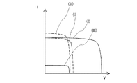
本形態では、上記実施の形態1で説明した光電変換装置100の特性について説明する。また、適宜、上述の特許文献1に示された3端子構造の太陽電池と比較して説明する。
本形態では、上記実施の形態で説明した図1の光電変換装置100と異なる構成について説明する。具体的には、第1のセル120の第2のセル140と対向する側の面に、濃度の異なる不純物半導体領域を設けたエミッタ構造の例を説明する。なお、図1と同じ構成については同じ符号を付し、詳細な説明は省略する。
上記実施の形態に示す光電変換装置は、さまざまな電子機器に用いることができる。なお、上記実施の形態に示す光電変換装置は、複数個を接続して集積化させて用いることもできる。本実施の形態では、一例として、電子書籍の電源として用いる例を説明する。
12 上部セル
14 下部セル
18 上部電極
24 絶縁膜
26 負極
28 正極
100 光電変換装置
105 絶縁層
107 第3の電極
109 透明導電膜
120 第1のセル
140 第2のセル
200 光電変換装置
230 絶縁層
101a 第1の電極
101b 第2の電極
121n 第1の不純物半導体領域
123p 第2の不純物半導体領域
125n 第3の不純物半導体層
127p 第4の不純物半導体層
141n 第5の不純物半導体層
143i 第6の半導体層
145p 第7の不純物半導体層
226p 第4の高濃度不純物半導体領域
227p 第4の低濃度不純物半導体領域
228p 第4の不純物半導体層
9000 電子書籍
9630 筐体
9631 表示部
9632 操作キー
9633 光電変換装置
9634 充放電制御回路
9635 バッテリー
9636 DCDCコンバータ
9637 DCDCコンバータ
Claims (7)
- 第1の光電変換層を含む第1のセルと、
前記第1のセルの一方の面と接し、且つ第2の光電変換層を含む第2のセルと、
前記第1のセルの他方の面側に設けられた、第1の電極及び第2の電極と、
前記第2のセルの、前記第1のセルと接する面と反対側の面に設けられた第3の電極と、を有し、
前記第2の光電変換層は、前記第1の光電変換層に含まれる第1の材料よりもバンドギャップが大きい第2の材料を含み、
前記第1のセル及び前記第2のセルが接する接触部は、pn接合が形成されており、
前記第1のセルは、第1のn型半導体層及び第1のp型半導体層を含む第2のn型半導体層と、第2のp型半導体層と、を有し、
前記第1のn型半導体層及び前記第1のp型半導体層は、前記第2のn型半導体層の一方の面側に設けられており、
前記第1のn型半導体層は、前記第1の電極と接する領域を有し、
前記第1のp型半導体層は、前記第2の電極と接する領域を有し、
前記第2のn型半導体層の他方の面は、前記第2のp型半導体層の一方の面と接し、
前記第2のp型半導体層の他方の面は、前記第2のセルと接し、
前記第1のn型半導体層と前記第1のp型半導体層とは、互いに分離されて設けられ、
前記第1の電極と前記第2の電極とは、互いに電気的に分離されており、
前記第2のセルは、前記第3の電極と電気的に接続されていることを特徴とする光電変換装置。 - 第1の光電変換層を含む第1のセルと、
第2の光電変換層を含む第2のセルと、
前記第1のセル及び前記第2のセルの間に設けられた、開口を有する絶縁層と、
前記第1のセルを挟んで前記開口を有する絶縁層と対向する前記第1のセルの一方の面側に設けられた、第1の電極及び第2の電極と、
前記第2のセルを挟んで前記開口を有する絶縁層と対向する前記第2のセルの一方の面側に設けられた、第3の電極と、を有し、
前記第2の光電変換層は、前記第1の光電変換層に含まれる第1の材料よりもバンドギャップが大きい第2の材料を含み、
前記第1のセルは、前記開口を介して前記第2のセルと接する領域を有し、
前記第1のセル及び前記第2のセルが接する接触部は、pn接合が形成されており、
前記第1のセルは、第1のn型半導体層及び第1のp型半導体層を含む第2のn型半導体層と、第2のp型半導体層と、を有し、
前記第1のn型半導体層及び前記第1のp型半導体層は、前記第2のn型半導体層の一方の面側に設けられており、
前記第1のn型半導体層は、前記第1の電極と接する領域を有し、
前記第1のp型半導体層は、前記第2の電極と接する領域を有し、
前記第2のn型半導体層の他方の面は、前記第2のp型半導体層の一方の面と接し、
前記第2のp型半導体層の他方の面は、前記第2のセルと接し、
前記第1のn型半導体層と前記第1のp型半導体層とは、互いに分離されて設けられ、
前記第1の電極と前記第2の電極とは、互いに電気的に分離されており、
前記第2のセルは、前記第3の電極と電気的に接続されていることを特徴とする光電変換装置。 - 請求項2において、
前記第2のp型半導体層は、第1の領域と、前記第1の領域の不純物濃度よりも高い不純物濃度を有する第2の領域と、を有することを特徴とする光電変換装置。 - 請求項3において、
前記第2の領域は、前記第2のセルと接するように設けられていることを特徴とする光電変換装置。 - 請求項1乃至4のいずれか一において、
前記第1のn型半導体層の不純物濃度は、前記第2のn型半導体層の不純物濃度よりも高いことを特徴とする光電変換装置。 - 請求項1乃至5のいずれか一において、
前記第1の材料は、単結晶シリコン又は多結晶シリコンであり、
前記第2の材料は、アモルファスシリコンであることを特徴とする光電変換装置。 - 請求項1乃至6のいずれか一において、
前記第2のセル及び前記第3の電極の間に設けられた透明導電膜を有することを特徴とする光電変換装置。
Priority Applications (1)
| Application Number | Priority Date | Filing Date | Title |
|---|---|---|---|
| JP2011132820A JP5753445B2 (ja) | 2010-06-18 | 2011-06-15 | 光電変換装置 |
Applications Claiming Priority (3)
| Application Number | Priority Date | Filing Date | Title |
|---|---|---|---|
| JP2010138889 | 2010-06-18 | ||
| JP2010138889 | 2010-06-18 | ||
| JP2011132820A JP5753445B2 (ja) | 2010-06-18 | 2011-06-15 | 光電変換装置 |
Publications (3)
| Publication Number | Publication Date |
|---|---|
| JP2012023351A JP2012023351A (ja) | 2012-02-02 |
| JP2012023351A5 JP2012023351A5 (ja) | 2014-06-26 |
| JP5753445B2 true JP5753445B2 (ja) | 2015-07-22 |
Family
ID=45327572
Family Applications (1)
| Application Number | Title | Priority Date | Filing Date |
|---|---|---|---|
| JP2011132820A Expired - Fee Related JP5753445B2 (ja) | 2010-06-18 | 2011-06-15 | 光電変換装置 |
Country Status (2)
| Country | Link |
|---|---|
| US (1) | US9048356B2 (ja) |
| JP (1) | JP5753445B2 (ja) |
Families Citing this family (3)
| Publication number | Priority date | Publication date | Assignee | Title |
|---|---|---|---|---|
| US10685983B2 (en) | 2016-11-11 | 2020-06-16 | Semiconductor Energy Laboratory Co., Ltd. | Transistor, semiconductor device, and electronic device |
| WO2020004475A1 (ja) * | 2018-06-29 | 2020-01-02 | 国立研究開発法人産業技術総合研究所 | 多接合光電変換素子及び多接合太陽電池 |
| JP6818208B1 (ja) * | 2020-08-01 | 2021-01-20 | 良昭 萩原 | 光電変換半導体装置 |
Family Cites Families (33)
| Publication number | Priority date | Publication date | Assignee | Title |
|---|---|---|---|---|
| US4272641A (en) * | 1979-04-19 | 1981-06-09 | Rca Corporation | Tandem junction amorphous silicon solar cells |
| US4316049A (en) | 1979-08-28 | 1982-02-16 | Rca Corporation | High voltage series connected tandem junction solar battery |
| US4496788A (en) | 1982-12-29 | 1985-01-29 | Osaka Transformer Co., Ltd. | Photovoltaic device |
| US4950614A (en) | 1984-05-15 | 1990-08-21 | Semiconductor Energy Laboratory Co., Ltd. | Method of making a tandem type semiconductor photoelectric conversion device |
| US4878097A (en) | 1984-05-15 | 1989-10-31 | Eastman Kodak Company | Semiconductor photoelectric conversion device and method for making same |
| US4680422A (en) | 1985-10-30 | 1987-07-14 | The Boeing Company | Two-terminal, thin film, tandem solar cells |
| US4684761A (en) | 1986-04-09 | 1987-08-04 | The Boeing Company | Method for making graded I-III-VI2 semiconductors and solar cell obtained thereby |
| JP3048732B2 (ja) | 1991-11-25 | 2000-06-05 | 三洋電機株式会社 | 光起電力装置 |
| US5656098A (en) | 1992-03-03 | 1997-08-12 | Canon Kabushiki Kaisha | Photovoltaic conversion device and method for producing same |
| US5248349A (en) | 1992-05-12 | 1993-09-28 | Solar Cells, Inc. | Process for making photovoltaic devices and resultant product |
| US5668050A (en) | 1994-04-28 | 1997-09-16 | Canon Kabushiki Kaisha | Solar cell manufacturing method |
| US6191353B1 (en) | 1996-01-10 | 2001-02-20 | Canon Kabushiki Kaisha | Solar cell module having a specific surface side cover excelling in moisture resistance and transparency |
| US5720827A (en) | 1996-07-19 | 1998-02-24 | University Of Florida | Design for the fabrication of high efficiency solar cells |
| JP3368822B2 (ja) * | 1998-03-19 | 2003-01-20 | トヨタ自動車株式会社 | 太陽電池 |
| JP3368854B2 (ja) * | 1998-12-25 | 2003-01-20 | トヨタ自動車株式会社 | 太陽電池 |
| US6166320A (en) * | 1998-03-19 | 2000-12-26 | Toyota Jidosha Kabushiki Kaisha | Tandem solar cell |
| JP2001160540A (ja) | 1999-09-22 | 2001-06-12 | Canon Inc | 半導体装置の製造方法、液相成長法及び液相成長装置、太陽電池 |
| KR100805210B1 (ko) | 2000-07-19 | 2008-02-21 | 마쯔시다덴기산교 가부시키가이샤 | 전극이 있는 기판 및 그 제조방법 |
| US6930025B2 (en) | 2001-02-01 | 2005-08-16 | Canon Kabushiki Kaisha | Transparent conductive film formation process, photovoltaic device production process, transparent conductive film, and photovoltaic device |
| JP4560245B2 (ja) | 2001-06-29 | 2010-10-13 | キヤノン株式会社 | 光起電力素子 |
| WO2006101200A1 (ja) * | 2005-03-24 | 2006-09-28 | Kyocera Corporation | 光電変換素子とその製造方法、及びこれを用いた光電変換モジュール |
| US7750425B2 (en) | 2005-12-16 | 2010-07-06 | The Trustees Of Princeton University | Intermediate-band photosensitive device with quantum dots embedded in energy fence barrier |
| TWI452703B (zh) | 2007-11-16 | 2014-09-11 | Semiconductor Energy Lab | 光電轉換裝置及其製造方法 |
| US20090139558A1 (en) | 2007-11-29 | 2009-06-04 | Shunpei Yamazaki | Photoelectric conversion device and manufacturing method thereof |
| EP2075850A3 (en) | 2007-12-28 | 2011-08-24 | Semiconductor Energy Laboratory Co, Ltd. | Photoelectric conversion device and manufacturing method thereof |
| EP2105972A3 (en) | 2008-03-28 | 2015-06-10 | Semiconductor Energy Laboratory Co, Ltd. | Photoelectric conversion device and method for manufacturing the same |
| US8338218B2 (en) | 2008-06-26 | 2012-12-25 | Semiconductor Energy Laboratory Co., Ltd. | Photoelectric conversion device module and manufacturing method of the photoelectric conversion device module |
| JP2010114299A (ja) * | 2008-11-07 | 2010-05-20 | Mitsubishi Heavy Ind Ltd | 光電変換装置の製造方法及び光電変換装置 |
| KR101732397B1 (ko) | 2009-06-05 | 2017-05-04 | 가부시키가이샤 한도오따이 에네루기 켄큐쇼 | 광전 변환 장치 및 그의 제작 방법 |
| CN102460722B (zh) | 2009-06-05 | 2015-04-01 | 株式会社半导体能源研究所 | 光电转换装置及其制造方法 |
| US8704083B2 (en) | 2010-02-11 | 2014-04-22 | Semiconductor Energy Laboratory Co., Ltd. | Photoelectric conversion device and fabrication method thereof |
| JP5792523B2 (ja) | 2010-06-18 | 2015-10-14 | 株式会社半導体エネルギー研究所 | 光電変換装置の作製方法 |
| US9076909B2 (en) | 2010-06-18 | 2015-07-07 | Semiconductor Energy Laboratory Co., Ltd. | Photoelectric conversion device and method for manufacturing the same |
-
2011
- 2011-06-15 JP JP2011132820A patent/JP5753445B2/ja not_active Expired - Fee Related
- 2011-06-17 US US13/163,091 patent/US9048356B2/en not_active Expired - Fee Related
Also Published As
| Publication number | Publication date |
|---|---|
| US20110308568A1 (en) | 2011-12-22 |
| JP2012023351A (ja) | 2012-02-02 |
| US9048356B2 (en) | 2015-06-02 |
Similar Documents
| Publication | Publication Date | Title |
|---|---|---|
| US8952244B2 (en) | Solar cell | |
| JP2011035092A (ja) | 裏面接合型太陽電池及びそれを用いた太陽電池モジュール | |
| KR20090059321A (ko) | 태양전지 | |
| WO2013055539A1 (en) | Photovoltaic devices and methods of forming the same | |
| US20120060890A1 (en) | Solar cell module and method for manufacturing the same | |
| KR20100009323A (ko) | 벌브 타입 집광형 태양전지 모듈 | |
| JP2006173381A (ja) | 光起電力素子 | |
| JP5753445B2 (ja) | 光電変換装置 | |
| KR20130016848A (ko) | Hit 태양전지 | |
| TWI506801B (zh) | 太陽能電池組 | |
| JP6706779B2 (ja) | 太陽電池および太陽電池モジュール | |
| KR20120086593A (ko) | 태양전지 및 그 제조방법 | |
| JP2012231142A (ja) | 太陽電池 | |
| JP2012038783A (ja) | 光電変換素子 | |
| JP2023033940A (ja) | 太陽電池セルおよび太陽電池 | |
| JP6000315B2 (ja) | 光起電力素子の製造方法 | |
| KR101531468B1 (ko) | 태양 전지 | |
| KR101667631B1 (ko) | 박막 태양전지 및 그의 제조 방법 | |
| US20160118514A1 (en) | Solar cell, solar cell panel, and solar cell film | |
| KR101898858B1 (ko) | 태양 전지 | |
| KR101325136B1 (ko) | 태양전지 | |
| CN115020519B (zh) | 一种太阳能叠层电池、电池组件和光伏系统 | |
| CN114883425B (zh) | 一种晶硅异质结太阳电池的迎光面结构 | |
| KR101562265B1 (ko) | 박막 태양전지 및 그 제조방법 | |
| JP2022143806A (ja) | 太陽電池セルおよび太陽電池 |
Legal Events
| Date | Code | Title | Description |
|---|---|---|---|
| A521 | Request for written amendment filed |
Free format text: JAPANESE INTERMEDIATE CODE: A523 Effective date: 20140509 |
|
| A621 | Written request for application examination |
Free format text: JAPANESE INTERMEDIATE CODE: A621 Effective date: 20140509 |
|
| A977 | Report on retrieval |
Free format text: JAPANESE INTERMEDIATE CODE: A971007 Effective date: 20141112 |
|
| A131 | Notification of reasons for refusal |
Free format text: JAPANESE INTERMEDIATE CODE: A131 Effective date: 20141118 |
|
| A521 | Request for written amendment filed |
Free format text: JAPANESE INTERMEDIATE CODE: A523 Effective date: 20141217 |
|
| TRDD | Decision of grant or rejection written | ||
| A01 | Written decision to grant a patent or to grant a registration (utility model) |
Free format text: JAPANESE INTERMEDIATE CODE: A01 Effective date: 20150512 |
|
| A61 | First payment of annual fees (during grant procedure) |
Free format text: JAPANESE INTERMEDIATE CODE: A61 Effective date: 20150522 |
|
| R150 | Certificate of patent or registration of utility model |
Ref document number: 5753445 Country of ref document: JP Free format text: JAPANESE INTERMEDIATE CODE: R150 |
|
| R250 | Receipt of annual fees |
Free format text: JAPANESE INTERMEDIATE CODE: R250 |
|
| R250 | Receipt of annual fees |
Free format text: JAPANESE INTERMEDIATE CODE: R250 |
|
| R250 | Receipt of annual fees |
Free format text: JAPANESE INTERMEDIATE CODE: R250 |
|
| R250 | Receipt of annual fees |
Free format text: JAPANESE INTERMEDIATE CODE: R250 |
|
| LAPS | Cancellation because of no payment of annual fees |