JP5721586B2 - 光学特性測定装置および光学特性測定方法 - Google Patents
光学特性測定装置および光学特性測定方法 Download PDFInfo
- Publication number
- JP5721586B2 JP5721586B2 JP2011176817A JP2011176817A JP5721586B2 JP 5721586 B2 JP5721586 B2 JP 5721586B2 JP 2011176817 A JP2011176817 A JP 2011176817A JP 2011176817 A JP2011176817 A JP 2011176817A JP 5721586 B2 JP5721586 B2 JP 5721586B2
- Authority
- JP
- Japan
- Prior art keywords
- film
- optical
- sample
- calculated
- light
- Prior art date
- Legal status (The legal status is an assumption and is not a legal conclusion. Google has not performed a legal analysis and makes no representation as to the accuracy of the status listed.)
- Active
Links
- 230000003287 optical effect Effects 0.000 title claims description 204
- 238000000034 method Methods 0.000 title claims description 30
- 238000005259 measurement Methods 0.000 claims description 87
- 239000000758 substrate Substances 0.000 claims description 37
- 230000014509 gene expression Effects 0.000 claims description 28
- 238000004458 analytical method Methods 0.000 claims description 20
- 238000004364 calculation method Methods 0.000 claims description 10
- 230000005540 biological transmission Effects 0.000 claims description 9
- 238000000691 measurement method Methods 0.000 claims description 9
- 239000000463 material Substances 0.000 claims description 7
- 238000002834 transmittance Methods 0.000 claims description 7
- 230000010287 polarization Effects 0.000 claims description 6
- 230000001678 irradiating effect Effects 0.000 claims 1
- 239000010408 film Substances 0.000 description 177
- 239000010410 layer Substances 0.000 description 50
- 238000012545 processing Methods 0.000 description 35
- 239000010409 thin film Substances 0.000 description 32
- 238000001228 spectrum Methods 0.000 description 28
- 238000000985 reflectance spectrum Methods 0.000 description 17
- 238000010586 diagram Methods 0.000 description 15
- 230000008033 biological extinction Effects 0.000 description 14
- 239000011347 resin Substances 0.000 description 11
- 229920005989 resin Polymers 0.000 description 11
- 230000003595 spectral effect Effects 0.000 description 9
- 238000001514 detection method Methods 0.000 description 8
- 230000008569 process Effects 0.000 description 6
- 230000008859 change Effects 0.000 description 5
- 239000002184 metal Substances 0.000 description 5
- 239000012528 membrane Substances 0.000 description 4
- 230000035945 sensitivity Effects 0.000 description 4
- YZCKVEUIGOORGS-OUBTZVSYSA-N Deuterium Chemical compound [2H] YZCKVEUIGOORGS-OUBTZVSYSA-N 0.000 description 3
- 229910052805 deuterium Inorganic materials 0.000 description 3
- 239000011521 glass Substances 0.000 description 3
- 230000007246 mechanism Effects 0.000 description 3
- 239000004065 semiconductor Substances 0.000 description 3
- 230000006870 function Effects 0.000 description 2
- 229910052736 halogen Inorganic materials 0.000 description 2
- 150000002367 halogens Chemical class 0.000 description 2
- 238000004519 manufacturing process Methods 0.000 description 2
- 239000013307 optical fiber Substances 0.000 description 2
- 230000001902 propagating effect Effects 0.000 description 2
- 229910052724 xenon Inorganic materials 0.000 description 2
- FHNFHKCVQCLJFQ-UHFFFAOYSA-N xenon atom Chemical compound [Xe] FHNFHKCVQCLJFQ-UHFFFAOYSA-N 0.000 description 2
- 230000000295 complement effect Effects 0.000 description 1
- 238000012790 confirmation Methods 0.000 description 1
- 230000004069 differentiation Effects 0.000 description 1
- 230000000694 effects Effects 0.000 description 1
- 238000003384 imaging method Methods 0.000 description 1
- 230000010354 integration Effects 0.000 description 1
- 239000004973 liquid crystal related substance Substances 0.000 description 1
- 239000011159 matrix material Substances 0.000 description 1
- 229910044991 metal oxide Inorganic materials 0.000 description 1
- 150000004706 metal oxides Chemical class 0.000 description 1
- 238000012986 modification Methods 0.000 description 1
- 230000004048 modification Effects 0.000 description 1
- 239000010453 quartz Substances 0.000 description 1
- 238000002310 reflectometry Methods 0.000 description 1
- 230000004044 response Effects 0.000 description 1
- 229910052594 sapphire Inorganic materials 0.000 description 1
- 239000010980 sapphire Substances 0.000 description 1
- VYPSYNLAJGMNEJ-UHFFFAOYSA-N silicon dioxide Inorganic materials O=[Si]=O VYPSYNLAJGMNEJ-UHFFFAOYSA-N 0.000 description 1
- 239000002356 single layer Substances 0.000 description 1
Images


Classifications
-
- G—PHYSICS
- G01—MEASURING; TESTING
- G01B—MEASURING LENGTH, THICKNESS OR SIMILAR LINEAR DIMENSIONS; MEASURING ANGLES; MEASURING AREAS; MEASURING IRREGULARITIES OF SURFACES OR CONTOURS
- G01B11/00—Measuring arrangements characterised by the use of optical techniques
- G01B11/02—Measuring arrangements characterised by the use of optical techniques for measuring length, width or thickness
- G01B11/06—Measuring arrangements characterised by the use of optical techniques for measuring length, width or thickness for measuring thickness ; e.g. of sheet material
- G01B11/0616—Measuring arrangements characterised by the use of optical techniques for measuring length, width or thickness for measuring thickness ; e.g. of sheet material of coating
- G01B11/0625—Measuring arrangements characterised by the use of optical techniques for measuring length, width or thickness for measuring thickness ; e.g. of sheet material of coating with measurement of absorption or reflection
-
- G—PHYSICS
- G01—MEASURING; TESTING
- G01B—MEASURING LENGTH, THICKNESS OR SIMILAR LINEAR DIMENSIONS; MEASURING ANGLES; MEASURING AREAS; MEASURING IRREGULARITIES OF SURFACES OR CONTOURS
- G01B11/00—Measuring arrangements characterised by the use of optical techniques
- G01B11/02—Measuring arrangements characterised by the use of optical techniques for measuring length, width or thickness
- G01B11/06—Measuring arrangements characterised by the use of optical techniques for measuring length, width or thickness for measuring thickness ; e.g. of sheet material
- G01B11/0616—Measuring arrangements characterised by the use of optical techniques for measuring length, width or thickness for measuring thickness ; e.g. of sheet material of coating
- G01B11/0641—Measuring arrangements characterised by the use of optical techniques for measuring length, width or thickness for measuring thickness ; e.g. of sheet material of coating with measurement of polarization
-
- G—PHYSICS
- G01—MEASURING; TESTING
- G01N—INVESTIGATING OR ANALYSING MATERIALS BY DETERMINING THEIR CHEMICAL OR PHYSICAL PROPERTIES
- G01N21/00—Investigating or analysing materials by the use of optical means, i.e. using sub-millimetre waves, infrared, visible or ultraviolet light
- G01N21/17—Systems in which incident light is modified in accordance with the properties of the material investigated
- G01N21/21—Polarisation-affecting properties
- G01N21/211—Ellipsometry
- G01N2021/213—Spectrometric ellipsometry
Description
好ましくは、波長分布特性から算出するパラメータは、膜の反射率または透過率である。
<装置構成>
図1は、本発明の実施の形態1に従う光学特性測定装置100の概略構成図である。
図2は、本発明の実施の形態1に従うデータ処理部50の概略のハードウェア構成を示す模式図である。
本実施の形態1に従うデータ処理部50が、試料を構成する膜の膜厚および光学定数を測定するために、検出器40によって取得された反射率スペクトルに対して行なう演算処理について説明する。
膜モデル式を説明する前に、まず、試料に測定光を照射した場合に観測される反射光について、数学的および物理的に検討を行う。

式(2)〜式(5)を用いて、雰囲気層、薄膜層、基板層の3層からなる試料OBJにおける偏光のP成分,S成分の複素反射係数RP,RSは、式(6)と表わすことができる。
また、Forouhi-Bloomerモデルを用いて光学定数を表わした膜モデル式は、式(9)のように表わすことができる。
図3に戻って、モデル化部501は、測定点ごとに取得したスペクトルから、測定点ごとに膜モデル式を生成する。たとえば、1枚の基板から5点測定する場合や、5枚の基板のそれぞれに対して1点測定する場合、モデル化部501は、測定点ごとに取得した5つのスペクトルから、測定点ごとに5つの膜モデル式を生成する。
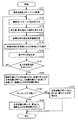
次に、フローチャートを参照して、本発明の実施の形態1に従う光学特性測定方法について説明する。
それぞれ算出される。
<装置構成>
図12は、本発明の実施の形態2に従う光学特性測定装置110の概略構成図である。
次に、フローチャートを参照して、本発明の実施の形態2に従う光学特性測定方法について説明する。
Claims (6)
- 基板上に少なくとも1層の膜を形成した被測定物に対して所定の波長範囲をもつ測定光を照射する光源と、
前記被測定物で反射された光または前記被測定物を透過した光に基づいて、反射強度または透過強度の波長分布特性を取得する分光測定部と、
同一材料の前記膜から複数の前記波長分布特性を取得し、取得した各々の前記波長分布特性から算出するパラメータと、前記膜の膜厚および光学定数とを少なくとも含む複数の膜モデル式を生成するモデル化部と、
前記モデル化部で生成した複数の前記膜モデル式を連立させ、複数の前記膜モデル式に含まれる前記光学定数が同一であるとして所定の演算を行ない、前記膜の前記膜厚および前記光学定数を算出する解析部と、
前記解析部で算出した前記膜の前記膜厚および前記光学定数を前記膜モデル式に代入して得られる波形と、前記分光測定部で取得した前記波長分布特性の波形とのフィッティングを行なうことにより、複数の前記膜モデル式に含まれる前記光学定数が同一で、前記解析部で算出した前記膜の前記膜厚および前記光学定数が正しい値であることを判定するフィッティング部と
を備える光学特性測定装置。 - 前記解析部は、前記所定の演算に非線形最小二乗法を用いる、請求項1に記載の光学特性測定装置。
- 前記波長分布特性から算出する前記パラメータは、前記膜の反射率または透過率である、請求項1または請求項2に記載の光学特性測定装置。
- 前記分光測定部は、前記被測定物で反射された光に基づいて、偏光反射強度の前記波長分布特性を取得し、
前記波長分布特性から算出する前記パラメータは、位相差Δおよび振幅比Ψである、請求項1または請求項2に記載の光学特性測定装置。 - 前記モデル化部は、前記膜の裏面反射係数寄与率をさらに含む前記膜モデル式を生成する、請求項1〜請求項4のいずれか1項に記載の光学特性測定装置。
- 基板上に少なくとも1層の膜を形成した被測定物に対して所定の波長範囲をもつ測定光を照射し、
前記被測定物で反射された光または前記被測定物を透過した光に基づいて、反射強度または透過強度の波長分布特性を、同一材料の前記膜から複数取得し、
取得した各々の前記波長分布特性から算出するパラメータと、前記膜の光学定数とを含む複数の膜モデル式を生成し、
生成した複数の前記膜モデル式を連立させ、複数の前記膜モデル式に含まれる前記光学定数が同一であるとして所定の演算を行ない、前記膜の膜厚および前記光学定数を算出し、
算出した前記膜の前記膜厚および前記光学定数を前記膜モデル式に代入して得られる波形と、取得した前記波長分布特性の波形とのフィッティングを行なうことにより、複数の前記膜モデル式に含まれる前記光学定数が同一で、算出した前記膜の前記膜厚および前記光学定数が正しい値であることを判定する、光学特性測定方法。
Priority Applications (5)
| Application Number | Priority Date | Filing Date | Title |
|---|---|---|---|
| JP2011176817A JP5721586B2 (ja) | 2011-08-12 | 2011-08-12 | 光学特性測定装置および光学特性測定方法 |
| TW101124166A TWI540306B (zh) | 2011-08-12 | 2012-07-05 | 光學特性測量裝置及光學特性測量方法 |
| US13/548,210 US8582124B2 (en) | 2011-08-12 | 2012-07-13 | Optical characteristic measuring apparatus and optical characteristic measuring method |
| KR1020120087386A KR101841776B1 (ko) | 2011-08-12 | 2012-08-09 | 광학 특성 측정 장치 및 광학 특성 측정 방법 |
| CN201210285463.8A CN102954765B (zh) | 2011-08-12 | 2012-08-10 | 光学特性测量装置以及光学特性测量方法 |
Applications Claiming Priority (1)
| Application Number | Priority Date | Filing Date | Title |
|---|---|---|---|
| JP2011176817A JP5721586B2 (ja) | 2011-08-12 | 2011-08-12 | 光学特性測定装置および光学特性測定方法 |
Publications (3)
| Publication Number | Publication Date |
|---|---|
| JP2013040813A JP2013040813A (ja) | 2013-02-28 |
| JP2013040813A5 JP2013040813A5 (ja) | 2014-08-14 |
| JP5721586B2 true JP5721586B2 (ja) | 2015-05-20 |
Family
ID=47677359
Family Applications (1)
| Application Number | Title | Priority Date | Filing Date |
|---|---|---|---|
| JP2011176817A Active JP5721586B2 (ja) | 2011-08-12 | 2011-08-12 | 光学特性測定装置および光学特性測定方法 |
Country Status (5)
| Country | Link |
|---|---|
| US (1) | US8582124B2 (ja) |
| JP (1) | JP5721586B2 (ja) |
| KR (1) | KR101841776B1 (ja) |
| CN (1) | CN102954765B (ja) |
| TW (1) | TWI540306B (ja) |
Families Citing this family (33)
| Publication number | Priority date | Publication date | Assignee | Title |
|---|---|---|---|---|
| JP5834584B2 (ja) * | 2011-07-25 | 2015-12-24 | ソニー株式会社 | 情報処理装置、情報処理方法、プログラム及び蛍光スペクトルの強度補正方法 |
| JP5721586B2 (ja) * | 2011-08-12 | 2015-05-20 | 大塚電子株式会社 | 光学特性測定装置および光学特性測定方法 |
| US8830464B2 (en) * | 2012-11-06 | 2014-09-09 | Kla-Tencor Corporation | Film thickness, refractive index, and extinction coefficient determination for film curve creation and defect sizing in real time |
| CN103217387B (zh) * | 2013-03-22 | 2015-04-15 | 清华大学 | 测量金属氧化层高温光学常数的方法 |
| CN103712568B (zh) * | 2013-12-11 | 2016-05-04 | 浙江工商大学 | 一种基于机器视觉的塑料托盘反光特征检测系统 |
| CN103680276B (zh) * | 2014-01-08 | 2016-06-08 | 黄河科技学院 | 一种验证光电效应实验规律及测定普朗克常数的实验装置 |
| JP2015152835A (ja) * | 2014-02-17 | 2015-08-24 | キヤノン株式会社 | 波長選択偏光素子、光学系および投射型表示装置 |
| KR102254033B1 (ko) | 2014-06-13 | 2021-05-20 | 삼성전자주식회사 | 광학 측정 방법 및 광학 측정 시스템 |
| CN104111235B (zh) * | 2014-07-11 | 2016-10-05 | 北京大学 | 一种测量二维薄膜材料复折射率谱的方法 |
| CN104502282B (zh) * | 2015-01-21 | 2017-03-01 | 哈尔滨工业大学 | 考虑光子晶体表面氧化膜分布的偏振特性数值计算方法 |
| CN105674899B (zh) * | 2016-01-26 | 2019-03-19 | 国家纳米科学中心 | 一种采用光谱椭偏仪对金属膜进行检测的方法 |
| US10438825B2 (en) * | 2016-08-29 | 2019-10-08 | Kla-Tencor Corporation | Spectral reflectometry for in-situ process monitoring and control |
| CN106814048B (zh) * | 2017-01-18 | 2018-04-17 | 湖南大学 | 一种从气凝胶玻璃实验数据反推气凝胶消光系数的方法 |
| JP2018128326A (ja) * | 2017-02-07 | 2018-08-16 | 大塚電子株式会社 | 光学スペクトル測定装置および光学スペクトル測定方法 |
| JP6285597B1 (ja) * | 2017-06-05 | 2018-02-28 | 大塚電子株式会社 | 光学測定装置および光学測定方法 |
| JP2019020419A (ja) * | 2017-07-20 | 2019-02-07 | Jfeテクノリサーチ株式会社 | 膜厚計算方法、膜厚計算プログラム及び膜厚計算装置 |
| US10663286B2 (en) * | 2017-08-22 | 2020-05-26 | Kla-Tencor Corporation | Measuring thin films on grating and bandgap on grating |
| CN107576615B (zh) * | 2017-09-25 | 2020-09-29 | 国家纳米科学中心 | 一种纳米线吸收谱的测量方法及系统 |
| CN109750450B (zh) * | 2017-11-01 | 2022-03-04 | 青岛海尔智能技术研发有限公司 | 一种识别衣物材质的智能模块及智能洗衣机 |
| JP6402273B1 (ja) * | 2018-05-18 | 2018-10-10 | 大塚電子株式会社 | 光学測定装置及び光学測定方法 |
| JP7103159B2 (ja) * | 2018-10-29 | 2022-07-20 | コニカミノルタ株式会社 | 光学特性評価方法及び光学特性評価システム |
| CN109596532A (zh) * | 2018-12-14 | 2019-04-09 | 天津津航技术物理研究所 | 一种光学基底材料光学常数的测试方法 |
| CN109883553B (zh) * | 2019-03-14 | 2020-01-21 | 上海精测半导体技术有限公司 | 一种偏振测量装置及偏振测量方法 |
| CN110108200B (zh) * | 2019-04-28 | 2021-02-09 | 北京卫星制造厂有限公司 | 一种基于改进枝切法的激光散斑相位解包裹方法 |
| JP7300332B2 (ja) * | 2019-07-04 | 2023-06-29 | シャープ株式会社 | 多層膜形成体の評価装置および評価方法 |
| CN111337227B (zh) * | 2020-04-30 | 2022-05-10 | 宜昌南玻显示器件有限公司 | 一种基于vba的基板光学常数计算方法 |
| CN112362593A (zh) * | 2020-11-18 | 2021-02-12 | 华侨大学 | 金刚石衬底随温度变化的测量方法 |
| CN112557345B (zh) * | 2020-11-30 | 2022-03-11 | 华中科技大学 | 一种物体成分均匀性的测定装置和测定方法 |
| CN113267454A (zh) * | 2021-05-26 | 2021-08-17 | 中国工程物理研究院激光聚变研究中心 | 薄膜品质检测方法、装置、电子设备及存储介质 |
| JP2023042311A (ja) * | 2021-09-14 | 2023-03-27 | 東京エレクトロン株式会社 | 基板処理装置、基板処理方法及び記憶媒体 |
| CN113959387A (zh) * | 2021-11-24 | 2022-01-21 | 威海华菱光电股份有限公司 | 裂缝测量装置 |
| CN116124017B (zh) * | 2023-01-06 | 2024-03-22 | 深圳市埃芯半导体科技有限公司 | 薄膜膜厚的测量方法、装置、电子设备及存储介质 |
| CN117109643B (zh) * | 2023-10-24 | 2024-01-02 | 中国科学院长春光学精密机械与物理研究所 | 应用透射式角度传感器件的测试方法及系统 |
Family Cites Families (14)
| Publication number | Priority date | Publication date | Assignee | Title |
|---|---|---|---|---|
| US5835226A (en) | 1997-11-13 | 1998-11-10 | Lsi Logic Corporation | Method for determining optical constants prior to film processing to be used improve accuracy of post-processing thickness measurements |
| US6836324B2 (en) * | 1998-03-18 | 2004-12-28 | Nova Measuring Instruments Ltd. | Method and apparatus for measurements of patterned structures |
| JP3790628B2 (ja) | 1998-08-20 | 2006-06-28 | 大塚電子株式会社 | 膜厚及び光学定数の測定方法及び装置 |
| JP3817094B2 (ja) * | 1999-07-09 | 2006-08-30 | シャープ株式会社 | 薄膜の膜厚測定装置 |
| JP3852557B2 (ja) * | 2000-09-08 | 2006-11-29 | オムロン株式会社 | 膜厚測定方法およびその方法を用いた膜厚センサ |
| US7196782B2 (en) * | 2000-09-20 | 2007-03-27 | Kla-Tencor Technologies Corp. | Methods and systems for determining a thin film characteristic and an electrical property of a specimen |
| US6940592B2 (en) * | 2001-10-09 | 2005-09-06 | Applied Materials, Inc. | Calibration as well as measurement on the same workpiece during fabrication |
| JP3995579B2 (ja) | 2002-10-18 | 2007-10-24 | 大日本スクリーン製造株式会社 | 膜厚測定装置および反射率測定装置 |
| KR101193830B1 (ko) * | 2004-08-09 | 2012-10-23 | 가부시키가이샤 니콘 | 광학 특성 계측 장치 및 광학 특성 계측 방법, 노광 장치및 노광 방법, 그리고 디바이스 제조 방법 |
| JP2007040930A (ja) * | 2005-08-05 | 2007-02-15 | Ebara Corp | 膜厚測定方法及び基板処理装置 |
| JP5302631B2 (ja) * | 2008-11-08 | 2013-10-02 | 株式会社堀場製作所 | 光学測定装置、プログラム、及び計測方法 |
| CN101762891B (zh) * | 2008-12-23 | 2011-12-28 | 财团法人工业技术研究院 | 液晶单元的光学特性测量系统及其方法 |
| JP2010169667A (ja) * | 2008-12-26 | 2010-08-05 | Tokyo Electron Ltd | 金属膜の膜厚測定方法及び基板処理方法及び装置 |
| JP5721586B2 (ja) * | 2011-08-12 | 2015-05-20 | 大塚電子株式会社 | 光学特性測定装置および光学特性測定方法 |
-
2011
- 2011-08-12 JP JP2011176817A patent/JP5721586B2/ja active Active
-
2012
- 2012-07-05 TW TW101124166A patent/TWI540306B/zh active
- 2012-07-13 US US13/548,210 patent/US8582124B2/en active Active
- 2012-08-09 KR KR1020120087386A patent/KR101841776B1/ko active IP Right Grant
- 2012-08-10 CN CN201210285463.8A patent/CN102954765B/zh active Active
Also Published As
| Publication number | Publication date |
|---|---|
| US20130038883A1 (en) | 2013-02-14 |
| KR101841776B1 (ko) | 2018-03-23 |
| CN102954765A (zh) | 2013-03-06 |
| JP2013040813A (ja) | 2013-02-28 |
| CN102954765B (zh) | 2016-12-21 |
| TWI540306B (zh) | 2016-07-01 |
| TW201317541A (zh) | 2013-05-01 |
| US8582124B2 (en) | 2013-11-12 |
| KR20130018164A (ko) | 2013-02-20 |
Similar Documents
| Publication | Publication Date | Title |
|---|---|---|
| JP5721586B2 (ja) | 光学特性測定装置および光学特性測定方法 | |
| JP6830492B2 (ja) | 分光ビームプロファイルオーバーレイ計測 | |
| US10365163B2 (en) | Optical critical dimension metrology | |
| CN102636963B (zh) | 检查设备和方法、光刻设备和处理单元、器件制造方法 | |
| TWI360653B (en) | Inspection method and apparatus, lithographic appa | |
| KR101582357B1 (ko) | 막 두께 측정 장치 및 막 두께 측정 방법 | |
| JP5382792B2 (ja) | 光2次非線形薄膜における1次及び2次光感受率異方性同時測定方法、当該方法を実行する装置及び当該方法をコンピュータに実行させるプログラム | |
| KR101509054B1 (ko) | 광소자-회전형 뮬러-행렬 타원계측기 및 이를 이용한 시료의 뮬러-행렬 측정 방법 | |
| CN107003114A (zh) | 光谱光束轮廓计量 | |
| KR20050091997A (ko) | 측정 방법, 해석 방법, 측정 장치, 해석 장치, 엘립소미터및 컴퓨터 프로그램 | |
| JP4834847B2 (ja) | 多層膜解析装置および多層膜解析方法 | |
| TWI460413B (zh) | 測量樣品特性之方法與裝置以及非過渡性電腦可讀媒體 | |
| JP2010002328A (ja) | 膜厚測定装置 | |
| JP3520379B2 (ja) | 光学定数測定方法およびその装置 | |
| KR101424840B1 (ko) | 광탄성 측정방법 및 그 장치 | |
| US20230266233A1 (en) | System for measuring thickness and physical properties of thin film using spatial light modulator | |
| TW202001999A (zh) | 半導體生產期間之製程誘導位移表徵 | |
| JP2009047685A (ja) | 光弾性測定方法およびその装置 | |
| JP2003240526A (ja) | 表面測定装置及びその測定方法 | |
| JP5028660B2 (ja) | 光学特性測定装置および光学特性測定方法 | |
| KR100870132B1 (ko) | 음향광학 변조 필터를 이용한 분광타원해석기 및 이를이용한 타원 해석방법 | |
| CN107314839A (zh) | 基于穆勒矩阵的应力检测装置及方法 | |
| JP4715199B2 (ja) | 膜厚測定装置及び膜厚測定方法 | |
| JP2005201634A (ja) | 膜厚測定方法、及び装置 | |
| KR20090105288A (ko) | 칼라필터를 이용한 3차원 두께와 형상 동시 측정장치 및 그측정방법 |
Legal Events
| Date | Code | Title | Description |
|---|---|---|---|
| A521 | Request for written amendment filed |
Free format text: JAPANESE INTERMEDIATE CODE: A523 Effective date: 20140702 |
|
| A621 | Written request for application examination |
Free format text: JAPANESE INTERMEDIATE CODE: A621 Effective date: 20140702 |
|
| A977 | Report on retrieval |
Free format text: JAPANESE INTERMEDIATE CODE: A971007 Effective date: 20150305 |
|
| TRDD | Decision of grant or rejection written | ||
| A01 | Written decision to grant a patent or to grant a registration (utility model) |
Free format text: JAPANESE INTERMEDIATE CODE: A01 Effective date: 20150317 |
|
| A61 | First payment of annual fees (during grant procedure) |
Free format text: JAPANESE INTERMEDIATE CODE: A61 Effective date: 20150324 |
|
| R150 | Certificate of patent or registration of utility model |
Ref document number: 5721586 Country of ref document: JP Free format text: JAPANESE INTERMEDIATE CODE: R150 |
|
| R250 | Receipt of annual fees |
Free format text: JAPANESE INTERMEDIATE CODE: R250 |
|
| R250 | Receipt of annual fees |
Free format text: JAPANESE INTERMEDIATE CODE: R250 |
|
| R250 | Receipt of annual fees |
Free format text: JAPANESE INTERMEDIATE CODE: R250 |
|
| R250 | Receipt of annual fees |
Free format text: JAPANESE INTERMEDIATE CODE: R250 |
|
| R250 | Receipt of annual fees |
Free format text: JAPANESE INTERMEDIATE CODE: R250 |
|
| R250 | Receipt of annual fees |
Free format text: JAPANESE INTERMEDIATE CODE: R250 |
|
| R250 | Receipt of annual fees |
Free format text: JAPANESE INTERMEDIATE CODE: R250 |