JP5714664B2 - Lighting device - Google Patents
Lighting device Download PDFInfo
- Publication number
- JP5714664B2 JP5714664B2 JP2013152572A JP2013152572A JP5714664B2 JP 5714664 B2 JP5714664 B2 JP 5714664B2 JP 2013152572 A JP2013152572 A JP 2013152572A JP 2013152572 A JP2013152572 A JP 2013152572A JP 5714664 B2 JP5714664 B2 JP 5714664B2
- Authority
- JP
- Japan
- Prior art keywords
- radiator
- lighting device
- antenna element
- terminal
- light source
- Prior art date
- Legal status (The legal status is an assumption and is not a legal conclusion. Google has not performed a legal analysis and makes no representation as to the accuracy of the status listed.)
- Active
Links
- 230000008878 coupling Effects 0.000 claims description 58
- 238000010168 coupling process Methods 0.000 claims description 58
- 238000005859 coupling reaction Methods 0.000 claims description 58
- 238000004891 communication Methods 0.000 claims description 40
- 239000000758 substrate Substances 0.000 claims description 36
- 230000001681 protective effect Effects 0.000 claims description 32
- 238000003780 insertion Methods 0.000 claims description 20
- 230000037431 insertion Effects 0.000 claims description 20
- 230000017525 heat dissipation Effects 0.000 claims description 7
- 230000000903 blocking effect Effects 0.000 description 15
- 230000004308 accommodation Effects 0.000 description 8
- 239000000463 material Substances 0.000 description 5
- -1 polypropylene Polymers 0.000 description 4
- PXHVJJICTQNCMI-UHFFFAOYSA-N Nickel Chemical compound [Ni] PXHVJJICTQNCMI-UHFFFAOYSA-N 0.000 description 3
- KDLHZDBZIXYQEI-UHFFFAOYSA-N Palladium Chemical compound [Pd] KDLHZDBZIXYQEI-UHFFFAOYSA-N 0.000 description 3
- 238000006243 chemical reaction Methods 0.000 description 3
- 239000004020 conductor Substances 0.000 description 3
- BASFCYQUMIYNBI-UHFFFAOYSA-N platinum Chemical compound [Pt] BASFCYQUMIYNBI-UHFFFAOYSA-N 0.000 description 3
- 239000004698 Polyethylene Substances 0.000 description 2
- 239000004743 Polypropylene Substances 0.000 description 2
- 239000010949 copper Substances 0.000 description 2
- 239000010931 gold Substances 0.000 description 2
- 238000005286 illumination Methods 0.000 description 2
- 238000009413 insulation Methods 0.000 description 2
- 239000003973 paint Substances 0.000 description 2
- 239000004033 plastic Substances 0.000 description 2
- 229920003023 plastic Polymers 0.000 description 2
- 229920000515 polycarbonate Polymers 0.000 description 2
- 239000004417 polycarbonate Substances 0.000 description 2
- 229920000573 polyethylene Polymers 0.000 description 2
- 229920001155 polypropylene Polymers 0.000 description 2
- 230000005855 radiation Effects 0.000 description 2
- 239000011347 resin Substances 0.000 description 2
- 229920005989 resin Polymers 0.000 description 2
- RYGMFSIKBFXOCR-UHFFFAOYSA-N Copper Chemical compound [Cu] RYGMFSIKBFXOCR-UHFFFAOYSA-N 0.000 description 1
- BQCADISMDOOEFD-UHFFFAOYSA-N Silver Chemical compound [Ag] BQCADISMDOOEFD-UHFFFAOYSA-N 0.000 description 1
- 229910052802 copper Inorganic materials 0.000 description 1
- 230000007613 environmental effect Effects 0.000 description 1
- 239000011521 glass Substances 0.000 description 1
- PCHJSUWPFVWCPO-UHFFFAOYSA-N gold Chemical compound [Au] PCHJSUWPFVWCPO-UHFFFAOYSA-N 0.000 description 1
- 229910052737 gold Inorganic materials 0.000 description 1
- 239000012212 insulator Substances 0.000 description 1
- 238000000034 method Methods 0.000 description 1
- 229910052759 nickel Inorganic materials 0.000 description 1
- 229910052763 palladium Inorganic materials 0.000 description 1
- 229910052697 platinum Inorganic materials 0.000 description 1
- 238000000926 separation method Methods 0.000 description 1
- 229910052709 silver Inorganic materials 0.000 description 1
- 239000004332 silver Substances 0.000 description 1
Images


Classifications
-
- F—MECHANICAL ENGINEERING; LIGHTING; HEATING; WEAPONS; BLASTING
- F21—LIGHTING
- F21V—FUNCTIONAL FEATURES OR DETAILS OF LIGHTING DEVICES OR SYSTEMS THEREOF; STRUCTURAL COMBINATIONS OF LIGHTING DEVICES WITH OTHER ARTICLES, NOT OTHERWISE PROVIDED FOR
- F21V23/00—Arrangement of electric circuit elements in or on lighting devices
- F21V23/04—Arrangement of electric circuit elements in or on lighting devices the elements being switches
- F21V23/0435—Arrangement of electric circuit elements in or on lighting devices the elements being switches activated by remote control means
-
- F—MECHANICAL ENGINEERING; LIGHTING; HEATING; WEAPONS; BLASTING
- F21—LIGHTING
- F21V—FUNCTIONAL FEATURES OR DETAILS OF LIGHTING DEVICES OR SYSTEMS THEREOF; STRUCTURAL COMBINATIONS OF LIGHTING DEVICES WITH OTHER ARTICLES, NOT OTHERWISE PROVIDED FOR
- F21V33/00—Structural combinations of lighting devices with other articles, not otherwise provided for
-
- F—MECHANICAL ENGINEERING; LIGHTING; HEATING; WEAPONS; BLASTING
- F21—LIGHTING
- F21K—NON-ELECTRIC LIGHT SOURCES USING LUMINESCENCE; LIGHT SOURCES USING ELECTROCHEMILUMINESCENCE; LIGHT SOURCES USING CHARGES OF COMBUSTIBLE MATERIAL; LIGHT SOURCES USING SEMICONDUCTOR DEVICES AS LIGHT-GENERATING ELEMENTS; LIGHT SOURCES NOT OTHERWISE PROVIDED FOR
- F21K9/00—Light sources using semiconductor devices as light-generating elements, e.g. using light-emitting diodes [LED] or lasers
- F21K9/20—Light sources comprising attachment means
- F21K9/23—Retrofit light sources for lighting devices with a single fitting for each light source, e.g. for substitution of incandescent lamps with bayonet or threaded fittings
- F21K9/232—Retrofit light sources for lighting devices with a single fitting for each light source, e.g. for substitution of incandescent lamps with bayonet or threaded fittings specially adapted for generating an essentially omnidirectional light distribution, e.g. with a glass bulb
-
- F—MECHANICAL ENGINEERING; LIGHTING; HEATING; WEAPONS; BLASTING
- F21—LIGHTING
- F21V—FUNCTIONAL FEATURES OR DETAILS OF LIGHTING DEVICES OR SYSTEMS THEREOF; STRUCTURAL COMBINATIONS OF LIGHTING DEVICES WITH OTHER ARTICLES, NOT OTHERWISE PROVIDED FOR
- F21V15/00—Protecting lighting devices from damage
- F21V15/01—Housings, e.g. material or assembling of housing parts
-
- F—MECHANICAL ENGINEERING; LIGHTING; HEATING; WEAPONS; BLASTING
- F21—LIGHTING
- F21V—FUNCTIONAL FEATURES OR DETAILS OF LIGHTING DEVICES OR SYSTEMS THEREOF; STRUCTURAL COMBINATIONS OF LIGHTING DEVICES WITH OTHER ARTICLES, NOT OTHERWISE PROVIDED FOR
- F21V17/00—Fastening of component parts of lighting devices, e.g. shades, globes, refractors, reflectors, filters, screens, grids or protective cages
- F21V17/10—Fastening of component parts of lighting devices, e.g. shades, globes, refractors, reflectors, filters, screens, grids or protective cages characterised by specific fastening means or way of fastening
- F21V17/12—Fastening of component parts of lighting devices, e.g. shades, globes, refractors, reflectors, filters, screens, grids or protective cages characterised by specific fastening means or way of fastening by screwing
-
- F—MECHANICAL ENGINEERING; LIGHTING; HEATING; WEAPONS; BLASTING
- F21—LIGHTING
- F21V—FUNCTIONAL FEATURES OR DETAILS OF LIGHTING DEVICES OR SYSTEMS THEREOF; STRUCTURAL COMBINATIONS OF LIGHTING DEVICES WITH OTHER ARTICLES, NOT OTHERWISE PROVIDED FOR
- F21V29/00—Protecting lighting devices from thermal damage; Cooling or heating arrangements specially adapted for lighting devices or systems
- F21V29/50—Cooling arrangements
- F21V29/70—Cooling arrangements characterised by passive heat-dissipating elements, e.g. heat-sinks
- F21V29/74—Cooling arrangements characterised by passive heat-dissipating elements, e.g. heat-sinks with fins or blades
- F21V29/77—Cooling arrangements characterised by passive heat-dissipating elements, e.g. heat-sinks with fins or blades with essentially identical diverging planar fins or blades, e.g. with fan-like or star-like cross-section
- F21V29/773—Cooling arrangements characterised by passive heat-dissipating elements, e.g. heat-sinks with fins or blades with essentially identical diverging planar fins or blades, e.g. with fan-like or star-like cross-section the planes containing the fins or blades having the direction of the light emitting axis
-
- F—MECHANICAL ENGINEERING; LIGHTING; HEATING; WEAPONS; BLASTING
- F21—LIGHTING
- F21V—FUNCTIONAL FEATURES OR DETAILS OF LIGHTING DEVICES OR SYSTEMS THEREOF; STRUCTURAL COMBINATIONS OF LIGHTING DEVICES WITH OTHER ARTICLES, NOT OTHERWISE PROVIDED FOR
- F21V29/00—Protecting lighting devices from thermal damage; Cooling or heating arrangements specially adapted for lighting devices or systems
- F21V29/50—Cooling arrangements
- F21V29/70—Cooling arrangements characterised by passive heat-dissipating elements, e.g. heat-sinks
- F21V29/74—Cooling arrangements characterised by passive heat-dissipating elements, e.g. heat-sinks with fins or blades
- F21V29/77—Cooling arrangements characterised by passive heat-dissipating elements, e.g. heat-sinks with fins or blades with essentially identical diverging planar fins or blades, e.g. with fan-like or star-like cross-section
- F21V29/777—Cooling arrangements characterised by passive heat-dissipating elements, e.g. heat-sinks with fins or blades with essentially identical diverging planar fins or blades, e.g. with fan-like or star-like cross-section the planes containing the fins or blades having directions perpendicular to the light emitting axis
-
- H—ELECTRICITY
- H05—ELECTRIC TECHNIQUES NOT OTHERWISE PROVIDED FOR
- H05B—ELECTRIC HEATING; ELECTRIC LIGHT SOURCES NOT OTHERWISE PROVIDED FOR; CIRCUIT ARRANGEMENTS FOR ELECTRIC LIGHT SOURCES, IN GENERAL
- H05B47/00—Circuit arrangements for operating light sources in general, i.e. where the type of light source is not relevant
- H05B47/10—Controlling the light source
- H05B47/175—Controlling the light source by remote control
- H05B47/19—Controlling the light source by remote control via wireless transmission
-
- F—MECHANICAL ENGINEERING; LIGHTING; HEATING; WEAPONS; BLASTING
- F21—LIGHTING
- F21Y—INDEXING SCHEME ASSOCIATED WITH SUBCLASSES F21K, F21L, F21S and F21V, RELATING TO THE FORM OR THE KIND OF THE LIGHT SOURCES OR OF THE COLOUR OF THE LIGHT EMITTED
- F21Y2115/00—Light-generating elements of semiconductor light sources
- F21Y2115/10—Light-emitting diodes [LED]
-
- H—ELECTRICITY
- H05—ELECTRIC TECHNIQUES NOT OTHERWISE PROVIDED FOR
- H05B—ELECTRIC HEATING; ELECTRIC LIGHT SOURCES NOT OTHERWISE PROVIDED FOR; CIRCUIT ARRANGEMENTS FOR ELECTRIC LIGHT SOURCES, IN GENERAL
- H05B45/00—Circuit arrangements for operating light-emitting diodes [LED]
- H05B45/30—Driver circuits
- H05B45/37—Converter circuits
-
- Y—GENERAL TAGGING OF NEW TECHNOLOGICAL DEVELOPMENTS; GENERAL TAGGING OF CROSS-SECTIONAL TECHNOLOGIES SPANNING OVER SEVERAL SECTIONS OF THE IPC; TECHNICAL SUBJECTS COVERED BY FORMER USPC CROSS-REFERENCE ART COLLECTIONS [XRACs] AND DIGESTS
- Y02—TECHNOLOGIES OR APPLICATIONS FOR MITIGATION OR ADAPTATION AGAINST CLIMATE CHANGE
- Y02B—CLIMATE CHANGE MITIGATION TECHNOLOGIES RELATED TO BUILDINGS, e.g. HOUSING, HOUSE APPLIANCES OR RELATED END-USER APPLICATIONS
- Y02B20/00—Energy efficient lighting technologies, e.g. halogen lamps or gas discharge lamps
- Y02B20/30—Semiconductor lamps, e.g. solid state lamps [SSL] light emitting diodes [LED] or organic LED [OLED]
Landscapes
- Engineering & Computer Science (AREA)
- General Engineering & Computer Science (AREA)
- Computer Networks & Wireless Communication (AREA)
- Physics & Mathematics (AREA)
- Microelectronics & Electronic Packaging (AREA)
- Optics & Photonics (AREA)
- Non-Portable Lighting Devices Or Systems Thereof (AREA)
- Arrangement Of Elements, Cooling, Sealing, Or The Like Of Lighting Devices (AREA)
Description
本発明は、照明装置に関する。 The present invention relates to a lighting device.
一般に、照明装置は、用途に応じて、天井直付灯、景観照明灯、就寝灯、スタンドなど、様々な形態で提供されている。このような照明装置は、目的によって、十分な輝度レベルで点灯しなければならない。このために、近年、照明装置に、発光ダイオード(LED)が利用されている。発光ダイオードは、蛍光灯、白熱灯のような既存の光源と比較して、低消費電力、半永久的な寿命、早い応答速度、安全性、環境親和性のメリットを有する。そのため、既存の光源を発光ダイオードに代替するための研究が進められている。 In general, lighting devices are provided in various forms such as a direct ceiling light, a landscape lighting, a sleeping lamp, and a stand depending on the application. Such an illuminating device must be lit at a sufficient luminance level depending on the purpose. For this reason, in recent years, light emitting diodes (LEDs) have been used in lighting devices. Light emitting diodes have the advantages of low power consumption, semi-permanent lifetime, fast response speed, safety, and environmental compatibility compared with existing light sources such as fluorescent lamps and incandescent lamps. Therefore, research for replacing the existing light source with a light emitting diode is underway.
ところが、上記のような照明装置は、有線で接続されたスイッチによって、オン/オフされる。このため、照明装置の使用者には、照明装置を制御することに煩わしさがあった。 However, the lighting device as described above is turned on / off by a switch connected by wire. For this reason, the user of the illuminating device has been troublesome to control the illuminating device.
したがって、本発明の目的は、容易に制御可能な照明装置を提供することにある。 Accordingly, an object of the present invention is to provide an illumination device that can be easily controlled.
課題を解決するための本発明による照明装置は、電力を供給する制御モジュールと、制御モジュールを収容する放熱体と、放熱体に装着され、制御モジュールに接続される光源と、放熱体に挿入され、制御モジュールに接続される接続端子、及び放熱体から突出するアンテナ素子を有する通信モジュールと、を含むことを特徴とする。 A lighting device according to the present invention for solving the problem includes a control module that supplies power, a heat radiating body that houses the control module, a light source that is attached to the heat radiating body and is connected to the control module, and is inserted into the heat radiating body. And a communication module having a connection terminal connected to the control module and an antenna element protruding from the radiator.
本発明による照明装置は、無線通信機能を有する。このとき、照明装置は、通信モジュールを介して、無線制御信号を受信することができる。そして、照明装置は、無線制御信号によって、光源を制御することができる。これによって、照明装置の無線制御が可能である。すなわち、照明装置の使用者が照明装置を容易に制御することができる。これによって、照明装置を使用する使用者の便宜性が向上する。 The lighting device according to the present invention has a wireless communication function. At this time, the lighting device can receive a wireless control signal via the communication module. And the illuminating device can control a light source with a wireless control signal. This enables wireless control of the lighting device. That is, the user of the lighting device can easily control the lighting device. This improves the convenience of the user who uses the lighting device.
以下、添付の図面を参照して、本発明の実施例をより詳しく説明する。添付の図面において、同一の構成要素は、できるだけ、同一の符号で示していることに留意されたい。そして、本発明の要旨を不明確にするような公知機能及び構成に対する詳細な説明は、省略する。 Hereinafter, embodiments of the present invention will be described in detail with reference to the accompanying drawings. It should be noted that in the accompanying drawings, the same components are denoted by the same reference numerals as much as possible. Detailed descriptions of known functions and configurations that obscure the gist of the present invention will be omitted.
下記の説明において、それぞれの構成要素が別の構成要素の「上」、又は「下」に形成されると記載された場合、「上」及び「下」は、「直接」又は「他の構成要素を介して(indirectly)」形成されることをすべて含む。また、それぞれの構成要素の上又は下に対する基準は、図面の上下を基準として説明する。 In the following description, when it is stated that each component is formed “above” or “below” another component, “above” and “below” are “direct” or “other configurations”. Includes everything formed "indirectly". In addition, the reference to the top or bottom of each component will be described with reference to the top and bottom of the drawing.
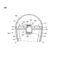
図1は、本発明の実施例による照明装置を分解して示す斜視図であり、図2は、本発明の実施例による照明装置の結合構造を示す斜視図である。そして、図3は、図1において、通信モジュールを分解して示す斜視図である。また、図4は、図1において、А-А’に沿って切断した断面を示す断面図である。 FIG. 1 is an exploded perspective view illustrating a lighting device according to an embodiment of the present invention, and FIG. 2 is a perspective view illustrating a coupling structure of the lighting device according to the embodiment of the present invention. FIG. 3 is an exploded perspective view showing the communication module in FIG. 4 is a cross-sectional view showing a cross section taken along А-А 'in FIG.
図1〜図4を参照すると、本実施例の照明装置100は、光源110と、光源結合部120と、背光カバーと、制御モジュール140と、ハウジング150と、遮断カバー160と、給電カバー170と、放熱体180と、通信モジュール190とを含む。
1 to 4, the
光源110は、光を発生する。ここで、光源110は、発光ダイオードであってよい。このような光源110は、給電素子111と、複数の給電ワイヤ113と、複数のベース基板115と、複数の発光ダイオード素子117とを含む。
The
給電素子111は、光源110から電力を供給する。ここで、給電素子111は、印刷回路基板(PCB)であってよい。
The
給電ワイヤ113は、給電素子111とベース基板115とを接続する。このとき、給電ワイヤ113は、給電素子111とそれぞれのベース基板115とを直接接続することができる。又は、給電ワイヤ113は、給電素子111とベース基板115の一部とを接続し、ベース基板115を相互接続することができる。そして、給電ワイヤ113は、給電素子111からベース基板115に電力を伝達する。
The
ベース基板115は、光源110の駆動を制御する。このとき、ベース基板115は、発光ダイオードに給電素子111の電力を印加する。ここで、ベース基板115は、印刷回路基板であってよい。
The
発光ダイオード素子117は、ベース基板115に実装される。このとき、それぞれのベース基板115に、複数の発光ダイオード素子117が実装することができる。そして、発光ダイオード素子117は、ベース基板115から印加される電力によって、光を発生させる。すなわち、発光ダイオード素子117が、光を出力する。
The light
光源結合部120は、光源110に結合されて、光源110を固定する。このとき、光源結合部120に、少なくとも1つの第1の結合孔121と、少なくとも1つの第2の結合孔123とが形成されている。第1の結合孔121は、ベース基板115を収容する。ここで、光源結合部120は、ベース基板115と発光ダイオード素子117とを、第1の結合孔121の位置で固定する。そして、光源結合部120は、第1の結合孔121を介して、発光ダイオード素子117を露出させる。また、第2の結合孔123は、給電素子111と通信モジュール190とを収容する。さらに、光源結合部120は、第2の結合孔123を介して、給電素子111及び通信モジュール190を露出させる。ここで、第2の結合孔123は、通信モジュール190を通過させる。つまり、第2の結合孔123は、光源結合部120を境界に、両方向に通信モジュール190を突出させる。ここで、光源結合部120は、絶縁体で形成してもよい。
The light
背光カバーは、光源結合部120の上で光源110を囲む。ここで、背光カバーは、開口部が形成されたバルブ状を有してもよい。そして、背光カバーは、光源110を保護し、光源110の光を放出する。このとき、背光カバーは、照明装置100の前面又は背面に配光する。ここで、背光カバーは、ガラス、プラスチック、ポリプロピレン、ポリエチレンの少なくともいずれか一つによって形成することができる。又は、背光カバーは、耐光性、耐熱性、衝撃強度特性に優れるポリカーボネートで形成してもよい。また、背光カバーにおいて、光源110に対向する内部面に、乳白色塗料がコーティングされていることがある。塗料は、光を拡散するための拡散材を含んでもよい。
The back cover surrounds the
制御モジュール140は、照明装置100の全般的な動作を制御する。このとき、図示されてはいないが、制御モジュール140は、主基板及び複数の部品を含むことができる。主基板は、印刷回路基板であってよい。部品は、主基板に実装されて、主基板に電気的に接続される。これらの部品は、変換部及び駆動部を含む。変換部は、主基板を介して、外部電源に接続される。そして、変換部は、外部電源の交流電源を直流電源に変換する。駆動部は、光源110の駆動を制御する。
The
そして、制御モジュール140は、光源110に電力を供給する。ここで、制御モジュール140は、電源供給装置(PSU)であってよい。このとき、制御モジュール140は、通信モジュール190から受信される無線制御信号によって、光源110を制御することができる。このような制御モジュール140は、給電端子141と、結合端子143とを含む。
The
給電端子141は、光源110と接続される。このような給電端子141は、光源110の給電素子111と接触する。このとき、給電端子141は、制御モジュール140から突出する。ここで、給電端子141は、主基板に結合され、主基板から突出する。そして、給電端子141は、給電素子111に対向する。
The
そして、給電端子141は、光源110に電力を供給する。すなわち、制御モジュール140は、給電素子111を介して、光源110に電力を供給する。また、給電端子141は、光源110に、光源110を制御するための光源制御信号を送信する。すなわち、制御モジュール140は、給電素子111を介して、光源110に光源制御信号を伝達する。
The
結合端子143は、通信モジュール190と接続される。このような結合端子143は、通信モジュール190と結合される。このとき、結合端子143は、制御モジュール140から突出してもよい。ここで、結合端子143は、主基板に結合され、主基板から突出する。そして、結合端子143は、通信モジュール190を収容することができる。ここで、結合端子143に、結合溝145を形成してもよい。結合溝145は、通信モジュール190に対向してもよい。また、結合溝145が、通信モジュール190を収容してもよい。
The
ハウジング150は、制御モジュール140を収容する。このようなハウジング150に、収容孔151が形成されている。すなわち、ハウジング150は、収容孔151によって、制御モジュール140を収容する。このとき、ハウジング150は、円筒状に形成してもよい。そして、ハウジング150は、制御モジュール140と放熱体180との間の電気的ショートを防止することができる。ここで、ハウジング150は、絶縁性及び耐久性に優れる材質で形成してもよい。また、ハウジング150は、樹脂材質で形成してもよい。
The
そして、ハウジング150は、接続端子153を含む。このとき、ハウジング150は、接続端子153を介して、外部電源に固定される。ここで、接続端子153は、ソケット方式で外部電源に固定してもよい。また、接続端子153は、外部電源に接続することができる。すなわち、接続端子153は、外部電源に電気的に接続することができる。さらに、接続端子153は、制御モジュール140と外部電源とを電気的に接続することができる。ここで、接続端子153は、導電性物質で作られていてもよい。
The
遮断カバー160は、ハウジング150を封止する。このような遮断カバー160は、ハウジング150の収容孔151を上から覆う。このとき、遮断カバー160は、制御モジュール140と放熱体180との間の電気的ショートを防止することができる。ここで、遮断カバー160は、絶縁性及び耐久性に優れる材質で形成してもよい。また、遮断カバー160は、樹脂材質で形成してもよい。
The blocking
そして、遮断カバー160に、少なくとも1つの貫通孔161が形成されている。貫通孔161は、第2の結合孔123と同一軸上に配置される。そして、貫通孔161は、給電端子141と通信モジュール190とを収容する。このとき、貫通孔161は、給電端子141と通信モジュール190とを通過させる。ここで、遮断カバー160は、貫通孔161を介して、給電端子141と結合端子143とを露出させる。すなわち、貫通孔161は、給電素子111に向けて給電端子141を突出させる。また、貫通孔161は、結合端子143に向けて通信モジュール190を突出させる。
In addition, at least one through
給電カバー170は、ハウジング150を封止する。このような給電カバー170は、ハウジング150の収容孔を下から覆う。そして、給電カバー170は、外部電源に接触する。このとき、給電カバー170は、制御モジュール140と外部電源とを電気的に接続する。ここで、給電カバー170は、導電性物質で作られていてもよい。
The
放熱体180は、制御モジュール140、ハウジング150、及び遮断カバー160を収容する。このような放熱体180に、収容溝(図示せず)が形成されている。すなわち、放熱体180は、収容溝によって、制御モジュール140、ハウジング150、及び遮断カバー160を収容する。そして、放熱体180に、光源110が装着される。また、放熱体180は、光源110で発生される熱を放散させ、光源110で発生される熱から制御モジュール140を保護する。このとき、放熱体180は、第1の放熱体181と第2の放熱体185とを含む。
The
第1の放熱体181は、遮断カバー160の上に配置される。このような第1の放熱体181は、背光カバーと結合される。このとき、第1の放熱体181は、縁部で背光カバーに固定される。そして、第1の放熱体181の上に、光源110と、光源結合部120とが装着される。このような第1の放熱体181は、光源110と接触する。このとき、第1の放熱体181は、光源110で発生される熱を、第2の放熱体185に移動させる。ここで、第1の放熱体181は、円形に形成される。また、第1の放熱体181は、平面に形成することができる。
The first
そして、第1の放熱体181に、少なくとも1つの挿入孔183が形成されている。挿入孔183は、第2の結合孔123及び貫通孔161と同一軸上に配置される。そして、挿入孔183は、給電端子141と通信モジュール190とを収容する。このとき、挿入孔183は、給電端子141と通信モジュール190とを通過させる。ここで、第1の放熱体181は、挿入孔183を介して、給電端子141と結合端子143とを露出させる。すなわち、挿入孔183は、給電素子111に向けて給電端子141を突出させる。また、挿入孔183は、結合端子143に向けて通信モジュール190を突出させる。
In addition, at least one
第2の放熱体185は、ハウジング150を取り囲む。このとき、第2の放熱体185は、接続端子153を露出させる。つまり、第2の放熱体185は、ハウジング150において、接続端子153を除く部分を取り囲む。ここで、第2の放熱体185は、円筒状に形成することができる。このような第2の放熱体185は、第1の放熱体181から下へ延在する。このとき、第2の放熱体185は、光源110で発生する熱を放散させる。ここで、第2の放熱体185は、第1の放熱体181の中心軸に沿って、下に延在するほど、直径が減少してもよい。
The
そして、第2の放熱体185は、複数の放熱ピン187を含む。このとき、第2の放熱体185が放熱ピン187を含むことによって、表面積が増加する。放熱ピン187は、第1の放熱体181から下へ延在する。このとき、放熱ピン187は、第1の放熱体181の中心軸から放射状に配置してもよい。ここで、放熱ピン187は、第1の放熱体181の中心軸に垂直な方向に突出する。
The second
通信モジュール190は、照明装置100の制御のための無線制御信号を受信する。このとき、通信モジュール190は、制御モジュール140に接続する。ここで、通信モジュール190は、光源110と離隔し、光源結合部120、放熱体180、及び遮断カバー160を横切る。そして、通信モジュール190は、制御モジュール140に結合される。このような通信モジュール190は、基板210と、接続端子220と、接地部230と、アンテナ素子240と、保護カバー250とを含む。
The
基板210は、通信モジュール190において、支持のために設けられる。このとき、基板210は、平板構造を有する。ここで、基板210は、印刷回路基板であってよい。そして、基板210は、誘電体を含むことができる。このような基板210は、接続領域211と、駆動領域213と、アンテナ領域215とを含む。
The
接続領域211は、基板210の一端部に位置する。このような接続領域211は、制御モジュール140に対向する。このとき、接続領域211は、結合端子143に対向する。ここで、接続領域211は、結合溝145に対向してもよい。そして、接続領域211は、放熱体180に挿入される。このとき、接続領域211は、放熱体180の収容溝に収容される。また、接続領域211は、制御モジュール140に結合される。このとき、接続領域211は、結合端子143に固定される。ここで、接続領域211は、結合溝145に挿入することができる。
The
駆動領域213は、接続領域211から延在する。このとき、駆動領域213は、基板210の中央に位置する。このような駆動領域213は、光源結合部120、放熱体180、及び遮断カバー160を横切る。そして、駆動領域213は、放熱体180に挿入される。このとき、駆動領域213は、同一軸上の第2の結合孔123、挿入孔183、貫通孔161、及び放熱体180の収容溝に収容される。
The
そして、駆動領域213は、駆動素子(図示せず)を含む。このとき、駆動素子は、基板210に内在し、駆動領域213に配置される。ここで、駆動素子は、駆動領域213から延在する。また、駆動素子の一端部は、接続領域211に延在し、他端部は、アンテナ領域215に延在する。
The
アンテナ領域215は、基板210において他端部に位置する。ここで、アンテナ領域215は、駆動領域213を境界に、接続領域211の反対側に位置する。そして、アンテナ領域215は、駆動領域213を介して、接続領域211に接続される。このようなアンテナ領域215は、放熱体180から突出する。ここで、アンテナ領域215は、放熱体180から露出する。このとき、アンテナ領域215は、光源結合部120の上に位置する。ここで、アンテナ領域215は、光源110から離隔してもよい。
The
接続端子220は、通信モジュール190において、制御モジュール140とのインターフェースのために設けられる。このような接続端子220は、基板210の接続領域211に配置される。このとき、接続端子220は、駆動素子の一端部に接続される。そして、接続端子220は、制御モジュール140に接続される。このとき、接続端子220は、接続領域211と共に結合端子143に固定されて、結合端子143に接続する。ここで、接続端子220は、結合溝145に挿入することができる。また、接続端子220を介して、通信モジュール190に電力が供給される。すなわち、結合端子143から接続端子220に、電力が供給される。
The
接地部230は、通信モジュール190において、接地のために設けられる。このような接地部230は、基板210の接続領域211に配置される。このとき、接地部230は、接続端子220から離隔してもよい。すなわち、接地部230は、接続端子220に接触しないようにしてもよい。そして、接地部230は、駆動素子の一端部に接続することができる。
The
アンテナ素子240は、通信モジュール190において、無線通信機能を提供する。このとき、アンテナ素子240は、所定の周波数帯域で共振し、電磁波を送受信する。ここで、アンテナ素子240は、所定のインピーダンスで共振する。このようなアンテナ素子240は、基板210のアンテナ領域215に配置される。このとき、アンテナ素子240は、駆動素子の他端部に接続される。すなわち、アンテナ素子240は、駆動素子を介して、接続端子220に接続される。ここで、アンテナ素子240は、駆動素子を介して、接地部230に接続してもよい。そして、アンテナ素子240の一端部が駆動素子に接続され、他端部が開放される。
The
そして、アンテナ素子240は、放熱体180から突出する。ここで、アンテナ素子240は、放熱体180の外部に配置される。すなわち、アンテナ素子240は、アンテナ領域215と共に放熱体180から露出する。また、アンテナ素子240は、放熱体180から離隔する。ここで、アンテナ素子240と放熱体180との離隔距離(d)は、略1mm以上である。このとき、アンテナ素子240は、光源結合部120の上に位置する。ここで、アンテナ素子240は、光源110から離隔してもよい。
The
また、アンテナ素子240は、接続端子220から供給される電力を用いて、駆動する。このとき、アンテナ素子240は、制御モジュール140を制御するための無線制御信号を受信する。そして、アンテナ素子240は、無線制御信号を制御モジュール140に送信する。このとき、アンテナ素子240は、接続端子220を介して、制御モジュール140に無線制御信号を送信する。
The
このとき、アンテナ素子240は、パッチタイプで形成された後、アンテナ領域215に取り付けられる。又は、アンテナ素子240は、導電性インクで線描することによって、アンテナ領域215に形成される。又は、アンテナ素子240は、アンテナ領域215に柄出し(patterning)してもよい。ここで、アンテナ素子240は、バー(bar)形、ミアンダ形、らせん形、階段形、又はループ形の少なくともいずれか一つで形成することができる。そして、アンテナ素子240は、導電性物質で作成してもよい。ここで、アンテナ素子240は、銀(Ag)、パラジウム(Pd)、白金(Pt)、銅(Cu)、金(Au)、ニッケル(Ni)の少なくともいずれか一つを含むことができる。
At this time, the
保護カバー250は、基板210を収容する。このとき、保護カバー250は、基板210を覆う。ここで、保護カバー250は、駆動領域213とアンテナ領域215とを覆い、接続領域211を露出させる。すなわち、保護カバー250は、アンテナ素子240を収容し、接続端子220を露出させる。言い換えると、接続端子220が、保護カバー250から突出する。ここで、保護カバー250は、プラスチック、ポリプロピレン、ポリエチレン、ポリカーボネートの少なくともいずれか一つで形成することができる。このような保護カバー250は、第1の保護カバー251と、第2の保護カバー253とを含む。
The
第1の保護カバー251は、駆動領域213を取り囲む。このような第1の保護カバー251は、駆動領域213と共に、光源結合部120、放熱体180、及び遮断カバー160を横切る。そして、第1の保護カバー251は、放熱体180に挿入される。このとき、第1の保護カバー251は、同一軸上の第2の結合孔123、挿入孔183、貫通孔161、及び放熱体180の収容溝に収容される。
The first
第2の保護カバー253は、アンテナ領域215を収容する。そして、第2の保護カバー253は、アンテナ素子240を収容する。ここで、第2の保護カバー253は、第1の保護カバー251から延在する。このとき、第2の保護カバー253に、挿入溝が形成されている。つまり、第2の保護カバー253は、挿入溝を介して、アンテナ領域215と共に、アンテナ素子240を収容する。
The second
そして、第2の保護カバー253は、放熱体180から突出する。ここで、第2の保護カバー253は、放熱体180から露出する。このとき、第2の保護カバー253は、アンテナ素子240を放熱体180から離隔する。ここで、第2の保護カバー253は、光源結合部120の上に位置する。また、第2の保護カバー253は、放熱体180に固定される。このとき、第2の保護カバー253は、放熱体180に挿入しないように、挿入孔183よりも大きいサイズで形成される。
The second
本発明によると、照明装置100は、無線通信機能を有する。このとき、照明装置100は、通信モジュール190を介して、無線制御信号を受信することができる。そして、照明装置100は、無線制御信号によって、光源110を制御することができる。これによって、照明装置100の無線制御が可能である。すなわち、照明装置100を使用する使用者が、照明装置100を容易に制御することができる。これによって、照明装置100を使用する使用者の便宜性が向上する。
According to the present invention, the
本明細書と図面に開示している本発明の実施例は、本発明の技術内容を容易に説明し、本発明の理解を助けるために、特定の例を提示したことに過ぎず、本発明の範囲を限定することではない。すなわち、本発明の技術的思想に基づく他の変形例が実施可能であるということは、本発明が属する技術の分野における通常の知識を有する者にとって、自明なことである。 The embodiments of the present invention disclosed in this specification and the drawings are merely provided as specific examples in order to easily explain the technical contents of the present invention and to help understand the present invention. It is not meant to limit the range. That is, it is obvious to those having ordinary knowledge in the technical field to which the present invention pertains that other variations based on the technical idea of the present invention can be implemented.
100 照明装置
110 光源
111、141 給電素子
113 給電ワイヤ
115 ベース基板
117 発光ダイオード素子
120 光源結合部
121、123 結合孔
140 制御モジュール
143 結合端子
145 結合溝
150 ハウジング
153 接続端子
160 遮断カバー
161 貫通孔
170 給電カバー
180、181、185 放熱体
183 挿入孔
187 放熱ピン
190 通信モジュール
210 基板
211 接続領域
220 接続端子
230 接地部
240 アンテナ素子
250、251、253 保護カバー
DESCRIPTION OF
Claims (9)
前記放熱体の収容空間の内に収容され、前記放熱体に形成された第1挿入孔を介して前記放熱体の外部に露出する結合端子を有する制御モジュールと、
前記放熱体の上面の上に装着され、前記制御モジュールに接続される光源と、
前記放熱体の第1挿入孔を介して前記放熱体の収容空間の内部に挿入され、前記制御モジュールの結合端子と直接接続する接続端子、及び前記放熱体の上面から突出するアンテナ素子を有する通信モジュールと、を含み、
前記接続端子は、前記結合端子の内部に挿入され、前記結合端子と電気的に結合される、照明装置。 A radiator having an accommodating space inside and having a first insertion hole formed on the upper surface;
A control module having a coupling terminal that is accommodated in an accommodating space of the radiator and exposed to the outside of the radiator through a first insertion hole formed in the radiator;
A light source mounted on the upper surface of the radiator and connected to the control module;
Communication having a connection terminal that is inserted into the space of the heat dissipation body through the first insertion hole of the heat dissipation body and directly connected to the coupling terminal of the control module, and an antenna element protruding from the upper surface of the heat dissipation body includes a module, the,
The connection terminal is inserted into the coupling terminal and electrically coupled to the coupling terminal .
前記接続端子が配置される接続領域と、
前記アンテナ素子が配置されるアンテナ領域と、
前記接続領域とアンテナ領域との間に介在し、前記駆動素子が配置される駆動領域と、
を含むことを特徴とする、請求項6に記載の照明装置。 The substrate is
A connection region in which the connection terminals are disposed;
An antenna region in which the antenna element is disposed;
A drive region that is interposed between the connection region and the antenna region and in which the drive element is disposed;
The lighting device according to claim 6, comprising:
前記放熱体に挿入される第1の保護カバーと、
前記放熱体に固定され、前記放熱体から突出する第2の保護カバーと、を含み、
前記保護カバーの幅は、前記第1挿入孔の幅より大きいことを特徴とする、請求項5乃至7のいずれか一項に記載の照明装置。 The protective cover is
A first protective cover inserted into the radiator;
Fixed to said heat radiator, seen including a second protective cover projecting from the radiator,
The lighting device according to claim 5 , wherein a width of the protective cover is larger than a width of the first insertion hole .
前記制御モジュールには、前記第2挿入孔に挿入される給電端子を含み、
前記給電端子は、
前記第2挿入孔を介して前記放熱体の外部に露出し、前記光源の給電素子と直接接触することを特徴とする、請求項1乃至8のいずれか一項に記載の照明装置。 A second insertion hole is formed on the upper surface of the radiator,
The control module includes a power supply terminal inserted into the second insertion hole,
The power supply terminal is
9. The lighting device according to claim 1 , wherein the lighting device is exposed to the outside of the heat radiating body through the second insertion hole and is in direct contact with a power feeding element of the light source .
Applications Claiming Priority (2)
| Application Number | Priority Date | Filing Date | Title |
|---|---|---|---|
| KR10-2012-0079877 | 2012-07-23 | ||
| KR1020120079877A KR101360678B1 (en) | 2012-07-23 | 2012-07-23 | Lighting apparatus |
Related Child Applications (1)
| Application Number | Title | Priority Date | Filing Date |
|---|---|---|---|
| JP2015046680A Division JP6334437B2 (en) | 2012-07-23 | 2015-03-10 | Lighting device |
Publications (2)
| Publication Number | Publication Date |
|---|---|
| JP2014022376A JP2014022376A (en) | 2014-02-03 |
| JP5714664B2 true JP5714664B2 (en) | 2015-05-07 |
Family
ID=48875539
Family Applications (2)
| Application Number | Title | Priority Date | Filing Date |
|---|---|---|---|
| JP2013152572A Active JP5714664B2 (en) | 2012-07-23 | 2013-07-23 | Lighting device |
| JP2015046680A Active JP6334437B2 (en) | 2012-07-23 | 2015-03-10 | Lighting device |
Family Applications After (1)
| Application Number | Title | Priority Date | Filing Date |
|---|---|---|---|
| JP2015046680A Active JP6334437B2 (en) | 2012-07-23 | 2015-03-10 | Lighting device |
Country Status (4)
| Country | Link |
|---|---|
| US (3) | US9253859B2 (en) |
| EP (2) | EP2690359B1 (en) |
| JP (2) | JP5714664B2 (en) |
| KR (1) | KR101360678B1 (en) |
Families Citing this family (41)
| Publication number | Priority date | Publication date | Assignee | Title |
|---|---|---|---|---|
| US9488324B2 (en) * | 2011-09-02 | 2016-11-08 | Soraa, Inc. | Accessories for LED lamp systems |
| WO2013142733A1 (en) | 2012-03-21 | 2013-09-26 | Greene Charles E | Wireless sensor system, method and apparatus with switch and outlet control |
| US11221110B2 (en) * | 2013-03-13 | 2022-01-11 | Smartbotics, Inc. | LED light bulb construction and manufacture |
| JP6235698B2 (en) | 2013-04-23 | 2017-11-22 | フィリップス ライティング ホールディング ビー ヴィ | Lighting device and antenna including antenna |
| WO2015057556A1 (en) | 2013-10-15 | 2015-04-23 | LIFI Labs, Inc. | Lighting assembly |
| CN105766067B (en) * | 2013-10-23 | 2019-06-18 | 鲍尔卡斯特公司 | Automatic system for Lighting control |
| US11455884B2 (en) | 2014-09-02 | 2022-09-27 | LIFI Labs, Inc. | Lighting system |
| EP3069575B1 (en) | 2013-11-14 | 2018-09-26 | Lifi Labs Inc. | Resettable lighting system and method |
| KR20150109656A (en) * | 2014-03-20 | 2015-10-02 | 엘지이노텍 주식회사 | Lighting apparatus |
| US9538623B2 (en) | 2014-05-12 | 2017-01-03 | Lg Electronics Inc. | Lighting device |
| US9435521B2 (en) | 2014-05-21 | 2016-09-06 | Technical Consumer Products, Inc. | Antenna element for a directional lighting fixture |
| EP3146254B1 (en) | 2014-05-22 | 2020-04-22 | Lifi Labs Inc. | Directional lighting system and method |
| US9488352B2 (en) * | 2014-05-28 | 2016-11-08 | Technical Consumer Products, Inc. | Radio frequency (RF) signal pathway for a lamp antenna |
| US9210773B1 (en) | 2014-05-29 | 2015-12-08 | Technical Consumer Products, Inc. | Wireless light fixture |
| JP6473925B2 (en) * | 2014-09-11 | 2019-02-27 | パナソニックIpマネジメント株式会社 | lighting equipment |
| US9949348B2 (en) * | 2014-11-10 | 2018-04-17 | LIFI Labs, Inc. | Lighting connectivity module |
| JP6969592B2 (en) * | 2015-01-21 | 2021-11-24 | 三菱電機株式会社 | lighting equipment |
| JP6263318B1 (en) * | 2015-03-17 | 2018-01-17 | フィリップス ライティング ホールディング ビー ヴィ | Illumination apparatus comprising first and second antennas coupled and movable relative to each other |
| CA2983910C (en) * | 2015-04-27 | 2023-09-26 | Osram Sylvania Inc. | Wireless mounted control module |
| JP6579511B2 (en) * | 2015-05-11 | 2019-09-25 | パナソニックIpマネジメント株式会社 | Light source unit and lighting fixture equipped with the same |
| US10317018B2 (en) * | 2015-09-01 | 2019-06-11 | Lg Innotek Co., Ltd. | Lighting device |
| CN109891937B (en) | 2016-10-07 | 2023-07-18 | 鲍尔卡斯特公司 | Lighting control automation system |
| US10440794B2 (en) | 2016-11-02 | 2019-10-08 | LIFI Labs, Inc. | Lighting system and method |
| JP2018137113A (en) * | 2017-02-21 | 2018-08-30 | パナソニックIpマネジメント株式会社 | Lighting device and light fitting |
| BE1026104B1 (en) * | 2018-03-16 | 2019-10-14 | Schreder S.A. | CONNECTED LUMINAIRE |
| CN112204813B (en) * | 2018-05-31 | 2024-05-17 | 昕诺飞控股有限公司 | Stacked circuit board in lighting device |
| EP3824696B1 (en) | 2018-07-16 | 2022-09-07 | Signify Holding B.V. | A lighting device and a method |
| CN108944653B (en) * | 2018-09-14 | 2024-05-14 | 常州瑞阳电装有限公司 | Global type flash drive circuit |
| CN209130543U (en) * | 2018-11-13 | 2019-07-19 | 漳州立达信光电子科技有限公司 | A kind of intelligent lamp |
| CN109511207B (en) * | 2019-01-09 | 2024-07-02 | 苏州蓝石新动力有限公司 | Lamplight synchronization method and system |
| US10935228B2 (en) | 2019-04-03 | 2021-03-02 | Lutron Technology Company Llc | Wireless controllable lighting device |
| JP6840188B2 (en) * | 2019-05-07 | 2021-03-10 | 三菱電機株式会社 | lighting equipment |
| CN211625172U (en) * | 2020-01-16 | 2020-10-02 | 漳州立达信光电子科技有限公司 | Light source intelligent component and radio frequency control lighting lamp with same |
| JP7330560B2 (en) * | 2020-06-23 | 2023-08-22 | アイリスオーヤマ株式会社 | Light-emitting unit and lighting device |
| WO2022001891A1 (en) * | 2020-06-28 | 2022-01-06 | 浙江涂鸦智能电子有限公司 | Light board structure and light fixture having same |
| JP7291977B2 (en) * | 2020-08-29 | 2023-06-16 | アイリスオーヤマ株式会社 | lighting equipment |
| EP4241019A1 (en) * | 2020-11-06 | 2023-09-13 | Signify Holding B.V. | Luminaire with integrated rf communication |
| EP4278124A1 (en) | 2021-01-13 | 2023-11-22 | Lutron Technology Company LLC | Wireless controllable lighting device |
| US11612029B2 (en) | 2021-01-13 | 2023-03-21 | Lutron Technology Company Llc | Controllable lighting device |
| JP7514041B2 (en) | 2022-02-18 | 2024-07-10 | アイリスオーヤマ株式会社 | Lighting equipment |
| WO2024033242A1 (en) | 2022-08-12 | 2024-02-15 | Signify Holding B.V. | Luminaire driver with antenna module |
Family Cites Families (35)
| Publication number | Priority date | Publication date | Assignee | Title |
|---|---|---|---|---|
| US6295031B1 (en) * | 1993-12-23 | 2001-09-25 | Symbol Technologies, Inc. | Memory card assembly having an integral antenna |
| JPH10190511A (en) | 1996-12-26 | 1998-07-21 | Nec Kansai Ltd | Antenna system for radio equipment |
| US7318659B2 (en) * | 2004-03-03 | 2008-01-15 | S. C. Johnson & Son, Inc. | Combination white light and colored LED light device with active ingredient emission |
| JP2005051728A (en) * | 2003-07-15 | 2005-02-24 | Toshiba Lighting & Technology Corp | Load control system |
| TWI329724B (en) | 2003-09-09 | 2010-09-01 | Koninkl Philips Electronics Nv | Integrated lamp with feedback and wireless control |
| GB0415606D0 (en) | 2004-07-10 | 2004-08-18 | Koninkl Philips Electronics Nv | Lighting fixtures incorporating rf antennae |
| KR20040080398A (en) | 2004-08-03 | 2004-09-18 | 권대웅 | Backward Sensor Lamp Interface Use Microwave Sensor Module And New Light Source |
| GB0520975D0 (en) * | 2005-10-14 | 2005-11-23 | Noble Barry A | Programmable lighting device |
| KR100884944B1 (en) | 2006-05-29 | 2009-02-23 | 주식회사 엘지화학 | Voltage Sensing Member and Battery Module Employed with the Same |
| US8491159B2 (en) | 2006-03-28 | 2013-07-23 | Wireless Environment, Llc | Wireless emergency lighting system |
| US8203445B2 (en) | 2006-03-28 | 2012-06-19 | Wireless Environment, Llc | Wireless lighting |
| JP2008028734A (en) | 2006-07-21 | 2008-02-07 | Hitachi Metals Ltd | Surface mounting antenna and communication apparatus mounting it |
| US8791655B2 (en) * | 2009-05-09 | 2014-07-29 | Innosys, Inc. | LED lamp with remote control |
| WO2010140136A1 (en) * | 2009-06-05 | 2010-12-09 | Koninklijke Philips Electronics N.V. | Lighting device with built-in rf antenna |
| KR100945459B1 (en) | 2009-07-15 | 2010-03-05 | (주)연호전자 | A heat dissipating device of led lamp |
| US8414178B2 (en) | 2009-08-12 | 2013-04-09 | Journée Lighting, Inc. | LED light module for use in a lighting assembly |
| CN102086982A (en) | 2009-12-04 | 2011-06-08 | 阳泰电子股份有限公司 | Serially connectable light emitting diode bulb |
| CN201661913U (en) * | 2010-03-31 | 2010-12-01 | 苏州久腾光电科技有限公司 | Wireless intelligent control LED lamp |
| EP2559937A4 (en) | 2010-04-12 | 2017-06-28 | Sharp Kabushiki Kaisha | Illumination device and illumination system |
| JP2011228130A (en) * | 2010-04-20 | 2011-11-10 | Fujikom Corp | Led bulb |
| KR101009505B1 (en) | 2010-06-09 | 2011-01-18 | 이동수 | Led module maintainable heat dissipation without extra heat dissipating device |
| JP2012079498A (en) | 2010-09-30 | 2012-04-19 | Toshiba Lighting & Technology Corp | Light-emitting device and lighting fixture |
| EP2848857B1 (en) * | 2010-11-08 | 2017-03-08 | LG Innotek Co., Ltd. | Lighting device |
| US8314571B2 (en) * | 2010-12-14 | 2012-11-20 | Greenwave Reality, Pte, Ltd. | Light with changeable color temperature |
| JP4944282B1 (en) | 2011-01-25 | 2012-05-30 | パナソニック株式会社 | Light source for illumination |
| CN202056583U (en) | 2011-04-01 | 2011-11-30 | 东莞市欣光源电子有限公司 | Intelligent human body induction integral LED bulb lamp |
| JP5793662B2 (en) | 2011-04-20 | 2015-10-14 | パナソニックIpマネジメント株式会社 | Light source for illumination |
| US9217555B2 (en) * | 2011-05-17 | 2015-12-22 | Bridgelux Incorporated | LED module with integrated thermal spreader |
| WO2013031043A1 (en) * | 2011-08-29 | 2013-03-07 | パナソニック株式会社 | Lamp and lighting apparatus |
| EP2800926B1 (en) * | 2012-01-06 | 2017-05-31 | Thermal Solution Resources, LLC | Led lamps with enhanced wireless communication |
| JP5817532B2 (en) * | 2012-01-06 | 2015-11-18 | ソニー株式会社 | Light bulb type light source device |
| KR101349513B1 (en) | 2012-03-20 | 2014-01-09 | 엘지이노텍 주식회사 | Lighting apparatus and lighting system |
| JP5880245B2 (en) * | 2012-04-18 | 2016-03-08 | ソニー株式会社 | Light bulb type light source device |
| US8633646B2 (en) * | 2012-04-30 | 2014-01-21 | Freescale Semiconductor, Inc. | Method and apparatus for radio-frequency controllable LED lamp fixture antenna |
| WO2015057556A1 (en) | 2013-10-15 | 2015-04-23 | LIFI Labs, Inc. | Lighting assembly |
-
2012
- 2012-07-23 KR KR1020120079877A patent/KR101360678B1/en active IP Right Grant
-
2013
- 2013-07-22 EP EP13177439.0A patent/EP2690359B1/en active Active
- 2013-07-22 EP EP15195117.5A patent/EP3026336B8/en active Active
- 2013-07-23 JP JP2013152572A patent/JP5714664B2/en active Active
- 2013-07-23 US US13/948,875 patent/US9253859B2/en active Active
-
2015
- 2015-03-10 JP JP2015046680A patent/JP6334437B2/en active Active
- 2015-06-29 US US14/753,749 patent/US9326361B2/en active Active
-
2016
- 2016-03-21 US US15/075,872 patent/US10015869B2/en active Active
Also Published As
| Publication number | Publication date |
|---|---|
| US20140021862A1 (en) | 2014-01-23 |
| US9253859B2 (en) | 2016-02-02 |
| EP3026336A1 (en) | 2016-06-01 |
| EP2690359A1 (en) | 2014-01-29 |
| KR101360678B1 (en) | 2014-02-10 |
| US20160205752A1 (en) | 2016-07-14 |
| EP3026336B8 (en) | 2017-07-05 |
| EP3026336B1 (en) | 2017-04-19 |
| EP2690359B1 (en) | 2016-03-30 |
| US10015869B2 (en) | 2018-07-03 |
| JP2014022376A (en) | 2014-02-03 |
| US20150305124A1 (en) | 2015-10-22 |
| JP6334437B2 (en) | 2018-05-30 |
| US9326361B2 (en) | 2016-04-26 |
| JP2015135826A (en) | 2015-07-27 |
| KR20140013280A (en) | 2014-02-05 |
Similar Documents
| Publication | Publication Date | Title |
|---|---|---|
| JP6334437B2 (en) | Lighting device | |
| US9404624B2 (en) | Lighting apparatus | |
| KR101999660B1 (en) | The lighting apparatus having the communication module | |
| JP5320609B2 (en) | Lamp apparatus and lighting apparatus | |
| US9851057B2 (en) | Lighting device | |
| US10215373B2 (en) | Lighting apparatus | |
| US20120243237A1 (en) | Lamp device and luminaire | |
| JP2014171254A (en) | Communication module and illumination device including the same | |
| CN201636576U (en) | Led lamp | |
| WO2014164517A1 (en) | Holder, holder assembly and led assembly using holder assembly | |
| JP5849238B2 (en) | Lamp and lighting device | |
| KR101438898B1 (en) | Lighting apparatus | |
| US20150123559A1 (en) | Optical semiconductor lighting apparatus | |
| US20150085486A1 (en) | Lamp Device and Luminaire | |
| KR101865986B1 (en) | Lighting apparatus | |
| JP2012221636A (en) | Lamp and lighting system | |
| CN215892067U (en) | Circuit module, lighting device and vehicle | |
| JP5669136B2 (en) | Lamp and lighting device | |
| JP2016066500A (en) | Lamp device and lighting system | |
| KR20150111218A (en) | Lighting device | |
| JP2016122557A (en) | LED lighting device | |
| JP2015099696A (en) | Led light bulb |
Legal Events
| Date | Code | Title | Description |
|---|---|---|---|
| A977 | Report on retrieval |
Free format text: JAPANESE INTERMEDIATE CODE: A971007 Effective date: 20140521 |
|
| A131 | Notification of reasons for refusal |
Free format text: JAPANESE INTERMEDIATE CODE: A131 Effective date: 20140527 |
|
| A521 | Request for written amendment filed |
Free format text: JAPANESE INTERMEDIATE CODE: A523 Effective date: 20140827 |
|
| TRDD | Decision of grant or rejection written | ||
| A01 | Written decision to grant a patent or to grant a registration (utility model) |
Free format text: JAPANESE INTERMEDIATE CODE: A01 Effective date: 20150203 |
|
| A601 | Written request for extension of time |
Free format text: JAPANESE INTERMEDIATE CODE: A601 Effective date: 20150304 |
|
| A61 | First payment of annual fees (during grant procedure) |
Free format text: JAPANESE INTERMEDIATE CODE: A61 Effective date: 20150311 |
|
| R150 | Certificate of patent or registration of utility model |
Ref document number: 5714664 Country of ref document: JP Free format text: JAPANESE INTERMEDIATE CODE: R150 |
|
| R250 | Receipt of annual fees |
Free format text: JAPANESE INTERMEDIATE CODE: R250 |
|
| R250 | Receipt of annual fees |
Free format text: JAPANESE INTERMEDIATE CODE: R250 |
|
| R250 | Receipt of annual fees |
Free format text: JAPANESE INTERMEDIATE CODE: R250 |
|
| R250 | Receipt of annual fees |
Free format text: JAPANESE INTERMEDIATE CODE: R250 |
|
| R250 | Receipt of annual fees |
Free format text: JAPANESE INTERMEDIATE CODE: R250 |
|
| R250 | Receipt of annual fees |
Free format text: JAPANESE INTERMEDIATE CODE: R250 |
|
| R250 | Receipt of annual fees |
Free format text: JAPANESE INTERMEDIATE CODE: R250 |