EP2690359B1 - Lighting apparatus - Google Patents
Lighting apparatus Download PDFInfo
- Publication number
- EP2690359B1 EP2690359B1 EP13177439.0A EP13177439A EP2690359B1 EP 2690359 B1 EP2690359 B1 EP 2690359B1 EP 13177439 A EP13177439 A EP 13177439A EP 2690359 B1 EP2690359 B1 EP 2690359B1
- Authority
- EP
- European Patent Office
- Prior art keywords
- heat sink
- lighting apparatus
- light source
- region
- antenna device
- Prior art date
- Legal status (The legal status is an assumption and is not a legal conclusion. Google has not performed a legal analysis and makes no representation as to the accuracy of the status listed.)
- Active
Links
- 230000008878 coupling Effects 0.000 claims description 58
- 238000010168 coupling process Methods 0.000 claims description 58
- 238000005859 coupling reaction Methods 0.000 claims description 58
- 239000000758 substrate Substances 0.000 claims description 45
- 238000004891 communication Methods 0.000 claims description 41
- 230000001681 protective effect Effects 0.000 claims description 31
- 238000003780 insertion Methods 0.000 claims description 14
- 230000037431 insertion Effects 0.000 claims description 14
- 239000004698 Polyethylene Substances 0.000 description 4
- 239000004743 Polypropylene Substances 0.000 description 4
- 239000000463 material Substances 0.000 description 4
- 229920000573 polyethylene Polymers 0.000 description 4
- -1 polypropylene Polymers 0.000 description 4
- 229920001155 polypropylene Polymers 0.000 description 4
- PXHVJJICTQNCMI-UHFFFAOYSA-N Nickel Chemical compound [Ni] PXHVJJICTQNCMI-UHFFFAOYSA-N 0.000 description 3
- KDLHZDBZIXYQEI-UHFFFAOYSA-N Palladium Chemical compound [Pd] KDLHZDBZIXYQEI-UHFFFAOYSA-N 0.000 description 3
- 239000004020 conductor Substances 0.000 description 3
- BASFCYQUMIYNBI-UHFFFAOYSA-N platinum Chemical compound [Pt] BASFCYQUMIYNBI-UHFFFAOYSA-N 0.000 description 3
- 239000010949 copper Substances 0.000 description 2
- 239000010931 gold Substances 0.000 description 2
- 238000009413 insulation Methods 0.000 description 2
- 239000000049 pigment Substances 0.000 description 2
- 239000004033 plastic Substances 0.000 description 2
- 229920003023 plastic Polymers 0.000 description 2
- 239000004417 polycarbonate Substances 0.000 description 2
- 229920000515 polycarbonate Polymers 0.000 description 2
- 239000011347 resin Substances 0.000 description 2
- 229920005989 resin Polymers 0.000 description 2
- RYGMFSIKBFXOCR-UHFFFAOYSA-N Copper Chemical compound [Cu] RYGMFSIKBFXOCR-UHFFFAOYSA-N 0.000 description 1
- BQCADISMDOOEFD-UHFFFAOYSA-N Silver Chemical compound [Ag] BQCADISMDOOEFD-UHFFFAOYSA-N 0.000 description 1
- 239000003795 chemical substances by application Substances 0.000 description 1
- 239000000470 constituent Substances 0.000 description 1
- 229910052802 copper Inorganic materials 0.000 description 1
- 239000011521 glass Substances 0.000 description 1
- PCHJSUWPFVWCPO-UHFFFAOYSA-N gold Chemical compound [Au] PCHJSUWPFVWCPO-UHFFFAOYSA-N 0.000 description 1
- 229910052737 gold Inorganic materials 0.000 description 1
- 239000012212 insulator Substances 0.000 description 1
- 229910052759 nickel Inorganic materials 0.000 description 1
- 229910052763 palladium Inorganic materials 0.000 description 1
- 230000002093 peripheral effect Effects 0.000 description 1
- 229910052697 platinum Inorganic materials 0.000 description 1
- 238000011160 research Methods 0.000 description 1
- 229910052709 silver Inorganic materials 0.000 description 1
- 239000004332 silver Substances 0.000 description 1
- 239000000126 substance Substances 0.000 description 1
Images


Classifications
-
- F—MECHANICAL ENGINEERING; LIGHTING; HEATING; WEAPONS; BLASTING
- F21—LIGHTING
- F21V—FUNCTIONAL FEATURES OR DETAILS OF LIGHTING DEVICES OR SYSTEMS THEREOF; STRUCTURAL COMBINATIONS OF LIGHTING DEVICES WITH OTHER ARTICLES, NOT OTHERWISE PROVIDED FOR
- F21V23/00—Arrangement of electric circuit elements in or on lighting devices
- F21V23/04—Arrangement of electric circuit elements in or on lighting devices the elements being switches
- F21V23/0435—Arrangement of electric circuit elements in or on lighting devices the elements being switches activated by remote control means
-
- F—MECHANICAL ENGINEERING; LIGHTING; HEATING; WEAPONS; BLASTING
- F21—LIGHTING
- F21V—FUNCTIONAL FEATURES OR DETAILS OF LIGHTING DEVICES OR SYSTEMS THEREOF; STRUCTURAL COMBINATIONS OF LIGHTING DEVICES WITH OTHER ARTICLES, NOT OTHERWISE PROVIDED FOR
- F21V33/00—Structural combinations of lighting devices with other articles, not otherwise provided for
-
- F—MECHANICAL ENGINEERING; LIGHTING; HEATING; WEAPONS; BLASTING
- F21—LIGHTING
- F21K—NON-ELECTRIC LIGHT SOURCES USING LUMINESCENCE; LIGHT SOURCES USING ELECTROCHEMILUMINESCENCE; LIGHT SOURCES USING CHARGES OF COMBUSTIBLE MATERIAL; LIGHT SOURCES USING SEMICONDUCTOR DEVICES AS LIGHT-GENERATING ELEMENTS; LIGHT SOURCES NOT OTHERWISE PROVIDED FOR
- F21K9/00—Light sources using semiconductor devices as light-generating elements, e.g. using light-emitting diodes [LED] or lasers
- F21K9/20—Light sources comprising attachment means
- F21K9/23—Retrofit light sources for lighting devices with a single fitting for each light source, e.g. for substitution of incandescent lamps with bayonet or threaded fittings
- F21K9/232—Retrofit light sources for lighting devices with a single fitting for each light source, e.g. for substitution of incandescent lamps with bayonet or threaded fittings specially adapted for generating an essentially omnidirectional light distribution, e.g. with a glass bulb
-
- F—MECHANICAL ENGINEERING; LIGHTING; HEATING; WEAPONS; BLASTING
- F21—LIGHTING
- F21V—FUNCTIONAL FEATURES OR DETAILS OF LIGHTING DEVICES OR SYSTEMS THEREOF; STRUCTURAL COMBINATIONS OF LIGHTING DEVICES WITH OTHER ARTICLES, NOT OTHERWISE PROVIDED FOR
- F21V15/00—Protecting lighting devices from damage
- F21V15/01—Housings, e.g. material or assembling of housing parts
-
- F—MECHANICAL ENGINEERING; LIGHTING; HEATING; WEAPONS; BLASTING
- F21—LIGHTING
- F21V—FUNCTIONAL FEATURES OR DETAILS OF LIGHTING DEVICES OR SYSTEMS THEREOF; STRUCTURAL COMBINATIONS OF LIGHTING DEVICES WITH OTHER ARTICLES, NOT OTHERWISE PROVIDED FOR
- F21V17/00—Fastening of component parts of lighting devices, e.g. shades, globes, refractors, reflectors, filters, screens, grids or protective cages
- F21V17/10—Fastening of component parts of lighting devices, e.g. shades, globes, refractors, reflectors, filters, screens, grids or protective cages characterised by specific fastening means or way of fastening
- F21V17/12—Fastening of component parts of lighting devices, e.g. shades, globes, refractors, reflectors, filters, screens, grids or protective cages characterised by specific fastening means or way of fastening by screwing
-
- F—MECHANICAL ENGINEERING; LIGHTING; HEATING; WEAPONS; BLASTING
- F21—LIGHTING
- F21V—FUNCTIONAL FEATURES OR DETAILS OF LIGHTING DEVICES OR SYSTEMS THEREOF; STRUCTURAL COMBINATIONS OF LIGHTING DEVICES WITH OTHER ARTICLES, NOT OTHERWISE PROVIDED FOR
- F21V29/00—Protecting lighting devices from thermal damage; Cooling or heating arrangements specially adapted for lighting devices or systems
- F21V29/50—Cooling arrangements
- F21V29/70—Cooling arrangements characterised by passive heat-dissipating elements, e.g. heat-sinks
- F21V29/74—Cooling arrangements characterised by passive heat-dissipating elements, e.g. heat-sinks with fins or blades
- F21V29/77—Cooling arrangements characterised by passive heat-dissipating elements, e.g. heat-sinks with fins or blades with essentially identical diverging planar fins or blades, e.g. with fan-like or star-like cross-section
- F21V29/773—Cooling arrangements characterised by passive heat-dissipating elements, e.g. heat-sinks with fins or blades with essentially identical diverging planar fins or blades, e.g. with fan-like or star-like cross-section the planes containing the fins or blades having the direction of the light emitting axis
-
- F—MECHANICAL ENGINEERING; LIGHTING; HEATING; WEAPONS; BLASTING
- F21—LIGHTING
- F21V—FUNCTIONAL FEATURES OR DETAILS OF LIGHTING DEVICES OR SYSTEMS THEREOF; STRUCTURAL COMBINATIONS OF LIGHTING DEVICES WITH OTHER ARTICLES, NOT OTHERWISE PROVIDED FOR
- F21V29/00—Protecting lighting devices from thermal damage; Cooling or heating arrangements specially adapted for lighting devices or systems
- F21V29/50—Cooling arrangements
- F21V29/70—Cooling arrangements characterised by passive heat-dissipating elements, e.g. heat-sinks
- F21V29/74—Cooling arrangements characterised by passive heat-dissipating elements, e.g. heat-sinks with fins or blades
- F21V29/77—Cooling arrangements characterised by passive heat-dissipating elements, e.g. heat-sinks with fins or blades with essentially identical diverging planar fins or blades, e.g. with fan-like or star-like cross-section
- F21V29/777—Cooling arrangements characterised by passive heat-dissipating elements, e.g. heat-sinks with fins or blades with essentially identical diverging planar fins or blades, e.g. with fan-like or star-like cross-section the planes containing the fins or blades having directions perpendicular to the light emitting axis
-
- H—ELECTRICITY
- H05—ELECTRIC TECHNIQUES NOT OTHERWISE PROVIDED FOR
- H05B—ELECTRIC HEATING; ELECTRIC LIGHT SOURCES NOT OTHERWISE PROVIDED FOR; CIRCUIT ARRANGEMENTS FOR ELECTRIC LIGHT SOURCES, IN GENERAL
- H05B47/00—Circuit arrangements for operating light sources in general, i.e. where the type of light source is not relevant
- H05B47/10—Controlling the light source
- H05B47/175—Controlling the light source by remote control
- H05B47/19—Controlling the light source by remote control via wireless transmission
-
- F—MECHANICAL ENGINEERING; LIGHTING; HEATING; WEAPONS; BLASTING
- F21—LIGHTING
- F21Y—INDEXING SCHEME ASSOCIATED WITH SUBCLASSES F21K, F21L, F21S and F21V, RELATING TO THE FORM OR THE KIND OF THE LIGHT SOURCES OR OF THE COLOUR OF THE LIGHT EMITTED
- F21Y2115/00—Light-generating elements of semiconductor light sources
- F21Y2115/10—Light-emitting diodes [LED]
-
- H—ELECTRICITY
- H05—ELECTRIC TECHNIQUES NOT OTHERWISE PROVIDED FOR
- H05B—ELECTRIC HEATING; ELECTRIC LIGHT SOURCES NOT OTHERWISE PROVIDED FOR; CIRCUIT ARRANGEMENTS FOR ELECTRIC LIGHT SOURCES, IN GENERAL
- H05B45/00—Circuit arrangements for operating light-emitting diodes [LED]
- H05B45/30—Driver circuits
- H05B45/37—Converter circuits
-
- Y—GENERAL TAGGING OF NEW TECHNOLOGICAL DEVELOPMENTS; GENERAL TAGGING OF CROSS-SECTIONAL TECHNOLOGIES SPANNING OVER SEVERAL SECTIONS OF THE IPC; TECHNICAL SUBJECTS COVERED BY FORMER USPC CROSS-REFERENCE ART COLLECTIONS [XRACs] AND DIGESTS
- Y02—TECHNOLOGIES OR APPLICATIONS FOR MITIGATION OR ADAPTATION AGAINST CLIMATE CHANGE
- Y02B—CLIMATE CHANGE MITIGATION TECHNOLOGIES RELATED TO BUILDINGS, e.g. HOUSING, HOUSE APPLIANCES OR RELATED END-USER APPLICATIONS
- Y02B20/00—Energy efficient lighting technologies, e.g. halogen lamps or gas discharge lamps
- Y02B20/30—Semiconductor lamps, e.g. solid state lamps [SSL] light emitting diodes [LED] or organic LED [OLED]
Definitions
- the embodiment relates to a lighting apparatus.
- a light emitting diode (LED) has been used for a lighting apparatus.
- the LED is advantageous because of low power consumption, a long lifetime, a fast response time, safety, and environment-friendliness. Accordingly, many studies and researches to replace the existing light sources with the light emitting diode have been carried out.
- WO 2010/140136 A1 discloses a lighting apparatus.
- the above lighting apparatuses are turned-on/off by a switch connected to the lighting apparatuses through a cable. Accordingly, a user of the lighting apparatus must inconveniently control the lighting apparatus.
- An invention provides a lighting apparatus which can be easily controlled.
- the lighting apparatus has a wireless communication function.
- the lighting apparatus may receive a wireless control signal through the communication module. Further, the lighting apparatus may control the light source according to the wireless control signal. Accordingly, the lighting apparatus can be controlled in a wireless scheme. That is, a user of the lighting apparatus can easily control the lighting apparatus. Accordingly, the convenience for a user of the lighting apparatus can be improved.
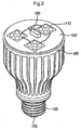
- FIG. 1 is an exploded perspective view illustrating a lighting apparatus according to the embodiment
- FIG. 2 is a perspective view illustrating a coupling structure of the lighting apparatus according to the embodiment
- FIG. 3 is an exploded perspective view illustrating a communication module shown in FIG. 1
- FIG. 4 is a sectional view taken along line A-A' of FIG. 1 .
- the lighting apparatus 100 includes a light source 110, a light source coupling part 120, a light distribution cover 130, a control module 140, a housing 150, a shield cover 160, a feeding cover 170, a heat sink 180, and a communication module 190.
- the light source 110 generates light.
- the light source 110 may include an LED.
- the light source 110 includes a feeding device 111, a plurality of feeding wires 113, a plurality of base substrates 115, and a plurality of LEDs 117.
- the feeding device 111 supplies power to the light source 110.
- the feeding device 111 may include a printed circuit board (PCB).
- the feeding wires 113 connect the feeding device 111 to the base substrates 115.
- the feeding wires 113 may directly connect the feeding device 111 to the base substrates 115, respectively.
- the feeding wires 113 may connect the feeding device 111 to some of the base substrates 115, and may connect the base substrates 115 to each other. Further, the feeding wires 113 transfer the power from the feeding device 111 to the base substrates 115.
- the base substrates 115 control driving of the light source 110.
- the base substrates 115 apply the power from the feeding device 111 to the LEDs.
- the base substrates 115 may include a PCB.
- the LEDs 117 are mounted on the base substrates 115. In this case, the LEDs 117 may be mounted on each of the base substrates 115. Further, the LEDs 117 emit the light according to the power from the base substrates 115. That is, the LEDs 117 output the light.
- the light source coupling unit 120 is coupled with the light source 110 to fix the light source 110.
- at least one first coupling hole 121 and at least one second coupling hole 123 are formed in the light source coupling unit 120.
- the first coupling holes 121 receive the base substrates 115, respectively.
- the light source coupling part 120 fixes the base substrates 115 and the LEDs 117 at positions of the first coupling holes 121, respectively. Further, the light coupling part 120 exposes the LEDs 117 through the first coupling holes 121, respectively.
- the second coupling hole 123 receives the feeding device 111 and the communication module 190. Moreover, the light source coupling part 120 exposes the feeding device 111 and the communication module 190 through the second coupling hole 123.
- the communication module 190 extends through the second coupling hole 123. That is, the communication module 190 protrudes in both directions about the light source coupling part 120 through the second coupling hole 123.
- the light source coupling part 120 may include an insulator.
- the light distribution cover 130 surrounds the light source 110 from the top of the light source coupling part 120.
- the light distribution cover 130 may have an open bulb shape. Further, the light distribution cover 130 protects the light source 110, and discharges the light emitted from the light source 110. In this case, the light distribution cover 130 distributes the light to a front surface or a rear surface of the lighting apparatus.
- the light distribution cover 130 may include at least one of glass, plastic, polypropylene (PP), and polyethylene (PE).
- the light distribution cover 130 may include polycarbonate (PC) having good lightfast, heat resistant and impact characteristics.
- the light distribution cover 130 may include an inner surface on which pigment is coated facing the light source 110. The pigment may include a diffusing agent to diffuse the light.
- the control module 140 controls an overall operation of the lighting apparatus 100.
- the control module 140 may include a main substrate and a plurality of components.
- the main substrate may include a PCB.
- the components are mounted on the main substrate and are electrically connected to the main substrate.
- the components include a converter and a driver.
- the converter is connected to an external power source through the main substrate. Further, the converter converts AC power of the external power source into DC power.
- the driver controls driving of the light source 110.
- control module 140 supplies power to the light source 110.
- the control module may include a power supply unit (PSU).
- PSU power supply unit
- the control module 140 may control the light source 110 according to a received wireless control signal.
- the control module 140 includes a feeding terminal 141 and a coupling terminal 143.
- the feeding terminal 141 is connected to the light source 110.
- the feeding terminal 141 makes contact with the feeding device 111 of the light source 110.
- the feeding terminal 141 protrudes from the control module 140.
- the feeding terminal 141 is coupled with the main substrate, and protrudes from the main substrate. Further, the feeding terminal 141 faces the feeding device 111.
- the feeding terminal 141 supplies power to the light source 110. That is, the control module 140 supplies the power to the light source 110 through the feeding device 111. Further, the feeding terminal 141 transmits a light source control signal for controlling the light source 110 to the light source 110. That is, the control module 140 transfers the light source control signal to the light source 110 through the feeding device 111.
- the coupling terminal 143 is connected to the communication module 190.
- the coupling terminal 143 is coupled with the communication module 190.
- the coupling terminal 143 may protrude from the control module 140.
- the coupling terminal 143 is coupled with the main substrate and protrudes from the main substrate. Further, the coupling terminal 143 may receive the communication module 190.
- a coupling groove 145 may be formed in the coupling terminal 143.
- the coupling groove 145 may face the communication module 190.
- the coupling groove 145 may receive the communication module 190.
- the coupling terminal 143 supplies the power to the communication module 190. That is, the control module 140 supplies the power to the communication module 190 through the coupling terminal 143. Further, the coupling terminal 143 receives a wireless control signal for controlling the control module 140 from the communication module 190. That is, the control module 140 receives the wireless control signal from the communication module 190 through the coupling terminal 143.
- the housing 150 receives the control module 140.
- a receiving hole 151 is formed in the housing 150. That is, the housing 150 receives the control module 140 through the receiving hole 151.
- the housing 150 may have a cylindrical shape. Further, the housing 150 may prevent an electrical short between the control module 140 and the heat sink 180.
- the housing 150 may include a material having superior insulation and durability. Further, the housing 150 may include a resin material.
- the housing 150 includes a connection terminal 153.
- the housing 150 is locked with the external power source through the connection terminal 153.
- the connection terminal 153 may be locked with the external power source through a socket scheme.
- the connection terminal 153 may be connected to the external power source. That is, the connection terminal 153 may be electrically connected to the external power source. Further, the connection terminal 153 may electrically connect the control module 140 to the external power source.
- the connection terminal 153 may include a conductive material.
- the shield cover 160 seals the housing 150.
- the shield cover 160 covers the receiving hole 151 of the housing 150 from the top of the housing 150.
- the shield cover 160 may prevent an electrical short between the control module 140 and the heat sink 180.
- the shield cover 160 may include a material having superior insulation and durability. Further, the shield cover 160 may include a resin material.
- At least one through hole 161 is formed in the shield cover 160.
- the through hole 161 is aligned on the same axis with the second coupling hole 123. Further, the through hole 161 receives the feeding terminal 141 and the communication module 190. In this case, the feeding terminal 141 and the communication module 190 extend through the through hole 161.
- the shield cover 160 exposes the feeding terminal 141 and the coupling terminal 143 through the through hole 161. That is, the through hole 161 protrudes the feeding terminal 141 toward the feeding device 111. Further, the through hole 161 protrudes the communication module 190 toward the coupling terminal 143.
- the feeding cover 170 seals the housing 150.
- the feeding cover 170 covers a receiving hole of the housing 150 from the bottom of the housing 150. Further, the feeding cover 170 makes contact with the external power source. In this case, the feeding cover 170 electrically connects the control module 140 to the external power source.
- the feeding cover 170 may include a conductive material.
- the heat sink 180 receives the control module 140, the housing 150, and the shield cover 160.
- a receiving groove (not shown) is formed in the heat sink 180. That is, the heat sink 180 receives the control module 140, the housing 150, and the shield cover 160 through the receiving groove.
- the light source 110 is mounted on the heat sink 180.
- the heat sink 180 releases heat generated from the light source 110, and protects the control module 140 from the heat generated from the light source 110.
- the heat sink 180 includes a first heat sink 181 and a second heat sink 185.
- the first heat sink 181 is disposed above the shield cover 160.
- the first heat sink 181 is coupled with the light distribution cover 130.
- an outer peripheral portion of the first heat sink 181 is coupled with the light distribution cover 130.
- the light source 110 and the light source coupling part 120 are mounted above the first heat sink 181.
- the first heat sink 181 makes contact with the light source 110.
- the first heat sink 181 moves the heat generated from the light source 110 to the second heat sink 185.
- the first heat sink 181 may have a circular shape or a plane shape.
- At least one insertion hole 183 is formed in the first heat sink 181.
- the insertion hole 183 is aligned on the same axis with the second coupling hole 123 and the through hole 161. Further, the insertion hole 183 receives the feeding terminal 141 and the communication module 190. In this case, the feeding terminal 141 and the communication module 190 extend through the insertion hole 183.
- the first heat sink 181 exposes the feeding terminal 141 and the coupling terminal 143 through the insertion hole 183. That is, the insertion hole 183 protrudes the feeding terminal 141 toward the feeding device 111. Further, the insertion hole 183 protrudes the communication module 190 toward the coupling terminal 143.
- the second heat sink 185 surrounds the housing 150.
- the second heat sink 185 exposes the connection terminal 153. That is, the second heat sink 185 surrounds the housing 150 except for a region of the connection terminal 153.
- the second heat sink 185 may have a cylindrical shape.
- the second heat sink 185 extends downward from the first heat sink 181. In this case, the second heat sink 185 releases the heat generated from the light source 110.
- a diameter of the second heat sink 185 may be gradually reduced downward along a central axis of the first heat sink 181.
- the second heat sink 185 includes a plurality of heat sink fins.
- the second heat sink 185 includes the heat sink fins 186 so that a surface area is increased.
- the heat sink fins 187 extend downward from the first heat sink 181.
- the heat sink fins 187 may be radially aligned about the central axis of the first heat sink 181.
- the heat sink fins 187 may protrude perpendicular to the central axis of the first heat sink 181.
- the communication module 190 receives a wireless control signal for controlling the lighting apparatus 100.
- the communication module 190 is connected to the control module 140.
- the communication module 190 is spaced apart from the light source 110 across the light source coupling part 120, the heat sink 180, and the shield cover 160.
- the communication module 190 is coupled with the control module 140.
- the communication module 190 includes a substrate 210, a connection terminal 220, a ground part 230, an antenna device 240, and a protective cover 250.
- the substrate 210 is provided in the communication module 190 for the purpose of support.
- the substrate 210 has a flat plate structure.
- the substrate 210 may include a PCB. Further, the substrate 210 may include a dielectric substance.
- the substrate 210 includes a connection region 211, a driving region 213, and an antenna region 215.
- connection region 211 is placed at one end of the substrate 210.
- the connection region 211 is opposed to the control module 140.
- the connection region 211 is opposed to the coupling terminal 143.
- the connection region 211 may be opposed to the coupling groove 145.
- the connection region 211 is inserted into the heat sink 180. In this case, the connection region is received in a receiving groove of the heat sink 180.
- the connection region 211 is coupled with the control module 140. In this case, the connection region 211 is locked with the coupling terminal 143.
- the connection region 211 may be inserted into the coupling groove 145.
- the driving region 213 extends from the connection region 211. In this case, the driving region 213 is placed at a center of the substrate 210. The driving region 213 extends across the light source coupling part 120, the heat sink 180, and the shield cover 160. The driving region 213 is inserted into the heat sink 180. In this case, the driving region 213 is received in the second coupling hole 123, the insertion hole 183, the through hole 161, and a receiving groove of the heat sink 180 which are aligned on the same axis.
- the driving region 213 includes a driving device (not shown).
- the driving device is embedded in the substrate 210, and is disposed in the driving region 213.
- the driving device extends from the driving region 213.
- one end of the driving device extends to the connection region 211, and another end of the driving device extends to the antenna region 215.
- the antenna region 215 is placed at the other end of the substrate 210.
- the antenna region 215 is placed in opposition to the connection region 211 about the driving region 213. Further, the antenna region 215 is connected to the connection region 211 through the driving region 213.
- the antenna region 215 protrudes from the heat sink 180.
- the antenna region 215 is exposed from the heat sink 180. In this case, the antenna region 215 is placed above the light coupling part 120.
- the antenna region 215 may be spaced apart from the light source 110.
- the connection terminal 220 serves as an interface for the control module 140 in the communication module 190.
- the connection terminal 200 is disposed at the connection region 211 of the substrate 210. In this case, the connection terminal 220 is connected to one end of the driving device. Further, the connection terminal 220 is connected to the control module 140. In this case, the connection terminal 220 is coupled with the coupling terminal 143 together with the connection region 211 and is connected to the coupling terminal 143.
- the connection terminal 220 may be inserted into a coupling groove 145. Power is supplied to the communication module 190 through the connection terminal 220. That is, the power is supplied from the coupling terminal 143 to the connection terminal 220.
- the ground part 230 is provided in the communication module 190 for the purpose of grounding.
- the ground part 230 is disposed at the connection region 211 of the substrate 210.
- the ground part 230 may be spaced apart from the connection terminal 220. That is, the ground part 230 may not make contact with the connection terminal 220.
- the ground part 230 may be connected to one end of the driving device.
- the antenna device 240 of the communication module 190 performs a wireless communication function.
- the antenna device 240 resonates at a preset frequency band to transmit/receive an electromagnetic wave.
- the antenna device 240 resonates at preset impedance.
- the antenna device 240 is disposed at the antenna region 215 of the substrate 210.
- the antenna device 240 is connected to another end of the driving device. That is, the antenna device 240 is connected to the connection terminal 220 through the driving device.
- the antenna device 240 may be connected to the ground part 230 through the driving device. One end of the antenna device 240 is connected to the driving device and another end of the antenna device 240 is open.
- the antenna device 240 protrudes from the heat sink 180.
- the antenna device 240 is disposed outside the heat sink 180. That is, the antenna device 240 is exposed from the heat sink 180 together with the antenna region 215. Further, the antenna device 240 is spaced apart from the heat sink 180. A spacing distance d between the antenna device 240 and the heat sink 180 may be approximately 1 mm or more. In this case, the antenna device 240 is placed above the light source coupling part 120. The antenna device 240 may be spaced apart from the light source 110.
- the antenna device 240 is driven using power supplied from the connection terminal 220. In this case, the antenna device 240 receives a wireless control signal for controlling the control module 140. In addition, the antenna device 240 transmits the wireless control signal to the control module 140. In this case, the antenna device 240 transmits the wireless control signal to the control module 140 through the connection terminal 220.
- an antenna device 240 may be formed in a patch type and then be attached to the antenna region 215.
- the antenna device 240 may be drawn with a conductive ink so as to be disposed at the antenna region 215.
- the antenna device 240 may be patterned at the antenna region 215.
- the antenna device 240 may include at least one of a bar type antenna element, a meander type antenna element, a spiral type antenna element, a step type antenna element, and a loop type antenna element.
- the antenna device 240 may include a conductive material.
- the antenna device 240 may include at least one of silver (Ag), palladium (Pd), platinum (Pt), copper (Cu), gold (Au), and nickel (Ni).
- the protective cover 250 receives the substrate 210. In this case, the protective cover 250 covers the substrate 210.
- the protective cover 250 covers the driving region 213 and the antenna region 215, and exposes the connection region 211.
- the protective cover 250 receives the antenna device 240, and exposes the connection terminal 220. That is, the connection terminal 220 protrudes from the protective cover 250.
- the protective cover 250 may include at least one of plastic, polypropylene (PP), polyethylene (PE), and polycarbonate (PC).
- the protective cover 250 includes a first protective cover 251 and a second protective cover 253.
- the first protective cover 251 surrounds the driving region 213.
- the first protective cover 251, together with the driving region 213, extends across the light source coupling part 120, the heat sink 180, and the shield cover 160.
- the protective cover 251 is inserted into the heat sink 180.
- the first protective cover 251 is received in the second coupling hole 123, the insertion hole 183, the through hole 161, and a receiving groove of the heat sink 180 which are aligned on the same axis.
- the second protective cover 253 receives the antenna region 215. Further, the second protective cover 253 receives the antenna device 240.
- the second protective cover 253 extends from the first protective cover 251. In this case, an insertion groove is formed in the second protective cover 253. That is, the second protective cover 253 receives the antenna device 240 together with the antenna region 215 through the insertion groove.
- the second protective cover 253 protrudes from the heat sink 180.
- the second protective cover 253 is exposed from the heat sink 180.
- the antenna device 240 is spaced apart from the heat sink 180 by the second protective cover 253.
- the second protective cover 253 is placed above the light source coupling part 120.
- the second protective cover 253 is locked with the heat sink 180.
- the second protective cover 253 has a size larger than a size of the insertion hole 183 so that the second protective cover 153 is not inserted into the heat sink 180.
- the lighting apparatus 100 has a wireless communication function.
- the lighting apparatus 100 may receive a wireless control signal through the communication module 190. Further, the lighting apparatus 100 may control the light source 110 according to the wireless control signal. Accordingly, the lighting apparatus 100 can be controlled in a wireless scheme. That is, a user of the lighting apparatus 100 may easily control the lighting apparatus 100. Accordingly, the convenience for a user of the lighting apparatus 100 can be improved.
Description
- The embodiment relates to a lighting apparatus.
- In general, various types of lighting apparatuses such as ceiling-mounting type lamps, scenery lighting lamps, sleeping lamps, and stand lamps exist according to purposes thereof. The lighting apparatuses must irradiate light with sufficient luminance level according to purposes. Accordingly, recently, a light emitting diode (LED) has been used for a lighting apparatus. In comparison with other light sources such as a fluorescent lamp and an incandescent lamp, the LED is advantageous because of low power consumption, a long lifetime, a fast response time, safety, and environment-friendliness. Accordingly, many studies and researches to replace the existing light sources with the light emitting diode have been carried out.
WO 2010/140136 A1 discloses a lighting apparatus. - However, the above lighting apparatuses are turned-on/off by a switch connected to the lighting apparatuses through a cable. Accordingly, a user of the lighting apparatus must inconveniently control the lighting apparatus.
- An invention provides a lighting apparatus which can be easily controlled.
- According to the invention, there is provided a lighting apparatus according to claim 1.
- The lighting apparatus according to the embodiment has a wireless communication function. In this case, the lighting apparatus may receive a wireless control signal through the communication module. Further, the lighting apparatus may control the light source according to the wireless control signal. Accordingly, the lighting apparatus can be controlled in a wireless scheme. That is, a user of the lighting apparatus can easily control the lighting apparatus. Accordingly, the convenience for a user of the lighting apparatus can be improved.
-
-
FIG. 1 is an exploded perspective view illustrating a lighting apparatus according to the invention. -
FIG. 2 is a perspective view illustrating a coupling structure of the lighting apparatus according to the invention. -
FIG. 3 is an exploded perspective view illustrating a communication module shown inFIG. 1 . -
FIG. 4 is a sectional view taken along line A-A' ofFIG. 1 . - Hereinafter, the embodiments will be described in detail with reference to accompanying drawings. In the accompanying drawings, the same components will be assigned with the same reference numerals. In a description of the embodiment, if the function or the structure related to the disclosure and generally known to those skilled in the art make the subject matter of the disclosure unclear, the details of the function or the structure will be omitted.
- In the description of the embodiments, it will be understood that, when each element is referred to as being "on" or "under" another element, it can be "directly" or "indirectly" on or under another element or the other constituent elements may also be present. Such a position of the elements has been described with reference to the drawings.
-
FIG. 1 is an exploded perspective view illustrating a lighting apparatus according to the embodiment,FIG. 2 is a perspective view illustrating a coupling structure of the lighting apparatus according to the embodiment,FIG. 3 is an exploded perspective view illustrating a communication module shown inFIG. 1 , andFIG. 4 is a sectional view taken along line A-A' ofFIG. 1 . - Referring to
FIGS. 1 to 4 , thelighting apparatus 100 according to the embodiment includes alight source 110, a lightsource coupling part 120, alight distribution cover 130, acontrol module 140, ahousing 150, ashield cover 160, afeeding cover 170, aheat sink 180, and acommunication module 190. - The
light source 110 generates light. In this case, thelight source 110 may include an LED. Thelight source 110 includes afeeding device 111, a plurality offeeding wires 113, a plurality ofbase substrates 115, and a plurality ofLEDs 117. - The
feeding device 111 supplies power to thelight source 110. Thefeeding device 111 may include a printed circuit board (PCB). - The
feeding wires 113 connect thefeeding device 111 to thebase substrates 115. In this case, thefeeding wires 113 may directly connect thefeeding device 111 to thebase substrates 115, respectively. Thefeeding wires 113 may connect thefeeding device 111 to some of thebase substrates 115, and may connect thebase substrates 115 to each other. Further, thefeeding wires 113 transfer the power from thefeeding device 111 to thebase substrates 115. - The
base substrates 115 control driving of thelight source 110. In this case, thebase substrates 115 apply the power from thefeeding device 111 to the LEDs. Thebase substrates 115 may include a PCB. - The
LEDs 117 are mounted on thebase substrates 115. In this case, theLEDs 117 may be mounted on each of thebase substrates 115. Further, theLEDs 117 emit the light according to the power from thebase substrates 115. That is, theLEDs 117 output the light. - The light
source coupling unit 120 is coupled with thelight source 110 to fix thelight source 110. In this case, at least onefirst coupling hole 121 and at least onesecond coupling hole 123 are formed in the lightsource coupling unit 120. Thefirst coupling holes 121 receive thebase substrates 115, respectively. The lightsource coupling part 120 fixes thebase substrates 115 and theLEDs 117 at positions of thefirst coupling holes 121, respectively. Further, thelight coupling part 120 exposes theLEDs 117 through thefirst coupling holes 121, respectively. In addition, thesecond coupling hole 123 receives thefeeding device 111 and thecommunication module 190. Moreover, the lightsource coupling part 120 exposes thefeeding device 111 and thecommunication module 190 through thesecond coupling hole 123. Thecommunication module 190 extends through thesecond coupling hole 123. That is, thecommunication module 190 protrudes in both directions about the lightsource coupling part 120 through thesecond coupling hole 123. The lightsource coupling part 120 may include an insulator. - The
light distribution cover 130 surrounds thelight source 110 from the top of the lightsource coupling part 120. Thelight distribution cover 130 may have an open bulb shape. Further, thelight distribution cover 130 protects thelight source 110, and discharges the light emitted from thelight source 110. In this case, thelight distribution cover 130 distributes the light to a front surface or a rear surface of the lighting apparatus. Thelight distribution cover 130 may include at least one of glass, plastic, polypropylene (PP), and polyethylene (PE). Thelight distribution cover 130 may include polycarbonate (PC) having good lightfast, heat resistant and impact characteristics. Thelight distribution cover 130 may include an inner surface on which pigment is coated facing thelight source 110. The pigment may include a diffusing agent to diffuse the light. - The
control module 140 controls an overall operation of thelighting apparatus 100. In this case, although not shown, thecontrol module 140 may include a main substrate and a plurality of components. The main substrate may include a PCB. The components are mounted on the main substrate and are electrically connected to the main substrate. The components include a converter and a driver. The converter is connected to an external power source through the main substrate. Further, the converter converts AC power of the external power source into DC power. The driver controls driving of thelight source 110. - In addition, the
control module 140 supplies power to thelight source 110. The control module may include a power supply unit (PSU). In this case, thecontrol module 140 may control thelight source 110 according to a received wireless control signal. Thecontrol module 140 includes a feedingterminal 141 and acoupling terminal 143. - The feeding
terminal 141 is connected to thelight source 110. The feedingterminal 141 makes contact with thefeeding device 111 of thelight source 110. In this case, the feedingterminal 141 protrudes from thecontrol module 140. The feedingterminal 141 is coupled with the main substrate, and protrudes from the main substrate. Further, the feedingterminal 141 faces thefeeding device 111. - In addition, the feeding
terminal 141 supplies power to thelight source 110. That is, thecontrol module 140 supplies the power to thelight source 110 through thefeeding device 111. Further, the feedingterminal 141 transmits a light source control signal for controlling thelight source 110 to thelight source 110. That is, thecontrol module 140 transfers the light source control signal to thelight source 110 through thefeeding device 111. - The
coupling terminal 143 is connected to thecommunication module 190. Thecoupling terminal 143 is coupled with thecommunication module 190. In this case, thecoupling terminal 143 may protrude from thecontrol module 140. Thecoupling terminal 143 is coupled with the main substrate and protrudes from the main substrate. Further, thecoupling terminal 143 may receive thecommunication module 190. Acoupling groove 145 may be formed in thecoupling terminal 143. Thecoupling groove 145 may face thecommunication module 190. Moreover, thecoupling groove 145 may receive thecommunication module 190. - In addition, the
coupling terminal 143 supplies the power to thecommunication module 190. That is, thecontrol module 140 supplies the power to thecommunication module 190 through thecoupling terminal 143. Further, thecoupling terminal 143 receives a wireless control signal for controlling thecontrol module 140 from thecommunication module 190. That is, thecontrol module 140 receives the wireless control signal from thecommunication module 190 through thecoupling terminal 143. - The
housing 150 receives thecontrol module 140. A receivinghole 151 is formed in thehousing 150. That is, thehousing 150 receives thecontrol module 140 through the receivinghole 151. In this case, thehousing 150 may have a cylindrical shape. Further, thehousing 150 may prevent an electrical short between thecontrol module 140 and theheat sink 180. Thehousing 150 may include a material having superior insulation and durability. Further, thehousing 150 may include a resin material. - In addition, the
housing 150 includes aconnection terminal 153. In this case, thehousing 150 is locked with the external power source through theconnection terminal 153. Theconnection terminal 153 may be locked with the external power source through a socket scheme. Further, theconnection terminal 153 may be connected to the external power source. That is, theconnection terminal 153 may be electrically connected to the external power source. Further, theconnection terminal 153 may electrically connect thecontrol module 140 to the external power source. Theconnection terminal 153 may include a conductive material. - The shield cover 160 seals the
housing 150. Theshield cover 160 covers the receivinghole 151 of thehousing 150 from the top of thehousing 150. In this case, theshield cover 160 may prevent an electrical short between thecontrol module 140 and theheat sink 180. Theshield cover 160 may include a material having superior insulation and durability. Further, theshield cover 160 may include a resin material. - At least one through
hole 161 is formed in theshield cover 160. The throughhole 161 is aligned on the same axis with thesecond coupling hole 123. Further, the throughhole 161 receives the feedingterminal 141 and thecommunication module 190. In this case, the feedingterminal 141 and thecommunication module 190 extend through the throughhole 161. Theshield cover 160 exposes the feedingterminal 141 and thecoupling terminal 143 through the throughhole 161. That is, the throughhole 161 protrudes the feedingterminal 141 toward thefeeding device 111. Further, the throughhole 161 protrudes thecommunication module 190 toward thecoupling terminal 143. - The feeding
cover 170 seals thehousing 150. The feedingcover 170 covers a receiving hole of thehousing 150 from the bottom of thehousing 150. Further, the feedingcover 170 makes contact with the external power source. In this case, the feedingcover 170 electrically connects thecontrol module 140 to the external power source. The feedingcover 170 may include a conductive material. - The
heat sink 180 receives thecontrol module 140, thehousing 150, and theshield cover 160. A receiving groove (not shown) is formed in theheat sink 180. That is, theheat sink 180 receives thecontrol module 140, thehousing 150, and theshield cover 160 through the receiving groove. Further, thelight source 110 is mounted on theheat sink 180. In addition, theheat sink 180 releases heat generated from thelight source 110, and protects thecontrol module 140 from the heat generated from thelight source 110. In this case, theheat sink 180 includes afirst heat sink 181 and asecond heat sink 185. - The
first heat sink 181 is disposed above theshield cover 160. Thefirst heat sink 181 is coupled with thelight distribution cover 130. In this case, an outer peripheral portion of thefirst heat sink 181 is coupled with thelight distribution cover 130. Further, thelight source 110 and the lightsource coupling part 120 are mounted above thefirst heat sink 181. Thefirst heat sink 181 makes contact with thelight source 110. In this case, thefirst heat sink 181 moves the heat generated from thelight source 110 to thesecond heat sink 185. Thefirst heat sink 181 may have a circular shape or a plane shape. - At least one
insertion hole 183 is formed in thefirst heat sink 181. Theinsertion hole 183 is aligned on the same axis with thesecond coupling hole 123 and the throughhole 161. Further, theinsertion hole 183 receives the feedingterminal 141 and thecommunication module 190. In this case, the feedingterminal 141 and thecommunication module 190 extend through theinsertion hole 183. Thefirst heat sink 181 exposes the feedingterminal 141 and thecoupling terminal 143 through theinsertion hole 183. That is, theinsertion hole 183 protrudes the feedingterminal 141 toward thefeeding device 111. Further, theinsertion hole 183 protrudes thecommunication module 190 toward thecoupling terminal 143. - The
second heat sink 185 surrounds thehousing 150. In this case, thesecond heat sink 185 exposes theconnection terminal 153. That is, thesecond heat sink 185 surrounds thehousing 150 except for a region of theconnection terminal 153. Thesecond heat sink 185 may have a cylindrical shape. Thesecond heat sink 185 extends downward from thefirst heat sink 181. In this case, thesecond heat sink 185 releases the heat generated from thelight source 110. A diameter of thesecond heat sink 185 may be gradually reduced downward along a central axis of thefirst heat sink 181. - Further, the
second heat sink 185 includes a plurality of heat sink fins. In this case, thesecond heat sink 185 includes the heat sink fins 186 so that a surface area is increased. Theheat sink fins 187 extend downward from thefirst heat sink 181. In this case, theheat sink fins 187 may be radially aligned about the central axis of thefirst heat sink 181. Theheat sink fins 187 may protrude perpendicular to the central axis of thefirst heat sink 181. - The
communication module 190 receives a wireless control signal for controlling thelighting apparatus 100. In this case, thecommunication module 190 is connected to thecontrol module 140. Thecommunication module 190 is spaced apart from thelight source 110 across the lightsource coupling part 120, theheat sink 180, and theshield cover 160. In addition, thecommunication module 190 is coupled with thecontrol module 140. Thecommunication module 190 includes asubstrate 210, aconnection terminal 220, aground part 230, anantenna device 240, and aprotective cover 250. - The
substrate 210 is provided in thecommunication module 190 for the purpose of support. In this case, thesubstrate 210 has a flat plate structure. Thesubstrate 210 may include a PCB. Further, thesubstrate 210 may include a dielectric substance. Thesubstrate 210 includes aconnection region 211, a drivingregion 213, and anantenna region 215. - The
connection region 211 is placed at one end of thesubstrate 210. Theconnection region 211 is opposed to thecontrol module 140. In this case, theconnection region 211 is opposed to thecoupling terminal 143. Theconnection region 211 may be opposed to thecoupling groove 145. In addition, theconnection region 211 is inserted into theheat sink 180. In this case, the connection region is received in a receiving groove of theheat sink 180. Further, theconnection region 211 is coupled with thecontrol module 140. In this case, theconnection region 211 is locked with thecoupling terminal 143. Theconnection region 211 may be inserted into thecoupling groove 145. - The driving
region 213 extends from theconnection region 211. In this case, the drivingregion 213 is placed at a center of thesubstrate 210. The drivingregion 213 extends across the lightsource coupling part 120, theheat sink 180, and theshield cover 160. The drivingregion 213 is inserted into theheat sink 180. In this case, the drivingregion 213 is received in thesecond coupling hole 123, theinsertion hole 183, the throughhole 161, and a receiving groove of theheat sink 180 which are aligned on the same axis. - Further, the driving
region 213 includes a driving device (not shown). In this case, the driving device is embedded in thesubstrate 210, and is disposed in the drivingregion 213. The driving device extends from the drivingregion 213. In addition, one end of the driving device extends to theconnection region 211, and another end of the driving device extends to theantenna region 215. - The
antenna region 215 is placed at the other end of thesubstrate 210. Theantenna region 215 is placed in opposition to theconnection region 211 about the drivingregion 213. Further, theantenna region 215 is connected to theconnection region 211 through the drivingregion 213. Theantenna region 215 protrudes from theheat sink 180. Theantenna region 215 is exposed from theheat sink 180. In this case, theantenna region 215 is placed above thelight coupling part 120. Theantenna region 215 may be spaced apart from thelight source 110. - The
connection terminal 220 serves as an interface for thecontrol module 140 in thecommunication module 190. The connection terminal 200 is disposed at theconnection region 211 of thesubstrate 210. In this case, theconnection terminal 220 is connected to one end of the driving device. Further, theconnection terminal 220 is connected to thecontrol module 140. In this case, theconnection terminal 220 is coupled with thecoupling terminal 143 together with theconnection region 211 and is connected to thecoupling terminal 143. Theconnection terminal 220 may be inserted into acoupling groove 145. Power is supplied to thecommunication module 190 through theconnection terminal 220. That is, the power is supplied from thecoupling terminal 143 to theconnection terminal 220. - The
ground part 230 is provided in thecommunication module 190 for the purpose of grounding. Theground part 230 is disposed at theconnection region 211 of thesubstrate 210. In this case, theground part 230 may be spaced apart from theconnection terminal 220. That is, theground part 230 may not make contact with theconnection terminal 220. Moreover, theground part 230 may be connected to one end of the driving device. - The
antenna device 240 of thecommunication module 190 performs a wireless communication function. In this case, theantenna device 240 resonates at a preset frequency band to transmit/receive an electromagnetic wave. Theantenna device 240 resonates at preset impedance. In this case, theantenna device 240 is disposed at theantenna region 215 of thesubstrate 210. In this case, theantenna device 240 is connected to another end of the driving device. That is, theantenna device 240 is connected to theconnection terminal 220 through the driving device. Theantenna device 240 may be connected to theground part 230 through the driving device. One end of theantenna device 240 is connected to the driving device and another end of theantenna device 240 is open. - In addition, the
antenna device 240 protrudes from theheat sink 180. Theantenna device 240 is disposed outside theheat sink 180. That is, theantenna device 240 is exposed from theheat sink 180 together with theantenna region 215. Further, theantenna device 240 is spaced apart from theheat sink 180. A spacing distance d between theantenna device 240 and theheat sink 180 may be approximately 1 mm or more. In this case, theantenna device 240 is placed above the lightsource coupling part 120. Theantenna device 240 may be spaced apart from thelight source 110. - Further, the
antenna device 240 is driven using power supplied from theconnection terminal 220. In this case, theantenna device 240 receives a wireless control signal for controlling thecontrol module 140. In addition, theantenna device 240 transmits the wireless control signal to thecontrol module 140. In this case, theantenna device 240 transmits the wireless control signal to thecontrol module 140 through theconnection terminal 220. - In this case, an
antenna device 240 may be formed in a patch type and then be attached to theantenna region 215. Theantenna device 240 may be drawn with a conductive ink so as to be disposed at theantenna region 215. Theantenna device 240 may be patterned at theantenna region 215. Theantenna device 240 may include at least one of a bar type antenna element, a meander type antenna element, a spiral type antenna element, a step type antenna element, and a loop type antenna element. In this case, theantenna device 240 may include a conductive material. Theantenna device 240 may include at least one of silver (Ag), palladium (Pd), platinum (Pt), copper (Cu), gold (Au), and nickel (Ni). - The
protective cover 250 receives thesubstrate 210. In this case, theprotective cover 250 covers thesubstrate 210. Theprotective cover 250 covers the drivingregion 213 and theantenna region 215, and exposes theconnection region 211. Theprotective cover 250 receives theantenna device 240, and exposes theconnection terminal 220. That is, theconnection terminal 220 protrudes from theprotective cover 250. Theprotective cover 250 may include at least one of plastic, polypropylene (PP), polyethylene (PE), and polycarbonate (PC). Theprotective cover 250 includes a firstprotective cover 251 and a secondprotective cover 253. - The first
protective cover 251 surrounds the drivingregion 213. The firstprotective cover 251, together with the drivingregion 213, extends across the lightsource coupling part 120, theheat sink 180, and theshield cover 160. Theprotective cover 251 is inserted into theheat sink 180. In this case, the firstprotective cover 251 is received in thesecond coupling hole 123, theinsertion hole 183, the throughhole 161, and a receiving groove of theheat sink 180 which are aligned on the same axis. - The second
protective cover 253 receives theantenna region 215. Further, the secondprotective cover 253 receives theantenna device 240. The secondprotective cover 253 extends from the firstprotective cover 251. In this case, an insertion groove is formed in the secondprotective cover 253. That is, the secondprotective cover 253 receives theantenna device 240 together with theantenna region 215 through the insertion groove. - In addition, the second
protective cover 253 protrudes from theheat sink 180. The secondprotective cover 253 is exposed from theheat sink 180. In this case, theantenna device 240 is spaced apart from theheat sink 180 by the secondprotective cover 253. The secondprotective cover 253 is placed above the lightsource coupling part 120. In addition, the secondprotective cover 253 is locked with theheat sink 180. In this case, the secondprotective cover 253 has a size larger than a size of theinsertion hole 183 so that the secondprotective cover 153 is not inserted into theheat sink 180. - According to the embodiment, the
lighting apparatus 100 has a wireless communication function. In this case, thelighting apparatus 100 may receive a wireless control signal through thecommunication module 190. Further, thelighting apparatus 100 may control thelight source 110 according to the wireless control signal. Accordingly, thelighting apparatus 100 can be controlled in a wireless scheme. That is, a user of thelighting apparatus 100 may easily control thelighting apparatus 100. Accordingly, the convenience for a user of thelighting apparatus 100 can be improved.
Claims (11)
- A lighting apparatus (100) comprising:a control module (140) supplying power;a heat sink (180) receiving the control module (140);a light source (110) mounted on the heat sink (180) and connected to the control module (140); anda communication module (190) comprising a substrate (210) on which an antenna device (240) is disposed,characterized in thata connection terminal (220) is provided on the substrate (210), wherein an insertion hole (183) is formed in the heat sink (180) and the substrate (210) extends by passing through the insertion hole (183) in such a way, that the connection terminal (220) is inserted into the heat sink (180) and the antenna device (240) is protruding from the heat sink (180),wherein the control module (140) comprises a coupling terminal (143) to receive the connection terminal (220) for connecting the communication module (190) to the control module (140).
- The lighting apparatus (100) of claim 1, wherein the antenna device (240) is spaced apart from the heat sink (180).
- The lighting apparatus (100) of claim 1, wherein the substrate (210) comprises:a connection region (211) on which the connection terminal (220) is disposed;and an antenna region (215) on which the antenna device (240) is disposed.
- The lighting apparatus (100) of any one of claims 1 to 3, wherein the communication module (190) further comprises a driving device connecting the connection terminal (220) to the antenna device (240) and driving the antenna device (240).
- The lighting apparatus (100) of any one of claims 1 to 5, wherein the communication module (190) further comprises a protective cover (250) covering the substrate (210) to receive the antenna device (240), and exposing the connection terminal (220).
- The lighting apparatus (100) of claim 4 or 5, wherein the substrate (210) further comprises a ground part (230) spaced apart from the connection terminal (220) while making contact with the antenna device (240) through the driving device.
- The lighting apparatus (100) of claim 6, wherein the ground part (230) is disposed at the connection region (211).
- The lighting apparatus (100) of any one of claims 4 to 7, wherein the substrate (210) further comprises a driving region (213) interposed between the connection region (211) and the antenna region and on which the driving device is disposed.
- The lighting apparatus (100) of any one of claims 5 to 8, wherein the protective cover (250) comprises:a first protective cover (251) inserted into the heat sink (180); anda second protective cover (253) coupled with the heat sink (180) and protruding from the heat sink (180).
- The lighting apparatus (100) of any one of claims 2 to 9, wherein a spacing distance between the heat sink (180) and the antenna device (240) is 1 mm or more.
- The lighting apparatus (100) of any one of claims 1 to 10, wherein the control module (140) further comprises a feeding terminal (141) connected to the light source (110).
Priority Applications (1)
| Application Number | Priority Date | Filing Date | Title |
|---|---|---|---|
| EP15195117.5A EP3026336B8 (en) | 2012-07-23 | 2013-07-22 | Lighting apparatus |
Applications Claiming Priority (1)
| Application Number | Priority Date | Filing Date | Title |
|---|---|---|---|
| KR1020120079877A KR101360678B1 (en) | 2012-07-23 | 2012-07-23 | Lighting apparatus |
Related Child Applications (2)
| Application Number | Title | Priority Date | Filing Date |
|---|---|---|---|
| EP15195117.5A Division EP3026336B8 (en) | 2012-07-23 | 2013-07-22 | Lighting apparatus |
| EP15195117.5A Division-Into EP3026336B8 (en) | 2012-07-23 | 2013-07-22 | Lighting apparatus |
Publications (2)
| Publication Number | Publication Date |
|---|---|
| EP2690359A1 EP2690359A1 (en) | 2014-01-29 |
| EP2690359B1 true EP2690359B1 (en) | 2016-03-30 |
Family
ID=48875539
Family Applications (2)
| Application Number | Title | Priority Date | Filing Date |
|---|---|---|---|
| EP13177439.0A Active EP2690359B1 (en) | 2012-07-23 | 2013-07-22 | Lighting apparatus |
| EP15195117.5A Active EP3026336B8 (en) | 2012-07-23 | 2013-07-22 | Lighting apparatus |
Family Applications After (1)
| Application Number | Title | Priority Date | Filing Date |
|---|---|---|---|
| EP15195117.5A Active EP3026336B8 (en) | 2012-07-23 | 2013-07-22 | Lighting apparatus |
Country Status (4)
| Country | Link |
|---|---|
| US (3) | US9253859B2 (en) |
| EP (2) | EP2690359B1 (en) |
| JP (2) | JP5714664B2 (en) |
| KR (1) | KR101360678B1 (en) |
Families Citing this family (40)
| Publication number | Priority date | Publication date | Assignee | Title |
|---|---|---|---|---|
| US9488324B2 (en) * | 2011-09-02 | 2016-11-08 | Soraa, Inc. | Accessories for LED lamp systems |
| CN107613413B (en) | 2012-03-21 | 2021-05-04 | 鲍尔卡斯特公司 | Wireless sensor system, method and apparatus with switch and socket control |
| US11221110B2 (en) * | 2013-03-13 | 2022-01-11 | Smartbotics, Inc. | LED light bulb construction and manufacture |
| CN105122544B (en) * | 2013-04-23 | 2017-04-12 | 飞利浦照明控股有限公司 | A lighting device and luminaire comprising an antenna |
| US10047912B2 (en) | 2013-10-15 | 2018-08-14 | LIFI Labs, Inc. | Lighting assembly |
| WO2015061542A1 (en) * | 2013-10-23 | 2015-04-30 | Greene Charles E | Automated system for lighting control |
| US11455884B2 (en) | 2014-09-02 | 2022-09-27 | LIFI Labs, Inc. | Lighting system |
| US9210779B2 (en) | 2013-11-14 | 2015-12-08 | LIFI Labs, Inc. | Resettable lighting system and method |
| KR20150109656A (en) * | 2014-03-20 | 2015-10-02 | 엘지이노텍 주식회사 | Lighting apparatus |
| US9538623B2 (en) * | 2014-05-12 | 2017-01-03 | Lg Electronics Inc. | Lighting device |
| US9435521B2 (en) | 2014-05-21 | 2016-09-06 | Technical Consumer Products, Inc. | Antenna element for a directional lighting fixture |
| CN106465499B (en) | 2014-05-22 | 2018-11-30 | 莱弗实验室公司 | Directional illumination system and method |
| US9488352B2 (en) | 2014-05-28 | 2016-11-08 | Technical Consumer Products, Inc. | Radio frequency (RF) signal pathway for a lamp antenna |
| US9210773B1 (en) * | 2014-05-29 | 2015-12-08 | Technical Consumer Products, Inc. | Wireless light fixture |
| JP6473925B2 (en) * | 2014-09-11 | 2019-02-27 | パナソニックIpマネジメント株式会社 | lighting equipment |
| US9949348B2 (en) * | 2014-11-10 | 2018-04-17 | LIFI Labs, Inc. | Lighting connectivity module |
| JP6969592B2 (en) * | 2015-01-21 | 2021-11-24 | 三菱電機株式会社 | lighting equipment |
| WO2016146339A1 (en) * | 2015-03-17 | 2016-09-22 | Philips Lighting Holding B.V. | Lighting device with first and second coupled and inter-movable antennas |
| WO2016176372A1 (en) * | 2015-04-27 | 2016-11-03 | Osram Sylvania Inc. | Wireless mounted control module |
| JP6579511B2 (en) * | 2015-05-11 | 2019-09-25 | パナソニックIpマネジメント株式会社 | Light source unit and lighting fixture equipped with the same |
| US10317018B2 (en) * | 2015-09-01 | 2019-06-11 | Lg Innotek Co., Ltd. | Lighting device |
| EP3523881B1 (en) | 2016-10-07 | 2022-12-14 | Powercast Corporation | Automated system for lighting control |
| US10440794B2 (en) | 2016-11-02 | 2019-10-08 | LIFI Labs, Inc. | Lighting system and method |
| JP2018137113A (en) * | 2017-02-21 | 2018-08-30 | パナソニックIpマネジメント株式会社 | Lighting device and light fitting |
| BE1026104B1 (en) * | 2018-03-16 | 2019-10-14 | Schreder S.A. | CONNECTED LUMINAIRE |
| CN112204813A (en) * | 2018-05-31 | 2021-01-08 | 昕诺飞控股有限公司 | Stacked circuit boards in lighting devices |
| JP7291200B2 (en) | 2018-07-16 | 2023-06-14 | シグニファイ ホールディング ビー ヴィ | Lighting device and method |
| CN108944653A (en) * | 2018-09-14 | 2018-12-07 | 常州瑞阳电装有限公司 | A kind of universe formula flasher driving circuit |
| CN209130543U (en) * | 2018-11-13 | 2019-07-19 | 漳州立达信光电子科技有限公司 | A kind of intelligent lamp |
| CN109511207A (en) * | 2019-01-09 | 2019-03-22 | 苏州蓝石新动力有限公司 | A kind of light synchronous method and system |
| CA3135800A1 (en) | 2019-04-03 | 2020-10-08 | Lutron Technology Company Llc | Wireless controllable lighting device |
| JP6840188B2 (en) * | 2019-05-07 | 2021-03-10 | 三菱電機株式会社 | lighting equipment |
| CN211625172U (en) * | 2020-01-16 | 2020-10-02 | 漳州立达信光电子科技有限公司 | Light source intelligent component and radio frequency control lighting lamp with same |
| JP7330560B2 (en) * | 2020-06-23 | 2023-08-22 | アイリスオーヤマ株式会社 | Light-emitting unit and lighting device |
| US11774079B1 (en) | 2020-06-28 | 2023-10-03 | Hangzhou Tuya Information Technology Co., Ltd. | Light board structure and light fixture having the same |
| JP7291977B2 (en) * | 2020-08-29 | 2023-06-16 | アイリスオーヤマ株式会社 | lighting equipment |
| US20230408080A1 (en) * | 2020-11-06 | 2023-12-21 | Signify Holding B.V. | Luminaire with integrated rf communication |
| CA3203653A1 (en) | 2021-01-13 | 2022-07-21 | Matthew V. Harte | Controllable lighting device |
| CA3204554A1 (en) | 2021-01-13 | 2022-07-21 | Aaron J. WILZ | Wireless controllable lighting device |
| WO2024033242A1 (en) | 2022-08-12 | 2024-02-15 | Signify Holding B.V. | Luminaire driver with antenna module |
Family Cites Families (35)
| Publication number | Priority date | Publication date | Assignee | Title |
|---|---|---|---|---|
| US6295031B1 (en) * | 1993-12-23 | 2001-09-25 | Symbol Technologies, Inc. | Memory card assembly having an integral antenna |
| JPH10190511A (en) * | 1996-12-26 | 1998-07-21 | Nec Kansai Ltd | Antenna system for radio equipment |
| US7318659B2 (en) * | 2004-03-03 | 2008-01-15 | S. C. Johnson & Son, Inc. | Combination white light and colored LED light device with active ingredient emission |
| JP2005051728A (en) * | 2003-07-15 | 2005-02-24 | Toshiba Lighting & Technology Corp | Load control system |
| TWI329724B (en) | 2003-09-09 | 2010-09-01 | Koninkl Philips Electronics Nv | Integrated lamp with feedback and wireless control |
| GB0415606D0 (en) | 2004-07-10 | 2004-08-18 | Koninkl Philips Electronics Nv | Lighting fixtures incorporating rf antennae |
| KR20040080398A (en) | 2004-08-03 | 2004-09-18 | 권대웅 | Backward Sensor Lamp Interface Use Microwave Sensor Module And New Light Source |
| GB0520975D0 (en) * | 2005-10-14 | 2005-11-23 | Noble Barry A | Programmable lighting device |
| KR100884944B1 (en) | 2006-05-29 | 2009-02-23 | 주식회사 엘지화학 | Voltage Sensing Member and Battery Module Employed with the Same |
| US8203445B2 (en) | 2006-03-28 | 2012-06-19 | Wireless Environment, Llc | Wireless lighting |
| US8491159B2 (en) | 2006-03-28 | 2013-07-23 | Wireless Environment, Llc | Wireless emergency lighting system |
| JP2008028734A (en) * | 2006-07-21 | 2008-02-07 | Hitachi Metals Ltd | Surface mounting antenna and communication apparatus mounting it |
| US8791655B2 (en) * | 2009-05-09 | 2014-07-29 | Innosys, Inc. | LED lamp with remote control |
| WO2010140136A1 (en) * | 2009-06-05 | 2010-12-09 | Koninklijke Philips Electronics N.V. | Lighting device with built-in rf antenna |
| KR100945459B1 (en) | 2009-07-15 | 2010-03-05 | (주)연호전자 | A heat dissipating device of led lamp |
| US8414178B2 (en) | 2009-08-12 | 2013-04-09 | Journée Lighting, Inc. | LED light module for use in a lighting assembly |
| CN102086982A (en) | 2009-12-04 | 2011-06-08 | 阳泰电子股份有限公司 | Serially connectable light emitting diode bulb |
| CN201661913U (en) * | 2010-03-31 | 2010-12-01 | 苏州久腾光电科技有限公司 | Wireless intelligent control LED lamp |
| WO2011129309A1 (en) | 2010-04-12 | 2011-10-20 | シャープ株式会社 | Illumination device and illumination system |
| JP2011228130A (en) | 2010-04-20 | 2011-11-10 | Fujikom Corp | Led bulb |
| KR101009505B1 (en) | 2010-06-09 | 2011-01-18 | 이동수 | Led module maintainable heat dissipation without extra heat dissipating device |
| JP2012079498A (en) * | 2010-09-30 | 2012-04-19 | Toshiba Lighting & Technology Corp | Light-emitting device and lighting fixture |
| EP2450613B1 (en) * | 2010-11-08 | 2015-01-28 | LG Innotek Co., Ltd. | Lighting device |
| US8314571B2 (en) * | 2010-12-14 | 2012-11-20 | Greenwave Reality, Pte, Ltd. | Light with changeable color temperature |
| JP4944282B1 (en) * | 2011-01-25 | 2012-05-30 | パナソニック株式会社 | Light source for illumination |
| CN202056583U (en) | 2011-04-01 | 2011-11-30 | 东莞市欣光源电子有限公司 | Intelligent human body induction integral LED bulb lamp |
| JP5793662B2 (en) * | 2011-04-20 | 2015-10-14 | パナソニックIpマネジメント株式会社 | Light source for illumination |
| US9217555B2 (en) * | 2011-05-17 | 2015-12-22 | Bridgelux Incorporated | LED module with integrated thermal spreader |
| WO2013031043A1 (en) * | 2011-08-29 | 2013-03-07 | パナソニック株式会社 | Lamp and lighting apparatus |
| WO2013103698A1 (en) * | 2012-01-06 | 2013-07-11 | Thermal Solution Resources, Llc | Led lamps with enhanced wireless communication |
| JP5817532B2 (en) | 2012-01-06 | 2015-11-18 | ソニー株式会社 | Light bulb type light source device |
| KR101349513B1 (en) | 2012-03-20 | 2014-01-09 | 엘지이노텍 주식회사 | Lighting apparatus and lighting system |
| JP5880245B2 (en) * | 2012-04-18 | 2016-03-08 | ソニー株式会社 | Light bulb type light source device |
| US8633646B2 (en) * | 2012-04-30 | 2014-01-21 | Freescale Semiconductor, Inc. | Method and apparatus for radio-frequency controllable LED lamp fixture antenna |
| US10047912B2 (en) | 2013-10-15 | 2018-08-14 | LIFI Labs, Inc. | Lighting assembly |
-
2012
- 2012-07-23 KR KR1020120079877A patent/KR101360678B1/en active IP Right Grant
-
2013
- 2013-07-22 EP EP13177439.0A patent/EP2690359B1/en active Active
- 2013-07-22 EP EP15195117.5A patent/EP3026336B8/en active Active
- 2013-07-23 JP JP2013152572A patent/JP5714664B2/en active Active
- 2013-07-23 US US13/948,875 patent/US9253859B2/en active Active
-
2015
- 2015-03-10 JP JP2015046680A patent/JP6334437B2/en active Active
- 2015-06-29 US US14/753,749 patent/US9326361B2/en active Active
-
2016
- 2016-03-21 US US15/075,872 patent/US10015869B2/en active Active
Also Published As
| Publication number | Publication date |
|---|---|
| US10015869B2 (en) | 2018-07-03 |
| EP3026336B1 (en) | 2017-04-19 |
| US20150305124A1 (en) | 2015-10-22 |
| US9326361B2 (en) | 2016-04-26 |
| JP5714664B2 (en) | 2015-05-07 |
| EP2690359A1 (en) | 2014-01-29 |
| JP2015135826A (en) | 2015-07-27 |
| US20140021862A1 (en) | 2014-01-23 |
| KR20140013280A (en) | 2014-02-05 |
| JP2014022376A (en) | 2014-02-03 |
| KR101360678B1 (en) | 2014-02-10 |
| JP6334437B2 (en) | 2018-05-30 |
| EP3026336B8 (en) | 2017-07-05 |
| US9253859B2 (en) | 2016-02-02 |
| EP3026336A1 (en) | 2016-06-01 |
| US20160205752A1 (en) | 2016-07-14 |
Similar Documents
| Publication | Publication Date | Title |
|---|---|---|
| US10015869B2 (en) | Lighting apparatus | |
| US9404624B2 (en) | Lighting apparatus | |
| EP2917640B1 (en) | Lighting apparatus having communication module | |
| US9881493B2 (en) | Communication module and lighting apparatus having the same | |
| US20140168020A1 (en) | Antenna combined with lighting device | |
| CN107270137B (en) | Lighting device | |
| JP6738973B2 (en) | Lighting device with slot antenna | |
| US20130155664A1 (en) | Led lighting apparatus | |
| KR101438898B1 (en) | Lighting apparatus | |
| KR101865986B1 (en) | Lighting apparatus | |
| KR20150111218A (en) | Lighting device | |
| TW201346180A (en) | Antenna combined with lighting device |
Legal Events
| Date | Code | Title | Description |
|---|---|---|---|
| PUAI | Public reference made under article 153(3) epc to a published international application that has entered the european phase |
Free format text: ORIGINAL CODE: 0009012 |
|
| AK | Designated contracting states |
Kind code of ref document: A1 Designated state(s): AL AT BE BG CH CY CZ DE DK EE ES FI FR GB GR HR HU IE IS IT LI LT LU LV MC MK MT NL NO PL PT RO RS SE SI SK SM TR |
|
| AX | Request for extension of the european patent |
Extension state: BA ME |
|
| 17P | Request for examination filed |
Effective date: 20140331 |
|
| RBV | Designated contracting states (corrected) |
Designated state(s): AL AT BE BG CH CY CZ DE DK EE ES FI FR GB GR HR HU IE IS IT LI LT LU LV MC MK MT NL NO PL PT RO RS SE SI SK SM TR |
|
| RIC1 | Information provided on ipc code assigned before grant |
Ipc: F21Y 101/02 20060101ALN20150121BHEP Ipc: F21V 29/00 20150101ALN20150121BHEP Ipc: F21V 23/00 20150101AFI20150121BHEP Ipc: H05B 37/00 20060101ALI20150121BHEP |
|
| 17Q | First examination report despatched |
Effective date: 20150130 |
|
| GRAP | Despatch of communication of intention to grant a patent |
Free format text: ORIGINAL CODE: EPIDOSNIGR1 |
|
| RIC1 | Information provided on ipc code assigned before grant |
Ipc: F21V 23/00 20150101AFI20150715BHEP Ipc: H05B 37/00 20060101ALI20150715BHEP Ipc: F21V 29/00 20150101ALN20150715BHEP Ipc: F21Y 101/02 20060101ALN20150715BHEP |
|
| INTG | Intention to grant announced |
Effective date: 20150805 |
|
| GRAS | Grant fee paid |
Free format text: ORIGINAL CODE: EPIDOSNIGR3 |
|
| RIC1 | Information provided on ipc code assigned before grant |
Ipc: H05B 37/00 20060101ALI20160104BHEP Ipc: F21V 29/00 20150101ALN20160104BHEP Ipc: F21V 23/00 20150101AFI20160104BHEP |
|
| GRAA | (expected) grant |
Free format text: ORIGINAL CODE: 0009210 |
|
| INTG | Intention to grant announced |
Effective date: 20160128 |
|
| AK | Designated contracting states |
Kind code of ref document: B1 Designated state(s): AL AT BE BG CH CY CZ DE DK EE ES FI FR GB GR HR HU IE IS IT LI LT LU LV MC MK MT NL NO PL PT RO RS SE SI SK SM TR |
|
| REG | Reference to a national code |
Ref country code: GB Ref legal event code: FG4D |
|
| REG | Reference to a national code |
Ref country code: CH Ref legal event code: EP |
|
| REG | Reference to a national code |
Ref country code: AT Ref legal event code: REF Ref document number: 785805 Country of ref document: AT Kind code of ref document: T Effective date: 20160415 |
|
| REG | Reference to a national code |
Ref country code: IE Ref legal event code: FG4D |
|
| REG | Reference to a national code |
Ref country code: DE Ref legal event code: R096 Ref document number: 602013005854 Country of ref document: DE |
|
| REG | Reference to a national code |
Ref country code: FR Ref legal event code: PLFP Year of fee payment: 4 |
|
| REG | Reference to a national code |
Ref country code: NL Ref legal event code: FP |
|
| REG | Reference to a national code |
Ref country code: LT Ref legal event code: MG4D |
|
| PG25 | Lapsed in a contracting state [announced via postgrant information from national office to epo] |
Ref country code: FI Free format text: LAPSE BECAUSE OF FAILURE TO SUBMIT A TRANSLATION OF THE DESCRIPTION OR TO PAY THE FEE WITHIN THE PRESCRIBED TIME-LIMIT Effective date: 20160330 Ref country code: GR Free format text: LAPSE BECAUSE OF FAILURE TO SUBMIT A TRANSLATION OF THE DESCRIPTION OR TO PAY THE FEE WITHIN THE PRESCRIBED TIME-LIMIT Effective date: 20160701 Ref country code: NO Free format text: LAPSE BECAUSE OF FAILURE TO SUBMIT A TRANSLATION OF THE DESCRIPTION OR TO PAY THE FEE WITHIN THE PRESCRIBED TIME-LIMIT Effective date: 20160630 Ref country code: HR Free format text: LAPSE BECAUSE OF FAILURE TO SUBMIT A TRANSLATION OF THE DESCRIPTION OR TO PAY THE FEE WITHIN THE PRESCRIBED TIME-LIMIT Effective date: 20160330 |
|
| REG | Reference to a national code |
Ref country code: AT Ref legal event code: MK05 Ref document number: 785805 Country of ref document: AT Kind code of ref document: T Effective date: 20160330 |
|
| PG25 | Lapsed in a contracting state [announced via postgrant information from national office to epo] |
Ref country code: SE Free format text: LAPSE BECAUSE OF FAILURE TO SUBMIT A TRANSLATION OF THE DESCRIPTION OR TO PAY THE FEE WITHIN THE PRESCRIBED TIME-LIMIT Effective date: 20160330 Ref country code: RS Free format text: LAPSE BECAUSE OF FAILURE TO SUBMIT A TRANSLATION OF THE DESCRIPTION OR TO PAY THE FEE WITHIN THE PRESCRIBED TIME-LIMIT Effective date: 20160330 Ref country code: LV Free format text: LAPSE BECAUSE OF FAILURE TO SUBMIT A TRANSLATION OF THE DESCRIPTION OR TO PAY THE FEE WITHIN THE PRESCRIBED TIME-LIMIT Effective date: 20160330 Ref country code: LT Free format text: LAPSE BECAUSE OF FAILURE TO SUBMIT A TRANSLATION OF THE DESCRIPTION OR TO PAY THE FEE WITHIN THE PRESCRIBED TIME-LIMIT Effective date: 20160330 |
|
| PG25 | Lapsed in a contracting state [announced via postgrant information from national office to epo] |
Ref country code: EE Free format text: LAPSE BECAUSE OF FAILURE TO SUBMIT A TRANSLATION OF THE DESCRIPTION OR TO PAY THE FEE WITHIN THE PRESCRIBED TIME-LIMIT Effective date: 20160330 Ref country code: IS Free format text: LAPSE BECAUSE OF FAILURE TO SUBMIT A TRANSLATION OF THE DESCRIPTION OR TO PAY THE FEE WITHIN THE PRESCRIBED TIME-LIMIT Effective date: 20160730 Ref country code: PL Free format text: LAPSE BECAUSE OF FAILURE TO SUBMIT A TRANSLATION OF THE DESCRIPTION OR TO PAY THE FEE WITHIN THE PRESCRIBED TIME-LIMIT Effective date: 20160330 |
|
| PG25 | Lapsed in a contracting state [announced via postgrant information from national office to epo] |
Ref country code: CZ Free format text: LAPSE BECAUSE OF FAILURE TO SUBMIT A TRANSLATION OF THE DESCRIPTION OR TO PAY THE FEE WITHIN THE PRESCRIBED TIME-LIMIT Effective date: 20160330 Ref country code: ES Free format text: LAPSE BECAUSE OF FAILURE TO SUBMIT A TRANSLATION OF THE DESCRIPTION OR TO PAY THE FEE WITHIN THE PRESCRIBED TIME-LIMIT Effective date: 20160330 Ref country code: SK Free format text: LAPSE BECAUSE OF FAILURE TO SUBMIT A TRANSLATION OF THE DESCRIPTION OR TO PAY THE FEE WITHIN THE PRESCRIBED TIME-LIMIT Effective date: 20160330 Ref country code: RO Free format text: LAPSE BECAUSE OF FAILURE TO SUBMIT A TRANSLATION OF THE DESCRIPTION OR TO PAY THE FEE WITHIN THE PRESCRIBED TIME-LIMIT Effective date: 20160330 Ref country code: PT Free format text: LAPSE BECAUSE OF FAILURE TO SUBMIT A TRANSLATION OF THE DESCRIPTION OR TO PAY THE FEE WITHIN THE PRESCRIBED TIME-LIMIT Effective date: 20160801 Ref country code: AT Free format text: LAPSE BECAUSE OF FAILURE TO SUBMIT A TRANSLATION OF THE DESCRIPTION OR TO PAY THE FEE WITHIN THE PRESCRIBED TIME-LIMIT Effective date: 20160330 Ref country code: SM Free format text: LAPSE BECAUSE OF FAILURE TO SUBMIT A TRANSLATION OF THE DESCRIPTION OR TO PAY THE FEE WITHIN THE PRESCRIBED TIME-LIMIT Effective date: 20160330 |
|
| PG25 | Lapsed in a contracting state [announced via postgrant information from national office to epo] |
Ref country code: BE Free format text: LAPSE BECAUSE OF FAILURE TO SUBMIT A TRANSLATION OF THE DESCRIPTION OR TO PAY THE FEE WITHIN THE PRESCRIBED TIME-LIMIT Effective date: 20160330 |
|
| REG | Reference to a national code |
Ref country code: DE Ref legal event code: R097 Ref document number: 602013005854 Country of ref document: DE |
|
| PG25 | Lapsed in a contracting state [announced via postgrant information from national office to epo] |
Ref country code: DK Free format text: LAPSE BECAUSE OF FAILURE TO SUBMIT A TRANSLATION OF THE DESCRIPTION OR TO PAY THE FEE WITHIN THE PRESCRIBED TIME-LIMIT Effective date: 20160330 |
|
| PLBE | No opposition filed within time limit |
Free format text: ORIGINAL CODE: 0009261 |
|
| STAA | Information on the status of an ep patent application or granted ep patent |
Free format text: STATUS: NO OPPOSITION FILED WITHIN TIME LIMIT |
|
| REG | Reference to a national code |
Ref country code: CH Ref legal event code: PL |
|
| 26N | No opposition filed |
Effective date: 20170103 |
|
| PG25 | Lapsed in a contracting state [announced via postgrant information from national office to epo] |
Ref country code: MC Free format text: LAPSE BECAUSE OF FAILURE TO SUBMIT A TRANSLATION OF THE DESCRIPTION OR TO PAY THE FEE WITHIN THE PRESCRIBED TIME-LIMIT Effective date: 20160330 |
|
| PG25 | Lapsed in a contracting state [announced via postgrant information from national office to epo] |
Ref country code: CH Free format text: LAPSE BECAUSE OF NON-PAYMENT OF DUE FEES Effective date: 20160731 Ref country code: LI Free format text: LAPSE BECAUSE OF NON-PAYMENT OF DUE FEES Effective date: 20160731 |
|
| REG | Reference to a national code |
Ref country code: IE Ref legal event code: MM4A |
|
| PG25 | Lapsed in a contracting state [announced via postgrant information from national office to epo] |
Ref country code: SI Free format text: LAPSE BECAUSE OF FAILURE TO SUBMIT A TRANSLATION OF THE DESCRIPTION OR TO PAY THE FEE WITHIN THE PRESCRIBED TIME-LIMIT Effective date: 20160330 |
|
| REG | Reference to a national code |
Ref country code: FR Ref legal event code: PLFP Year of fee payment: 5 |
|
| PG25 | Lapsed in a contracting state [announced via postgrant information from national office to epo] |
Ref country code: IE Free format text: LAPSE BECAUSE OF NON-PAYMENT OF DUE FEES Effective date: 20160722 |
|
| PG25 | Lapsed in a contracting state [announced via postgrant information from national office to epo] |
Ref country code: LU Free format text: LAPSE BECAUSE OF NON-PAYMENT OF DUE FEES Effective date: 20160722 |
|
| PG25 | Lapsed in a contracting state [announced via postgrant information from national office to epo] |
Ref country code: CY Free format text: LAPSE BECAUSE OF FAILURE TO SUBMIT A TRANSLATION OF THE DESCRIPTION OR TO PAY THE FEE WITHIN THE PRESCRIBED TIME-LIMIT Effective date: 20160330 Ref country code: HU Free format text: LAPSE BECAUSE OF FAILURE TO SUBMIT A TRANSLATION OF THE DESCRIPTION OR TO PAY THE FEE WITHIN THE PRESCRIBED TIME-LIMIT; INVALID AB INITIO Effective date: 20130722 |
|
| REG | Reference to a national code |
Ref country code: FR Ref legal event code: PLFP Year of fee payment: 6 |
|
| PG25 | Lapsed in a contracting state [announced via postgrant information from national office to epo] |
Ref country code: MT Free format text: LAPSE BECAUSE OF NON-PAYMENT OF DUE FEES Effective date: 20160731 Ref country code: MK Free format text: LAPSE BECAUSE OF FAILURE TO SUBMIT A TRANSLATION OF THE DESCRIPTION OR TO PAY THE FEE WITHIN THE PRESCRIBED TIME-LIMIT Effective date: 20160330 Ref country code: TR Free format text: LAPSE BECAUSE OF FAILURE TO SUBMIT A TRANSLATION OF THE DESCRIPTION OR TO PAY THE FEE WITHIN THE PRESCRIBED TIME-LIMIT Effective date: 20160330 |
|
| PG25 | Lapsed in a contracting state [announced via postgrant information from national office to epo] |
Ref country code: BG Free format text: LAPSE BECAUSE OF FAILURE TO SUBMIT A TRANSLATION OF THE DESCRIPTION OR TO PAY THE FEE WITHIN THE PRESCRIBED TIME-LIMIT Effective date: 20160330 |
|
| PG25 | Lapsed in a contracting state [announced via postgrant information from national office to epo] |
Ref country code: AL Free format text: LAPSE BECAUSE OF FAILURE TO SUBMIT A TRANSLATION OF THE DESCRIPTION OR TO PAY THE FEE WITHIN THE PRESCRIBED TIME-LIMIT Effective date: 20160330 |
|
| PGFP | Annual fee paid to national office [announced via postgrant information from national office to epo] |
Ref country code: NL Payment date: 20230621 Year of fee payment: 11 Ref country code: FR Payment date: 20230621 Year of fee payment: 11 |
|
| PGFP | Annual fee paid to national office [announced via postgrant information from national office to epo] |
Ref country code: IT Payment date: 20230621 Year of fee payment: 11 Ref country code: GB Payment date: 20230620 Year of fee payment: 11 |
|
| PGFP | Annual fee paid to national office [announced via postgrant information from national office to epo] |
Ref country code: DE Payment date: 20230620 Year of fee payment: 11 |