JP5705426B2 - Method for manufacturing SOI substrate and method for manufacturing single crystal silicon layer - Google Patents
Method for manufacturing SOI substrate and method for manufacturing single crystal silicon layer Download PDFInfo
- Publication number
- JP5705426B2 JP5705426B2 JP2009219954A JP2009219954A JP5705426B2 JP 5705426 B2 JP5705426 B2 JP 5705426B2 JP 2009219954 A JP2009219954 A JP 2009219954A JP 2009219954 A JP2009219954 A JP 2009219954A JP 5705426 B2 JP5705426 B2 JP 5705426B2
- Authority
- JP
- Japan
- Prior art keywords
- single crystal
- layer
- crystal semiconductor
- substrate
- semiconductor layer
- Prior art date
- Legal status (The legal status is an assumption and is not a legal conclusion. Google has not performed a legal analysis and makes no representation as to the accuracy of the status listed.)
- Expired - Fee Related
Links
- 239000000758 substrate Substances 0.000 title claims description 213
- 238000000034 method Methods 0.000 title claims description 137
- 229910021421 monocrystalline silicon Inorganic materials 0.000 title claims description 53
- 238000004519 manufacturing process Methods 0.000 title claims description 42
- 239000013078 crystal Substances 0.000 claims description 260
- 239000007789 gas Substances 0.000 claims description 51
- 239000012808 vapor phase Substances 0.000 claims description 34
- 239000000463 material Substances 0.000 claims description 33
- 238000010438 heat treatment Methods 0.000 claims description 32
- 229910052751 metal Inorganic materials 0.000 claims description 30
- 239000002184 metal Substances 0.000 claims description 30
- 229910052710 silicon Inorganic materials 0.000 claims description 30
- 239000010703 silicon Substances 0.000 claims description 30
- 239000001257 hydrogen Substances 0.000 claims description 29
- 229910052739 hydrogen Inorganic materials 0.000 claims description 29
- XUIMIQQOPSSXEZ-UHFFFAOYSA-N Silicon Chemical compound [Si] XUIMIQQOPSSXEZ-UHFFFAOYSA-N 0.000 claims description 28
- UFHFLCQGNIYNRP-UHFFFAOYSA-N Hydrogen Chemical compound [H][H] UFHFLCQGNIYNRP-UHFFFAOYSA-N 0.000 claims description 22
- 229910052782 aluminium Inorganic materials 0.000 claims description 22
- XAGFODPZIPBFFR-UHFFFAOYSA-N aluminium Chemical compound [Al] XAGFODPZIPBFFR-UHFFFAOYSA-N 0.000 claims description 22
- 239000011521 glass Substances 0.000 claims description 18
- 239000010949 copper Substances 0.000 claims description 12
- 229910052802 copper Inorganic materials 0.000 claims description 8
- RYGMFSIKBFXOCR-UHFFFAOYSA-N Copper Chemical compound [Cu] RYGMFSIKBFXOCR-UHFFFAOYSA-N 0.000 claims description 7
- 238000001816 cooling Methods 0.000 claims description 3
- 239000002994 raw material Substances 0.000 claims description 3
- 239000004065 semiconductor Substances 0.000 description 388
- 239000010410 layer Substances 0.000 description 350
- 239000010408 film Substances 0.000 description 209
- 239000012535 impurity Substances 0.000 description 86
- 238000006243 chemical reaction Methods 0.000 description 36
- 239000002585 base Substances 0.000 description 34
- CBENFWSGALASAD-UHFFFAOYSA-N Ozone Chemical compound [O-][O+]=O CBENFWSGALASAD-UHFFFAOYSA-N 0.000 description 31
- 239000001301 oxygen Substances 0.000 description 25
- 229910052760 oxygen Inorganic materials 0.000 description 25
- QVGXLLKOCUKJST-UHFFFAOYSA-N atomic oxygen Chemical compound [O] QVGXLLKOCUKJST-UHFFFAOYSA-N 0.000 description 24
- 238000000926 separation method Methods 0.000 description 22
- 229910052581 Si3N4 Inorganic materials 0.000 description 20
- HQVNEWCFYHHQES-UHFFFAOYSA-N silicon nitride Chemical compound N12[Si]34N5[Si]62N3[Si]51N64 HQVNEWCFYHHQES-UHFFFAOYSA-N 0.000 description 20
- 239000010936 titanium Substances 0.000 description 18
- BLRPTPMANUNPDV-UHFFFAOYSA-N Silane Chemical compound [SiH4] BLRPTPMANUNPDV-UHFFFAOYSA-N 0.000 description 17
- 230000007547 defect Effects 0.000 description 17
- 238000005530 etching Methods 0.000 description 17
- 229910000077 silane Inorganic materials 0.000 description 16
- VYPSYNLAJGMNEJ-UHFFFAOYSA-N Silicium dioxide Chemical compound O=[Si]=O VYPSYNLAJGMNEJ-UHFFFAOYSA-N 0.000 description 15
- QJGQUHMNIGDVPM-UHFFFAOYSA-N nitrogen group Chemical group [N] QJGQUHMNIGDVPM-UHFFFAOYSA-N 0.000 description 15
- IJGRMHOSHXDMSA-UHFFFAOYSA-N Atomic nitrogen Chemical compound N#N IJGRMHOSHXDMSA-UHFFFAOYSA-N 0.000 description 14
- 230000006870 function Effects 0.000 description 14
- 229910052814 silicon oxide Inorganic materials 0.000 description 13
- 229910052719 titanium Inorganic materials 0.000 description 13
- MYMOFIZGZYHOMD-UHFFFAOYSA-N Dioxygen Chemical compound O=O MYMOFIZGZYHOMD-UHFFFAOYSA-N 0.000 description 12
- MHAJPDPJQMAIIY-UHFFFAOYSA-N Hydrogen peroxide Chemical compound OO MHAJPDPJQMAIIY-UHFFFAOYSA-N 0.000 description 12
- RTAQQCXQSZGOHL-UHFFFAOYSA-N Titanium Chemical compound [Ti] RTAQQCXQSZGOHL-UHFFFAOYSA-N 0.000 description 12
- 230000008569 process Effects 0.000 description 12
- 230000004888 barrier function Effects 0.000 description 11
- 230000015572 biosynthetic process Effects 0.000 description 11
- 238000005229 chemical vapour deposition Methods 0.000 description 11
- PXHVJJICTQNCMI-UHFFFAOYSA-N nickel Substances [Ni] PXHVJJICTQNCMI-UHFFFAOYSA-N 0.000 description 11
- 239000002356 single layer Substances 0.000 description 11
- KRHYYFGTRYWZRS-UHFFFAOYSA-N Fluorane Chemical compound F KRHYYFGTRYWZRS-UHFFFAOYSA-N 0.000 description 10
- 230000002349 favourable effect Effects 0.000 description 10
- 229910052750 molybdenum Inorganic materials 0.000 description 10
- 239000011651 chromium Substances 0.000 description 9
- 239000011733 molybdenum Substances 0.000 description 9
- 238000005268 plasma chemical vapour deposition Methods 0.000 description 9
- 238000004544 sputter deposition Methods 0.000 description 9
- XLYOFNOQVPJJNP-UHFFFAOYSA-N water Substances O XLYOFNOQVPJJNP-UHFFFAOYSA-N 0.000 description 9
- ZOKXTWBITQBERF-UHFFFAOYSA-N Molybdenum Chemical compound [Mo] ZOKXTWBITQBERF-UHFFFAOYSA-N 0.000 description 8
- CSDREXVUYHZDNP-UHFFFAOYSA-N alumanylidynesilicon Chemical compound [Al].[Si] CSDREXVUYHZDNP-UHFFFAOYSA-N 0.000 description 8
- 238000009832 plasma treatment Methods 0.000 description 8
- 239000000126 substance Substances 0.000 description 8
- ZOXJGFHDIHLPTG-UHFFFAOYSA-N Boron Chemical compound [B] ZOXJGFHDIHLPTG-UHFFFAOYSA-N 0.000 description 7
- 229910052796 boron Inorganic materials 0.000 description 7
- 229910052757 nitrogen Inorganic materials 0.000 description 7
- 230000003647 oxidation Effects 0.000 description 7
- 238000007254 oxidation reaction Methods 0.000 description 7
- 238000007650 screen-printing Methods 0.000 description 7
- QGZKDVFQNNGYKY-UHFFFAOYSA-N Ammonia Chemical compound N QGZKDVFQNNGYKY-UHFFFAOYSA-N 0.000 description 6
- OAICVXFJPJFONN-UHFFFAOYSA-N Phosphorus Chemical compound [P] OAICVXFJPJFONN-UHFFFAOYSA-N 0.000 description 6
- BQCADISMDOOEFD-UHFFFAOYSA-N Silver Chemical compound [Ag] BQCADISMDOOEFD-UHFFFAOYSA-N 0.000 description 6
- NRTOMJZYCJJWKI-UHFFFAOYSA-N Titanium nitride Chemical compound [Ti]#N NRTOMJZYCJJWKI-UHFFFAOYSA-N 0.000 description 6
- 239000010931 gold Substances 0.000 description 6
- 239000010955 niobium Substances 0.000 description 6
- 229910052698 phosphorus Inorganic materials 0.000 description 6
- 239000011574 phosphorus Substances 0.000 description 6
- BASFCYQUMIYNBI-UHFFFAOYSA-N platinum Chemical compound [Pt] BASFCYQUMIYNBI-UHFFFAOYSA-N 0.000 description 6
- 229910052709 silver Inorganic materials 0.000 description 6
- 239000004332 silver Substances 0.000 description 6
- WFKWXMTUELFFGS-UHFFFAOYSA-N tungsten Chemical compound [W] WFKWXMTUELFFGS-UHFFFAOYSA-N 0.000 description 6
- 229910052721 tungsten Inorganic materials 0.000 description 6
- 239000010937 tungsten Substances 0.000 description 6
- 239000000956 alloy Substances 0.000 description 5
- 229910052804 chromium Inorganic materials 0.000 description 5
- 238000004140 cleaning Methods 0.000 description 5
- 238000009792 diffusion process Methods 0.000 description 5
- 238000001312 dry etching Methods 0.000 description 5
- -1 hydrogen ions Chemical class 0.000 description 5
- 230000001678 irradiating effect Effects 0.000 description 5
- 229910052759 nickel Inorganic materials 0.000 description 5
- 230000001590 oxidative effect Effects 0.000 description 5
- 229910021332 silicide Inorganic materials 0.000 description 5
- FVBUAEGBCNSCDD-UHFFFAOYSA-N silicide(4-) Chemical compound [Si-4] FVBUAEGBCNSCDD-UHFFFAOYSA-N 0.000 description 5
- 229910052715 tantalum Inorganic materials 0.000 description 5
- GUVRBAGPIYLISA-UHFFFAOYSA-N tantalum atom Chemical compound [Ta] GUVRBAGPIYLISA-UHFFFAOYSA-N 0.000 description 5
- VYZAMTAEIAYCRO-UHFFFAOYSA-N Chromium Chemical compound [Cr] VYZAMTAEIAYCRO-UHFFFAOYSA-N 0.000 description 4
- VEXZGXHMUGYJMC-UHFFFAOYSA-N Hydrochloric acid Chemical compound Cl VEXZGXHMUGYJMC-UHFFFAOYSA-N 0.000 description 4
- QAOWNCQODCNURD-UHFFFAOYSA-N Sulfuric acid Chemical compound OS(O)(=O)=O QAOWNCQODCNURD-UHFFFAOYSA-N 0.000 description 4
- 229910052785 arsenic Inorganic materials 0.000 description 4
- RQNWIZPPADIBDY-UHFFFAOYSA-N arsenic atom Chemical compound [As] RQNWIZPPADIBDY-UHFFFAOYSA-N 0.000 description 4
- 239000000460 chlorine Substances 0.000 description 4
- 229910052801 chlorine Inorganic materials 0.000 description 4
- 150000001875 compounds Chemical class 0.000 description 4
- KPUWHANPEXNPJT-UHFFFAOYSA-N disiloxane Chemical class [SiH3]O[SiH3] KPUWHANPEXNPJT-UHFFFAOYSA-N 0.000 description 4
- 230000005283 ground state Effects 0.000 description 4
- 238000010297 mechanical methods and process Methods 0.000 description 4
- 125000004430 oxygen atom Chemical group O* 0.000 description 4
- 238000004151 rapid thermal annealing Methods 0.000 description 4
- 229920005989 resin Polymers 0.000 description 4
- 239000011347 resin Substances 0.000 description 4
- 238000001039 wet etching Methods 0.000 description 4
- ZAMOUSCENKQFHK-UHFFFAOYSA-N Chlorine atom Chemical compound [Cl] ZAMOUSCENKQFHK-UHFFFAOYSA-N 0.000 description 3
- YCKRFDGAMUMZLT-UHFFFAOYSA-N Fluorine atom Chemical compound [F] YCKRFDGAMUMZLT-UHFFFAOYSA-N 0.000 description 3
- MWUXSHHQAYIFBG-UHFFFAOYSA-N Nitric oxide Chemical compound O=[N] MWUXSHHQAYIFBG-UHFFFAOYSA-N 0.000 description 3
- KDLHZDBZIXYQEI-UHFFFAOYSA-N Palladium Chemical compound [Pd] KDLHZDBZIXYQEI-UHFFFAOYSA-N 0.000 description 3
- 229910045601 alloy Inorganic materials 0.000 description 3
- 229910021529 ammonia Inorganic materials 0.000 description 3
- QVQLCTNNEUAWMS-UHFFFAOYSA-N barium oxide Chemical compound [Ba]=O QVQLCTNNEUAWMS-UHFFFAOYSA-N 0.000 description 3
- 230000000694 effects Effects 0.000 description 3
- 238000005401 electroluminescence Methods 0.000 description 3
- 229910052731 fluorine Inorganic materials 0.000 description 3
- 239000011737 fluorine Substances 0.000 description 3
- PCHJSUWPFVWCPO-UHFFFAOYSA-N gold Chemical compound [Au] PCHJSUWPFVWCPO-UHFFFAOYSA-N 0.000 description 3
- 229910052737 gold Inorganic materials 0.000 description 3
- 229910052736 halogen Inorganic materials 0.000 description 3
- 150000002367 halogens Chemical class 0.000 description 3
- 239000012212 insulator Substances 0.000 description 3
- 239000004973 liquid crystal related substance Substances 0.000 description 3
- 229910052758 niobium Inorganic materials 0.000 description 3
- GUCVJGMIXFAOAE-UHFFFAOYSA-N niobium atom Chemical compound [Nb] GUCVJGMIXFAOAE-UHFFFAOYSA-N 0.000 description 3
- 239000011368 organic material Substances 0.000 description 3
- 229910021426 porous silicon Inorganic materials 0.000 description 3
- 239000011734 sodium Substances 0.000 description 3
- XKRFYHLGVUSROY-UHFFFAOYSA-N Argon Chemical compound [Ar] XKRFYHLGVUSROY-UHFFFAOYSA-N 0.000 description 2
- OKTJSMMVPCPJKN-UHFFFAOYSA-N Carbon Chemical compound [C] OKTJSMMVPCPJKN-UHFFFAOYSA-N 0.000 description 2
- 229910052779 Neodymium Inorganic materials 0.000 description 2
- 239000004642 Polyimide Substances 0.000 description 2
- BOTDANWDWHJENH-UHFFFAOYSA-N Tetraethyl orthosilicate Chemical compound CCO[Si](OCC)(OCC)OCC BOTDANWDWHJENH-UHFFFAOYSA-N 0.000 description 2
- 239000002390 adhesive tape Substances 0.000 description 2
- KGBXLFKZBHKPEV-UHFFFAOYSA-N boric acid Chemical compound OB(O)O KGBXLFKZBHKPEV-UHFFFAOYSA-N 0.000 description 2
- 239000004327 boric acid Substances 0.000 description 2
- 229910052799 carbon Inorganic materials 0.000 description 2
- 125000001309 chloro group Chemical group Cl* 0.000 description 2
- 239000010941 cobalt Substances 0.000 description 2
- 229910017052 cobalt Inorganic materials 0.000 description 2
- GUTLYIVDDKVIGB-UHFFFAOYSA-N cobalt atom Chemical compound [Co] GUTLYIVDDKVIGB-UHFFFAOYSA-N 0.000 description 2
- 238000004891 communication Methods 0.000 description 2
- 238000002425 crystallisation Methods 0.000 description 2
- 230000008025 crystallization Effects 0.000 description 2
- PZPGRFITIJYNEJ-UHFFFAOYSA-N disilane Chemical compound [SiH3][SiH3] PZPGRFITIJYNEJ-UHFFFAOYSA-N 0.000 description 2
- 238000001678 elastic recoil detection analysis Methods 0.000 description 2
- 230000005281 excited state Effects 0.000 description 2
- 238000000605 extraction Methods 0.000 description 2
- 239000012530 fluid Substances 0.000 description 2
- 239000001307 helium Substances 0.000 description 2
- 229910052734 helium Inorganic materials 0.000 description 2
- SWQJXJOGLNCZEY-UHFFFAOYSA-N helium atom Chemical compound [He] SWQJXJOGLNCZEY-UHFFFAOYSA-N 0.000 description 2
- 150000002431 hydrogen Chemical class 0.000 description 2
- 238000009616 inductively coupled plasma Methods 0.000 description 2
- 238000005468 ion implantation Methods 0.000 description 2
- 239000011572 manganese Substances 0.000 description 2
- 239000007769 metal material Substances 0.000 description 2
- 239000000203 mixture Substances 0.000 description 2
- QEFYFXOXNSNQGX-UHFFFAOYSA-N neodymium atom Chemical compound [Nd] QEFYFXOXNSNQGX-UHFFFAOYSA-N 0.000 description 2
- 238000005121 nitriding Methods 0.000 description 2
- TWNQGVIAIRXVLR-UHFFFAOYSA-N oxo(oxoalumanyloxy)alumane Chemical compound O=[Al]O[Al]=O TWNQGVIAIRXVLR-UHFFFAOYSA-N 0.000 description 2
- 238000000059 patterning Methods 0.000 description 2
- 229910052697 platinum Inorganic materials 0.000 description 2
- 229920001721 polyimide Polymers 0.000 description 2
- 230000001737 promoting effect Effects 0.000 description 2
- 239000010453 quartz Substances 0.000 description 2
- 150000003254 radicals Chemical class 0.000 description 2
- 230000009467 reduction Effects 0.000 description 2
- 238000005001 rutherford backscattering spectroscopy Methods 0.000 description 2
- 238000003746 solid phase reaction Methods 0.000 description 2
- 238000005507 spraying Methods 0.000 description 2
- 230000003746 surface roughness Effects 0.000 description 2
- 238000004381 surface treatment Methods 0.000 description 2
- VZGDMQKNWNREIO-UHFFFAOYSA-N tetrachloromethane Chemical compound ClC(Cl)(Cl)Cl VZGDMQKNWNREIO-UHFFFAOYSA-N 0.000 description 2
- JBRZTFJDHDCESZ-UHFFFAOYSA-N AsGa Chemical compound [As]#[Ga] JBRZTFJDHDCESZ-UHFFFAOYSA-N 0.000 description 1
- 239000004593 Epoxy Substances 0.000 description 1
- GYHNNYVSQQEPJS-UHFFFAOYSA-N Gallium Chemical compound [Ga] GYHNNYVSQQEPJS-UHFFFAOYSA-N 0.000 description 1
- 229910001218 Gallium arsenide Inorganic materials 0.000 description 1
- 244000126211 Hericium coralloides Species 0.000 description 1
- DGAQECJNVWCQMB-PUAWFVPOSA-M Ilexoside XXIX Chemical compound C[C@@H]1CC[C@@]2(CC[C@@]3(C(=CC[C@H]4[C@]3(CC[C@@H]5[C@@]4(CC[C@@H](C5(C)C)OS(=O)(=O)[O-])C)C)[C@@H]2[C@]1(C)O)C)C(=O)O[C@H]6[C@@H]([C@H]([C@@H]([C@H](O6)CO)O)O)O.[Na+] DGAQECJNVWCQMB-PUAWFVPOSA-M 0.000 description 1
- GPXJNWSHGFTCBW-UHFFFAOYSA-N Indium phosphide Chemical compound [In]#P GPXJNWSHGFTCBW-UHFFFAOYSA-N 0.000 description 1
- PWHULOQIROXLJO-UHFFFAOYSA-N Manganese Chemical compound [Mn] PWHULOQIROXLJO-UHFFFAOYSA-N 0.000 description 1
- 239000004952 Polyamide Substances 0.000 description 1
- 229910002808 Si–O–Si Inorganic materials 0.000 description 1
- GWEVSGVZZGPLCZ-UHFFFAOYSA-N Titan oxide Chemical compound O=[Ti]=O GWEVSGVZZGPLCZ-UHFFFAOYSA-N 0.000 description 1
- 238000005411 Van der Waals force Methods 0.000 description 1
- GDFCWFBWQUEQIJ-UHFFFAOYSA-N [B].[P] Chemical compound [B].[P] GDFCWFBWQUEQIJ-UHFFFAOYSA-N 0.000 description 1
- LEVVHYCKPQWKOP-UHFFFAOYSA-N [Si].[Ge] Chemical compound [Si].[Ge] LEVVHYCKPQWKOP-UHFFFAOYSA-N 0.000 description 1
- 238000010521 absorption reaction Methods 0.000 description 1
- NIXOWILDQLNWCW-UHFFFAOYSA-N acrylic acid group Chemical group C(C=C)(=O)O NIXOWILDQLNWCW-UHFFFAOYSA-N 0.000 description 1
- 239000000853 adhesive Substances 0.000 description 1
- 230000001070 adhesive effect Effects 0.000 description 1
- 229910052783 alkali metal Inorganic materials 0.000 description 1
- 150000001340 alkali metals Chemical class 0.000 description 1
- 229910052784 alkaline earth metal Inorganic materials 0.000 description 1
- 150000001342 alkaline earth metals Chemical class 0.000 description 1
- 125000000217 alkyl group Chemical group 0.000 description 1
- PNEYBMLMFCGWSK-UHFFFAOYSA-N aluminium oxide Inorganic materials [O-2].[O-2].[O-2].[Al+3].[Al+3] PNEYBMLMFCGWSK-UHFFFAOYSA-N 0.000 description 1
- 239000005407 aluminoborosilicate glass Substances 0.000 description 1
- 239000005354 aluminosilicate glass Substances 0.000 description 1
- 238000002048 anodisation reaction Methods 0.000 description 1
- 229910052786 argon Inorganic materials 0.000 description 1
- 150000004945 aromatic hydrocarbons Chemical class 0.000 description 1
- GPBUGPUPKAGMDK-UHFFFAOYSA-N azanylidynemolybdenum Chemical compound [Mo]#N GPBUGPUPKAGMDK-UHFFFAOYSA-N 0.000 description 1
- 229910052788 barium Inorganic materials 0.000 description 1
- DSAJWYNOEDNPEQ-UHFFFAOYSA-N barium atom Chemical compound [Ba] DSAJWYNOEDNPEQ-UHFFFAOYSA-N 0.000 description 1
- UMIVXZPTRXBADB-UHFFFAOYSA-N benzocyclobutene Chemical compound C1=CC=C2CCC2=C1 UMIVXZPTRXBADB-UHFFFAOYSA-N 0.000 description 1
- 239000005380 borophosphosilicate glass Substances 0.000 description 1
- 239000005388 borosilicate glass Substances 0.000 description 1
- 229910052800 carbon group element Inorganic materials 0.000 description 1
- 239000000969 carrier Substances 0.000 description 1
- 239000012159 carrier gas Substances 0.000 description 1
- 239000000919 ceramic Substances 0.000 description 1
- 230000003749 cleanliness Effects 0.000 description 1
- 238000000576 coating method Methods 0.000 description 1
- 239000004020 conductor Substances 0.000 description 1
- 239000000470 constituent Substances 0.000 description 1
- 239000000356 contaminant Substances 0.000 description 1
- PMHQVHHXPFUNSP-UHFFFAOYSA-M copper(1+);methylsulfanylmethane;bromide Chemical compound Br[Cu].CSC PMHQVHHXPFUNSP-UHFFFAOYSA-M 0.000 description 1
- 238000010790 dilution Methods 0.000 description 1
- 239000012895 dilution Substances 0.000 description 1
- 238000007598 dipping method Methods 0.000 description 1
- 238000007599 discharging Methods 0.000 description 1
- 238000001035 drying Methods 0.000 description 1
- 239000000428 dust Substances 0.000 description 1
- 230000001747 exhibiting effect Effects 0.000 description 1
- 238000007667 floating Methods 0.000 description 1
- 229910052733 gallium Inorganic materials 0.000 description 1
- 229910052732 germanium Inorganic materials 0.000 description 1
- GNPVGFCGXDBREM-UHFFFAOYSA-N germanium atom Chemical compound [Ge] GNPVGFCGXDBREM-UHFFFAOYSA-N 0.000 description 1
- 229910052735 hafnium Inorganic materials 0.000 description 1
- VBJZVLUMGGDVMO-UHFFFAOYSA-N hafnium atom Chemical compound [Hf] VBJZVLUMGGDVMO-UHFFFAOYSA-N 0.000 description 1
- 229910000449 hafnium oxide Inorganic materials 0.000 description 1
- WIHZLLGSGQNAGK-UHFFFAOYSA-N hafnium(4+);oxygen(2-) Chemical compound [O-2].[O-2].[Hf+4] WIHZLLGSGQNAGK-UHFFFAOYSA-N 0.000 description 1
- 229910001385 heavy metal Inorganic materials 0.000 description 1
- GPRLSGONYQIRFK-UHFFFAOYSA-N hydron Chemical compound [H+] GPRLSGONYQIRFK-UHFFFAOYSA-N 0.000 description 1
- 239000011810 insulating material Substances 0.000 description 1
- 229910052742 iron Inorganic materials 0.000 description 1
- XEEYBQQBJWHFJM-UHFFFAOYSA-N iron Substances [Fe] XEEYBQQBJWHFJM-UHFFFAOYSA-N 0.000 description 1
- 238000005304 joining Methods 0.000 description 1
- 229910052743 krypton Inorganic materials 0.000 description 1
- DNNSSWSSYDEUBZ-UHFFFAOYSA-N krypton atom Chemical compound [Kr] DNNSSWSSYDEUBZ-UHFFFAOYSA-N 0.000 description 1
- LQBJWKCYZGMFEV-UHFFFAOYSA-N lead tin Chemical compound [Sn].[Pb] LQBJWKCYZGMFEV-UHFFFAOYSA-N 0.000 description 1
- 230000031700 light absorption Effects 0.000 description 1
- 239000007791 liquid phase Substances 0.000 description 1
- 229910052748 manganese Inorganic materials 0.000 description 1
- 239000011159 matrix material Substances 0.000 description 1
- QSHDDOUJBYECFT-UHFFFAOYSA-N mercury Chemical compound [Hg] QSHDDOUJBYECFT-UHFFFAOYSA-N 0.000 description 1
- 229910052753 mercury Inorganic materials 0.000 description 1
- 150000002751 molybdenum Chemical class 0.000 description 1
- RUFLMLWJRZAWLJ-UHFFFAOYSA-N nickel silicide Chemical compound [Ni]=[Si]=[Ni] RUFLMLWJRZAWLJ-UHFFFAOYSA-N 0.000 description 1
- 229910021334 nickel silicide Inorganic materials 0.000 description 1
- 150000002831 nitrogen free-radicals Chemical class 0.000 description 1
- GVGCUCJTUSOZKP-UHFFFAOYSA-N nitrogen trifluoride Chemical compound FN(F)F GVGCUCJTUSOZKP-UHFFFAOYSA-N 0.000 description 1
- 238000007645 offset printing Methods 0.000 description 1
- 239000005416 organic matter Substances 0.000 description 1
- 150000001282 organosilanes Chemical class 0.000 description 1
- 238000006864 oxidative decomposition reaction Methods 0.000 description 1
- BPUBBGLMJRNUCC-UHFFFAOYSA-N oxygen(2-);tantalum(5+) Chemical compound [O-2].[O-2].[O-2].[O-2].[O-2].[Ta+5].[Ta+5] BPUBBGLMJRNUCC-UHFFFAOYSA-N 0.000 description 1
- 229910052763 palladium Inorganic materials 0.000 description 1
- 230000003071 parasitic effect Effects 0.000 description 1
- 239000002245 particle Substances 0.000 description 1
- 239000012071 phase Substances 0.000 description 1
- RLOWWWKZYUNIDI-UHFFFAOYSA-N phosphinic chloride Chemical compound ClP=O RLOWWWKZYUNIDI-UHFFFAOYSA-N 0.000 description 1
- 238000007517 polishing process Methods 0.000 description 1
- 229920002647 polyamide Polymers 0.000 description 1
- 229910021420 polycrystalline silicon Inorganic materials 0.000 description 1
- 238000007639 printing Methods 0.000 description 1
- 230000006798 recombination Effects 0.000 description 1
- 238000005215 recombination Methods 0.000 description 1
- 230000008439 repair process Effects 0.000 description 1
- 230000003252 repetitive effect Effects 0.000 description 1
- 229910052594 sapphire Inorganic materials 0.000 description 1
- 239000010980 sapphire Substances 0.000 description 1
- VSZWPYCFIRKVQL-UHFFFAOYSA-N selanylidenegallium;selenium Chemical compound [Se].[Se]=[Ga].[Se]=[Ga] VSZWPYCFIRKVQL-UHFFFAOYSA-N 0.000 description 1
- 150000003376 silicon Chemical class 0.000 description 1
- FDNAPBUWERUEDA-UHFFFAOYSA-N silicon tetrachloride Chemical compound Cl[Si](Cl)(Cl)Cl FDNAPBUWERUEDA-UHFFFAOYSA-N 0.000 description 1
- 229910052708 sodium Inorganic materials 0.000 description 1
- 229910000679 solder Inorganic materials 0.000 description 1
- 239000000243 solution Substances 0.000 description 1
- 238000004528 spin coating Methods 0.000 description 1
- 239000007858 starting material Substances 0.000 description 1
- 238000003860 storage Methods 0.000 description 1
- 125000001424 substituent group Chemical group 0.000 description 1
- SFZCNBIFKDRMGX-UHFFFAOYSA-N sulfur hexafluoride Chemical compound FS(F)(F)(F)(F)F SFZCNBIFKDRMGX-UHFFFAOYSA-N 0.000 description 1
- 229960000909 sulfur hexafluoride Drugs 0.000 description 1
- 239000002344 surface layer Substances 0.000 description 1
- MZLGASXMSKOWSE-UHFFFAOYSA-N tantalum nitride Chemical compound [Ta]#N MZLGASXMSKOWSE-UHFFFAOYSA-N 0.000 description 1
- 229910001936 tantalum oxide Inorganic materials 0.000 description 1
- TXEYQDLBPFQVAA-UHFFFAOYSA-N tetrafluoromethane Chemical compound FC(F)(F)F TXEYQDLBPFQVAA-UHFFFAOYSA-N 0.000 description 1
- 239000010409 thin film Substances 0.000 description 1
- 150000003608 titanium Chemical class 0.000 description 1
- OGIDPMRJRNCKJF-UHFFFAOYSA-N titanium oxide Inorganic materials [Ti]=O OGIDPMRJRNCKJF-UHFFFAOYSA-N 0.000 description 1
- FAQYAMRNWDIXMY-UHFFFAOYSA-N trichloroborane Chemical compound ClB(Cl)Cl FAQYAMRNWDIXMY-UHFFFAOYSA-N 0.000 description 1
- WQJQOUPTWCFRMM-UHFFFAOYSA-N tungsten disilicide Chemical compound [Si]#[W]#[Si] WQJQOUPTWCFRMM-UHFFFAOYSA-N 0.000 description 1
- 229910021342 tungsten silicide Inorganic materials 0.000 description 1
- 238000004506 ultrasonic cleaning Methods 0.000 description 1
- LEONUFNNVUYDNQ-UHFFFAOYSA-N vanadium atom Chemical compound [V] LEONUFNNVUYDNQ-UHFFFAOYSA-N 0.000 description 1
- 238000001947 vapour-phase growth Methods 0.000 description 1
- 229910052724 xenon Inorganic materials 0.000 description 1
- FHNFHKCVQCLJFQ-UHFFFAOYSA-N xenon atom Chemical compound [Xe] FHNFHKCVQCLJFQ-UHFFFAOYSA-N 0.000 description 1
Images


Classifications
-
- H—ELECTRICITY
- H01—ELECTRIC ELEMENTS
- H01L—SEMICONDUCTOR DEVICES NOT COVERED BY CLASS H10
- H01L21/00—Processes or apparatus adapted for the manufacture or treatment of semiconductor or solid state devices or of parts thereof
- H01L21/70—Manufacture or treatment of devices consisting of a plurality of solid state components formed in or on a common substrate or of parts thereof; Manufacture of integrated circuit devices or of parts thereof
- H01L21/71—Manufacture of specific parts of devices defined in group H01L21/70
- H01L21/76—Making of isolation regions between components
- H01L21/762—Dielectric regions, e.g. EPIC dielectric isolation, LOCOS; Trench refilling techniques, SOI technology, use of channel stoppers
- H01L21/7624—Dielectric regions, e.g. EPIC dielectric isolation, LOCOS; Trench refilling techniques, SOI technology, use of channel stoppers using semiconductor on insulator [SOI] technology
- H01L21/76251—Dielectric regions, e.g. EPIC dielectric isolation, LOCOS; Trench refilling techniques, SOI technology, use of channel stoppers using semiconductor on insulator [SOI] technology using bonding techniques
- H01L21/76254—Dielectric regions, e.g. EPIC dielectric isolation, LOCOS; Trench refilling techniques, SOI technology, use of channel stoppers using semiconductor on insulator [SOI] technology using bonding techniques with separation/delamination along an ion implanted layer, e.g. Smart-cut, Unibond
-
- H—ELECTRICITY
- H01—ELECTRIC ELEMENTS
- H01L—SEMICONDUCTOR DEVICES NOT COVERED BY CLASS H10
- H01L21/00—Processes or apparatus adapted for the manufacture or treatment of semiconductor or solid state devices or of parts thereof
- H01L21/02—Manufacture or treatment of semiconductor devices or of parts thereof
- H01L21/02104—Forming layers
- H01L21/02365—Forming inorganic semiconducting materials on a substrate
- H01L21/02518—Deposited layers
- H01L21/02521—Materials
- H01L21/02524—Group 14 semiconducting materials
- H01L21/02532—Silicon, silicon germanium, germanium
-
- H—ELECTRICITY
- H01—ELECTRIC ELEMENTS
- H01L—SEMICONDUCTOR DEVICES NOT COVERED BY CLASS H10
- H01L21/00—Processes or apparatus adapted for the manufacture or treatment of semiconductor or solid state devices or of parts thereof
- H01L21/02—Manufacture or treatment of semiconductor devices or of parts thereof
- H01L21/02104—Forming layers
- H01L21/02365—Forming inorganic semiconducting materials on a substrate
- H01L21/02612—Formation types
- H01L21/02617—Deposition types
- H01L21/0262—Reduction or decomposition of gaseous compounds, e.g. CVD
-
- Y—GENERAL TAGGING OF NEW TECHNOLOGICAL DEVELOPMENTS; GENERAL TAGGING OF CROSS-SECTIONAL TECHNOLOGIES SPANNING OVER SEVERAL SECTIONS OF THE IPC; TECHNICAL SUBJECTS COVERED BY FORMER USPC CROSS-REFERENCE ART COLLECTIONS [XRACs] AND DIGESTS
- Y02—TECHNOLOGIES OR APPLICATIONS FOR MITIGATION OR ADAPTATION AGAINST CLIMATE CHANGE
- Y02E—REDUCTION OF GREENHOUSE GAS [GHG] EMISSIONS, RELATED TO ENERGY GENERATION, TRANSMISSION OR DISTRIBUTION
- Y02E10/00—Energy generation through renewable energy sources
- Y02E10/50—Photovoltaic [PV] energy
- Y02E10/547—Monocrystalline silicon PV cells
Description
本発明は、単結晶半導体層の作製方法に関する。特に、基板上に絶縁層を介して単結晶半導体層を作製する方法、すなわち、SOI(Silicon on Insulator)基板の作製方法に関する。 The present invention relates to a method for manufacturing a single crystal semiconductor layer. In particular, the present invention relates to a method for manufacturing a single crystal semiconductor layer over a substrate with an insulating layer interposed therebetween, that is, a method for manufacturing an SOI (Silicon on Insulator) substrate.
近年、バルク状のシリコンウェハに代わり、絶縁表面に薄い単結晶半導体層が存在するSOI(Silicon on Insulator)基板を用いた集積回路が研究されている。SOI基板を用いることで、トランジスタのドレインと半導体基板により形成される寄生容量を小さくすることができるため、SOI基板は半導体集積回路の性能を向上させるものとして大いに注目されている。 In recent years, an integrated circuit using an SOI (Silicon on Insulator) substrate in which a thin single crystal semiconductor layer exists on an insulating surface instead of a bulk silicon wafer has been studied. By using an SOI substrate, the parasitic capacitance formed by the drain of the transistor and the semiconductor substrate can be reduced. Therefore, the SOI substrate has attracted much attention as improving the performance of a semiconductor integrated circuit.
SOI基板を製造する方法の一として、スマートカット(登録商標)と呼ばれる方法が知られている(例えば、特許文献1参照)。スマートカット法によるSOI基板の作製方法の概要を以下に説明する。まず、シリコンウェハにイオン注入法を用いて水素イオンを注入し、表面から所定の深さに微小気泡層を形成する。次に、酸化シリコン膜を介して、水素イオンを注入したシリコンウェハを別のシリコンウェハに接合させる。その後、熱処理を行うことにより、水素イオンが注入されたシリコンウェハの一部が微小気泡層を境に薄膜状に分離し、接合させた別のシリコンウェハ上に単結晶シリコン層が形成される。ここで、スマートカット法は水素イオン注入剥離法と呼ぶこともある。 As one method for manufacturing an SOI substrate, a method called Smart Cut (registered trademark) is known (see, for example, Patent Document 1). An outline of a method for manufacturing an SOI substrate by the smart cut method will be described below. First, hydrogen ions are implanted into a silicon wafer using an ion implantation method to form a microbubble layer at a predetermined depth from the surface. Next, the silicon wafer implanted with hydrogen ions is bonded to another silicon wafer through the silicon oxide film. After that, by performing heat treatment, a part of the silicon wafer into which hydrogen ions are implanted is separated into a thin film shape with the microbubble layer as a boundary, and a single crystal silicon layer is formed on another bonded silicon wafer. Here, the smart cut method may be referred to as a hydrogen ion implantation separation method.
また、SOI基板を製造する方法の他の一として、エルトランと呼ばれる方法が知られている(例えば、特許文献2参照)。エルトランは、シリコンウェハに陽極酸化を施して多孔質シリコン層を形成し、該多孔質シリコン層上にエピタキシャル成長法によって単結晶シリコン層を形成し、ついで、熱酸化膜を形成して別のシリコンウェハに貼り合わせ、エッチングやウォータージェットなどの方法を用いて多孔質シリコン層で分離して、シリコンウェハ上に単結晶シリコン層を形成する方法である。 Further, as another method for manufacturing an SOI substrate, a method called Eltran is known (for example, see Patent Document 2). El-Tran performs anodization on a silicon wafer to form a porous silicon layer, forms a single crystal silicon layer on the porous silicon layer by an epitaxial growth method, and then forms a thermal oxide film on another silicon wafer. And a single crystal silicon layer is formed on a silicon wafer by separating with a porous silicon layer using a method such as etching or water jet.
なお、これらの方法では、単結晶シリコン層表面の平坦性向上や、単結晶シリコン層の欠陥修復のため、単結晶シリコン層の形成の後に、CMP処理や高温(1200℃以下程度)の熱処理が施されることになる。 In these methods, a CMP process or a high-temperature (about 1200 ° C. or lower) heat treatment is performed after the formation of the single crystal silicon layer in order to improve the flatness of the surface of the single crystal silicon layer or repair defects in the single crystal silicon layer. Will be given.
上記のような方法で単結晶半導体層を形成しようとする場合には、CMP処理や高温の熱処理が必須となるため、大型の半導体基板(SOI基板)を安価に提供することは困難である。例えば、大面積を実現するための現実的な選択肢としては、単結晶半導体層の貼り合わせ先の基板(以下、ベース基板と呼ぶ。)にガラス基板を用いることが挙げられるが、このようなガラス基板は耐熱性の面で上記の要求を満たさない。また、CMP処理は、表面研磨処理であるため、大面積を均一に処理することは極めて困難である。 When a single crystal semiconductor layer is to be formed by the above method, CMP treatment or high-temperature heat treatment is indispensable, and it is difficult to provide a large-sized semiconductor substrate (SOI substrate) at low cost. For example, as a realistic option for realizing a large area, a glass substrate is used as a substrate to which a single crystal semiconductor layer is bonded (hereinafter referred to as a base substrate). The substrate does not satisfy the above requirements in terms of heat resistance. Further, since the CMP process is a surface polishing process, it is extremely difficult to uniformly process a large area.
上記問題に鑑み、開示する発明の一態様では、良好な特性の単結晶半導体層をCMP処理や高温の熱処理無しに提供することを目的の一とする。又は、このような単結晶半導体層を有する半導体基板(又はSOI基板)を提供することを目的の一とする。 In view of the above problems, an object of one embodiment of the disclosed invention is to provide a single crystal semiconductor layer with favorable characteristics without CMP treatment or heat treatment at high temperature. Another object is to provide a semiconductor substrate (or an SOI substrate) including such a single crystal semiconductor layer.
開示する発明の一態様では、単結晶半導体基板上に気相エピタキシャル成長法によって単結晶半導体層を形成する。この際、単結晶半導体層の圧縮応力が高くなる条件で、上記の単結晶半導体層を形成する。これによって、単結晶半導体基板と単結晶半導体層との界面において単結晶半導体層を分離することができる。ここで、気相エピタキシャル成長法とは、基礎となる結晶の原子配列等を保ったまま結晶成長させる方法のうち、原料としてガスを用いるものをいう。 In one embodiment of the disclosed invention, a single crystal semiconductor layer is formed over a single crystal semiconductor substrate by a vapor phase epitaxial growth method. At this time, the single crystal semiconductor layer is formed under a condition that the compressive stress of the single crystal semiconductor layer is increased. Thus, the single crystal semiconductor layer can be separated at the interface between the single crystal semiconductor substrate and the single crystal semiconductor layer. Here, the vapor phase epitaxial growth method refers to a method in which a gas is used as a raw material among methods for crystal growth while maintaining an atomic arrangement of crystals as a base.
開示する発明の一態様であるSOI基板の作製方法の一は、単結晶半導体層を有する基板の単結晶半導体層表面に、気相エピタキシャル成長法を用いて単結晶半導体層を形成し、絶縁層を介して気相エピタキシャル成長法を用いて形成された単結晶半導体層とベース基板とを貼り合わせ、単結晶半導体層と、気相エピタキシャル成長法を用いて形成された単結晶半導体層との界面において、これらを分離して、ベース基板上に絶縁層を介して単結晶半導体層を形成することを特徴としている。 One method for manufacturing an SOI substrate which is one embodiment of the disclosed invention is to form a single crystal semiconductor layer on a surface of a single crystal semiconductor layer of a substrate having a single crystal semiconductor layer by a vapor phase epitaxial growth method, and to form an insulating layer. The single crystal semiconductor layer formed using the vapor phase epitaxial growth method and the base substrate are bonded to each other at the interface between the single crystal semiconductor layer and the single crystal semiconductor layer formed using the vapor phase epitaxial growth method. And a single crystal semiconductor layer is formed over the base substrate with an insulating layer interposed therebetween.
開示する発明の別の一態様であるSOI基板の作製方法の一は、単結晶半導体基板の表面に、気相エピタキシャル成長法を用いて単結晶半導体層を形成し、絶縁層を介して気相エピタキシャル成長法を用いて形成された単結晶半導体層とベース基板とを貼り合わせ、単結晶半導体基板と気相エピタキシャル成長法を用いて形成された単結晶半導体層との界面において、これらを分離して、ベース基板上に絶縁層を介して単結晶半導体層を形成することを特徴としている。 In another method for manufacturing an SOI substrate, which is another embodiment of the disclosed invention, a single crystal semiconductor layer is formed on a surface of a single crystal semiconductor substrate by a vapor phase epitaxial growth method, and vapor phase epitaxial growth is performed through an insulating layer. The single crystal semiconductor layer formed using the method and the base substrate are bonded to each other, and separated from each other at the interface between the single crystal semiconductor substrate and the single crystal semiconductor layer formed using the vapor phase epitaxial growth method. A single crystal semiconductor layer is formed over the substrate with an insulating layer interposed therebetween.
なお、上記において、単結晶半導体基板として単結晶シリコン基板を用い、気相エピタキシャル成長法を用いて形成された単結晶半導体層として単結晶シリコン層を形成することができる。また、単結晶シリコン層は、シラン系ガスと水素との混合ガスを原料ガスとして用いて形成され、原料ガスにおいて、シラン系ガスの流量比に対する水素の流量比を4倍以上10倍以下(5倍以上7倍以下)とすることが好ましい。 Note that in the above, a single crystal silicon substrate can be used as the single crystal semiconductor substrate, and a single crystal silicon layer can be formed as a single crystal semiconductor layer formed by a vapor phase epitaxial growth method. The single crystal silicon layer is formed using a mixed gas of a silane-based gas and hydrogen as a source gas, and in the source gas, the flow rate ratio of hydrogen to the flow rate ratio of the silane-based gas is 4 times to 10 times (5 It is preferable to set it to be 7 times or more.
また、上記において、ベース基板として、ガラス基板を用いると良い。 In the above, a glass substrate may be used as the base substrate.
開示する発明の一態様である単結晶半導体層の作製方法の一は、単結晶半導体基板の表面に、気相エピタキシャル成長法を用いて単結晶半導体層を形成し、単結晶半導体基板及び気相エピタキシャル成長法を用いて形成された単結晶半導体層を加熱処理によって所定の温度に保持した状態で、気相エピタキシャル成長法を用いて形成された単結晶半導体層上に金属を含有する材料を塗布して金属層を形成し、その後、単結晶半導体基板、気相エピタキシャル成長法を用いて形成された単結晶半導体層及び金属層を冷却することにより、単結晶半導体基板と気相エピタキシャル成長法を用いて形成された単結晶半導体層との界面において、これらを分離して、金属層と気相エピタキシャル成長法を用いて形成された単結晶半導体層の積層構造体を形成し、その後、積層構造体から金属層を除去することを特徴としている。 One embodiment of a method for manufacturing a single crystal semiconductor layer, which is one embodiment of the disclosed invention, includes forming a single crystal semiconductor layer on a surface of a single crystal semiconductor substrate by a vapor phase epitaxial growth method. A metal-containing material is applied to a single crystal semiconductor layer formed using a vapor phase epitaxial growth method in a state where the single crystal semiconductor layer formed using the method is maintained at a predetermined temperature by heat treatment. After forming the layer, the single crystal semiconductor substrate, the single crystal semiconductor layer formed using the vapor phase epitaxial growth method, and the metal layer are cooled to form the single crystal semiconductor substrate and the vapor phase epitaxial growth method. A laminated structure of a single crystal semiconductor layer formed by separating a metal layer and a vapor phase epitaxial growth method at an interface with the single crystal semiconductor layer Formed, then, it is characterized by removing the metal layer from the laminate structure.
なお、上記においても、単結晶半導体基板として単結晶シリコン基板を用い、気相エピタキシャル成長法を用いて形成された単結晶半導体層として単結晶シリコン層を形成することができる。また、単結晶シリコン層は、シラン系ガスと水素との混合ガスを原料ガスとして用いて形成され、原料ガスにおいて、シラン系ガスの流量比に対する水素の流量比を4倍以上10倍以下(5倍以上7倍以下)とすることが好ましい。また、上記の金属を含有する材料としては、アルミニウム又は銅を含む材料を用いることが好ましい。 Note that also in the above, a single crystal silicon substrate can be used as a single crystal semiconductor substrate, and a single crystal silicon layer can be formed as a single crystal semiconductor layer formed using a vapor phase epitaxial growth method. The single crystal silicon layer is formed using a mixed gas of a silane-based gas and hydrogen as a source gas, and in the source gas, the flow rate ratio of hydrogen to the flow rate ratio of the silane-based gas is 4 times to 10 times (5 It is preferable to set it to be 7 times or more. Moreover, as a material containing said metal, it is preferable to use the material containing aluminum or copper.
なお、本明細書において単結晶とは、ある結晶軸に注目した場合、その結晶軸の方向が試料のどの部分においても同じ方向を向いている結晶のことをいい、かつ結晶と結晶との間に結晶粒界が存在しない結晶である。なお、本明細書では、結晶欠陥やダングリグボンドを含んでいても、上記のように結晶軸の方向が揃っており、粒界が存在していない結晶であるものは単結晶とする。また、単結晶半導体層の再単結晶化とは、単結晶構造の半導体層が、その単結晶構造と異なる状態(例えば、液相状態)を経て、再び単結晶構造になることをいう。あるいは、単結晶半導体層の再単結晶化とは、単結晶半導体層を再結晶化して、単結晶半導体層を形成するということもできる。 In this specification, a single crystal refers to a crystal in which the direction of the crystal axis is directed in the same direction in any part of the sample when attention is paid to a certain crystal axis, and between the crystals. The crystal has no grain boundary. Note that in this specification, a crystal that has a uniform crystal axis direction and no grain boundaries is a single crystal even if it includes crystal defects and dangling bonds. Further, re-single crystallization of a single crystal semiconductor layer means that a semiconductor layer having a single crystal structure becomes a single crystal structure again through a state (for example, a liquid phase state) different from the single crystal structure. Alternatively, re-single crystallization of a single crystal semiconductor layer can mean that the single crystal semiconductor layer is recrystallized to form a single crystal semiconductor layer.
また、本明細書中において半導体装置とは、半導体特性を利用することで機能しうる装置全般を指し、電気光学装置、半導体回路及び電子機器は全て半導体装置に含まれる。 In this specification, a semiconductor device refers to all devices that can function by utilizing semiconductor characteristics, and an electro-optical device, a semiconductor circuit, and an electronic device are all included in the semiconductor device.
また、本明細書中において表示装置とは、発光装置や液晶表示装置を含む。発光装置は発光素子を含み、液晶表示装置は液晶素子を含む。発光素子は、電流または電圧によって輝度が制御される素子をその範疇に含んでおり、具体的には無機EL(Electro Luminescence)素子、有機EL素子等がある。 In this specification, a display device includes a light-emitting device and a liquid crystal display device. The light emitting device includes a light emitting element, and the liquid crystal display device includes a liquid crystal element. The light-emitting element includes an element whose luminance is controlled by current or voltage, and specifically includes an inorganic EL (Electro Luminescence) element and an organic EL element.
開示する発明の一態様では、気相エピタキシャル成長法によって形成された単結晶半導体層の応力を利用して、単結晶半導体基板から単結晶半導体層を分離している。これにより、単結晶半導体層自体には欠陥などが発生しないため、高温の熱処理が不要である。また、分離後の単結晶半導体層は平坦性が高いため、CMP処理などの平坦化処理が不要となる。このように、本発明を用いることで、半導体基板(SOI基板)の大面積化が容易となる。 In one embodiment of the disclosed invention, the single crystal semiconductor layer is separated from the single crystal semiconductor substrate by using stress of the single crystal semiconductor layer formed by a vapor phase epitaxial growth method. Accordingly, no defects or the like are generated in the single crystal semiconductor layer itself, so that high-temperature heat treatment is unnecessary. Further, since the single crystal semiconductor layer after separation has high flatness, planarization treatment such as CMP treatment is not necessary. Thus, by using the present invention, it is easy to increase the area of a semiconductor substrate (SOI substrate).
また、開示する発明の一態様では、気相エピタキシャル成長法によって形成された単結晶半導体層を単結晶半導体基板との界面において分離する方法を用いているため、単結晶半導体基板自体の厚みは減少せず、単結晶半導体基板を繰り返して用いることができる。 In one embodiment of the disclosed invention, a method of separating a single crystal semiconductor layer formed by a vapor phase epitaxial growth method at an interface with the single crystal semiconductor substrate is used, so that the thickness of the single crystal semiconductor substrate itself is reduced. Instead, a single crystal semiconductor substrate can be used repeatedly.
以下に、実施の形態を図面に基づいて説明する。但し、発明は多くの異なる態様で実施することが可能であり、発明の趣旨及びその範囲から逸脱することなくその形態および詳細を変更し得ることは当業者であれば容易に理解される。従って、本実施の形態の記載内容に限定して解釈されるものではない。なお、実施の形態を説明するための全図において、同一部分又は同様な機能を有する部分には同一の符号を付し、その繰り返しの説明は省略する。 Hereinafter, embodiments will be described with reference to the drawings. However, it will be readily understood by those skilled in the art that the present invention can be implemented in many different modes, and that forms and details can be changed without departing from the spirit and scope of the invention. Therefore, the present invention is not construed as being limited to the description of this embodiment mode. Note that in all the drawings for describing the embodiments, the same portions or portions having similar functions are denoted by the same reference numerals, and repetitive description thereof is omitted.
(実施の形態1)
本実施の形態では、半導体基板(SOI基板)の作製方法の一例に関して図面を参照して説明する。具体的には、ベース基板上に単結晶半導体層が設けられた半導体基板を作製する場合について説明する。
(Embodiment 1)
In this embodiment, an example of a method for manufacturing a semiconductor substrate (SOI substrate) will be described with reference to drawings. Specifically, the case of manufacturing a semiconductor substrate in which a single crystal semiconductor layer is provided over a base substrate will be described.
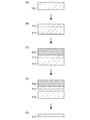
まず、ベース基板100と単結晶半導体基板110とを準備する(図1(A)、図1(B)参照)。
First, a
ベース基板100としては、絶縁体でなる基板を用いることができる。具体的には、アルミノシリケートガラス、アルミノホウケイ酸ガラス、バリウムホウケイ酸ガラスのような電子工業用に使われる各種ガラス基板、石英基板、セラミック基板、サファイア基板が挙げられる。なお、上記ガラス基板においては、一般に、ホウ酸(B2O3)を多く含有させることでガラスの耐熱性が向上するが、ホウ酸と比較して酸化バリウム(BaO)を多く含ませることで、より実用的な耐熱ガラスが得られる。このため、B2O3よりBaOを多く含むガラス基板を用いると良い。他にも、ベース基板100として単結晶半導体基板(例えば、単結晶シリコン基板等)を用いてもよい。本実施の形態では、ベース基板100としてガラス基板を用いる場合について説明する。ベース基板100として大面積化が可能で安価なガラス基板を用いることにより、低コスト化を図ることができる。
As the
上記ベース基板100に関しては、その表面をあらかじめ洗浄しておくことが好ましい。具体的には、ベース基板100に対して、塩酸過水(HPM)、硫酸過水(SPM)、アンモニア過水(APM)、希フッ酸(DHF)等を用いて超音波洗浄を行う。このような洗浄処理を行うことによって、ベース基板100表面の平坦性向上や、ベース基板100表面に残存する研磨粒子の除去などが可能である。
The surface of the
単結晶半導体基板110としては、例えば、単結晶シリコン基板、単結晶ゲルマニウム基板、単結晶シリコンゲルマニウム基板など、第14族元素でなる単結晶半導体基板を用いることができる。また、ガリウムヒ素やインジウムリン等の化合物単結晶半導体基板を用いることもできる。市販のシリコン基板としては、直径5インチ(125mm)、直径6インチ(150mm)、直径8インチ(200mm)、直径12インチ(300mm)、直径16インチ(400mm)サイズの円形のものが代表的である。なお、単結晶半導体基板110の形状は円形に限られず、例えば、矩形等に加工して用いることも可能である。また、単結晶半導体基板110は、CZ法やFZ(フローティングゾーン)法を用いて作製することができる。
As the single
なお、開示する発明の一態様は、単結晶半導体基板110の表層部分の結晶性や平坦性といった特徴を利用するものであるから、その表面の性質が、単結晶半導体基板と大きく変わらないものであれば上述の基板に限らず用いることができる。例えば、ガラス基板や石英基板、シリコン基板などの上に絶縁層を介して単結晶半導体層が設けられた構成の基板(いわゆるSOI基板など)を用いても良い。
Note that one embodiment of the disclosed invention utilizes characteristics such as crystallinity and flatness of a surface layer portion of the single
次に、単結晶半導体基板110上に、気相エピタキシャル成長法によって単結晶半導体層112を形成する(図1(C)参照)。
Next, a single
上記の単結晶半導体層112は、単結晶半導体基板110と同様の材料を用いて形成すれば良いが、例えば、単結晶シリコン層を形成する場合には、シラン系ガス(珪素の水素化合物を含むガス、代表的にはモノシランやジシラン)と水素との混合ガスを原料ガスとする気相成長法(CVD法などを含む)を用いて形成することができる。
The single
上記気相エピタキシャル成長に用いる原料ガスは、シラン系ガスに対して、流量比で4倍以上10倍以下、好ましくは5倍以上7倍以下の水素を含むガスを用いることが好ましい。つまり、シラン系ガスの水素希釈比(水素/シラン系ガス)を4倍以上10倍以下、好ましくは5倍以上7倍以下とする。シラン系ガスは代表的にはシランであり、その他ジシラン(Si2H6)などを用いることもできる。また、原料ガスに、希ガスを添加してもよい。 The source gas used for the vapor phase epitaxial growth is preferably a gas containing hydrogen having a flow rate ratio of 4 to 10 times, preferably 5 to 7 times that of the silane-based gas. That is, the hydrogen dilution ratio (hydrogen / silane-based gas) of the silane-based gas is 4 to 10 times, preferably 5 to 7 times. The silane-based gas is typically silane, and other disilane (Si 2 H 6 ) can also be used. Further, a rare gas may be added to the source gas.
エピタキシャル成長に使用するプラズマCVD装置としては、電力周波数が10MHz以上200MHz以下、代表的には13.56MHz或いは60MHzの高周波(RF)プラズマCVD装置や、電力周波数が1GHz以上5GHz以下、代表的には2.45GHzのマイクロ波プラズマCVD装置などを用いることができる。 As a plasma CVD apparatus used for epitaxial growth, a power frequency is 10 MHz to 200 MHz, typically a high frequency (RF) plasma CVD apparatus of 13.56 MHz or 60 MHz, a power frequency is 1 GHz to 5 GHz, typically 2 A 45 GHz microwave plasma CVD apparatus or the like can be used.
単結晶半導体層112の圧縮応力が高くなるような気相エピタキシャル成長の条件は適宜設定することができるが、一例としては、原料ガスとしてシランと水素の混合ガスを用い、シランと水素の流量(sccm)比をSiH4:H2=25(sccm):150(sccm)、基板温度を280℃、高周波電源の出力を30W、電力周波数を27MHzとすればよい。このような条件(特に流量比)で形成した単結晶半導体層112は圧縮応力が高く、単結晶半導体基板110との界面で容易に分離することができるようになる。なお、成膜の際の基板温度を200℃以上300℃以下程度とした場合には、欠陥の少ない良好な単結晶半導体層112を得ることができる。また、原料ガスの総流量を増大させることにより、成膜に掛かる時間を低減し、結晶性を向上させることが可能である。
The conditions of vapor phase epitaxial growth that can increase the compressive stress of the single
単結晶半導体層112の膜厚は、適宜必要な大きさとすればよいが、膜厚を増大させた場合にはそれに従って圧縮応力が大きくなる傾向にあるため、単結晶半導体基板110と単結晶半導体層112との界面での分離をより容易なものとすることができる。例えば、単結晶半導体層112の厚さは、100nm以上10μm以下程度とすればよい。
The film thickness of the single
なお、単結晶半導体層112のエピタキシャル成長を行う前には、単結晶半導体基板110表面に形成されている自然酸化膜などは除去しておく必要がある。これは、単結晶半導体基板110表面に酸化膜などが存在する場合には、エピタキシャル成長が進行しないためである。このような酸化膜の除去は、フッ酸系の溶液を用いて行うことができる。具体的には、フッ酸(又は希フッ酸)により単結晶半導体基板110の表面が撥水性を示すまで処理すればよい。同様に、汚染物除去の観点からは、硫酸過水(SPM)、アンモニア過水(APM)、塩酸過水(HPM)、希フッ酸(DHF)などを用いて単結晶半導体基板110の表面を洗浄しておくことが好ましい。
Note that a natural oxide film or the like formed over the surface of the single
次に、単結晶半導体層112上に、絶縁層114を形成する(図1(D)参照)。絶縁層114は、酸化シリコン膜、酸化窒化シリコン膜、窒化シリコン膜、窒化酸化シリコン膜等の絶縁層を単層で、又は積層させて形成することができる。これらの膜は、熱酸化法、CVD法、スパッタリング法等を用いて形成することができる。
Next, the insulating
本明細書中において、酸化窒化シリコンとは、その組成において、窒素よりも酸素の含有量が多いものを示し、例えば、酸素が50原子%以上70原子%以下、窒素が0.5原子%以上15原子%以下、珪素が25原子%以上35原子%以下、水素が0.1原子%以上10原子%以下の範囲で含まれるものをいう。また、窒化酸化シリコンとは、その組成において、酸素よりも窒素の含有量が多いものを示し、例えば、酸素が5原子%以上30原子%以下、窒素が20原子%以上55原子%以下、珪素が25原子%以上35原子%以下、水素が10原子%以上30原子%以下の範囲で含まれるものをいう。但し、上記範囲は、ラザフォード後方散乱法(RBS:Rutherford Backscattering Spectrometry)や、水素前方散乱法(HFS:Hydrogen Forward Scattering)を用いて測定した場合のものである。また、構成元素の含有比率の合計は、100原子%を超えない。 In this specification, silicon oxynitride refers to a silicon oxide having a higher oxygen content than nitrogen, for example, oxygen is 50 atomic% or more and 70 atomic% or less, and nitrogen is 0.5 atomic% or more. It includes 15 atomic percent or less, silicon in a range of 25 atomic percent to 35 atomic percent, and hydrogen in a range of 0.1 atomic percent to 10 atomic percent. Silicon nitride oxide refers to a composition having a nitrogen content higher than that of oxygen. For example, oxygen is 5 atomic% to 30 atomic%, nitrogen is 20 atomic% to 55 atomic%, silicon In the range of 25 atomic% to 35 atomic% and hydrogen in the range of 10 atomic% to 30 atomic%. However, the above ranges are those measured using Rutherford Backscattering Spectrometry (RBS) or Hydrogen Forward Scattering (HFS). Further, the total content ratio of the constituent elements does not exceed 100 atomic%.
なお、本実施の形態で示す半導体基板を、太陽電池など、下部電極が必要な用途に用いる場合には、単結晶半導体層112上に電極として機能する導電層を形成した後、上記の絶縁層114を形成する構成とすればよい。また、前述の導電層や絶縁層114を形成する前に、単結晶半導体層112には不純物を添加しておいても良い。
Note that in the case where the semiconductor substrate described in this embodiment is used for an application where a lower electrode is required, such as a solar battery, a conductive layer functioning as an electrode is formed over the single
その後、絶縁層114を介してベース基板100と単結晶半導体基板110とを貼り合わせる(図1(E)参照)。そして、単結晶半導体層112を単結晶半導体基板110との界面で分離して、ベース基板100上に単結晶半導体層112を設ける(図1(F)参照)。上記分離の方法として、基板分離装置などによる力学的方法(単純に引き剥がす方法)を用いることができる。また、ウォータージェットのように単結晶半導体層112と単結晶半導体基板110との界面に分離を促進させる処理を施す方法などを用いても良い。
After that, the
なお、ベース基板100と絶縁層114とを接合させた後には、接合強度を増加させるための熱処理を行っても良い。熱処理の温度は、適宜設定することができるが、高温(例えば600℃以上)の熱処理を行う場合には単結晶半導体基板110と単結晶半導体層112との接合が強化されてしまい、界面での分離が困難となることがある点に留意すべきである。上記熱処理には、拡散炉、抵抗加熱炉などの加熱炉、RTA(瞬間熱アニール、Rapid Thermal Anneal)装置、マイクロ波加熱装置などを用いることができる。
Note that heat treatment for increasing the bonding strength may be performed after the
以上の工程により、極めて良好な特性の半導体基板(SOI基板)を得ることができる。 Through the above steps, a semiconductor substrate (SOI substrate) with extremely good characteristics can be obtained.
なお、本実施の形態においては示していないが、上記の工程により得られた単結晶半導体層112に対して、レーザー光の照射処理を行っても良い。これにより、単結晶半導体層112中の欠陥をさらに低減し、表面の平坦性を向上させた単結晶半導体層を得ることができる。また、単結晶半導体層112に対して熱処理を施して、その欠陥を低減させても良い。
Although not shown in this embodiment mode, laser light irradiation treatment may be performed on the single
また、単結晶半導体層112の薄膜化のための処理や、平坦性をより一層向上させるための処理を行っても良い。該処理としては、ドライエッチングまたはウエットエッチングの一方、または双方を組み合わせて用いることができる。
Further, a process for reducing the thickness of the single
開示する発明の一態様では、気相エピタキシャル成長法によって形成された単結晶半導体層の応力を利用して、単結晶半導体基板から単結晶半導体層を分離している。これにより、単結晶半導体層自体には欠陥などが発生しないため、高温の熱処理が不要となる。また、分離後の単結晶半導体層は平坦性が高いため、CMP処理などの平坦化処理が不要となる。このように、開示する発明の一態様によって、特性が良好で且つ大面積な半導体基板(SOI基板)を提供することができる。 In one embodiment of the disclosed invention, the single crystal semiconductor layer is separated from the single crystal semiconductor substrate by using stress of the single crystal semiconductor layer formed by a vapor phase epitaxial growth method. Accordingly, no defects or the like are generated in the single crystal semiconductor layer itself, so that high-temperature heat treatment is unnecessary. Further, since the single crystal semiconductor layer after separation has high flatness, planarization treatment such as CMP treatment is not necessary. As described above, according to one embodiment of the disclosed invention, a semiconductor substrate (SOI substrate) with favorable characteristics and a large area can be provided.
また、開示する発明の一態様では、気相エピタキシャル成長法によって形成された単結晶半導体層を単結晶半導体基板との界面において分離する方法を用いているため、単結晶半導体基板自体の厚みは減少せず、単結晶半導体基板を繰り返して用いることができる。 In one embodiment of the disclosed invention, a method of separating a single crystal semiconductor layer formed by a vapor phase epitaxial growth method at an interface with the single crystal semiconductor substrate is used, so that the thickness of the single crystal semiconductor substrate itself is reduced. Instead, a single crystal semiconductor substrate can be used repeatedly.
本実施の形態で示した構成は、本明細書の他の実施の形態又は実施例で示す構成と適宜組み合わせて用いることができる。 The structure described in this embodiment can be combined as appropriate with any of the structures described in the other embodiments or examples in this specification.
(実施の形態2)
本実施の形態では、半導体基板(SOI基板)の作製方法の別の一例に関して図面を参照して説明する。
(Embodiment 2)
In this embodiment, another example of a method for manufacturing a semiconductor substrate (SOI substrate) will be described with reference to drawings.
まず、ベース基板100を準備する(図2(A)参照)。ベース基板100の詳細に関しては、実施の形態1を参照することができるため、ここでは省略する。
First, the
次に、ベース基板100の表面に窒素含有層102(例えば、窒化シリコン膜(SiNx)や窒化酸化シリコン膜(SiNxOy)(x>y)等の窒素を含有する絶縁膜)を形成する(図2(B)参照)。
Next, a nitrogen-containing layer 102 (for example, an insulating film containing nitrogen such as a silicon nitride film (SiN x ) or a silicon nitride oxide film (SiN x O y ) (x> y)) is formed on the surface of the
本実施の形態において形成される窒素含有層102は、後に単結晶半導体層を貼り合わせるための層(接合層)となる。また、窒素含有層102は、ベース基板に含まれるナトリウム(Na)等の不純物が単結晶半導体層に拡散することを防ぐためのバリア層として機能する。
The nitrogen-containing
上述のように、本実施の形態では窒素含有層102を接合層として用いるため、その表面が所定の平坦性を有するように窒素含有層102を形成することが好ましい。具体的には、表面の平均面粗さ(Ra)が0.5nm以下、自乗平均粗さ(Rms)が0.60nm以下、より好ましくは、平均面粗さが0.35nm以下、自乗平均粗さが0.45nm以下となるように窒素含有層102を形成する。膜厚は、好ましくは10nm以上200nm以下、より好ましくは50nm以上100nm以下の範囲とする。このように、表面の平坦性を高めておくことにより、単結晶半導体層の接合不良を防止することができる。
As described above, since the nitrogen-containing
次に、単結晶半導体基板110を準備する(図2(C)参照)。なお、本実施の形態においては、上記ベース基板100に関する工程の後に、以下の単結晶半導体基板110に関する工程を行う構成を取っているが、これは説明の便宜上のものであり、開示する発明の一態様がこの順序に限定して解釈されるものではない。また、単結晶半導体基板110の詳細に関しては、実施の形態1を参照することができるため、ここでは省略する。
Next, a single
次に、単結晶半導体基板110上に、気相エピタキシャル成長法によって単結晶半導体層112を形成する(図2(D)参照)。
Next, a single
上記の単結晶半導体層112として、例えば、単結晶シリコン層を形成する場合には、シラン系ガス(代表的にはシラン)と水素との混合ガスを原料ガスとする気相成長法(CVD法等を含む)を用いて形成することができる。単結晶半導体層112の作製方法の詳細については、実施の形態1を参照することができるため、ここでは省略する。
For example, in the case of forming a single crystal silicon layer as the single
次に、単結晶半導体層112上に、絶縁層114を形成する(図2(E)参照)。
Next, the insulating
絶縁層114は、例えば、酸化シリコン膜、酸化窒化シリコン膜等を単層で、又は積層させて形成することができる。上記絶縁層114の作製方法としては、熱酸化法、CVD法、スパッタリング法などがある。また、CVD法を用いて絶縁層114を形成する場合には、テトラエトキシシラン(略称;TEOS:化学式Si(OC2H5)4)等の有機シランを用いて酸化シリコン膜を形成することが、生産性の点から好ましい。
The insulating
本実施の形態では、絶縁層114として、有機シランを用いて酸化シリコン膜を形成する。
In this embodiment, a silicon oxide film is formed using organosilane as the insulating
なお、熱酸化法により絶縁層114を形成する場合には、酸化性雰囲気中にハロゲンを添加して行うことが好ましい。例えば、塩素(Cl)が添加された酸化性雰囲気中で単結晶半導体層112に熱酸化処理を行うことにより、塩素酸化された絶縁層114を形成することができる。この場合、絶縁層114は、塩素原子を含有した膜となる。
Note that when the insulating
絶縁層114中に含有された塩素原子等のハロゲンは、絶縁層114に歪みを形成する。その結果、絶縁層114の水分に対する吸収割合が向上し、拡散速度が増大する。つまり、絶縁層114表面に水分が存在する場合に、当該表面に存在する水分を絶縁層114中に素早く吸収させ、拡散させることができる。また、絶縁層114にハロゲンを含有させることによって、外因性不純物である重金属(例えば、Fe、Cr、Ni、Mo等)を絶縁層114中に捕集して単結晶半導体層112が汚染されることを防止できる。また、ベース基板100と貼り合わせた後に、ベース基板100からのNa等の不純物を絶縁層114中に固定して、単結晶半導体層112が汚染されることを防止できる。
A halogen such as a chlorine atom contained in the insulating
なお、本実施の形態で示す半導体基板を、太陽電池など、下部電極が必要な用途に用いる場合には、単結晶半導体層112上に電極として機能する導電層を形成した後、上記の絶縁層114を形成する構成とすればよい。また、前述の導電層や絶縁層114を形成する前に、単結晶半導体層112には不純物を添加しておいても良い。
Note that in the case where the semiconductor substrate described in this embodiment is used for an application where a lower electrode is required, such as a solar battery, a conductive layer functioning as an electrode is formed over the single
次に、ベース基板100の表面と単結晶半導体基板110の表面とを対向させ、窒素含有層102の表面と絶縁層114の表面とを接合させる(図2(F)参照)。
Next, the surface of the
ここでは、ベース基板100と単結晶半導体基板110を窒素含有層102と絶縁層114とを介して密着させた後、単結晶半導体基板110の一箇所に1N/cm2以上500N/cm2以下、好ましくは11N/cm2以上20N/cm2以下程度の圧力を加える。すると、圧力を加えた部分から窒素含有層102と絶縁層114とが接合しはじめ、自発的に接合が形成されて全面におよぶ。この接合工程には、ファンデルワールス力や水素結合が作用しており、常温で行うことができる。
Here, after the
なお、ベース基板100と単結晶半導体基板110との貼り合わせを行う前に、単結晶半導体基板110上に形成された絶縁層114と、ベース基板100上に形成された窒素含有層102の表面処理を行うことが好ましい。表面処理としては、プラズマ処理、オゾン処理、メガソニック洗浄、2流体洗浄(純水や水素添加水等の機能水を窒素等のキャリアガスとともに吹き付ける方法)又はこれらの組み合わせを用いることができる。特に、窒素含有層102、絶縁層114の少なくとも一方の表面にプラズマ処理を行った後、オゾン処理、メガソニック洗浄、2流体洗浄等を行うことによって、窒素含有層102や絶縁層114の表面の有機物等のゴミを除去し、親水化することができる。その結果、窒素含有層102と絶縁層114との接合強度を向上させることができる。
Note that the surface treatment of the insulating
ここで、オゾン処理の一例を説明する。例えば、酸素を含む雰囲気下で紫外線(UV)を照射することにより、被処理体表面にオゾン処理を行うことができる。酸素を含む雰囲気下で紫外線を照射するオゾン処理は、UVオゾン処理または紫外線オゾン処理などとも言われる。酸素を含む雰囲気下において、紫外線のうち200nm未満の波長を含む光と200nm以上の波長を含む光を照射することにより、オゾンを生成させるとともに、オゾンから一重項酸素を生成させることができる。紫外線のうち180nm未満の波長を含む光を照射することにより、オゾンを生成させるとともに、オゾンから一重項酸素を生成させることもできる。 Here, an example of ozone treatment will be described. For example, the surface of the object to be processed can be subjected to ozone treatment by irradiation with ultraviolet light (UV) in an atmosphere containing oxygen. Ozone treatment in which ultraviolet rays are irradiated in an atmosphere containing oxygen is also referred to as UV ozone treatment or ultraviolet ozone treatment. In an atmosphere containing oxygen, irradiation with light having a wavelength of less than 200 nm and light having a wavelength of 200 nm or more of ultraviolet light can generate ozone and singlet oxygen can be generated from ozone. By irradiating light including a wavelength of less than 180 nm among ultraviolet rays, ozone can be generated and singlet oxygen can be generated from ozone.
酸素を含む雰囲気下で、200nm未満の波長を含む光および200nm以上の波長を含む光を照射することにより起きる反応例を示す。
O2+hν(λ1nm)→O(3P)+O(3P) ・・・ (1)
O(3P)+O2→O3 ・・・ (2)
O3+hν(λ2nm)→O(1D)+O2 ・・・ (3)
An example of a reaction that occurs by irradiation with light having a wavelength of less than 200 nm and light having a wavelength of 200 nm or more in an atmosphere containing oxygen is shown.
O 2 + hν (λ 1 nm) → O ( 3 P) + O ( 3 P) (1)
O ( 3 P) + O 2 → O 3 (2)
O 3 + hν (λ 2 nm) → O ( 1 D) + O 2 (3)
上記反応式(1)において、酸素(O2)を含む雰囲気下で200nm未満の波長(λ1nm)を含む光(hν)を照射することにより基底状態の酸素原子(O(3P))が生成する。次に、反応式(2)において、基底状態の酸素原子(O(3P))と酸素(O2)とが反応してオゾン(O3)が生成する。そして、反応式(3)において、生成されたオゾン(O3)を含む雰囲気下で200nm以上の波長(λ2nm)を含む光が照射されることにより、励起状態の一重項酸素O(1D)が生成される。酸素を含む雰囲気下において、紫外線のうち200nm未満の波長を含む光を照射することによりオゾンを生成させるとともに、200nm以上の波長を含む光を照射することによりオゾンを分解して一重項酸素を生成する。上記のようなオゾン処理は、例えば、酸素を含む雰囲気下での低圧水銀ランプの照射(λ1=185nm、λ2=254nm)により行うことができる。 In the reaction formula (1), irradiation with light (hν) containing a wavelength (λ 1 nm) of less than 200 nm in an atmosphere containing oxygen (O 2 ) results in a ground state oxygen atom (O ( 3 P)). Produces. Next, in the reaction formula (2), the oxygen atom (O ( 3 P)) in the ground state reacts with oxygen (O 2 ) to generate ozone (O 3 ). Then, in reaction formula (3), irradiation with light including a wavelength (λ 2 nm) of 200 nm or more is performed in an atmosphere including the generated ozone (O 3 ), whereby singlet oxygen O ( 1 D) is generated. In an atmosphere containing oxygen, ozone is generated by irradiating light having a wavelength of less than 200 nm among ultraviolet rays, and singlet oxygen is generated by decomposing ozone by irradiating light having a wavelength of 200 nm or more. To do. The ozone treatment as described above can be performed, for example, by irradiation with a low-pressure mercury lamp (λ 1 = 185 nm, λ 2 = 254 nm) in an atmosphere containing oxygen.
また、酸素を含む雰囲気下で、180nm未満の波長を含む光を照射することにより起きる反応例を示す。
O2+hν(λ3nm)→O(1D)+O(3P) ・・・ (4)
O(3P)+O2→O3 ・・・ (5)
O3+hν(λ3nm)→O(1D)+O2 ・・・ (6)
An example of a reaction that occurs by irradiation with light having a wavelength of less than 180 nm in an oxygen-containing atmosphere is shown.
O 2 + hν (λ 3 nm) → O ( 1 D) + O ( 3 P) (4)
O ( 3 P) + O 2 → O 3 (5)
O 3 + hν (λ 3 nm) → O ( 1 D) + O 2 (6)
上記反応式(4)において、酸素(O2)を含む雰囲気下で180nm未満の波長(λ3nm)を含む光を照射することにより、励起状態の一重項酸素O(1D)と基底状態の酸素原子(O(3P))が生成する。次に、反応式(5)において、基底状態の酸素原子(O(3P))と酸素(O2)とが反応してオゾン(O3)が生成する。反応式(6)において、生成されたオゾン(O3)を含む雰囲気下で180nm未満の波長(λ3nm)を含む光が照射されることにより、励起状態の一重項酸素と酸素が生成される。酸素を含む雰囲気下において、紫外線のうち180nm未満の波長を含む光を照射することによりオゾンを生成させるとともにオゾンまたは酸素を分解して一重項酸素を生成する。上記のようなオゾン処理は、例えば、酸素を含む雰囲気下でのXeエキシマUVランプの照射(λ3=172nm)により行うことができる。 In the reaction formula (4), singlet oxygen O ( 1 D) and a ground state in an excited state are irradiated with light including a wavelength (λ 3 nm) of less than 180 nm in an atmosphere including oxygen (O 2 ). Of oxygen atoms (O ( 3 P)). Next, in reaction formula (5), oxygen atoms (O ( 3 P)) in the ground state and oxygen (O 2 ) react to generate ozone (O 3 ). In reaction formula (6), singlet oxygen and oxygen in an excited state are generated by irradiation with light having a wavelength of less than 180 nm (λ 3 nm) in an atmosphere including the generated ozone (O 3 ). The In an atmosphere containing oxygen, ozone is generated by irradiating light having a wavelength of less than 180 nm among ultraviolet rays, and ozone or oxygen is decomposed to generate singlet oxygen. The ozone treatment as described above can be performed, for example, by irradiation with a Xe excimer UV lamp (λ 3 = 172 nm) in an atmosphere containing oxygen.
200nm未満の波長を含む光により被処理体表面に付着する有機物などの化学結合を切断し、オゾンまたはオゾンから生成された一重項酸素により被処理体表面に付着する有機物、または化学結合を切断した有機物などを酸化分解して除去することができる。上記のようなオゾン処理を行うことで、被処理体表面の親水性および清浄性を高めることができ、接合を良好に行うことができる。 Chemical bonds such as organic substances adhering to the surface of the object to be processed are cut by light having a wavelength of less than 200 nm, and organic substances adhering to the surface of the object to be processed or chemical bonds are cut by singlet oxygen generated from ozone or ozone. Organic substances can be removed by oxidative decomposition. By performing the ozone treatment as described above, the hydrophilicity and cleanliness of the surface of the object to be processed can be improved, and bonding can be performed satisfactorily.
酸素を含む雰囲気下で紫外線を照射することによりオゾンが生成される。オゾンは、被処理体表面に付着する有機物の除去に効果を奏する。また、一重項酸素も、オゾンと同等またはそれ以上に、被処理体表面に付着する有機物の除去に効果を奏する。オゾン及び一重項酸素は、活性状態にある酸素の例であり、総称して活性酸素とも言われる。上記反応式等で説明したとおり、一重項酸素を生成する際にオゾンが生じる、またはオゾンから一重項酸素を生成する反応もあるため、ここでは一重項酸素が寄与する反応も含めて、便宜的にオゾン処理と称する。 Ozone is generated by irradiating ultraviolet rays in an atmosphere containing oxygen. Ozone is effective in removing organic substances adhering to the surface of the object to be processed. Singlet oxygen is also effective in removing organic substances adhering to the surface of the object to be processed, equivalent to or higher than ozone. Ozone and singlet oxygen are examples of oxygen in an active state, and are collectively referred to as active oxygen. As explained in the above reaction formulas and the like, ozone is generated when singlet oxygen is generated, or there is a reaction that generates singlet oxygen from ozone. This is called ozone treatment.
窒素含有層102と絶縁層114とを接合させた後には、接合強度を増加させるための熱処理を行っても良い。熱処理の温度は、適宜設定することができるが、高温(例えば600℃以上)の熱処理を行う場合には単結晶半導体基板110と単結晶半導体層112との接合が強化されてしまい、界面での分離が困難となることがある点に留意すべきである。上記熱処理には、拡散炉、抵抗加熱炉などの加熱炉、RTA(瞬間熱アニール、Rapid Thermal Anneal)装置、マイクロ波加熱装置などを用いることができる。
After the nitrogen-containing
その後、単結晶半導体層112を単結晶半導体基板110との界面で分離して、ベース基板100上に単結晶半導体層112を残存させる(図2(G)参照)。上記分離の方法として、基板分離装置などによる力学的方法(単純に引き剥がす方法)を用いることができる。また、ウォータージェットのように単結晶半導体層112と単結晶半導体基板110との界面に分離を促進させる処理を施す方法などを用いても良い。
After that, the single
以上の工程により、極めて良好な特性の半導体基板(SOI基板)を得ることができる。 Through the above steps, a semiconductor substrate (SOI substrate) with extremely good characteristics can be obtained.
なお、本実施の形態においては示していないが、上記の工程により得られた単結晶半導体層112に対して、レーザー光の照射処理を行っても良い。これにより、単結晶半導体層112中の欠陥をさらに低減し、表面の平坦性を向上させた単結晶半導体層を得ることができる。また、単結晶半導体層112に対して熱処理を施して、その欠陥を低減させても良い。
Although not shown in this embodiment mode, laser light irradiation treatment may be performed on the single
また、単結晶半導体層112の薄膜化のための処理や、平坦性を一層向上させるための処理を行っても良い。該処理としては、ドライエッチングまたはウエットエッチングの一方、または双方を組み合わせて用いることができる。
Alternatively, treatment for thinning the single
開示する発明の一態様では、気相エピタキシャル成長法によって形成された単結晶半導体層の応力を利用して、単結晶半導体基板から単結晶半導体層を分離している。これにより、単結晶半導体層自体には欠陥などが発生しないため、高温の熱処理が不要となる。また、分離後の単結晶半導体層は平坦性が高いため、CMP処理などの平坦化処理が不要となる。このように、開示する発明の一態様によって、特性が良好で且つ大面積な半導体基板(SOI基板)を提供することができる。 In one embodiment of the disclosed invention, the single crystal semiconductor layer is separated from the single crystal semiconductor substrate by using stress of the single crystal semiconductor layer formed by a vapor phase epitaxial growth method. Accordingly, no defects or the like are generated in the single crystal semiconductor layer itself, so that high-temperature heat treatment is unnecessary. Further, since the single crystal semiconductor layer after separation has high flatness, planarization treatment such as CMP treatment is not necessary. As described above, according to one embodiment of the disclosed invention, a semiconductor substrate (SOI substrate) with favorable characteristics and a large area can be provided.
また、開示する発明の一態様では、気相エピタキシャル成長法によって形成された単結晶半導体層を単結晶半導体基板との界面において分離する方法を用いているため、単結晶半導体基板自体の厚みは減少せず、単結晶半導体基板を繰り返して用いることができる。 In one embodiment of the disclosed invention, a method of separating a single crystal semiconductor layer formed by a vapor phase epitaxial growth method at an interface with the single crystal semiconductor substrate is used, so that the thickness of the single crystal semiconductor substrate itself is reduced. Instead, a single crystal semiconductor substrate can be used repeatedly.
本実施の形態で示した構成は、本明細書の他の実施の形態又は実施例で示す構成と適宜組み合わせて用いることができる。 The structure described in this embodiment can be combined as appropriate with any of the structures described in the other embodiments or examples in this specification.
(実施の形態3)
本実施の形態では、開示する発明の別の形態である単結晶半導体層の作製方法の一例に関して図面を参照して説明する。なお、本実施の形態に係る単結晶半導体層の作製方法は、実施の形態1や実施の形態2に係る半導体基板の作製方法を応用するものである。
(Embodiment 3)
In this embodiment, an example of a method for manufacturing a single crystal semiconductor layer, which is another embodiment of the disclosed invention, will be described with reference to drawings. Note that the method for manufacturing a semiconductor substrate according to Embodiment 1 or 2 is applied to the method for manufacturing a single crystal semiconductor layer according to this embodiment.
まず、単結晶半導体基板110を準備する(図3(A)参照)。単結晶半導体基板110の詳細については、実施の形態1などを参照することができるため、ここでは省略する。
First, a single
次に、単結晶半導体基板110上に、気相エピタキシャル成長法によって単結晶半導体層112を形成する(図3(B)参照)。単結晶半導体層112の作製方法の詳細についても、実施の形態1などを参照することができる。
Next, the single
次に、単結晶半導体基板110及び単結晶半導体層112を加熱し、所定の温度に保持した状態で、単結晶半導体層112上に金属を含有する材料を塗布(又はスクリーン印刷)して、金属層120を形成する(図3(C)参照)。加熱温度は、金属層120を形成することができる温度であれば特に限定されない。金属層120は、アルミニウムや銅などの材料を用いて形成することができる。なお、本実施の形態では塗布法(又はスクリーン印刷法)によって金属層120を形成しているが、開示する発明の一態様はこれに限定されない。スパッタリング法などの方法を用いて形成しても良い。
Next, in a state where the single
その後、単結晶半導体基板110、単結晶半導体層112及び金属層120を冷却することで、単結晶半導体基板110と単結晶半導体層112との界面において単結晶半導体基板110と単結晶半導体層112とを分離して、金属層120と単結晶半導体層112の積層構造体を形成する(図3(D)参照)。冷却温度は特に限定されないが、例えば、室温程度とすることができる。もちろん、室温より低い温度にまで冷却しても良い。
After that, the single
上記の方法で単結晶半導体基板110から単結晶半導体層112を分離することができるのは、単結晶半導体材料と金属材料の熱膨張係数が大きく異なるためである。この原理により、金属層120を形成する際の温度と冷却後の温度との差が大きいほど、良好な分離が実現できると言える。
The single
その後、金属層120を除去することで単結晶半導体層112(自立膜)を形成することができる(図3(E)参照)。なお、本実施の形態においては、最終的に金属層120を除去する構成を採用しているが、開示する発明の一態様はこれに限定されない。例えば、金属層120を電極などに利用する場合には、金属層120を除去せずに残存させる構成としても良い。また、形成された単結晶半導体層112は、そのまま用いても良いし、何らかの基板に貼り合わせて用いても良い。
After that, the
なお、本実施の形態においては示していないが、基板分離装置などによる力学的方法(単純に引き剥がす方法)や、ウォータージェットのような分離を促進させる方法などを上記分離の際に併用しても良い。 Although not shown in this embodiment, a mechanical method (a simple peeling method) using a substrate separation apparatus or a method for promoting separation such as a water jet is used in combination for the separation. Also good.
また、本実施の形態においては示していないが、上記の工程により得られた単結晶半導体層112に対して、レーザー光の照射処理を行っても良い。これにより、単結晶半導体層112中の欠陥をさらに低減し、表面の平坦性を向上させた単結晶半導体層を得ることができる。また、単結晶半導体層112に対して熱処理を施して、その欠陥を低減させても良い。
Although not shown in this embodiment mode, laser light irradiation treatment may be performed on the single
また、単結晶半導体層112の薄膜化のための処理や、平坦性を一層向上させるための処理を行っても良い。該処理としては、ドライエッチングまたはウエットエッチングの一方、または双方を組み合わせて用いることができる。
Alternatively, treatment for thinning the single
開示する発明の一態様では、気相エピタキシャル成長法によって形成された単結晶半導体層の応力を利用して、単結晶半導体基板から単結晶半導体層を分離している。これにより、単結晶半導体層自体には欠陥などが発生しないため、高温の熱処理が不要となる。また、分離後の単結晶半導体層は平坦性が高いため、CMP処理などの平坦化処理が不要となる。このように、開示する発明の一態様によって、特性が良好で且つ大面積な単結晶半導体層を提供することができる。 In one embodiment of the disclosed invention, the single crystal semiconductor layer is separated from the single crystal semiconductor substrate by using stress of the single crystal semiconductor layer formed by a vapor phase epitaxial growth method. Accordingly, no defects or the like are generated in the single crystal semiconductor layer itself, so that high-temperature heat treatment is unnecessary. Further, since the single crystal semiconductor layer after separation has high flatness, planarization treatment such as CMP treatment is not necessary. As described above, according to one embodiment of the disclosed invention, a single crystal semiconductor layer with favorable characteristics and a large area can be provided.
また、開示する発明の一態様では、気相エピタキシャル成長法によって形成された単結晶半導体層を単結晶半導体基板との界面において分離する方法を用いているため、単結晶半導体基板自体の厚みは減少せず、単結晶半導体基板を繰り返して用いることができる。 In one embodiment of the disclosed invention, a method of separating a single crystal semiconductor layer formed by a vapor phase epitaxial growth method at an interface with the single crystal semiconductor substrate is used, so that the thickness of the single crystal semiconductor substrate itself is reduced. Instead, a single crystal semiconductor substrate can be used repeatedly.
本実施の形態で示した構成は、本明細書の他の実施の形態又は実施例で示す構成と適宜組み合わせて用いることができる。 The structure described in this embodiment can be combined as appropriate with any of the structures described in the other embodiments or examples in this specification.
(実施の形態4)
本実施の形態では、単結晶半導体層の作製方法の別の一例に関して図面を参照して説明する。なお、本実施の形態に係る単結晶半導体層の作製方法は、実施の形態1や実施の形態2に係る半導体基板の作製方法を応用するものである。
(Embodiment 4)
In this embodiment, another example of a method for manufacturing a single crystal semiconductor layer will be described with reference to drawings. Note that the method for manufacturing a semiconductor substrate according to Embodiment 1 or 2 is applied to the method for manufacturing a single crystal semiconductor layer according to this embodiment.
まず、単結晶半導体基板110を準備する(図4(A)参照)。単結晶半導体基板110の詳細については、実施の形態1などを参照することができるため、ここでは省略する。
First, a single
次に、単結晶半導体基板110上に、気相エピタキシャル成長法によって単結晶半導体層112を形成する(図4(B)参照)。単結晶半導体層112の作製方法の詳細についても、実施の形態1などを参照することができる。なお、本実施の形態においては、単結晶半導体層112を十分に厚く形成する。具体的には5μm以上(100μm以下)の厚さで形成する。このように単結晶半導体層112を厚く形成することで、圧縮応力を十分に高めることができるため、単結晶半導体基板110と単結晶半導体層112の自発的な分離が可能になる(図4(C)および図4(D)参照)。また、単結晶半導体層112を十分に厚く形成することで、単結晶半導体層112を自立膜として分離することが可能になる。分離された単結晶半導体層112は、そのまま用いても良いし、何らかの基板に貼り合わせて用いても良い。
Next, a single
なお、本実施の形態においては示していないが、基板分離装置などによる力学的方法(単純に引き剥がす方法)や、ウォータージェットのような分離を促進させる方法などを上記分離の際に併用しても良い。 Although not shown in this embodiment, a mechanical method (a simple peeling method) using a substrate separation apparatus or a method for promoting separation such as a water jet is used in combination for the separation. Also good.
また、本実施の形態においては示していないが、上記の工程により得られた単結晶半導体層112に対して、レーザー光の照射処理を行っても良い。これにより、単結晶半導体層112中の欠陥をさらに低減し、表面の平坦性を向上させた単結晶半導体層を得ることができる。また、単結晶半導体層112に対して熱処理を施して、その欠陥を低減させても良い。
Although not shown in this embodiment mode, laser light irradiation treatment may be performed on the single
また、単結晶半導体層112の薄膜化のための処理や、平坦性を一層向上させるための処理を行っても良い。該処理としては、ドライエッチングまたはウエットエッチングの一方、または双方を組み合わせて用いることができる。
Alternatively, treatment for thinning the single
開示する発明の一態様では、気相エピタキシャル成長法によって形成された単結晶半導体層の応力を利用して、単結晶半導体基板から単結晶半導体層を分離している。これにより、単結晶半導体層自体には欠陥などが発生しないため、高温の熱処理が不要となる。また、分離後の単結晶半導体層は平坦性が高いため、CMP処理などの平坦化処理が不要となる。このように、開示する発明の一態様によって、特性が良好で且つ大面積な単結晶半導体層を提供することができる。 In one embodiment of the disclosed invention, the single crystal semiconductor layer is separated from the single crystal semiconductor substrate by using stress of the single crystal semiconductor layer formed by a vapor phase epitaxial growth method. Accordingly, no defects or the like are generated in the single crystal semiconductor layer itself, so that high-temperature heat treatment is unnecessary. Further, since the single crystal semiconductor layer after separation has high flatness, planarization treatment such as CMP treatment is not necessary. As described above, according to one embodiment of the disclosed invention, a single crystal semiconductor layer with favorable characteristics and a large area can be provided.
また、開示する発明の一態様では、気相エピタキシャル成長法によって形成された単結晶半導体層を単結晶半導体基板との界面において分離する方法を用いているため、単結晶半導体基板自体の厚みは減少せず、単結晶半導体基板を繰り返して用いることができる。 In one embodiment of the disclosed invention, a method of separating a single crystal semiconductor layer formed by a vapor phase epitaxial growth method at an interface with the single crystal semiconductor substrate is used, so that the thickness of the single crystal semiconductor substrate itself is reduced. Instead, a single crystal semiconductor substrate can be used repeatedly.
本実施の形態で示した構成は、本明細書の他の実施の形態又は実施例で示す構成と適宜組み合わせて用いることができる。 The structure described in this embodiment can be combined as appropriate with any of the structures described in the other embodiments or examples in this specification.
(実施の形態5)
本実施の形態では、図5乃至7を参照して、半導体装置の作製方法について説明する。ここでは、半導体装置の一例として複数のトランジスタからなる半導体装置の作製方法について説明することとする。なお、以下において示すトランジスタを組み合わせて用いることで、様々な半導体装置を作製することができる。
(Embodiment 5)
In this embodiment, a method for manufacturing a semiconductor device will be described with reference to FIGS. Here, a method for manufacturing a semiconductor device including a plurality of transistors is described as an example of the semiconductor device. Note that various semiconductor devices can be manufactured by using a combination of the transistors described below.
図5(A)は、実施の形態1により作製した半導体基板の断面図である。 FIG. 5A is a cross-sectional view of the semiconductor substrate manufactured according to Embodiment 1. FIG.
半導体層500(実施の形態1における単結晶半導体層112に対応)には、TFTのしきい値電圧を制御するために、硼素、アルミニウム、ガリウムなどのp型を付与する不純物元素、又はリン、砒素などのn型を付与する不純物元素を添加しても良い。不純物元素を添加する領域、および添加する不純物元素の種類は、適宜変更することができる。例えば、nチャネル型TFTの形成領域にp型を付与する不純物元素を添加し、pチャネル型TFTの形成領域にn型を付与する不純物元素を添加する。上述の不純物元素を添加する際には、ドーズ量が1×10¹⁵/cm2以上1×1017/cm2以下程度となるように行えばよい。その後、半導体層500を島状に分離して、半導体膜502、及び半導体膜504を形成する(図5(B)参照)。
In the semiconductor layer 500 (corresponding to the single
次に、半導体膜502と半導体膜504を覆うように、ゲート絶縁膜506を形成する(図5(C)参照)。ここでは、プラズマCVD法を用いて、酸化シリコン膜を単層で形成することとする。その他にも、酸化窒化シリコン、窒化酸化シリコン、窒化シリコン、酸化ハフニウム、酸化アルミニウム、酸化タンタル等を含む膜を、単層構造又は積層構造で形成することによりゲート絶縁膜506としても良い。
Next, a
プラズマCVD法以外の作製方法としては、スパッタリング法や、高密度プラズマ処理による酸化または窒化による方法が挙げられる。高密度プラズマ処理は、例えば、ヘリウム、アルゴン、クリプトン、キセノンなどの希ガスと、酸素、酸化窒素、アンモニア、窒素、水素などのガスの混合ガスを用いて行う。この場合、プラズマの励起をマイクロ波の導入により行うことで、低電子温度で高密度のプラズマを生成することができる。このような高密度のプラズマで生成された酸素ラジカル(OHラジカルを含む場合もある)や窒素ラジカル(NHラジカルを含む場合もある)によって、半導体膜の表面を酸化または窒化することにより、1nm以上20nm以下、望ましくは2nm以上10nm以下の絶縁膜を半導体膜に接するように形成する。 As a manufacturing method other than the plasma CVD method, a sputtering method or a method using oxidation or nitridation by high-density plasma treatment can be given. The high-density plasma treatment is performed using a mixed gas of a rare gas such as helium, argon, krypton, or xenon and a gas such as oxygen, nitrogen oxide, ammonia, nitrogen, or hydrogen. In this case, high-density plasma can be generated at a low electron temperature by exciting the plasma by introducing a microwave. By oxidizing or nitriding the surface of the semiconductor film with oxygen radicals (which may include OH radicals) or nitrogen radicals (which may include NH radicals) generated by such high-density plasma, 1 nm or more An insulating film having a thickness of 20 nm or less, preferably 2 nm or more and 10 nm or less is formed so as to be in contact with the semiconductor film.
上述した高密度プラズマ処理による半導体膜の酸化または窒化は固相反応であるため、ゲート絶縁膜506と半導体膜502及び半導体膜504との界面準位密度をきわめて低くすることができる。また、高密度プラズマ処理により半導体膜を直接酸化または窒化することで、形成される絶縁膜の厚さのばらつきを抑えることが出来る。また、半導体膜が単結晶であるため、高密度プラズマ処理を用いて半導体膜の表面を固相反応で酸化させる場合であっても、均一性が良く、界面準位密度の低いゲート絶縁膜を形成することができる。このように、高密度プラズマ処理により形成された絶縁膜をトランジスタのゲート絶縁膜の一部または全部に用いることで、特性のばらつきを抑制することができる。
Since the oxidation or nitridation of the semiconductor film by the high-density plasma treatment described above is a solid-phase reaction, the interface state density between the
又は、半導体膜502と半導体膜504を熱酸化させることで、ゲート絶縁膜506を形成するようにしても良い。このように、熱酸化を用いる場合には、ある程度の耐熱性を有するガラス基板を用いることが必要である。
Alternatively, the
なお、水素を含むゲート絶縁膜506を形成し、その後、350℃以上450℃以下の温度による加熱処理を行うことで、ゲート絶縁膜506中に含まれる水素を半導体膜502及び半導体膜504中に拡散させるようにしても良い。この場合、ゲート絶縁膜506として、プラズマCVD法を用いた窒化シリコン又は窒化酸化シリコンを用いることができる。なお、プロセス温度は350℃以下とすると良い。このように、半導体膜502及び半導体膜504に水素を供給することで、半導体膜502中、半導体膜504中、ゲート絶縁膜506と半導体膜502の界面、及びゲート絶縁膜506と半導体膜504の界面における欠陥を効果的に低減することができる。
Note that a
次に、ゲート絶縁膜506上に導電膜を形成した後、該導電膜を所定の形状に加工(パターニング)することで、半導体膜502の上方に電極508を、半導体膜504の上方に電極510を形成する(図5(D)参照)。導電膜の形成にはCVD法、スパッタリング法等を用いることができる。導電膜は、タンタル(Ta)、タングステン(W)、チタン(Ti)、モリブデン(Mo)、アルミニウム(Al)、銅(Cu)、クロム(Cr)、ニオブ(Nb)等の材料を用いて形成することができる。また、上記金属を主成分とする合金材料を用いても良いし、上記金属を含む化合物を用いても良い。または、半導体に導電性を付与する不純物元素をドーピングした多結晶シリコンなど、半導体材料を用いて形成しても良い。
Next, after a conductive film is formed over the
本実施の形態では電極508及び電極510を単層の導電膜で形成しているが、電極の構成はこれに限定されない。電極508及び電極510は積層された複数の導電膜で形成されていても良い。2層構造とする場合には、例えば、モリブデン膜、チタン膜、窒化チタン膜等を下層に用い、上層にはアルミニウム膜などを用いればよい。3層構造の場合には、モリブデン膜とアルミニウム膜とモリブデン膜の積層構造や、チタン膜とアルミニウム膜とチタン膜の積層構造などを採用するとよい。
In this embodiment mode, the
なお、電極508及び電極510を形成する際に用いるマスクは、酸化シリコンや窒化酸化シリコン等の材料を用いて形成してもよい。この場合、酸化シリコン膜や窒化酸化シリコン膜等をパターニングしてマスクを形成する工程が加わるが、レジスト材料と比較して、エッチング時におけるマスクの膜減りが少ないため、より正確な形状の電極508及び電極510を形成することができる。また、マスクを用いずに、液滴吐出法を用いて選択的に電極508及び電極510を形成しても良い。ここで、液滴吐出法とは、所定の組成物を含む液滴を吐出または噴出することで所定のパターンを形成する方法を意味し、インクジェット法などがその範疇に含まれる。
Note that a mask used for forming the
また、ICP(Inductively Coupled Plasma:誘導結合型プラズマ)エッチング法を用い、エッチング条件(コイル型の電極に印加される電力量、基板側の電極に印加される電力量、基板側の電極温度等)を適宜調節し、所望のテーパー形状を有するように導電膜をエッチングすることで、電極508及び電極510を形成することもできる。また、テーパー形状は、マスクの形状によって制御することもできる。なお、エッチング用ガスとしては、塩素、塩化硼素、塩化珪素、四塩化炭素などの塩素系ガス、四弗化炭素、弗化硫黄、弗化窒素などのフッ素系ガス、又は酸素などを適宜用いることができる。
In addition, using ICP (Inductively Coupled Plasma) etching method, etching conditions (amount of power applied to coil-type electrode, amount of power applied to substrate-side electrode, substrate-side electrode temperature, etc.) The
次に、電極508及び電極510をマスクとして、一導電型を付与する不純物元素を半導体膜502、半導体膜504に添加する(図6(A)参照)。本実施の形態では、半導体膜502にn型を付与する不純物元素(例えばリンまたはヒ素)を、半導体膜504にp型を付与する不純物元素(例えばボロン)を添加する。なお、n型を付与する不純物元素を半導体膜502に添加する際には、p型を付与する不純物元素が添加される半導体膜504はマスク等で覆い、n型を付与する不純物元素の添加が選択的に行われるようにする。また、p型を付与する不純物元素を半導体膜504に添加する際には、n型を付与する不純物元素が添加される半導体膜502はマスク等で覆い、p型を付与する不純物元素の添加が選択的に行われるようにする。又は、半導体膜502及び半導体膜504に、p型を付与する不純物元素又はn型を付与する不純物元素の一方を添加した後、一方の半導体膜のみに、より高い濃度でp型を付与する不純物元素又はn型を付与する不純物元素の他方を添加するようにしても良い。上記不純物元素の添加により、半導体膜502に不純物領域512、半導体膜504に不純物領域514が形成される。
Next, an impurity element imparting one conductivity type is added to the
次に、電極508の側面にサイドウォール516を、電極510の側面にサイドウォール518を形成する(図6(B)参照)。サイドウォール516及びサイドウォール518は、例えば、ゲート絶縁膜506、電極508及び電極510を覆うように新たに絶縁膜を形成し、垂直方向を主体とした異方性エッチングにより、該絶縁膜を部分的にエッチングすることで形成することができる。なお、上記の異方性エッチングにより、ゲート絶縁膜506を部分的にエッチングしても良い。サイドウォール516及びサイドウォール518を形成するための絶縁膜としては、プラズマCVD法やスパッタリング法等を用いて、シリコン、酸化シリコン、窒化シリコン、酸化窒化シリコン、窒化酸化シリコン、有機材料などを含む膜を、単層構造又は積層構造で形成すれば良い。本実施の形態では、膜厚100nmの酸化シリコン膜をプラズマCVD法によって形成する。また、エッチングガスとしては、CHF3とヘリウムの混合ガスを用いることができる。なお、サイドウォール516及びサイドウォール518を形成する工程は、これらに限定されるものではない。
Next, a
次に、ゲート絶縁膜506、電極508及び電極510、サイドウォール516及びサイドウォール518をマスクとして、半導体膜502、半導体膜504に一導電型を付与する不純物元素を添加する(図6(C)参照)。なお、半導体膜502、半導体膜504には、それぞれ先の工程で添加した不純物元素と同じ導電型の不純物元素をより高い濃度で添加する。ここで、n型を付与する不純物元素を半導体膜502に添加する際には、p型を付与する不純物元素が添加される半導体膜504はマスク等で覆い、n型を付与する不純物元素の添加が選択的に行われるようにする。また、p型を付与する不純物元素を半導体膜504に添加する際には、n型を付与する不純物元素が添加される半導体膜502はマスク等で覆い、p型を付与する不純物元素の添加が選択的に行われるようにする。
Next, an impurity element imparting one conductivity type is added to the
上記不純物元素の添加により、半導体膜502に、一対の高濃度不純物領域520と、一対の低濃度不純物領域522と、チャネル形成領域524とが形成される。また、上記不純物元素の添加により、半導体膜504に、一対の高濃度不純物領域526と、一対の低濃度不純物領域528と、チャネル形成領域530とが形成される。高濃度不純物領域520、高濃度不純物領域526はソース又はドレインとして機能し、低濃度不純物領域522、低濃度不純物領域528はLDD(Lightly Doped Drain)領域として機能する。
By the addition of the impurity element, a pair of high-
なお、半導体膜502上に形成されたサイドウォール516と、半導体膜504上に形成されたサイドウォール518は、キャリアが移動する方向(いわゆるチャネル長に平行な方向)の長さが同じになるように形成しても良いが、異なるように形成しても良い。pチャネル型トランジスタとなる半導体膜504上のサイドウォール518は、nチャネル型トランジスタとなる半導体膜502上のサイドウォール516よりも大きく形成すると良い。なぜならば、pチャネル型トランジスタにおいてソース及びドレインを形成するために注入されるボロンは拡散しやすく、短チャネル効果を誘起しやすいためである。pチャネル型トランジスタにおいて、サイドウォール518の長さをより大きくすることで、ソース及びドレインに高濃度のボロンを添加することが可能となり、ソース及びドレインを低抵抗化することができる。
Note that the
ソース及びドレインをさらに低抵抗化するために、半導体膜502及び半導体膜504の一部をシリサイド化したシリサイド層を形成しても良い。シリサイド化は、半導体膜に金属を接触させ、加熱処理(例えば、GRTA法、LRTA法等)により、半導体膜中の珪素と金属とを反応させて行う。シリサイド層としては、コバルトシリサイド又はニッケルシリサイドを用いれば良い。半導体膜502や半導体膜504が薄い場合には、半導体膜502、半導体膜504の底部までシリサイド反応を進めても良い。シリサイド化に用いることができる金属材料としては、チタン(Ti)、ニッケル(Ni)、タングステン(W)、モリブデン(Mo)、コバルト(Co)、ジルコニウム(Zr)、ハフニウム(Hf)、タンタル(Ta)、バナジウム(V)、ネオジム(Nd)、クロム(Cr)、白金(Pt)、パラジウム(Pd)等が挙げられる。また、レーザー光の照射などによってもシリサイド層を形成することができる。
In order to further reduce the resistance of the source and drain, a silicide layer in which part of the
上述の工程により、nチャネル型トランジスタ532及びpチャネル型トランジスタ534が形成される。なお、図6(C)に示す段階では、ソース電極又はドレイン電極として機能する導電膜は形成されていないが、これらのソース電極又はドレイン電極として機能する導電膜を含めてトランジスタと呼ぶこともある。
Through the above steps, an n-
次に、nチャネル型トランジスタ532、pチャネル型トランジスタ534を覆うように絶縁膜536を形成する(図6(D)参照)。絶縁膜536は必ずしも設ける必要はないが、絶縁膜536を形成することで、アルカリ金属やアルカリ土類金属などの不純物がnチャネル型トランジスタ532、pチャネル型トランジスタ534に侵入することを防止できる。具体的には、絶縁膜536を、酸化シリコン、窒化シリコン、酸化窒化シリコン、窒化酸化シリコン、窒化アルミニウム、酸化アルミニウムなどの材料を用いて形成するのが望ましい。本実施の形態では、膜厚600nm程度の窒化酸化シリコン膜を、絶縁膜536として用いる。なお、本実施の形態においては、絶縁膜536を単層構造としているが、積層構造としても良いことはいうまでもない。例えば、2層構造とする場合には、酸化窒化シリコン膜と窒化酸化シリコン膜との積層構造とすることができる。
Next, an insulating
次に、nチャネル型トランジスタ532、pチャネル型トランジスタ534を覆うように、絶縁膜536上に絶縁膜538を形成する。絶縁膜538は、ポリイミド、アクリル、ポリイミド、ベンゾシクロブテン、ポリアミド、エポキシ等の、耐熱性を有する有機材料を用いて形成するとよい。また、上記有機材料の他に、低誘電率材料(low−k材料)、シロキサン系樹脂、酸化シリコン、窒化シリコン、酸化窒化シリコン、窒化酸化シリコン、PSG(リンガラス)、BPSG(リンボロンガラス)、アルミナ等を用いることもできる。ここで、シロキサン系樹脂とは、シロキサン系材料を出発材料として形成されたSi−O−Si結合を含む樹脂に相当する。シロキサン系樹脂は、置換基に水素の他、フッ素、アルキル基、芳香族炭化水素から選ばれる一を有していても良い。なお、これらの材料で形成される絶縁膜を複数積層させることで、絶縁膜538を形成しても良い。
Next, an insulating
絶縁膜538の形成には、その材料に応じて、CVD法、スパッタ法、SOG法、スピンコート、ディップ、スプレー塗布、液滴吐出法(インクジェット法、スクリーン印刷、オフセット印刷等)、ドクターナイフ、ロールコーター、カーテンコーター、ナイフコーター等を用いることができる。
For the formation of the insulating
次に、半導体膜502と半導体膜504の一部が露出するように絶縁膜536及び絶縁膜538にコンタクトホールを形成する。そして、該コンタクトホールを介して半導体膜502に接する導電膜540及び導電膜542と、半導体膜504に接する導電膜544及び導電膜546を形成する(図7(A)参照)。導電膜540乃至導電膜546は、トランジスタのソース電極又はドレイン電極として機能する。なお、本実施の形態においては、コンタクトホール開口時のエッチングに用いるガスとしてCHF3とHeの混合ガスを用いることができるが、エッチングガスの種類はこれに限定されるものではない。
Next, contact holes are formed in the insulating
導電膜540乃至導電膜546は、CVD法やスパッタリング法等により形成することができる。具体的には、導電膜540乃至導電膜546として、アルミニウム(Al)、タングステン(W)、チタン(Ti)、タンタル(Ta)、モリブデン(Mo)、ニッケル(Ni)、白金(Pt)、銅(Cu)、金(Au)、銀(Ag)、マンガン(Mn)、ネオジム(Nd)、炭素(C)、珪素(Si)等を用いることができる。また、上記材料を主成分とする合金を用いても良いし、上記材料を含む化合物を用いても良い。また、導電膜540乃至導電膜546は、単層構造としても良いし、積層構造としても良い。
The
アルミニウムを主成分とする合金の例としては、アルミニウムを主成分として、ニッケルを含むものを挙げることができる。また、アルミニウムを主成分とし、ニッケルと、炭素または珪素の一方または両方を含むものを挙げることができる。アルミニウムやアルミニウムシリコン(Al−Si)は抵抗値が低く、安価であるため、導電膜540乃至導電膜546を形成する材料として適している。特に、アルミニウムシリコンは、パターニングの際のレジストベークによるヒロックの発生を抑制することができるため好ましい。また、珪素の代わりに、アルミニウムに0.5%程度のCuを混入させた材料を用いても良い。
As an example of an alloy containing aluminum as a main component, an alloy containing aluminum as a main component and containing nickel can be given. Further, examples include aluminum as a main component and one or both of nickel and carbon or silicon. Aluminum and aluminum silicon (Al—Si) have low resistance and are inexpensive, and thus are suitable as a material for forming the
導電膜540乃至導電膜546を積層構造とする場合には、例えば、バリア膜とアルミニウムシリコン膜とバリア膜の積層構造、バリア膜とアルミニウムシリコン膜と窒化チタン膜とバリア膜の積層構造などを採用するとよい。なお、バリア膜とは、チタン、チタンの窒化物、モリブデンまたはモリブデンの窒化物などを用いて形成された膜である。バリア膜の間にアルミニウムシリコン膜を挟むように導電膜を形成すると、アルミニウムやアルミニウムシリコンのヒロックの発生をより一層防止することができる。また、還元性の高い元素であるチタンを用いてバリア膜を形成すると、半導体膜502と半導体膜504上に薄い酸化膜が形成されていたとしても、バリア膜に含まれるチタンが該酸化膜を還元し、導電膜540及び導電膜542と半導体膜502とのコンタクト、導電膜544及び導電膜546と半導体膜504とのコンタクトを良好なものとすることができる。また、バリア膜を複数積層するようにして用いても良い。その場合、例えば、導電膜540乃至導電膜546を、下層からチタン、窒化チタン、アルミニウムシリコン、チタン、窒化チタンのように、5層構造又はそれ以上の積層構造とすることもできる。
In the case where the
また、導電膜540乃至導電膜546として、WF6ガスとSiH4ガスから化学気相成長法で形成したタングステンシリサイドを用いても良い。また、WF6を水素還元して形成したタングステンを、導電膜540乃至導電膜546として用いても良い。
Alternatively, tungsten silicide formed by a chemical vapor deposition method from WF 6 gas and SiH 4 gas may be used for the
なお、導電膜540及び導電膜542はnチャネル型トランジスタ532の高濃度不純物領域520に接続されている。導電膜544及び導電膜546はpチャネル型トランジスタ534の高濃度不純物領域526に接続されている。
Note that the
図7(B)に、図7(A)に示したnチャネル型トランジスタ532及びpチャネル型トランジスタ534の平面図を示す。ここで、図7(B)のA−Bにおける断面が図7(A)に対応している。ただし、図7(B)においては、簡単のため、導電膜540乃至導電膜546、絶縁膜536、絶縁膜538等を省略している。
FIG. 7B is a plan view of the n-
なお、本実施の形態においては、nチャネル型トランジスタ532とpチャネル型トランジスタ534が、それぞれゲート電極として機能する電極を1つずつ有する場合(電極508、電極510を有する場合)を例示しているが、トランジスタの構成はこれに限定されない。作製されるトランジスタは、ゲート電極として機能する電極を複数有し、なおかつ該複数の電極が電気的に接続されているマルチゲート構造を有していても良い。
Note that in this embodiment, the case where the n-
本実施の形態では、単結晶半導体層を用いてトランジスタを形成している。これにより、非晶質半導体層や非単結晶半導体層などを用いる場合と比較して、トランジスタのスイッチング速度が向上する。さらに、本実施の形態では、均質かつ良好な単結晶半導体層を用いているため、トランジスタ間の特性ばらつきを十分に抑制することができる。これにより、優れた特性の半導体装置を提供することができる。 In this embodiment, a transistor is formed using a single crystal semiconductor layer. Accordingly, the switching speed of the transistor is improved as compared with the case where an amorphous semiconductor layer, a non-single-crystal semiconductor layer, or the like is used. Further, in this embodiment, since a uniform and favorable single crystal semiconductor layer is used, variation in characteristics between transistors can be sufficiently suppressed. Thereby, a semiconductor device having excellent characteristics can be provided.
本実施の形態は、他の実施の形態又は実施例と適宜組み合わせて用いることができる。 This embodiment can be combined with any of the other embodiments or examples as appropriate.
(実施の形態6)
本実施の形態では、図8を参照して、光電変換装置(例えば、太陽電池)の作製方法について説明する。なお、以下においては、実施の形態1に示す方法を変形して作製した単結晶半導体層を用いて光電変換装置を作製する場合について説明する。
(Embodiment 6)
In this embodiment, a method for manufacturing a photoelectric conversion device (e.g., a solar cell) will be described with reference to FIGS. Note that a case where a photoelectric conversion device is manufactured using a single crystal semiconductor layer which is manufactured by modifying the method described in Embodiment 1 is described below.
はじめに、実施の形態1に示す例にしたがって、ベース基板800上に、絶縁層802、第1の導電層804、一導電型を示す第1の不純物半導体層806、不純物元素が(意図的には)添加されていない半導体層808、が順に積層された構造を形成する(図8(A)参照)。ここで、第1の不純物半導体層806と、半導体層808は、それぞれ、実施の形態1における単結晶半導体層112の一部である。すなわち、上記の構造は、実施の形態1において単結晶半導体層112上に絶縁層114を形成する前に、単結晶半導体層112に一導電型を示す不純物元素を添加し、その後、単結晶半導体層112上に第1の導電層804を形成し、該導電層804上に絶縁層114を形成することにより形成される。
First, in accordance with the example described in Embodiment 1, an insulating
上記一導電型は、n型、p型のいずれであっても良いが、本実施の形態においては、一導電型をn型とする場合について説明する。一導電型をn型とする場合には、リンやヒ素などの不純物元素を添加すればよい。また、p型とする場合には、ボロンなどを添加すればよい。 The one conductivity type may be either n-type or p-type. In this embodiment, the case where one conductivity type is n-type will be described. When one conductivity type is n-type, an impurity element such as phosphorus or arsenic may be added. In the case of p-type, boron or the like may be added.
第1の導電層804は、タンタル(Ta)、タングステン(W)、チタン(Ti)、モリブデン(Mo)、アルミニウム(Al)、金(Au)、銀(Ag)、銅(Cu)、クロム(Cr)、ニオブ(Nb)等の材料を用いて形成することができる。また、上記金属を主成分とする合金材料を用いても良いし、上記金属を含む化合物を用いても良い。なお、本実施の形態においては第1の導電層804を単層構造とする場合について説明しているが、積層構造を採用しても良い。積層構造とする場合には、例えば、アルミニウムなどの低抵抗材料を窒化チタンや窒化タンタルなどのバリア性の高い材料で挟んだ構造の導電層を用いることができる。 The first conductive layer 804 includes tantalum (Ta), tungsten (W), titanium (Ti), molybdenum (Mo), aluminum (Al), gold (Au), silver (Ag), copper (Cu), chromium ( It can be formed using a material such as Cr) or niobium (Nb). Alternatively, an alloy material containing the above metal as a main component or a compound containing the above metal may be used. Note that although the case where the first conductive layer 804 has a single-layer structure is described in this embodiment, a stacked structure may be employed. In the case of a stacked structure, for example, a conductive layer having a structure in which a low-resistance material such as aluminum is sandwiched between materials having high barrier properties such as titanium nitride or tantalum nitride can be used.
次に、上記半導体層808上に、第1の不純物半導体層806とは異なる導電型が付与された、第2の不純物半導体層810を形成する(図8(B)参照)。本実施の形態では、不純物元素としてボロンを添加し、p型を示す第2の不純物半導体層810を形成する。第2の不純物半導体層810は、CVD法などの方法を用いて作製することができる。
Next, a second
なお、第2の不純物半導体層810の厚さは20nm以上200nm以下程度、好ましくは50nm以上100nm以下程度とすることが好ましい。第2の不純物半導体層810を薄く形成することにより、第2の不純物半導体層810でのキャリアの再結合を防止できる。
Note that the thickness of the second
次に、第2の不純物半導体層810上に、光(特に上記半導体層808に吸収される波長の光)が透過する導電性材料を用いて、第2の導電層812を形成する(図8(C)参照)。第2の導電層812は必須ではないが、光電変換効率向上のためには設けることが好ましい。
Next, a second
その後、第1の導電層804上に設けられた第1の不純物半導体層806、半導体層808、第2の不純物半導体層810及び第2の導電層812をエッチングして、第1の導電層804の一部(好ましくは第1の導電層804端部)を露出させる(図8(D)参照)。
After that, the first
ここで、第1の導電層804の一部を露出させるのは、第1の導電層804と接続される電極や配線(補助電極や補助配線)を形成するためである。光電変換装置として機能させるためには、正極と負極に対応する導電層(電極)から電気エネルギーを取り出すことが必要となるが、第1の導電層804の上部は半導体層などに覆われており、第1の導電層804の下方にはベース基板800が設けられているため、このままでは電気エネルギーを取り出しにくい。そこで、第1の導電層804の上方に形成されている層の一部を除去し、第1の導電層804の一部を露出させ、引き回すことができる電極や配線(補助電極や補助配線)を形成できるようにする。
Here, part of the first conductive layer 804 is exposed in order to form an electrode or a wiring (auxiliary electrode or auxiliary wiring) connected to the first conductive layer 804. In order to function as a photoelectric conversion device, it is necessary to extract electric energy from the conductive layer (electrode) corresponding to the positive electrode and the negative electrode, but the upper portion of the first conductive layer 804 is covered with a semiconductor layer or the like. Since the
具体的には、第2の導電層812上にレジスト材料や窒化シリコンなどの絶縁材料を用いてマスクを形成し、該マスクを用いてエッチングを行えばよい。エッチングは、例えば、NF3、SF6などのフッ素系ガスを用いたドライエッチングとすることができ、少なくとも第1の導電層804と、第1の導電層804の上方に形成されている層(第1の不純物半導体層806、半導体層808、第2の不純物半導体層810、第2の導電層812)との選択比が充分に確保できる条件で行えばよい。なお、エッチング後には、不要となったマスクは除去する。
Specifically, a mask may be formed over the second
次に、露出させた第1の導電層804に接続する補助電極814、及び第2の導電層812に接続する電極816を形成する(図8(E)参照)。
Next, an
補助電極814は、光電変換された電気エネルギーを取り出しやすくするために設けられている。すなわち、補助電極814は取り出し電極(集電極とも言う)として機能する。
The
電極816は、平面図で見て格子状(或いは櫛状、櫛形、櫛歯状)となるように形成すると良い。このような形状とすることで、半導体層808などに十分な光を照射することができるため、光吸収効率を向上させることができる。もちろん、電極816の形状はこれに限定して解釈されるものではない。なお、電極816は補助電極814と同じ工程で形成される。
The
電極816や補助電極814は、アルミニウム、銀、鉛錫(半田)などを用いて、印刷法などの方法で形成すれば良い。例えば、銀ペーストを用いてスクリーン印刷法で形成することができる。
The
以上により、光電変換装置を作製することができる。なお、本実施の形態においては、光電変換に係る半導体層が単層(いわゆるシングルセル)の光電変換装置を作製する場合について説明しているが、光電変換装置の構成はこれに限定されない。光電変換に係る半導体層が二層の、所謂タンデムセルとしても良い。 Through the above steps, a photoelectric conversion device can be manufactured. Note that in this embodiment, the case where a photoelectric conversion device having a single layer (so-called single cell) semiconductor layer for photoelectric conversion is described; however, the structure of the photoelectric conversion device is not limited thereto. A so-called tandem cell having two semiconductor layers for photoelectric conversion may be used.
本実施の形態では、均質かつ良好な単結晶半導体層を用いて光電変換装置を作製しているため、変換効率の高い光電変換装置を作製することができる。本実施の形態は、他の実施の形態又は実施例と適宜組み合わせて用いることができる。 In this embodiment mode, a photoelectric conversion device is manufactured using a single crystal semiconductor layer that is homogeneous and favorable, and thus a photoelectric conversion device with high conversion efficiency can be manufactured. This embodiment can be combined with any of the other embodiments or examples as appropriate.
(実施の形態7)
本実施の形態では、図9を参照して、光電変換装置(例えば、太陽電池)の作製方法について説明する。なお、以下においては、実施の形態3又は実施の形態4に示す方法によって作製した単結晶半導体層を用いて光電変換装置を作製する場合について説明する。
(Embodiment 7)
In this embodiment, a method for manufacturing a photoelectric conversion device (for example, a solar cell) will be described with reference to FIGS. Note that the case where a photoelectric conversion device is manufactured using a single crystal semiconductor layer manufactured by the method described in Embodiment 3 or 4 will be described below.
はじめに、実施の形態3又は実施の形態4に示す方法にしたがって、単結晶半導体層900を用意する(図9(A)参照)。
First, a single
次に、ガス拡散法などを用いて、一導電型を示す不純物元素を単結晶半導体層900中に拡散させて、第1の不純物領域902を形成する(図9(B)参照)。上記一導電型は、n型、p型のいずれとしても良いが、本実施の形態においては、一導電型をn型とする場合について説明する。一導電型をn型とする場合には、リンやヒ素などの不純物元素を拡散させればよい。例えば、POCl3を拡散源として用いて、リンを拡散させることができる。なお、一導電型をp型とする場合には、ボロンなどを拡散させればよい。
Next, an impurity element having one conductivity type is diffused into the single
上記不純物元素を拡散させる前には、単結晶半導体層900の表面に凹凸構造(テクスチャ)を形成しても良い。表面に凹凸構造を形成する方法としては、エッチング処理などを適用することができる。このような表面凹凸構造を形成することにより、半導体層中への光閉じ込め効果によって光電変換効率を向上させることができる。
Before the impurity element is diffused, an uneven structure (texture) may be formed on the surface of the single
次に、第1の不純物領域902の一表面に、反射防止膜904を形成する(図9(C)参照)。反射防止膜904は酸化チタンなどの材料を用いて形成すればよい。作製方法としては、CVD法などを用いることができる。
Next, an
その後、受光面となる側(反射防止膜904が形成されている側)以外に存在する第1の不純物領域902を除去する(図9(D)参照)。除去方法としては、エッチング処理などを適用すればよい。
After that, the
次に、受光面の反対側に、裏面電極906を形成する(図9(E)参照)。裏面電極906は、タンタル(Ta)、タングステン(W)、チタン(Ti)、モリブデン(Mo)、アルミニウム(Al)、金(Au)、銀(Ag)、銅(Cu)、クロム(Cr)、ニオブ(Nb)等の材料を用いて形成することができる。本実施の形態においては、裏面電極906として、アルミニウム膜を形成する。作製方法としては、スクリーン印刷法やスパッタ法などがあるが、本実施の形態においてはスクリーン印刷法を用いることとする。 Next, a back electrode 906 is formed on the side opposite to the light receiving surface (see FIG. 9E). The back electrode 906 includes tantalum (Ta), tungsten (W), titanium (Ti), molybdenum (Mo), aluminum (Al), gold (Au), silver (Ag), copper (Cu), chromium (Cr), It can be formed using a material such as niobium (Nb). In this embodiment, an aluminum film is formed as the back electrode 906. As a manufacturing method, there are a screen printing method, a sputtering method, and the like. In this embodiment mode, a screen printing method is used.
なお、スクリーン印刷法でアルミニウム膜を形成する場合には、乾燥や焼成の処理の際に、単結晶半導体層900中にアルミニウムを拡散させて第2の不純物領域908を形成し、BSF(Back Surface Field)効果を得ることができる(図9(F)参照)。
Note that in the case of forming an aluminum film by a screen printing method, the second impurity region 908 is formed by diffusing aluminum in the single
そして、反射防止膜904の一部を除去して、受光面電極910を形成する。受光面電極910も裏面電極906と同様の材料を用いて形成すればよいが、ここでは、銀ペーストを用いたスクリーン印刷法によって受光面電極910を形成する。
Then, a part of the
以上により、光電変換装置を作製することができる。なお、本実施の形態においては、光電変換に係る半導体層が単層(いわゆるシングルセル)の光電変換装置を作製する場合について説明しているが、光電変換装置の構成はこれに限定されない。光電変換に係る半導体層が二層の、所謂タンデムセルとしても良い。 Through the above steps, a photoelectric conversion device can be manufactured. Note that in this embodiment, the case where a photoelectric conversion device having a single layer (so-called single cell) semiconductor layer for photoelectric conversion is described; however, the structure of the photoelectric conversion device is not limited thereto. A so-called tandem cell having two semiconductor layers for photoelectric conversion may be used.
本実施の形態では、均質かつ良好な単結晶半導体層を用いて光電変換装置を作製しているため、変換効率の高い光電変換装置を作製することができる。本実施の形態は、他の実施の形態又は実施例と適宜組み合わせて用いることができる。 In this embodiment mode, a photoelectric conversion device is manufactured using a single crystal semiconductor layer that is homogeneous and favorable, and thus a photoelectric conversion device with high conversion efficiency can be manufactured. This embodiment can be combined with any of the other embodiments or examples as appropriate.
(実施の形態8)
本実施の形態では、上記の実施の形態にて作製した半導体装置、特に表示装置を用いた電子機器について、図10及び図11を参照して説明する。
(Embodiment 8)
In this embodiment, electronic devices using the semiconductor device manufactured in the above embodiment, particularly a display device, will be described with reference to FIGS.
半導体装置(特に表示装置)を用いて作製される電子機器としては、ビデオカメラやデジタルカメラなどのカメラ、ゴーグル型ディスプレイ(ヘッドマウントディスプレイ)、ナビゲーションシステム、音響再生装置(カーオーディオコンポ等)、コンピュータ、ゲーム機器、携帯情報端末(モバイルコンピュータ、携帯電話、携帯型ゲーム機または電子書籍等)、記録媒体を備えた画像再生装置(具体的にはDigital Versatile Disc(DVD)等の記録媒体を再生し、その画像を表示しうるディスプレイを備えた装置)などが挙げられる。 Electronic devices manufactured using semiconductor devices (particularly display devices) include cameras such as video cameras and digital cameras, goggle-type displays (head-mounted displays), navigation systems, sound playback devices (car audio components, etc.), computers , A game device, a portable information terminal (mobile computer, mobile phone, portable game machine, electronic book, etc.), and an image playback device (specifically, Digital Versatile Disc (DVD)) provided with a recording medium. And a device provided with a display capable of displaying the image).
図10(A)はテレビ受像器又はパーソナルコンピュータのモニタである。筺体1601、支持台1602、表示部1603、スピーカー部1604、ビデオ入力端子1605等を含む。表示部1603には、開示する発明の一態様に係る半導体装置が用いられている。開示する発明の一態様により、信頼性が高く高性能なテレビ受像器又はパーソナルコンピュータのモニタを低価格で提供することができる。
FIG. 10A illustrates a television receiver or a personal computer monitor. A
図10(B)はデジタルカメラである。本体1611の正面部分には受像部1613が設けられており、本体1611の上面部分にはシャッターボタン1616が設けられている。また、本体1611の背面部分には、表示部1612、操作キー1614、及び外部接続ポート1615が設けられている。表示部1612には、開示する発明の一態様に係る半導体装置が用いられている。開示する発明の一態様により、信頼性が高く高性能なデジタルカメラを低価格で提供することができる。
FIG. 10B illustrates a digital camera. An
図10(C)はノート型パーソナルコンピュータである。本体1621には、キーボード1624、外部接続ポート1625、ポインティングデバイス1626が設けられている。また、本体1621には、表示部1623を有する筐体1622が取り付けられている。表示部1623には、開示する発明の一態様に係る半導体装置が用いられている。開示する発明の一態様により、信頼性が高く高性能なノート型パーソナルコンピュータを低価格で提供することができる。
FIG. 10C illustrates a laptop personal computer. A
図10(D)はモバイルコンピュータであり、本体1631、表示部1632、スイッチ1633、操作キー1634、赤外線ポート1635等を含む。表示部1632にはアクティブマトリクス表示装置が設けられている。表示部1632には、開示する発明の一態様に係る半導体装置が用いられている。開示する発明の一態様により、信頼性が高く高性能なモバイルコンピュータを低価格で提供することができる。
FIG. 10D illustrates a mobile computer, which includes a
図10(E)は画像再生装置である。本体1641には、表示部1644、記録媒体読み込み部1645及び操作キー1646が設けられている。また、本体1641には、スピーカー部1647及び表示部1643それぞれを有する筐体1642が取り付けられている。表示部1643及び表示部1644それぞれには、開示する発明の一態様に係る半導体装置が用いられている。開示する発明の一態様により、信頼性が高く高性能な画像再生装置を低価格で提供することができる。
FIG. 10E illustrates an image reproducing device. A
図10(F)は電子書籍である。本体1651には操作キー1653が設けられている。また、本体1651には複数の表示部1652が取り付けられている。表示部1652には、開示する発明の一態様に係る半導体装置が用いられている。開示する発明の一態様により、信頼性が高く高性能な電子書籍を低価格で提供することができる。
FIG. 10F illustrates an electronic book. The
図10(G)はビデオカメラであり、本体1661には外部接続ポート1664、リモコン受信部1665、受像部1666、バッテリー1667、音声入力部1668、操作キー1669が設けられている、また、本体1661には、表示部1662を有する筐体1663が取り付けられている。表示部1662には、開示する発明の一態様に係る半導体装置が用いられている。開示する発明の一態様により、信頼性が高く高性能なビデオカメラを低価格で提供することができる。
FIG. 10G illustrates a video camera. A
図10(H)は携帯電話であり、本体1671、筐体1672、表示部1673、音声入力部1674、音声出力部1675、操作キー1676、外部接続ポート1677、アンテナ1678等を含む。表示部1673には、開示する発明の一態様に係る半導体装置が用いられている。開示する発明の一態様により、信頼性が高く高性能な携帯電話を低価格で提供することができる。
FIG. 10H illustrates a mobile phone, which includes a
図11は、電話としての機能と、情報端末としての機能を併せ持った携帯電子機器1700の構成の一例である。ここで、図11(A)は正面図、図11(B)は背面図、図11(C)は展開図である。携帯電子機器1700は、電話と情報端末の双方の機能を備えており、音声通話以外にも様々なデータ処理が可能な、いわゆるスマートフォンと呼ばれる電子機器である。
FIG. 11 illustrates an example of a configuration of a portable
携帯電子機器1700は、筐体1701及び筐体1702で構成されている。筐体1701は、表示部1711、スピーカー1712、マイクロフォン1713、操作キー1714、ポインティングデバイス1715、カメラ用レンズ1716、外部接続端子1717等を備え、筐体1702は、キーボード1721、外部メモリスロット1722、カメラ用レンズ1723、ライト1724、イヤフォン端子1725等を備えている。また、アンテナは筐体1701内部に内蔵されている。上記構成に加えて、非接触ICチップ、小型記録装置等を内蔵していてもよい。
A portable
表示部1711には、開示する発明の一態様に係る半導体装置が組み込まれている。なお、表示部1711に表示される映像(及びその表示方向)は、携帯電子機器1700の使用形態に応じて様々に変化する。また、表示部1711と同一面にカメラ用レンズ1716を備えているため、映像を伴う音声通話(いわゆるテレビ電話)が可能である。なお、スピーカー1712及びマイクロフォン1713は音声通話に限らず、録音、再生等に用いることが可能である。カメラ用レンズ1723(及び、ライト1724)を用いて静止画及び動画の撮影を行う場合には、表示部1711はファインダーとして用いられることになる。操作キー1714は、電話の発信・着信、電子メール等の簡単な情報入力、画面のスクロール、表示部1711に表示されるカーソルの移動等に用いられる。
A semiconductor device according to one embodiment of the disclosed invention is incorporated in the
重なり合った筐体1701と筐体1702(図11(A))は、スライドし、図11(C)のように展開し、情報端末として使用できる。この場合には、キーボード1721、ポインティングデバイス1715を用いた円滑な操作が可能である。外部接続端子1717はACアダプタやUSBケーブル等の各種ケーブルと接続可能であり、充電やコンピュータ等とのデータ通信を可能にしている。また、外部メモリスロット1722に記録媒体を挿入し、より大容量のデータの保存及び移動に対応できる。上記機能に加えて、赤外線などの電磁波を用いた無線通信機能や、テレビ受信機能等を有していても良い。開示する発明の一態様により、信頼性が高く高性能な携帯電子機器を低価格で提供することができる。
The overlapping
以上の様に、開示する発明の適用範囲は極めて広く、あらゆる分野の電子機器に用いることが可能である。なお、本実施の形態は、他の実施の形態又は実施例と適宜組み合わせて用いることができる。 As described above, the application range of the disclosed invention is extremely wide and can be used for electronic devices in various fields. Note that this embodiment can be combined with any of the other embodiments or examples as appropriate.
本実施例では、単結晶半導体基板と気相エピタキシャル成長法によって得られた単結晶半導体層との界面において単結晶半導体層が分離される様子を確認した。なお、本実施例においては、単結晶半導体基板として単結晶シリコン基板を用いてサンプルを作製した。また、単結晶半導体層としては、シランと水素の流量(sccm)比をSiH4:H2=25(sccm):150(sccm)、基板温度を280℃、高周波電源の出力を30W、電力周波数を27MHzとしたプラズマCVD法によって単結晶シリコン層を形成した。 In this example, it was confirmed that the single crystal semiconductor layer was separated at the interface between the single crystal semiconductor substrate and the single crystal semiconductor layer obtained by the vapor phase epitaxial growth method. Note that in this example, a sample was manufactured using a single crystal silicon substrate as the single crystal semiconductor substrate. As the single crystal semiconductor layer, the flow rate (sccm) ratio between silane and hydrogen is SiH 4 : H 2 = 25 (sccm): 150 (sccm), the substrate temperature is 280 ° C., the output of the high-frequency power source is 30 W, and the power frequency A single crystal silicon layer was formed by a plasma CVD method with a frequency of 27 MHz.
上記サンプルの単結晶シリコン層表面に、ベース基板としてガラス基板を貼り合わせた。ここでは、簡易的に、接着剤を用いてガラス基板と単結晶シリコン層との貼り合わせを行っている。 A glass substrate as a base substrate was bonded to the surface of the single crystal silicon layer of the sample. Here, the glass substrate and the single crystal silicon layer are simply bonded using an adhesive.
貼り合わせ後に、単結晶シリコン基板とガラス基板とを引き剥がしたところ、ガラス基板側には単結晶シリコン層が残存した。また、単結晶シリコン基板の表面及び単結晶シリコン層の表面は十分に平坦であった。 After bonding, the single crystal silicon substrate and the glass substrate were peeled off, and a single crystal silicon layer remained on the glass substrate side. Further, the surface of the single crystal silicon substrate and the surface of the single crystal silicon layer were sufficiently flat.
以上により、単結晶シリコン基板と単結晶シリコン層との界面において単結晶シリコン層の分離が良好に行われる様子が確認できた。 From the above, it was confirmed that the single crystal silicon layer was well separated at the interface between the single crystal silicon substrate and the single crystal silicon layer.
なお、上記サンプルの単結晶シリコン層表面に粘着テープを貼り付けた後、単結晶シリコン基板から粘着テープを引き剥がした場合においても、上記と同様に、単結晶シリコン基板と単結晶シリコン層との界面において単結晶シリコン層の分離が良好に行われる様子が確認できた。 Even when the adhesive tape is peeled off from the single crystal silicon substrate after the adhesive tape has been applied to the surface of the single crystal silicon layer of the sample, the single crystal silicon substrate and the single crystal silicon layer are similar to the above. It was confirmed that the single crystal silicon layer was well separated at the interface.
本実施例で示した構成は、他の実施の形態と適宜組み合わせて用いることができる。 The structure described in this example can be used in appropriate combination with any of the other embodiments.
100 ベース基板
102 窒素含有層
110 単結晶半導体基板
112 単結晶半導体層
114 絶縁層
120 金属層
500 半導体層
502 半導体膜
504 半導体膜
506 ゲート絶縁膜
508 電極
510 電極
512 不純物領域
514 不純物領域
516 サイドウォール
518 サイドウォール
520 高濃度不純物領域
522 低濃度不純物領域
524 チャネル形成領域
526 高濃度不純物領域
528 低濃度不純物領域
530 チャネル形成領域
532 nチャネル型トランジスタ
534 pチャネル型トランジスタ
536 絶縁膜
538 絶縁膜
540 導電膜
542 導電膜
544 導電膜
546 導電膜
800 ベース基板
802 絶縁層
804 導電層
806 不純物半導体層
808 半導体層
810 不純物半導体層
812 導電層
814 補助電極
816 電極
900 単結晶半導体層
902 不純物領域
904 反射防止膜
906 裏面電極
908 不純物領域
910 受光面電極
1601 筺体
1602 支持台
1603 表示部
1604 スピーカー部
1605 ビデオ入力端子
1611 本体
1612 表示部
1613 受像部
1614 操作キー
1615 外部接続ポート
1616 シャッターボタン
1621 本体
1622 筐体
1623 表示部
1624 キーボード
1625 外部接続ポート
1626 ポインティングデバイス
1631 本体
1632 表示部
1633 スイッチ
1634 操作キー
1635 赤外線ポート
1641 本体
1642 筐体
1643 表示部
1644 表示部
1645 記録媒体読み込み部
1646 操作キー
1647 スピーカー部
1651 本体
1652 表示部
1653 操作キー
1661 本体
1662 表示部
1663 筐体
1664 外部接続ポート
1665 リモコン受信部
1666 受像部
1667 バッテリー
1668 音声入力部
1669 操作キー
1671 本体
1672 筐体
1673 表示部
1674 音声入力部
1675 音声出力部
1676 操作キー
1677 外部接続ポート
1678 アンテナ
1700 携帯電子機器
1701 筐体
1702 筐体
1711 表示部
1712 スピーカー
1713 マイクロフォン
1714 操作キー
1715 ポインティングデバイス
1716 カメラ用レンズ
1717 外部接続端子
1721 キーボード
1722 外部メモリスロット
1723 カメラ用レンズ
1724 ライト
1725 イヤフォン端子
100 Base substrate 102 Nitrogen-containing layer 110 Single crystal semiconductor substrate 112 Single crystal semiconductor layer 114 Insulating layer 120 Metal layer 500 Semiconductor layer 502 Semiconductor film 504 Semiconductor film 506 Gate insulating film 508 Electrode 510 Electrode 512 Impurity region 514 Impurity region 516 Side wall 518 Side wall 520 High concentration impurity region 522 Low concentration impurity region 524 Channel formation region 526 High concentration impurity region 528 Low concentration impurity region 530 Channel formation region 532 n-channel transistor 534 p-channel transistor 536 Insulating film 538 Insulating film 540 Conductive film 542 Conductive film 544 Conductive film 546 Conductive film 800 Base substrate 802 Insulating layer 804 Conductive layer 806 Impurity semiconductor layer 808 Semiconductor layer 810 Impurity semiconductor layer 812 Conductive layer 814 Auxiliary electrode 816 Electrode 900 Single crystal semiconductor layer 902 Impurity region 904 Antireflection film 906 Back surface electrode 908 Impurity region 910 Light receiving surface electrode 1601 Housing 1602 Display 1603 Display unit 1604 Speaker unit 1605 Video input terminal 1611 Main body 1612 Display unit 1613 Image receiving unit 1614 Operation key 1615 External connection port 1616 Shutter button 1621 Main body 1622 Case 1623 Display unit 1624 Keyboard 1625 External connection port 1626 Pointing device 1631 Main unit 1632 Display unit 1633 Switch 1634 Operation key 1635 Infrared port 1641 Main unit 1642 Case 1643 Display unit 1644 Display unit 1645 Recording medium Reading unit 1646 Operation key 1647 Speaker unit 1651 Main unit 1652 Display unit 1653 Operation key 1661 Main unit 662 Display unit 1663 Case 1664 External connection port 1665 Remote control receiver 1666 Image receiving unit 1667 Battery 1668 Audio input unit 1669 Operation key 1671 Main body 1672 Display unit 1673 Audio input unit 1675 Audio output unit 1676 Operation key 1677 External connection port 1678 Antenna 1700 Portable electronic device 1701 Case 1702 Case 1711 Display unit 1712 Speaker 1713 Microphone 1714 Operation key 1715 Pointing device 1716 Camera lens 1717 External connection terminal 1721 Keyboard 1722 External memory slot 1723 Camera lens 1724 Light 1725 Earphone terminal
Claims (4)
絶縁層を介して前記単結晶シリコン層とベース基板とを貼り合わせ、
前記単結晶シリコン基板と前記単結晶シリコン層との界面において、これらを分離して、前記ベース基板上に前記絶縁層を介して前記単結晶シリコン層を形成し、
前記単結晶シリコン層は、シランと水素との混合ガスを原料ガスとして用いて形成され、
前記原料ガスにおいて、前記シランに対する前記水素の流量比を4倍以上10倍以下とすることを特徴とするSOI基板の作製方法。 A single crystal silicon layer having a compressive stress is formed on the surface of the single crystal silicon substrate by vapor phase epitaxial growth at a substrate temperature of 200 ° C. or more and 300 ° C. or less, an output of a high frequency power supply of 30 W, and a power frequency of 27 MHz ,
Bonding the single crystal silicon layer and the base substrate through an insulating layer,
Separating them at the interface between the single crystal silicon substrate and the single crystal silicon layer, and forming the single crystal silicon layer on the base substrate via the insulating layer;
The single crystal silicon layer is formed using a mixed gas of Sila emissions and hydrogen as material gas,
Wherein the raw material gas, a method for manufacturing an SOI substrate, characterized by the following 10 times 4 times or more the flow rate of the hydrogen against the Sila down.
前記ベース基板として、ガラス基板を用いることを特徴とするSOI基板の作製方法。 In claim 1,
A method for manufacturing an SOI substrate, wherein a glass substrate is used as the base substrate.
前記単結晶シリコン基板及び前記単結晶シリコン層を加熱処理によって所定の温度に保持した状態で、前記単結晶シリコン層上に金属を含有する材料を塗布して金属層を形成し、
前記単結晶シリコン基板、前記単結晶シリコン層及び前記金属層を冷却することにより、前記単結晶シリコン基板と前記単結晶シリコン層との界面において、これらを分離して、前記金属層と前記単結晶シリコン層の積層構造体を形成し、
前記積層構造体から前記金属層を除去し、
前記単結晶シリコン層は、シランと水素との混合ガスを原料ガスとして用いて形成され、
前記原料ガスにおいて、前記シランに対する前記水素の流量比を4倍以上10倍以下とすることを特徴とする単結晶シリコン層の作製方法。 A single crystal silicon layer having a compressive stress is formed on the surface of the single crystal silicon substrate by vapor phase epitaxial growth at a substrate temperature of 200 ° C. or more and 300 ° C. or less, an output of a high frequency power supply of 30 W, and a power frequency of 27 MHz ,
In a state where the single crystal silicon substrate and the single crystal silicon layer are maintained at a predetermined temperature by heat treatment, a metal-containing material is applied on the single crystal silicon layer to form a metal layer,
By cooling the single crystal silicon substrate, the single crystal silicon layer, and the metal layer, the metal layer and the single crystal are separated at the interface between the single crystal silicon substrate and the single crystal silicon layer. Forming a laminated structure of silicon layers,
Removing the metal layer from the laminated structure;
The single crystal silicon layer is formed using a mixed gas of Sila emissions and hydrogen as material gas,
Wherein the raw material gas, a method of producing a single-crystal silicon layer, characterized in that less than 10 times 4 times or more the flow rate of the hydrogen against the Sila down.
前記金属を含有する材料として、アルミニウム又は銅を含む材料を用いることを特徴とする単結晶シリコン層の作製方法。 In claim 3,
A method for manufacturing a single crystal silicon layer, wherein a material containing aluminum or copper is used as the metal-containing material.
Priority Applications (1)
| Application Number | Priority Date | Filing Date | Title |
|---|---|---|---|
| JP2009219954A JP5705426B2 (en) | 2008-09-29 | 2009-09-25 | Method for manufacturing SOI substrate and method for manufacturing single crystal silicon layer |
Applications Claiming Priority (3)
| Application Number | Priority Date | Filing Date | Title |
|---|---|---|---|
| JP2008250114 | 2008-09-29 | ||
| JP2008250114 | 2008-09-29 | ||
| JP2009219954A JP5705426B2 (en) | 2008-09-29 | 2009-09-25 | Method for manufacturing SOI substrate and method for manufacturing single crystal silicon layer |
Publications (3)
| Publication Number | Publication Date |
|---|---|
| JP2010103514A JP2010103514A (en) | 2010-05-06 |
| JP2010103514A5 JP2010103514A5 (en) | 2012-10-18 |
| JP5705426B2 true JP5705426B2 (en) | 2015-04-22 |
Family
ID=42057900
Family Applications (1)
| Application Number | Title | Priority Date | Filing Date |
|---|---|---|---|
| JP2009219954A Expired - Fee Related JP5705426B2 (en) | 2008-09-29 | 2009-09-25 | Method for manufacturing SOI substrate and method for manufacturing single crystal silicon layer |
Country Status (2)
| Country | Link |
|---|---|
| US (1) | US8048754B2 (en) |
| JP (1) | JP5705426B2 (en) |
Families Citing this family (8)
| Publication number | Priority date | Publication date | Assignee | Title |
|---|---|---|---|---|
| JP5611571B2 (en) | 2008-11-27 | 2014-10-22 | 株式会社半導体エネルギー研究所 | Method for manufacturing semiconductor substrate and method for manufacturing semiconductor device |
| JP5755931B2 (en) * | 2010-04-28 | 2015-07-29 | 株式会社半導体エネルギー研究所 | Method for producing semiconductor film, method for producing electrode, method for producing secondary battery, and method for producing solar cell |
| FR2967813B1 (en) * | 2010-11-18 | 2013-10-04 | Soitec Silicon On Insulator | METHOD FOR PRODUCING A BENTALLIC METAL LAYER STRUCTURE |
| US20130247967A1 (en) * | 2012-03-23 | 2013-09-26 | Scott Harrington | Gaseous ozone (o3) treatment for solar cell fabrication |
| FR2995444B1 (en) | 2012-09-10 | 2016-11-25 | Soitec Silicon On Insulator | METHOD FOR DETACHING A LAYER |
| US20160300967A1 (en) * | 2013-03-19 | 2016-10-13 | Choshu Industry Co., Ltd. | Photovoltaic device |
| JP2019114572A (en) * | 2016-05-09 | 2019-07-11 | 株式会社カネカ | Manufacturing method of stacked photoelectric conversion device |
| EP4016699A1 (en) * | 2020-12-17 | 2022-06-22 | Volvo Car Corporation | Temperature management system |
Family Cites Families (23)
| Publication number | Priority date | Publication date | Assignee | Title |
|---|---|---|---|---|
| FR2681472B1 (en) | 1991-09-18 | 1993-10-29 | Commissariat Energie Atomique | PROCESS FOR PRODUCING THIN FILMS OF SEMICONDUCTOR MATERIAL. |
| DE69334324D1 (en) | 1992-01-30 | 2010-05-06 | Canon Kk | Production method for semiconductor substrate |
| JP2994837B2 (en) | 1992-01-31 | 1999-12-27 | キヤノン株式会社 | Semiconductor substrate flattening method, semiconductor substrate manufacturing method, and semiconductor substrate |
| JP3085184B2 (en) | 1996-03-22 | 2000-09-04 | 住友金属工業株式会社 | SOI substrate and manufacturing method thereof |
| JPH1093122A (en) | 1996-09-10 | 1998-04-10 | Nippon Telegr & Teleph Corp <Ntt> | Method of manufacturing thin-film solar cell |
| JP3697052B2 (en) * | 1997-03-26 | 2005-09-21 | キヤノン株式会社 | Substrate manufacturing method and semiconductor film manufacturing method |
| US6251754B1 (en) | 1997-05-09 | 2001-06-26 | Denso Corporation | Semiconductor substrate manufacturing method |
| JP3864495B2 (en) | 1997-05-15 | 2006-12-27 | 株式会社デンソー | Manufacturing method of semiconductor substrate |
| JPH1197379A (en) | 1997-07-25 | 1999-04-09 | Denso Corp | Semiconductor substrate and its manufacture |
| US6534380B1 (en) * | 1997-07-18 | 2003-03-18 | Denso Corporation | Semiconductor substrate and method of manufacturing the same |
| JP3921823B2 (en) | 1998-07-15 | 2007-05-30 | 信越半導体株式会社 | Manufacturing method of SOI wafer and SOI wafer |
| JP4476390B2 (en) * | 1998-09-04 | 2010-06-09 | 株式会社半導体エネルギー研究所 | Method for manufacturing semiconductor device |
| FR2817394B1 (en) * | 2000-11-27 | 2003-10-31 | Soitec Silicon On Insulator | METHOD FOR MANUFACTURING A SUBSTRATE, IN PARTICULAR FOR OPTICS, ELECTRONICS OR OPTOELECTRONICS AND SUBSTRATE OBTAINED THEREBY |
| JP4296726B2 (en) | 2001-06-29 | 2009-07-15 | 株式会社Sumco | Manufacturing method of semiconductor substrate and manufacturing method of field effect transistor |
| JP4771510B2 (en) * | 2004-06-23 | 2011-09-14 | キヤノン株式会社 | Semiconductor layer manufacturing method and substrate manufacturing method |
| JP2006216896A (en) * | 2005-02-07 | 2006-08-17 | Canon Inc | Solar cell manufacturing method |
| JP2007123858A (en) * | 2005-09-29 | 2007-05-17 | Sumitomo Chemical Co Ltd | Manufacturing method of group iii-v nitride semiconductor |
| JP2008277477A (en) * | 2007-04-27 | 2008-11-13 | Fujitsu Microelectronics Ltd | Semiconductor substrate and manufacturing method therefor |
| US7790563B2 (en) * | 2007-07-13 | 2010-09-07 | Semiconductor Energy Laboratory Co., Ltd. | Semiconductor device, electronic device and method for manufacturing semiconductor device |
| US7795114B2 (en) | 2007-08-10 | 2010-09-14 | Semiconductor Energy Laboratory Co., Ltd. | Manufacturing methods of SOI substrate and semiconductor device |
| US7781308B2 (en) | 2007-12-03 | 2010-08-24 | Semiconductor Energy Laboratory Co., Ltd. | Method for manufacturing SOI substrate |
| CN101504930B (en) | 2008-02-06 | 2013-10-16 | 株式会社半导体能源研究所 | Manufacturing method of SOI substrate |
| JP5611571B2 (en) | 2008-11-27 | 2014-10-22 | 株式会社半導体エネルギー研究所 | Method for manufacturing semiconductor substrate and method for manufacturing semiconductor device |
-
2009
- 2009-09-23 US US12/564,973 patent/US8048754B2/en not_active Expired - Fee Related
- 2009-09-25 JP JP2009219954A patent/JP5705426B2/en not_active Expired - Fee Related
Also Published As
| Publication number | Publication date |
|---|---|
| US8048754B2 (en) | 2011-11-01 |
| JP2010103514A (en) | 2010-05-06 |
| US20100081254A1 (en) | 2010-04-01 |
Similar Documents
| Publication | Publication Date | Title |
|---|---|---|
| JP5705426B2 (en) | Method for manufacturing SOI substrate and method for manufacturing single crystal silicon layer | |
| JP5611571B2 (en) | Method for manufacturing semiconductor substrate and method for manufacturing semiconductor device | |
| JP5500914B2 (en) | Laser irradiation device | |
| JP5433220B2 (en) | Semiconductor device and manufacturing method thereof | |
| TWI517214B (en) | Method for manufacturing microcrystalline semiconductor film and method for manufacturing semiconductor device | |
| JP2009278073A (en) | Semiconductor device, and method for manufacturing the same | |
| JP5823821B2 (en) | Method for manufacturing microcrystalline semiconductor film and method for manufacturing semiconductor device | |
| JP5774410B2 (en) | Method for manufacturing microcrystalline semiconductor film and method for manufacturing semiconductor device | |
| JP5709579B2 (en) | Method for manufacturing microcrystalline semiconductor film | |
| TW201230906A (en) | Wiring board, semiconductor device, and manufacturing methods thereof | |
| JP2009260312A (en) | Method for manufacturing soi substrate and method for manufacturing semiconductor device | |
| JP5586906B2 (en) | Method for manufacturing semiconductor device | |
| JP5503995B2 (en) | Method for manufacturing semiconductor device | |
| JP5866088B2 (en) | Method for manufacturing SOI substrate | |
| JP5925440B2 (en) | Method for manufacturing SOI substrate and method for manufacturing semiconductor device | |
| JP2010103505A (en) | Method for manufacturing soi substrate | |
| JP5576617B2 (en) | Method for evaluating crystallinity of single crystal semiconductor layer | |
| JP2009212387A (en) | Method of manufacturing semiconductor substrate |
Legal Events
| Date | Code | Title | Description |
|---|---|---|---|
| A521 | Request for written amendment filed |
Free format text: JAPANESE INTERMEDIATE CODE: A523 Effective date: 20120903 |
|
| A621 | Written request for application examination |
Free format text: JAPANESE INTERMEDIATE CODE: A621 Effective date: 20120903 |
|
| A977 | Report on retrieval |
Free format text: JAPANESE INTERMEDIATE CODE: A971007 Effective date: 20131226 |
|
| A131 | Notification of reasons for refusal |
Free format text: JAPANESE INTERMEDIATE CODE: A131 Effective date: 20140121 |
|
| A521 | Request for written amendment filed |
Free format text: JAPANESE INTERMEDIATE CODE: A523 Effective date: 20140318 |
|
| A131 | Notification of reasons for refusal |
Free format text: JAPANESE INTERMEDIATE CODE: A131 Effective date: 20140819 |
|
| A521 | Request for written amendment filed |
Free format text: JAPANESE INTERMEDIATE CODE: A523 Effective date: 20140908 |
|
| TRDD | Decision of grant or rejection written | ||
| A01 | Written decision to grant a patent or to grant a registration (utility model) |
Free format text: JAPANESE INTERMEDIATE CODE: A01 Effective date: 20150217 |
|
| A61 | First payment of annual fees (during grant procedure) |
Free format text: JAPANESE INTERMEDIATE CODE: A61 Effective date: 20150225 |
|
| R150 | Certificate of patent or registration of utility model |
Ref document number: 5705426 Country of ref document: JP Free format text: JAPANESE INTERMEDIATE CODE: R150 |
|
| LAPS | Cancellation because of no payment of annual fees |