JP5679397B2 - Method for manufacturing thin film transistor substrate - Google Patents
Method for manufacturing thin film transistor substrate Download PDFInfo
- Publication number
- JP5679397B2 JP5679397B2 JP2007265748A JP2007265748A JP5679397B2 JP 5679397 B2 JP5679397 B2 JP 5679397B2 JP 2007265748 A JP2007265748 A JP 2007265748A JP 2007265748 A JP2007265748 A JP 2007265748A JP 5679397 B2 JP5679397 B2 JP 5679397B2
- Authority
- JP
- Japan
- Prior art keywords
- metal layer
- photoresist pattern
- film transistor
- thin film
- forming
- Prior art date
- Legal status (The legal status is an assumption and is not a legal conclusion. Google has not performed a legal analysis and makes no representation as to the accuracy of the status listed.)
- Active
Links
Images


Classifications
-
- G—PHYSICS
- G02—OPTICS
- G02F—OPTICAL DEVICES OR ARRANGEMENTS FOR THE CONTROL OF LIGHT BY MODIFICATION OF THE OPTICAL PROPERTIES OF THE MEDIA OF THE ELEMENTS INVOLVED THEREIN; NON-LINEAR OPTICS; FREQUENCY-CHANGING OF LIGHT; OPTICAL LOGIC ELEMENTS; OPTICAL ANALOGUE/DIGITAL CONVERTERS
- G02F1/00—Devices or arrangements for the control of the intensity, colour, phase, polarisation or direction of light arriving from an independent light source, e.g. switching, gating or modulating; Non-linear optics
- G02F1/01—Devices or arrangements for the control of the intensity, colour, phase, polarisation or direction of light arriving from an independent light source, e.g. switching, gating or modulating; Non-linear optics for the control of the intensity, phase, polarisation or colour
- G02F1/13—Devices or arrangements for the control of the intensity, colour, phase, polarisation or direction of light arriving from an independent light source, e.g. switching, gating or modulating; Non-linear optics for the control of the intensity, phase, polarisation or colour based on liquid crystals, e.g. single liquid crystal display cells
- G02F1/133—Constructional arrangements; Operation of liquid crystal cells; Circuit arrangements
- G02F1/136—Liquid crystal cells structurally associated with a semi-conducting layer or substrate, e.g. cells forming part of an integrated circuit
-
- H—ELECTRICITY
- H10—SEMICONDUCTOR DEVICES; ELECTRIC SOLID-STATE DEVICES NOT OTHERWISE PROVIDED FOR
- H10D—INORGANIC ELECTRIC SEMICONDUCTOR DEVICES
- H10D86/00—Integrated devices formed in or on insulating or conducting substrates, e.g. formed in silicon-on-insulator [SOI] substrates or on stainless steel or glass substrates
- H10D86/01—Manufacture or treatment
- H10D86/021—Manufacture or treatment of multiple TFTs
- H10D86/0231—Manufacture or treatment of multiple TFTs using masks, e.g. half-tone masks
-
- H—ELECTRICITY
- H10—SEMICONDUCTOR DEVICES; ELECTRIC SOLID-STATE DEVICES NOT OTHERWISE PROVIDED FOR
- H10D—INORGANIC ELECTRIC SEMICONDUCTOR DEVICES
- H10D86/00—Integrated devices formed in or on insulating or conducting substrates, e.g. formed in silicon-on-insulator [SOI] substrates or on stainless steel or glass substrates
- H10D86/40—Integrated devices formed in or on insulating or conducting substrates, e.g. formed in silicon-on-insulator [SOI] substrates or on stainless steel or glass substrates characterised by multiple TFTs
- H10D86/441—Interconnections, e.g. scanning lines
-
- H—ELECTRICITY
- H10—SEMICONDUCTOR DEVICES; ELECTRIC SOLID-STATE DEVICES NOT OTHERWISE PROVIDED FOR
- H10D—INORGANIC ELECTRIC SEMICONDUCTOR DEVICES
- H10D86/00—Integrated devices formed in or on insulating or conducting substrates, e.g. formed in silicon-on-insulator [SOI] substrates or on stainless steel or glass substrates
- H10D86/40—Integrated devices formed in or on insulating or conducting substrates, e.g. formed in silicon-on-insulator [SOI] substrates or on stainless steel or glass substrates characterised by multiple TFTs
- H10D86/60—Integrated devices formed in or on insulating or conducting substrates, e.g. formed in silicon-on-insulator [SOI] substrates or on stainless steel or glass substrates characterised by multiple TFTs wherein the TFTs are in active matrices
-
- H—ELECTRICITY
- H10—SEMICONDUCTOR DEVICES; ELECTRIC SOLID-STATE DEVICES NOT OTHERWISE PROVIDED FOR
- H10D—INORGANIC ELECTRIC SEMICONDUCTOR DEVICES
- H10D30/00—Field-effect transistors [FET]
- H10D30/60—Insulated-gate field-effect transistors [IGFET]
- H10D30/67—Thin-film transistors [TFT]
- H10D30/6729—Thin-film transistors [TFT] characterised by the electrodes
Landscapes
- Physics & Mathematics (AREA)
- Nonlinear Science (AREA)
- Engineering & Computer Science (AREA)
- Microelectronics & Electronic Packaging (AREA)
- Mathematical Physics (AREA)
- Chemical & Material Sciences (AREA)
- Crystallography & Structural Chemistry (AREA)
- General Physics & Mathematics (AREA)
- Optics & Photonics (AREA)
- Thin Film Transistor (AREA)
Description
本発明は薄膜トランジスタ基板の製造方法に関し、より詳細には製造工程を単純化させることができる薄膜トランジスタ基板の製造方法に関する。 The present invention relates to a method for manufacturing a thin film transistor substrate, and more particularly to a method for manufacturing a thin film transistor substrate capable of simplifying the manufacturing process.
一般に、液晶表示装置は、薄膜トランジスタ及び画素電極が形成された薄膜トランジスタ基板とカラーフィルタ及び共通電極が形成されたカラーフィルタ基板が液晶を挟んで結合された構造を有する。 In general, a liquid crystal display device has a structure in which a thin film transistor substrate on which a thin film transistor and a pixel electrode are formed and a color filter substrate on which a color filter and a common electrode are formed are coupled with a liquid crystal interposed therebetween.
薄膜トランジスタ基板を形成する工程は、マスクを利用したフォトリソグラフィ工程を通じて行われるが、最近では工程単純化のために4枚のマスクのみを使用する4枚マスク工程が開発されたことがある。 A process of forming a thin film transistor substrate is performed through a photolithography process using a mask. Recently, a four-mask process using only four masks has been developed for the purpose of simplifying the process.
通常、4枚マスク工程ではデータ用金属層をエッチングすることにおいて、データラインを形成するための1次エッチング段階とチャンネル形成領域をエッチングするための2次エッチング段階を進行することになる。 In general, in the four-mask process, when the data metal layer is etched, a primary etching step for forming a data line and a secondary etching step for etching a channel formation region are performed.
既存の4枚マスク工程では、前記1次エッチング段階及び2次エッチング段階の全てにウェットエッチング工程を適用することにより、チャンネル幅の増加及び工程散布を減少させるために配線幅を広くデザインしなければならないという問題が発生される。 In the existing four-mask process, by applying a wet etching process to all of the primary etching stage and the secondary etching stage, the wiring width must be designed to be wide in order to increase the channel width and reduce the process dispersion. The problem of not becoming.
最近では、前記1次エッチング段階はウェットエッチング工程を使用し、2次エッチング段階はドライエッチング工程を使用する製造工程が開発されたことがあるが、ウェットエッチング工程とドライエッチング工程を全部使用することにより製造工程が複雑になり、製造時間が増加されるという問題が発生する。 Recently, a manufacturing process has been developed in which a wet etching process is used for the primary etching stage and a dry etching process is used for the secondary etching stage. However, the wet etching process and the dry etching process are all used. As a result, the manufacturing process becomes complicated and the manufacturing time increases.
従って、本発明はこのような従来の問題点を解決するためのもので、本発明はドライエッチング工程のみを利用して製造工程を単純化させることができる薄膜トランジスタ基板の製造方法を提供する。 Therefore, the present invention is for solving such a conventional problem, and the present invention provides a method of manufacturing a thin film transistor substrate capable of simplifying the manufacturing process using only the dry etching process.
本発明の一特徴による薄膜トランジスタ基板の製造方法によると、ゲートライン及び前記ゲートラインと連結されたゲート電極を含むゲート配線が形成された基板上にゲート絶縁膜及び活性層を順次に形成する。その後、前記活性層上に第1金属層、第2金属層、及び第3金属層が連続して積層されたデータ用金属膜を形成する。その後、前記データ用金属膜上にチャンネル形成領域に対応する部分が前記チャンネル形成領域以外に対応する部分に対して相対的に薄い厚みを有する第1フォトレジストパターンを形成する。その後、前記第1フォトレジストパターンを利用して前記第3金属層をドライエッチングする。その後、前記第1フォトレジストパターンを利用して前記第2金属層及び前記第1金属層を同時にドライエッチングし、前記活性層が備えるオーミックコンタクト層を露出させ、データラインを形成する。その後、前記第1フォトレジストパターンを利用して前記活性層をドライエッチングする。その後、前記第1フォトレジストパターンをエッチングして前記チャンネル形成領域に対応する部分を除去して第2フォトレジストパターンを形成する。その後、前記第2フォトレジストパターンを利用して前記データ用金属膜の前記チャンネル形成領域をドライエッチングして前記データラインと連結されたソース電極及び前記ソース電極と離隔したドレイン電極を形成する。 According to a method of manufacturing a thin film transistor substrate according to an aspect of the present invention, a gate insulating film and an active layer are sequentially formed on a substrate on which a gate line including a gate line and a gate electrode connected to the gate line is formed. Thereafter, a data metal film in which a first metal layer, a second metal layer, and a third metal layer are sequentially stacked on the active layer is formed. Thereafter, a first photoresist pattern is formed on the data metal film so that a portion corresponding to the channel formation region has a relatively small thickness with respect to a portion corresponding to other than the channel formation region. Thereafter, the third metal layer is dry-etched using the first photoresist pattern. Thereafter, the second metal layer and the first metal layer are simultaneously dry-etched using the first photoresist pattern to expose an ohmic contact layer included in the active layer, thereby forming a data line. Thereafter, the active layer is dry-etched using the first photoresist pattern. Thereafter, the first photoresist pattern is etched to remove a portion corresponding to the channel formation region, thereby forming a second photoresist pattern. Thereafter, the channel formation region of the data metal film is dry-etched using the second photoresist pattern to form a source electrode connected to the data line and a drain electrode separated from the source electrode.
前記第1金属層はモリブデンを含み、前記第2金属層はアルミニウムを含み、前記第3金属層はモリブデンを含む。 The first metal layer includes molybdenum, the second metal layer includes aluminum, and the third metal layer includes molybdenum.
前記第1フォトレジストパターンを利用して前記第2金属層と前記第1金属層を同時にドライエッチングする工程は、三塩化ホウ素(BCl3)ガスと塩素(Cl2)ガスを利用して進行される。この際、前記三塩化ホウ素(BCl3)ガスと前記塩素(Cl2)ガスの組成比は約1:1〜1:5程度で構成される。 The step of simultaneously dry-etching the second metal layer and the first metal layer using the first photoresist pattern is performed using boron trichloride (BCl 3 ) gas and chlorine (Cl 2 ) gas. The At this time, the composition ratio of the boron trichloride (BCl 3 ) gas and the chlorine (Cl 2 ) gas is about 1: 1 to 1: 5.
前記第2フォトレジストパターンを利用して前記データ用金属膜の前記チャンネル形成領域をドライエッチングする工程は、前記第2フォトレジストパターンを利用して前記第3金属層をドライエッチングする工程と、前記第2フォトレジストパターンを利用して前記第2金属層及び前記第1金属層を同時にドライエッチングする工程で進行されることができる。 The step of dry etching the channel formation region of the data metal film using the second photoresist pattern includes the step of dry etching the third metal layer using the second photoresist pattern; The second metal layer and the first metal layer may be simultaneously dry-etched using a second photoresist pattern.
前記ソース電極及びドレイン電極を形成した後に、前記第2フォトレジストパターンを利用して前記チャンネル形成領域のオーミックコンタクト層を除去して薄膜トランジスタを形成する。 After forming the source electrode and the drain electrode, the ohmic contact layer in the channel formation region is removed using the second photoresist pattern to form a thin film transistor.
その後、前記薄膜トランジスタが形成された基板上に保護膜を形成し、前記保護膜上に前記ドレイン電極と電気的に連結される画素電極を形成する。 Thereafter, a protective film is formed on the substrate on which the thin film transistor is formed, and a pixel electrode electrically connected to the drain electrode is formed on the protective film.
本発明の他の特徴による薄膜トランジスタ基板の製造方法によると、ゲートライン及び前記ゲートラインと連結されたゲート電極を含むゲート配線が形成された基板上にゲート絶縁膜及び活性層を順次に形成する。その後、前記活性層上に第1金属層、第2金属層、及び第3金属層が連続して積層されたデータ用金属膜を形成する。その後、前記データ用金属膜上にチャンネル形成領域に対応する部分が前記チャンネル形成領域以外に対応する部分に対して相対的に薄い厚みを有するフォトレジストパターンを形成する。その後、前記フォトレジストパターンを利用して前記第3金属層をドライエッチングする。その後、前記フォトレジストパターンを利用して前記第2金属層をドライエッチングする。その後、前記フォトレジストパターンを利用して前記第1金属層及び前記活性層を同時にドライエッチングして、前記ゲート絶縁膜を露出させるとともに前記チャンネル形成領域に対応する部分をオープンしてデータラインを形成する。その後、前記フォトレジストパターンを利用して前記データ用金属膜の前記チャンネル形成領域をドライエッチングして前記データラインと連結されたソース電極及び前記ソース電極と離隔したドレイン電極を形成する。 According to another aspect of the present invention, a method of manufacturing a thin film transistor substrate includes sequentially forming a gate insulating layer and an active layer on a substrate on which a gate line including a gate line and a gate electrode connected to the gate line is formed. Thereafter, a data metal film in which a first metal layer, a second metal layer, and a third metal layer are sequentially stacked on the active layer is formed. Thereafter, a photoresist pattern is formed on the data metal film so that a portion corresponding to the channel formation region has a relatively small thickness relative to a portion corresponding to a portion other than the channel formation region. Thereafter, the third metal layer is dry etched using the photoresist pattern. Thereafter, the second metal layer is dry etched using the photoresist pattern. Thereafter, by dry etching the photoresist the first metal layer by using the pattern and the active layer simultaneously, the data lines to open a portion corresponding to expose the gate insulating film Rutotomoni the channel forming region Form. Thereafter, the channel formation region of the data metal film is dry-etched using the photoresist pattern to form a source electrode connected to the data line and a drain electrode separated from the source electrode.
前記第1金属層はモリブデンを含み、前記第2金属層はアルミニウムを含み、前記第3金属層はモリブデンを含む。 The first metal layer includes molybdenum, the second metal layer includes aluminum, and the third metal layer includes molybdenum.
前記フォトレジストパターンを利用して前記第1金属層及び前記活性層を同時にドライエッチングする工程は、六フッ化硫黄(SF6)ガスと塩素(Cl2)ガスを利用して進行される。この際、前記六フッ化硫黄(SF6)ガスと前記塩素(Cl2)ガスの組成比は、1:5〜1:7程度で構成される。 The step of simultaneously dry-etching the first metal layer and the active layer using the photoresist pattern is performed using sulfur hexafluoride (SF 6 ) gas and chlorine (Cl 2 ) gas. At this time, the composition ratio of the sulfur hexafluoride (SF 6 ) gas and the chlorine (Cl 2 ) gas is about 1: 5 to 1: 7.
このような薄膜トランジスタ基板の製造方法によると、データラインを形成するための1次エッチング工程とチャンネルを形成するための2次エッチング工程を全部ドライエッチング工程で進行することにより、ウェットエッチングによる問題点を解決し、製造工程を単純化させることができる。 According to such a method of manufacturing a thin film transistor substrate, a primary etching process for forming a data line and a secondary etching process for forming a channel are all performed in a dry etching process, thereby eliminating problems caused by wet etching. It can be solved and the manufacturing process can be simplified.
以下、添付図面を参照して、本発明による薄膜トランジスタ基板の製造方法をより詳細に説明する。 Hereinafter, a method of manufacturing a thin film transistor substrate according to the present invention will be described in detail with reference to the accompanying drawings.
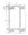
図1は、本発明の実施例によって製造された薄膜トランジスタ基板を示す平面図で、図2乃至図11は、図1に図示された薄膜トランジスタ基板の製造過程を示す工程図である。ここで、図2乃至図11は、図1のI−I’に沿って切断した場合の断面図である。 FIG. 1 is a plan view illustrating a thin film transistor substrate manufactured according to an embodiment of the present invention, and FIGS. 2 to 11 are process diagrams illustrating a manufacturing process of the thin film transistor substrate illustrated in FIG. 2 to 11 are cross-sectional views taken along the line I-I 'in FIG.
図1及び図2を参照すると、基板110上にゲート用金属膜を形成した後、第1露光マスクを利用したフォトリソグラフィ工程を通じて前記ゲート用金属膜をパターニングしてゲートライン122及びゲートライン122と連結されたゲート電極124を含むゲート配線120を形成する。前記ゲート用金属膜は、例えば、スパッタリング方法を通じて基板110上に形成されることができる。
Referring to FIGS. 1 and 2, after forming a gate metal film on the
基板110は、透明性絶縁基板、例えば、ガラス基板からなる。
The
ゲート配線120は、例えば、アルミニウム(Al)、モリブデン(Mo)、クロム(Cr)、タンタル(Ta)、チタニウム(Ti)、タングステン(W)、銅(Cu)、銀(Ag)等の単一金属又はこれらの合金で形成されることができる。又、ゲート配線120は、物理的性質の異なる2つ以上の金属層で形成されることができる。例えば、ゲート配線120は低抵抗配線のために、アルミニウム(Al)とモリブデン(Mo)が積層されたAl/Mo二層膜構造で形成されることができる。
The
ゲートライン122は、例えば、横方向に延長される。ゲート電極124はゲートライン122と連結され、各画素(P)に形成されるスイッチング素子である薄膜トランジスタTFTのゲート端子を構成する。
The
図3を参照すると、ゲート配線120が形成された基板110上にゲート絶縁膜130及び活性層140を順次に形成する。ゲート絶縁膜130及び活性層140は、例えば、プラズマ化学気相蒸着方法を通じて形成されることができる。
Referring to FIG. 3, the
ゲート絶縁膜130はゲート配線120を保護し、ゲート絶縁膜130の上部に形成されるデータ用金属膜150等と絶縁させるための絶縁膜であって、例えば、窒化シリコン(SiNx)又は酸化シリコン(SiOx)で形成され、CVD工程を通じて約4500Åの厚みに形成される。
The
活性層140は、チャンネル層142及びオーミックコンタクト層144を含む。例えば、チャンネル層142は、非晶質シリコン(以下、a−Si)で形成され、オーミックコンタクト層144は、n型不純物が高濃度でドーピングされた非晶質シリコン(以下、n+a−Si)で形成されることができる。
The
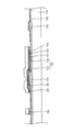
その後、活性層140上に第1金属層151、第2金属層152、及び第3金属層153を連続して積層してデータ用金属膜150を形成する。例えば、第1金属層151はモリブデン(Mo)、第2金属層152はアルミニウム(Al)、第3金属層153はモリブデン(Mo)で形成されることができる。従って、データ用金属膜150は、低抵抗配線の形成のために、Mo/Al/Mo三層膜構造で形成される。データ用金属膜150は、例えば、スパッタリング方法を通じて活性層140上に形成されることができる。
Thereafter, the
図4を参照すると、データ用金属膜150上にフォトレジストを形成した後、スリットマスク又はハーフトンマスク等の第2露光マスクを利用したフォトリソグラフィ工程を通じて前記フォトレジストをパターニングして第1フォトレジストパターン160を形成する。前記フォトレジストは、例えば、露光された領域が現像液によって除去されるポジティブ型フォトレジストで形成される。
Referring to FIG. 4, after a photoresist is formed on the
第1フォトレジストパターン160は、チャンネル形成領域に対応する部分が前記チャンネル形成領域以外に対応する部分に対して薄い厚みを有するように形成される。例えば、第1フォトレジストパターン160のチャンネル形成領域に対応する部分は、約5000〜8000Åの厚みに形成される。
The
図5を参照すると、第1フォトレジストパターン160をエッチングマスクとして利用して、データ用金属膜150のうち、最も上部に形成された第3金属層153をドライエッチングする。
Referring to FIG. 5, the
モリブデン(Mo)で形成された第3金属層153のドライエッチングのために、エッチングガスとしては六フッ化硫黄(SF6)ガスと塩素(Cl2)ガスが主に使用されることができる。例えば、六フッ化硫黄(SF6)ガスと塩素(Cl2)ガスは約1:0.5〜約1:1.5程度の組成比で混合され使用される。
For dry etching of the
図1及び図6を参照すると、第1フォトレジストパターン160をエッチングマスクとして利用して第2金属層152及び第1金属層151を同時にドライエッチングする。
Referring to FIGS. 1 and 6, the
アルミニウム(Al)で形成された第2金属層152とモリブデン(Mo)で形成された第1金属層151を同時にドライエッチングするために、エッチングガスとしては三塩化ホウ素(BCl3)ガスと塩素(Cl2)ガスが主に使用されることができる。例えば、三塩化ホウ素(BCl3)ガスと塩素(Cl2)ガスは約1:1〜約1:5程度の組成比で混合され使用される。アルミニウム(Al)で形成された第2金属層152のみをエッチングする場合に対して三塩化ホウ素(BCl3)の組成比率を高めることにより、第2金属層152と第1金属層151を同時にドライエッチングすることが可能になる。
In order to simultaneously dry-etch the
一方、第3金属層153、第2金属層152、及び第1金属層151をそれぞれドライエッチングする場合、チャンネル形成領域に位置するフォトレジストの残量不足によってドライエッチング途中に活性層140のチャンネル領域が開く現象が発生する。従って、第2金属層152と第1金属層151を同時にドライエッチングすることにより、工程を単純化させ、工程マージンを増加させてチャンネルが開く現象をある程度除去することができる。
On the other hand, when each of the
第1フォトレジストパターン160を利用したドライエッチング工程を通じて第3金属層153、第2金属層152、及び第1金属層151のエッチングが完了されると、データライン155とソース/ドレイン用金属パターン156のみが残ることになる。データライン155は、例えば、ゲートライン122と交差する縦方向に延長される。
When the etching of the
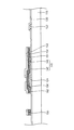
図7を参照すると、第1フォトレジストパターン160をエッチングマスクとして利用して活性層140をドライエッチングする。
Referring to FIG. 7, the
このように同じ第1フォトレジストパターン160を利用してデータ用金属膜150及び活性層140をエッチングすることにより、残られる活性層140の外部輪郭は、データライン155及びソース/ドレイン用金属パターン156の外部輪郭と実質的に一致するように形成される。
In this way, by etching the
図8を参照すると、酸素プラズマを利用したアッシング工程を通じて第1フォトレジストパターン160を一定厚みだけエッチングしてチャンネル形成領域に対応する部分が除去された第2フォトレジストパターン162を形成する。これによって、チャンネル形成領域に対応されるソース/ドレイン用金属パターン156が外部に露出される。
Referring to FIG. 8, the
図1及び図9を参照すると、第2フォトレジストパターン162をエッチングマスクとして利用してソース/ドレイン用金属パターン156のチャンネル形成領域をドライエッチングする。
Referring to FIGS. 1 and 9, the channel formation region of the source /
第2フォトレジストパターン162を利用したドライエッチング工程は、前述した第1フォトレジストパターン160を利用したドライエッチング工程と同様に、第3金属層153を1次にドライエッチングし、第2金属層152及び第1金属層151を同時に2次にドライエッチングする工程に進行されることができる。これと異なり、第2フォトレジストパターン162を利用したドライエッチング工程は、第3金属層153、第2金属層152、及び第1金属層151をそれぞれドライエッチングする工程に進行されることができる。
In the dry etching process using the
第2フォトレジストパターン162を利用したドライエッチング工程を通じてソース/ドレイン用金属パターン156のチャンネル形成領域のエッチングが完了されると、ソース電極157及びドレイン電極158が形成される。ソース電極157は、データライン155と連結され薄膜トランジスタTFTのソース端子を構成する。ドレイン電極158は、ソース電極157と離隔して薄膜トランジスタTFTのドレイン端子を構成する。
When the etching of the channel forming region of the source /
その後、第2フォトレジストパターン162をエッチングマスクとして利用してチャンネル形成領域のオーミックコンタクト層144をエッチングする。これによって、ソース電極157とドレイン電極158との間にはチャンネル層142が露出され薄膜トランジスタTFTのチャンネル159が形成される。
Thereafter, the
このように、第1、第2、及び第3金属層151、152、153で形成されたデータ用金属膜150の全てのエッチング工程をドライエッチング工程で進行することにより、ウェットエッチングによる配線幅増加等の問題点を改善し、製造工程をより単純化させることができる。
As described above, by performing all the etching processes of the
その後、データライン155、ソース電極157、及びドレイン電極158上に存在する第2フォトレジストパターン162を除去する。例えば、第2フォトレジストパターン162は、ストリップ溶液を利用したストリップ工程を通じて除去される。これによって、薄膜トランジスタTFTの製造が完了される。
Thereafter, the
図1及び図10を参照すると、薄膜トランジスタTFTが形成された基板110上に保護膜170を形成する。保護膜170は、薄膜トランジスタTFT及びデータライン155を保護して絶縁させるための絶縁膜であって、例えば、窒化シリコン(SiNx)又は酸化シリコン(SiOx)で形成され、CVD工程を通じて約500〜2000Åの厚みに形成される。
Referring to FIGS. 1 and 10, a
その後、第3露光マスクを利用したフォトリソグラフィ工程を通じて保護膜170をパターニングしてドレイン電極158の一部を露出させるコンタクトホール172を形成する。
Thereafter, the
図1及び図11を参照すると、保護膜170上に透明性導電膜を形成した後、第4露光マスクを利用したフォトリソグラフィ工程を通じて前記透明性導電膜をパターニングして各画素(P)内に画素電極180を形成する。
Referring to FIGS. 1 and 11, after forming a transparent conductive film on the
画素電極180は、保護膜170に形成されたコンタクトホール172を通じてドレイン電極158と電気的に連結される。画素電極180は、例えば、インジウムジンクオキサイド(IZO)又はインジウムティンオキサイド(ITO)で形成される。
The
一方、図示されていないが、画素電極180を形成する前に保護膜170上に平坦化のための有機絶縁膜を更に形成することができる。
On the other hand, although not shown, an organic insulating film for planarization can be further formed on the
図12乃至図15は、他の実施例によるデータ用金属膜のエッチング過程を示す工程図である。データ用金属膜を形成する過程までは、図2乃至図4に図示された工程図と同じなので、これらの図と関連する詳細な説明は省略する。 12 to 15 are process diagrams showing an etching process of a data metal film according to another embodiment. The process up to the formation of the data metal film is the same as the process charts shown in FIGS. 2 to 4, and a detailed description related to these figures will be omitted.
図12を参照すると、チャンネル形成領域に対応する部分が前記チャンネル形成領域以外に対応する部分に対して相対的に薄い厚みを有するフォトレジストパターン160をエッチングマスクとして利用して第3金属層153をドライエッチングする。
Referring to FIG. 12, the
モリブデン(Mo)で形成された第3金属層153のドライエッチングのために、エッチングガスとしてはフッ素(F)系列のガスと塩素(Cl2)ガスが使用される。例えば、フッ素(F)系列のガスとしては、六フッ化硫黄(SF6)ガスが使用されることができる。この際、六フッ化硫黄(SF6)ガスと塩素(Cl2)ガスは約1:0.5〜約1:1.5程度の組成比で混合され使用される。
For dry etching of the
図13を参照すると、フォトレジストパターン160をエッチングマスクとして利用して第2金属層152をドライエッチングする。
Referring to FIG. 13, the
アルミニウム(Al)で形成された第2金属層152のドライエッチングのために、エッチングガスとしては三塩化ホウ素(BCl3)ガスと塩素(Cl2)ガスが使用される。例えば、三塩化ホウ素(BCl3)ガスと塩素(Cl2)ガスは、第2金属層152のみをエッチングするために、約1:8〜約1:12程度の組成比で混合され使用される。
For dry etching of the
図14を参照すると、フォトレジストパターン160をエッチングマスクとして利用して第1金属層151と活性層140を同時にドライエッチングする。
Referring to FIG. 14, the
モリブデン(Mo)で形成された第1金属層151とa−Si及びn+a−Siで形成された活性層140を同時にドライエッチングするために、エッチングガスとしてはフッ素(F)系列のガスと塩素(Cl2)ガスが使用される。例えば、フッ素(F)系列のガスとしては六フッ化硫黄(SF6)ガスが使用されることができる。この際、六フッ化硫黄(SF6)ガスと塩素(Cl2)ガスは、約1:5〜約1:7程度の組成比で混合され使用される。このように、モリブデン(Mo)で形成された第1金属層151のみをエッチングする場合に対して塩素(Cl2)ガスの組成比率を高めることにより、第1金属層151と活性層140を同時にドライエッチングすることが可能になる。
In order to simultaneously dry-etch the
このように、第1金属層151と活性層140を同時にドライエッチングすることにより、工程を単純化させ、工程マージンを増加させてチャンネルが開く現象を完全に除去することができる。
As described above, the dry etching of the
一方、第1金属層151と活性層140を同時にドライエッチングする途中に、フォトレジストパターン160のチャンネル形成領域に対応する部分がオープンされ第3金属層153が同時にエッチングされる。
Meanwhile, during the dry etching of the
場合によっては、チャンネル形成領域にフォトレジストが残存することがあるので、チャンネル形成領域に残存するフォトレジストを完全に除去するために、アッシング工程を更に進行することができる。 In some cases, the photoresist may remain in the channel formation region, so that an ashing process can be further performed to completely remove the photoresist remaining in the channel formation region.
図15を参照すると、フォトレジストパターン160をエッチングマスクとして利用してチャンネル形成領域の第2金属層152及び第1金属層151をドライエッチングする。
Referring to FIG. 15, the
チャンネル形成領域の第2金属層152及び第1金属層151をドライエッチングする工程は、図9に説明したように、1回のドライエッチングで第2金属層152及び第1金属層151を同時にドライエッチングするか、第2金属層152及び第1金属層151をそれぞれドライエッチングする工程で進行されることができる。
In the step of dry etching the
以後、チャンネル形成領域のオーミックコンタクト層144をエッチングすると、ソース電極157とドレイン電極158との間のチャンネル層142が露出され薄膜トランジスタTFTのチャンネルが形成される。
Thereafter, when the
以後の製造工程は、図10及び図11に図示されたものと同じなので、これらの図と関連する詳細な説明は省略する。 Since the subsequent manufacturing steps are the same as those shown in FIGS. 10 and 11, detailed descriptions relating to these drawings are omitted.
このような薄膜トランジスタ基板の製造方法によると、低抵抗配線のために、Mo/Al/Mo三層膜構造で形成されたデータ用金属膜の全てのエッチング工程をドライエッチング工程で進行することにより、ウェットエッチングによって発生した配線幅増加等の問題点を改善し、製造工程を単純化させることができる。 According to such a method of manufacturing a thin film transistor substrate, for the low resistance wiring, by performing all the etching process of the data metal film formed of the Mo / Al / Mo three-layer film structure in the dry etching process, Problems such as an increase in wiring width caused by wet etching can be improved, and the manufacturing process can be simplified.
又、アルミニウムと下部モリブデンを同時にドライエッチングするか、下部モリブデンと活性層を同時にドライエッチングすることにより、製造工程をより単純化させ、工程マージンを増加させてチャンネルが開く現象を防止することができる。 Also, by simultaneously dry-etching aluminum and lower molybdenum or simultaneously dry-etching lower molybdenum and the active layer, the manufacturing process can be further simplified, and the process margin can be increased to prevent the channel from being opened. .
以上、本発明の実施例によって詳細に説明したが、本発明はこれに限定されず、本発明が属する技術分野において通常の知識を有するものであれば本発明の思想と精神を離れることなく、本発明を修正または変更できる。 As described above, the embodiments of the present invention have been described in detail. However, the present invention is not limited to the embodiments, and as long as it has ordinary knowledge in the technical field to which the present invention belongs, without departing from the spirit and spirit of the present invention, The present invention can be modified or changed.
本発明は、薄膜トランジスタ基板の製造方法に利用することができる。 The present invention can be used in a method for manufacturing a thin film transistor substrate.
110 基板、
122 ゲートライン、
124 ゲート電極、
130 ゲート絶縁層、
140 活性層、
142 チャンネル層、
144 オーミックコンタクト層、
150 データ用金属膜、
151 第1金属層、
152 第2金属層、
153 第3金属層、
155 データライン、
157 ソース電極、
158 ドレイン電極、
160 第1フォトレジストパターン、
162 第2フォトレジストパターン、
170 保護膜、
180 画素電極。
110 substrates,
122 gate line,
124 gate electrode,
130 gate insulating layer,
140 active layer,
142 channel layer,
144 ohmic contact layer,
150 Metal film for data,
151 the first metal layer,
152 second metal layer,
153 third metal layer,
155 data lines,
157 source electrode,
158 drain electrode,
160 a first photoresist pattern;
162 second photoresist pattern;
170 protective film,
180 pixel electrodes.
Claims (15)
前記活性層上に第1金属層、第2金属層、及び第3金属層が連続して積層されたデータ用金属膜を形成する段階と、
前記データ用金属膜上にチャンネル形成領域に対応する部分が前記チャンネル形成領域以外に対応する部分に対して相対的に薄い厚みを有する第1フォトレジストパターンを形成する段階と、
前記第1フォトレジストパターンを利用して前記第3金属層をドライエッチングする段階と、
前記第1フォトレジストパターンを利用して前記第2金属層及び前記第1金属層を同時にドライエッチングし、前記活性層が備えるオーミックコンタクト層を露出させ、データラインを形成する段階と、
前記第1フォトレジストパターンを利用して前記活性層をドライエッチングする段階と、
前記第1フォトレジストパターンをエッチングして前記チャンネル形成領域に対応する部分が除去された第2フォトレジストパターンを形成する段階と、
前記第2フォトレジストパターンを利用して前記データ用金属膜の前記チャンネル形成領域をドライエッチングして前記データラインと連結されたソース電極及び前記ソース電極と離隔したドレイン電極を形成する段階と、
を含むことを特徴とする薄膜トランジスタ基板の製造方法。 Sequentially forming a gate insulating film and an active layer on a substrate on which a gate line including a gate line and a gate electrode connected to the gate line is formed;
Forming a data metal layer in which a first metal layer, a second metal layer, and a third metal layer are sequentially stacked on the active layer;
Forming a first photoresist pattern in which a portion corresponding to a channel formation region has a relatively thin thickness on a portion of the data metal film corresponding to a portion other than the channel formation region;
Dry etching the third metal layer using the first photoresist pattern;
Using the first photoresist pattern to simultaneously dry-etch the second metal layer and the first metal layer, exposing an ohmic contact layer included in the active layer, and forming a data line;
Dry etching the active layer using the first photoresist pattern;
Etching the first photoresist pattern to form a second photoresist pattern in which a portion corresponding to the channel formation region is removed;
Using the second photoresist pattern to dry-etch the channel formation region of the data metal layer to form a source electrode connected to the data line and a drain electrode separated from the source electrode;
A method for manufacturing a thin film transistor substrate, comprising:
前記第2フォトレジストパターンを利用して前記第3金属層をドライエッチングする段階と、
前記第2フォトレジストパターンを利用して前記第2金属層及び前記第1金属層を同時にドライエッチングする段階と、
を含むことを特徴とする請求項1から4のいずれかに記載の薄膜トランジスタ基板の製造方法。 The step of dry etching the channel forming region of the data metal film using the second photoresist pattern comprises:
Dry etching the third metal layer using the second photoresist pattern;
Dry etching the second metal layer and the first metal layer simultaneously using the second photoresist pattern;
The method for producing a thin film transistor substrate according to claim 1, comprising:
前記ソース電極及びドレイン電極を形成する段階後に、前記第2フォトレジストパターンを利用して前記チャンネル形成領域の前記オーミックコンタクト層を除去して薄膜トランジスタを形成する段階を更に含むことを特徴とする請求項1から5のいずれかに記載の薄膜トランジスタ基板の製造方法。 The active layer includes a channel layer made of amorphous silicon and an ohmic contact layer made of amorphous silicon doped with ions,
The method further comprises forming a thin film transistor by removing the ohmic contact layer in the channel formation region using the second photoresist pattern after forming the source and drain electrodes. The manufacturing method of the thin-film transistor substrate in any one of 1-5.
前記保護膜上に前記ドレイン電極と電気的に連結される画素電極を形成する段階と、
を更に含むことを特徴とする請求項6記載の薄膜トランジスタ基板の製造方法。 Forming a protective film on the substrate on which the thin film transistor is formed;
Forming a pixel electrode electrically connected to the drain electrode on the protective layer;
The method of manufacturing a thin film transistor substrate according to claim 6, further comprising:
前記活性層上に第1金属層、第2金属層、及び第3金属層が連続して積層されたデータ用金属膜を形成する段階と、
前記データ用金属膜上にチャンネル形成領域に対応する部分が前記チャンネル形成領域以外に対応する部分に対して相対的に薄い厚みを有するフォトレジストパターンを形成する段階と、
前記フォトレジストパターンを利用して前記第3金属層をドライエッチングする段階と、
前記フォトレジストパターンを利用して前記第2金属層をドライエッチングする段階と、
前記フォトレジストパターンを利用して前記第1金属層及び前記活性層を同時にドライエッチングして、前記ゲート絶縁膜を露出させるとともに前記チャンネル形成領域に対応する部分をオープンしてデータラインを形成する段階と、
前記フォトレジストパターンを利用して前記データ用金属膜の前記チャンネル形成領域をドライエッチングして前記データラインと連結されたソース電極及び前記ソース電極と離隔したドレイン電極を形成する段階と、
を含む薄膜トランジスタ基板の製造方法。 Sequentially forming a gate insulating film and an active layer on a substrate on which a gate line including a gate line and a gate electrode connected to the gate line is formed;
Forming a data metal layer in which a first metal layer, a second metal layer, and a third metal layer are sequentially stacked on the active layer;
Forming a photoresist pattern in which a portion corresponding to a channel formation region has a relatively thin thickness on a portion corresponding to a region other than the channel formation region on the data metal film;
Dry etching the third metal layer using the photoresist pattern;
Dry etching the second metal layer using the photoresist pattern;
The photoresist pattern was simultaneously dry-etching the first metal layer and the active layer by using, to form the data lines to open a portion corresponding to the gate insulating film to expose the Rutotomoni the channel forming region Stages,
Using the photoresist pattern to dry-etch the channel formation region of the data metal film to form a source electrode connected to the data line and a drain electrode separated from the source electrode;
The manufacturing method of the thin-film transistor substrate containing this.
前記ソース電極及びドレイン電極を形成する段階後に、前記フォトレジストパターンを利用して前記チャンネル形成領域の前記オーミックコンタクト層を除去して薄膜トランジスタを形成する段階を更に含むことを特徴とする請求項8から13のいずれかに記載の薄膜トランジスタ基板の製造方法。 The active layer includes a channel layer made of amorphous silicon and an ohmic contact layer made of amorphous silicon doped with ions,
9. The method of claim 8, further comprising forming a thin film transistor by removing the ohmic contact layer in the channel formation region using the photoresist pattern after forming the source and drain electrodes. 14. A method for producing a thin film transistor substrate according to any one of 13 above.
前記保護膜上に前記ドレイン電極と電気的に連結される画素電極を形成する段階と、
を更に含むことを特徴とする請求項14記載の薄膜トランジスタ基板の製造方法。 Forming a protective film on the substrate on which the thin film transistor is formed;
Forming a pixel electrode electrically connected to the drain electrode on the protective layer;
The method of manufacturing a thin film transistor substrate according to claim 14, further comprising:
Applications Claiming Priority (2)
| Application Number | Priority Date | Filing Date | Title |
|---|---|---|---|
| KR1020060099187A KR101229277B1 (en) | 2006-10-12 | 2006-10-12 | Method of manufacturing thin film transistor substrate |
| KR10-2006-0099187 | 2006-10-12 |
Publications (3)
| Publication Number | Publication Date |
|---|---|
| JP2008098642A JP2008098642A (en) | 2008-04-24 |
| JP2008098642A5 JP2008098642A5 (en) | 2011-10-27 |
| JP5679397B2 true JP5679397B2 (en) | 2015-03-04 |
Family
ID=38941886
Family Applications (1)
| Application Number | Title | Priority Date | Filing Date |
|---|---|---|---|
| JP2007265748A Active JP5679397B2 (en) | 2006-10-12 | 2007-10-11 | Method for manufacturing thin film transistor substrate |
Country Status (6)
| Country | Link |
|---|---|
| US (1) | US7803673B2 (en) |
| EP (1) | EP1912256A1 (en) |
| JP (1) | JP5679397B2 (en) |
| KR (1) | KR101229277B1 (en) |
| CN (1) | CN101162710A (en) |
| TW (1) | TWI423394B (en) |
Families Citing this family (6)
| Publication number | Priority date | Publication date | Assignee | Title |
|---|---|---|---|---|
| KR20070038610A (en) * | 2005-10-06 | 2007-04-11 | 삼성전자주식회사 | Repair apparatus and repair method of indicators |
| US8791001B2 (en) * | 2008-09-08 | 2014-07-29 | Taiwan Semiconductor Manufacturing Company, Ltd. | N2 based plasma treatment and ash for HK metal gate protection |
| KR101042957B1 (en) * | 2010-03-19 | 2011-06-20 | 삼성모바일디스플레이주식회사 | Transistor substrate, and manufacturing method thereof |
| US8163620B2 (en) * | 2010-04-21 | 2012-04-24 | Institute of Microelectronics, Chinese Academy of Sciences | Method for etching Mo-based metal gate stack with aluminium nitride barrier |
| US8329518B1 (en) * | 2011-08-11 | 2012-12-11 | Shenzhen China Star Optoelectronics Technology Co., Ltd. | Methods for manufacturing thin film transistor array substrate and display panel |
| KR102245497B1 (en) * | 2014-08-08 | 2021-04-29 | 삼성디스플레이 주식회사 | Display substrate and method of manufacturing the same |
Family Cites Families (11)
| Publication number | Priority date | Publication date | Assignee | Title |
|---|---|---|---|---|
| US6472329B1 (en) * | 1999-08-16 | 2002-10-29 | Applied Komatsu Technology, Inc. | Etching aluminum over refractory metal with successive plasmas |
| JP4683688B2 (en) | 2000-03-16 | 2011-05-18 | 株式会社半導体エネルギー研究所 | Method for manufacturing liquid crystal display device |
| TW490857B (en) | 2001-02-05 | 2002-06-11 | Samsung Electronics Co Ltd | Thin film transistor array substrate for liquid crystal display and method of fabricating same |
| JP4603190B2 (en) | 2001-04-16 | 2010-12-22 | 株式会社日立製作所 | Liquid crystal display |
| JP4920140B2 (en) * | 2001-05-18 | 2012-04-18 | ゲットナー・ファンデーション・エルエルシー | Liquid crystal display device and manufacturing method thereof |
| JP4050503B2 (en) * | 2001-11-29 | 2008-02-20 | 株式会社日立製作所 | Display device |
| JP4221314B2 (en) * | 2004-02-10 | 2009-02-12 | Nec液晶テクノロジー株式会社 | THIN FILM TRANSISTOR, LIQUID CRYSTAL DISPLAY DEVICE USING THE SAME, AND METHOD FOR PRODUCING THE THIN FILM TRANSISTOR |
| KR101136026B1 (en) * | 2004-09-24 | 2012-04-18 | 주식회사 동진쎄미켐 | Composition for stripping photoresist and method for manufacturing thin film transistor array panel using the same |
| KR101090252B1 (en) * | 2004-09-24 | 2011-12-06 | 삼성전자주식회사 | Thin film transistor array panel and manufacturing method thereof |
| KR20060081470A (en) * | 2005-01-07 | 2006-07-13 | 삼성전자주식회사 | Thin film transistor substrate and its manufacturing method |
| KR20060089526A (en) * | 2005-02-04 | 2006-08-09 | 삼성전자주식회사 | Thin film transistor array panel and manufacturing method thereof |
-
2006
- 2006-10-12 KR KR1020060099187A patent/KR101229277B1/en active Active
-
2007
- 2007-10-11 EP EP07019889A patent/EP1912256A1/en not_active Ceased
- 2007-10-11 JP JP2007265748A patent/JP5679397B2/en active Active
- 2007-10-12 US US11/871,457 patent/US7803673B2/en active Active
- 2007-10-12 CN CNA2007101524343A patent/CN101162710A/en active Pending
- 2007-10-12 TW TW096138226A patent/TWI423394B/en active
Also Published As
| Publication number | Publication date |
|---|---|
| US7803673B2 (en) | 2010-09-28 |
| KR20080033590A (en) | 2008-04-17 |
| CN101162710A (en) | 2008-04-16 |
| KR101229277B1 (en) | 2013-02-04 |
| TWI423394B (en) | 2014-01-11 |
| TW200828505A (en) | 2008-07-01 |
| EP1912256A1 (en) | 2008-04-16 |
| JP2008098642A (en) | 2008-04-24 |
| US20080090342A1 (en) | 2008-04-17 |
Similar Documents
| Publication | Publication Date | Title |
|---|---|---|
| US8563980B2 (en) | Array substrate and manufacturing method | |
| US6207480B1 (en) | Method of manufacturing a thin film transistor array panel for a liquid crystal display | |
| KR100917654B1 (en) | TFT-LCD pixel unit and method for manufacturing the same | |
| KR101431136B1 (en) | Method of manufacturing thin film transistor substrate | |
| JP4994014B2 (en) | Method for manufacturing thin film transistor used in flat panel display | |
| US7649581B2 (en) | Array substrate of an LCD comprising first and second gate insulating layers and method of fabricating the same | |
| KR20080012810A (en) | Thin-film transistor LCD pixel unit and manufacturing method thereof | |
| JP2008109102A (en) | Method for manufacturing thin film transistor substrate | |
| JP2004226975A (en) | Thin film transistor panel and method of manufacturing the same | |
| JP5679397B2 (en) | Method for manufacturing thin film transistor substrate | |
| KR20040086946A (en) | Manufacturing method of the liquid crystal display device | |
| CN108803168B (en) | Array substrate, manufacturing method thereof and liquid crystal display device | |
| TWI424507B (en) | Method for manufacturing thin film transistor array substrate | |
| KR101432109B1 (en) | Manufacturing method of thin film transistor | |
| JP4578402B2 (en) | Thin film transistor substrate and manufacturing method thereof | |
| KR101813719B1 (en) | Manufacturing method of thin film transisotr array substrate | |
| US20170110490A1 (en) | Mask and method for manufacturing thin film transistor using the same | |
| KR102035004B1 (en) | Array substrate for liquid crystal display device and method of fabricating the same | |
| US20080188042A1 (en) | Method of manufacturing thin film transistor panel | |
| CN102830531B (en) | TFT (Thin Film Transistor) array substrate, manufacturing method and liquid crystal display device | |
| KR100848110B1 (en) | Thin film transistor substrate for liquid crystal display device and manufacturing method thereof | |
| KR100930573B1 (en) | Thin film transistor manufacturing method and display device manufacturing method using same | |
| JPH04357832A (en) | Etching method and manufacture of thin film transistor | |
| KR20080022829A (en) | Method of manufacturing thin film transistor substrate | |
| KR20080051483A (en) | Method of manufacturing thin film transistor substrate |
Legal Events
| Date | Code | Title | Description |
|---|---|---|---|
| A621 | Written request for application examination |
Free format text: JAPANESE INTERMEDIATE CODE: A621 Effective date: 20101008 |
|
| A521 | Request for written amendment filed |
Free format text: JAPANESE INTERMEDIATE CODE: A523 Effective date: 20101015 |
|
| A521 | Request for written amendment filed |
Free format text: JAPANESE INTERMEDIATE CODE: A523 Effective date: 20110909 |
|
| A711 | Notification of change in applicant |
Free format text: JAPANESE INTERMEDIATE CODE: A712 Effective date: 20121213 |
|
| A977 | Report on retrieval |
Free format text: JAPANESE INTERMEDIATE CODE: A971007 Effective date: 20130228 |
|
| A131 | Notification of reasons for refusal |
Free format text: JAPANESE INTERMEDIATE CODE: A131 Effective date: 20130305 |
|
| A521 | Request for written amendment filed |
Free format text: JAPANESE INTERMEDIATE CODE: A523 Effective date: 20130520 |
|
| A02 | Decision of refusal |
Free format text: JAPANESE INTERMEDIATE CODE: A02 Effective date: 20131008 |
|
| A521 | Request for written amendment filed |
Free format text: JAPANESE INTERMEDIATE CODE: A523 Effective date: 20140128 |
|
| A911 | Transfer to examiner for re-examination before appeal (zenchi) |
Free format text: JAPANESE INTERMEDIATE CODE: A911 Effective date: 20140204 |
|
| A912 | Re-examination (zenchi) completed and case transferred to appeal board |
Free format text: JAPANESE INTERMEDIATE CODE: A912 Effective date: 20140314 |
|
| A61 | First payment of annual fees (during grant procedure) |
Free format text: JAPANESE INTERMEDIATE CODE: A61 Effective date: 20141226 |
|
| R150 | Certificate of patent or registration of utility model |
Ref document number: 5679397 Country of ref document: JP Free format text: JAPANESE INTERMEDIATE CODE: R150 |
|
| R250 | Receipt of annual fees |
Free format text: JAPANESE INTERMEDIATE CODE: R250 |
|
| R250 | Receipt of annual fees |
Free format text: JAPANESE INTERMEDIATE CODE: R250 |
|
| R250 | Receipt of annual fees |
Free format text: JAPANESE INTERMEDIATE CODE: R250 |
|
| R250 | Receipt of annual fees |
Free format text: JAPANESE INTERMEDIATE CODE: R250 |
|
| R250 | Receipt of annual fees |
Free format text: JAPANESE INTERMEDIATE CODE: R250 |
|
| S111 | Request for change of ownership or part of ownership |
Free format text: JAPANESE INTERMEDIATE CODE: R313113 |
|
| R360 | Written notification for declining of transfer of rights |
Free format text: JAPANESE INTERMEDIATE CODE: R360 |
|
| R360 | Written notification for declining of transfer of rights |
Free format text: JAPANESE INTERMEDIATE CODE: R360 |
|
| R371 | Transfer withdrawn |
Free format text: JAPANESE INTERMEDIATE CODE: R371 |
|
| S111 | Request for change of ownership or part of ownership |
Free format text: JAPANESE INTERMEDIATE CODE: R313113 |
|
| R350 | Written notification of registration of transfer |
Free format text: JAPANESE INTERMEDIATE CODE: R350 |
|
| R250 | Receipt of annual fees |
Free format text: JAPANESE INTERMEDIATE CODE: R250 |
|
| R250 | Receipt of annual fees |
Free format text: JAPANESE INTERMEDIATE CODE: R250 |
|
| R250 | Receipt of annual fees |
Free format text: JAPANESE INTERMEDIATE CODE: R250 |
|
| R250 | Receipt of annual fees |
Free format text: JAPANESE INTERMEDIATE CODE: R250 |