JP5656330B2 - Method for manufacturing photoelectric conversion device - Google Patents
Method for manufacturing photoelectric conversion device Download PDFInfo
- Publication number
- JP5656330B2 JP5656330B2 JP2011132818A JP2011132818A JP5656330B2 JP 5656330 B2 JP5656330 B2 JP 5656330B2 JP 2011132818 A JP2011132818 A JP 2011132818A JP 2011132818 A JP2011132818 A JP 2011132818A JP 5656330 B2 JP5656330 B2 JP 5656330B2
- Authority
- JP
- Japan
- Prior art keywords
- semiconductor region
- crystalline semiconductor
- conductivity type
- photoelectric conversion
- intrinsic
- Prior art date
- Legal status (The legal status is an assumption and is not a legal conclusion. Google has not performed a legal analysis and makes no representation as to the accuracy of the status listed.)
- Expired - Fee Related
Links
- 238000006243 chemical reaction Methods 0.000 title claims description 106
- 238000000034 method Methods 0.000 title claims description 50
- 238000004519 manufacturing process Methods 0.000 title claims description 11
- 239000004065 semiconductor Substances 0.000 claims description 457
- 229910052710 silicon Inorganic materials 0.000 claims description 54
- 239000010703 silicon Substances 0.000 claims description 54
- 239000012535 impurity Substances 0.000 claims description 52
- 238000004518 low pressure chemical vapour deposition Methods 0.000 claims description 42
- 238000000151 deposition Methods 0.000 claims description 28
- 230000008021 deposition Effects 0.000 claims description 25
- 239000010410 layer Substances 0.000 description 156
- XUIMIQQOPSSXEZ-UHFFFAOYSA-N Silicon Chemical compound [Si] XUIMIQQOPSSXEZ-UHFFFAOYSA-N 0.000 description 48
- 239000007789 gas Substances 0.000 description 42
- 239000000758 substrate Substances 0.000 description 34
- 239000000463 material Substances 0.000 description 20
- 229910052751 metal Inorganic materials 0.000 description 19
- 239000002184 metal Substances 0.000 description 18
- 229910021332 silicide Inorganic materials 0.000 description 16
- FVBUAEGBCNSCDD-UHFFFAOYSA-N silicide(4-) Chemical compound [Si-4] FVBUAEGBCNSCDD-UHFFFAOYSA-N 0.000 description 16
- XLOMVQKBTHCTTD-UHFFFAOYSA-N Zinc monoxide Chemical compound [Zn]=O XLOMVQKBTHCTTD-UHFFFAOYSA-N 0.000 description 11
- RTAQQCXQSZGOHL-UHFFFAOYSA-N Titanium Chemical compound [Ti] RTAQQCXQSZGOHL-UHFFFAOYSA-N 0.000 description 10
- 239000013078 crystal Substances 0.000 description 9
- XYFCBTPGUUZFHI-UHFFFAOYSA-N Phosphine Chemical compound P XYFCBTPGUUZFHI-UHFFFAOYSA-N 0.000 description 8
- 239000004020 conductor Substances 0.000 description 8
- 229910021420 polycrystalline silicon Inorganic materials 0.000 description 8
- ZOXJGFHDIHLPTG-UHFFFAOYSA-N Boron Chemical compound [B] ZOXJGFHDIHLPTG-UHFFFAOYSA-N 0.000 description 7
- 229910052796 boron Inorganic materials 0.000 description 7
- 238000005530 etching Methods 0.000 description 7
- 239000007788 liquid Substances 0.000 description 7
- BASFCYQUMIYNBI-UHFFFAOYSA-N platinum Chemical compound [Pt] BASFCYQUMIYNBI-UHFFFAOYSA-N 0.000 description 7
- 239000012670 alkaline solution Substances 0.000 description 6
- 229910052782 aluminium Inorganic materials 0.000 description 6
- XAGFODPZIPBFFR-UHFFFAOYSA-N aluminium Chemical compound [Al] XAGFODPZIPBFFR-UHFFFAOYSA-N 0.000 description 6
- 229910021417 amorphous silicon Inorganic materials 0.000 description 6
- 238000000576 coating method Methods 0.000 description 6
- 229910021419 crystalline silicon Inorganic materials 0.000 description 6
- 230000007547 defect Effects 0.000 description 6
- 238000010438 heat treatment Methods 0.000 description 6
- 229920005591 polysilicon Polymers 0.000 description 6
- UFHFLCQGNIYNRP-UHFFFAOYSA-N Hydrogen Chemical compound [H][H] UFHFLCQGNIYNRP-UHFFFAOYSA-N 0.000 description 5
- PXHVJJICTQNCMI-UHFFFAOYSA-N Nickel Chemical compound [Ni] PXHVJJICTQNCMI-UHFFFAOYSA-N 0.000 description 5
- KDLHZDBZIXYQEI-UHFFFAOYSA-N Palladium Chemical compound [Pd] KDLHZDBZIXYQEI-UHFFFAOYSA-N 0.000 description 5
- 239000010949 copper Substances 0.000 description 5
- 230000000694 effects Effects 0.000 description 5
- 229910052739 hydrogen Inorganic materials 0.000 description 5
- 239000001257 hydrogen Substances 0.000 description 5
- 238000005268 plasma chemical vapour deposition Methods 0.000 description 5
- 239000011787 zinc oxide Substances 0.000 description 5
- IJGRMHOSHXDMSA-UHFFFAOYSA-N Atomic nitrogen Chemical compound N#N IJGRMHOSHXDMSA-UHFFFAOYSA-N 0.000 description 4
- RYGMFSIKBFXOCR-UHFFFAOYSA-N Copper Chemical compound [Cu] RYGMFSIKBFXOCR-UHFFFAOYSA-N 0.000 description 4
- 229910052802 copper Inorganic materials 0.000 description 4
- 239000010419 fine particle Substances 0.000 description 4
- 229910000073 phosphorus hydride Inorganic materials 0.000 description 4
- ZOKXTWBITQBERF-UHFFFAOYSA-N Molybdenum Chemical compound [Mo] ZOKXTWBITQBERF-UHFFFAOYSA-N 0.000 description 3
- BLRPTPMANUNPDV-UHFFFAOYSA-N Silane Chemical compound [SiH4] BLRPTPMANUNPDV-UHFFFAOYSA-N 0.000 description 3
- HEMHJVSKTPXQMS-UHFFFAOYSA-M Sodium hydroxide Chemical compound [OH-].[Na+] HEMHJVSKTPXQMS-UHFFFAOYSA-M 0.000 description 3
- 229910052785 arsenic Inorganic materials 0.000 description 3
- RQNWIZPPADIBDY-UHFFFAOYSA-N arsenic atom Chemical compound [As] RQNWIZPPADIBDY-UHFFFAOYSA-N 0.000 description 3
- 238000005229 chemical vapour deposition Methods 0.000 description 3
- 239000011651 chromium Substances 0.000 description 3
- 229910017052 cobalt Inorganic materials 0.000 description 3
- 239000010941 cobalt Substances 0.000 description 3
- GUTLYIVDDKVIGB-UHFFFAOYSA-N cobalt atom Chemical compound [Co] GUTLYIVDDKVIGB-UHFFFAOYSA-N 0.000 description 3
- 230000003247 decreasing effect Effects 0.000 description 3
- 238000001704 evaporation Methods 0.000 description 3
- 239000010408 film Substances 0.000 description 3
- 239000011888 foil Substances 0.000 description 3
- AMGQUBHHOARCQH-UHFFFAOYSA-N indium;oxotin Chemical compound [In].[Sn]=O AMGQUBHHOARCQH-UHFFFAOYSA-N 0.000 description 3
- 229910052750 molybdenum Inorganic materials 0.000 description 3
- 239000011733 molybdenum Substances 0.000 description 3
- 229910052697 platinum Inorganic materials 0.000 description 3
- 238000007639 printing Methods 0.000 description 3
- 238000004544 sputter deposition Methods 0.000 description 3
- XOLBLPGZBRYERU-UHFFFAOYSA-N tin dioxide Chemical compound O=[Sn]=O XOLBLPGZBRYERU-UHFFFAOYSA-N 0.000 description 3
- 229910001887 tin oxide Inorganic materials 0.000 description 3
- 229910052719 titanium Inorganic materials 0.000 description 3
- 239000010936 titanium Substances 0.000 description 3
- XKRFYHLGVUSROY-UHFFFAOYSA-N Argon Chemical compound [Ar] XKRFYHLGVUSROY-UHFFFAOYSA-N 0.000 description 2
- CURLTUGMZLYLDI-UHFFFAOYSA-N Carbon dioxide Chemical compound O=C=O CURLTUGMZLYLDI-UHFFFAOYSA-N 0.000 description 2
- VYZAMTAEIAYCRO-UHFFFAOYSA-N Chromium Chemical compound [Cr] VYZAMTAEIAYCRO-UHFFFAOYSA-N 0.000 description 2
- KRHYYFGTRYWZRS-UHFFFAOYSA-N Fluorane Chemical compound F KRHYYFGTRYWZRS-UHFFFAOYSA-N 0.000 description 2
- OAICVXFJPJFONN-UHFFFAOYSA-N Phosphorus Chemical compound [P] OAICVXFJPJFONN-UHFFFAOYSA-N 0.000 description 2
- 229920001609 Poly(3,4-ethylenedioxythiophene) Polymers 0.000 description 2
- 229910052581 Si3N4 Inorganic materials 0.000 description 2
- BQCADISMDOOEFD-UHFFFAOYSA-N Silver Chemical compound [Ag] BQCADISMDOOEFD-UHFFFAOYSA-N 0.000 description 2
- RBFQJDQYXXHULB-UHFFFAOYSA-N arsane Chemical compound [AsH3] RBFQJDQYXXHULB-UHFFFAOYSA-N 0.000 description 2
- 229910052804 chromium Inorganic materials 0.000 description 2
- 238000011109 contamination Methods 0.000 description 2
- 239000002612 dispersion medium Substances 0.000 description 2
- 239000011521 glass Substances 0.000 description 2
- 239000010931 gold Substances 0.000 description 2
- 238000005984 hydrogenation reaction Methods 0.000 description 2
- 229910044991 metal oxide Inorganic materials 0.000 description 2
- 150000004706 metal oxides Chemical class 0.000 description 2
- 229910021421 monocrystalline silicon Inorganic materials 0.000 description 2
- 229910052759 nickel Inorganic materials 0.000 description 2
- 229910052758 niobium Inorganic materials 0.000 description 2
- 239000010955 niobium Substances 0.000 description 2
- GUCVJGMIXFAOAE-UHFFFAOYSA-N niobium atom Chemical compound [Nb] GUCVJGMIXFAOAE-UHFFFAOYSA-N 0.000 description 2
- 229910052757 nitrogen Inorganic materials 0.000 description 2
- 229910052763 palladium Inorganic materials 0.000 description 2
- 239000011574 phosphorus Substances 0.000 description 2
- 229910052698 phosphorus Inorganic materials 0.000 description 2
- 229920000172 poly(styrenesulfonic acid) Polymers 0.000 description 2
- 229940005642 polystyrene sulfonic acid Drugs 0.000 description 2
- 238000010248 power generation Methods 0.000 description 2
- 238000007789 sealing Methods 0.000 description 2
- 229910052990 silicon hydride Inorganic materials 0.000 description 2
- HQVNEWCFYHHQES-UHFFFAOYSA-N silicon nitride Chemical compound N12[Si]34N5[Si]62N3[Si]51N64 HQVNEWCFYHHQES-UHFFFAOYSA-N 0.000 description 2
- FDNAPBUWERUEDA-UHFFFAOYSA-N silicon tetrachloride Chemical compound Cl[Si](Cl)(Cl)Cl FDNAPBUWERUEDA-UHFFFAOYSA-N 0.000 description 2
- ABTOQLMXBSRXSM-UHFFFAOYSA-N silicon tetrafluoride Chemical compound F[Si](F)(F)F ABTOQLMXBSRXSM-UHFFFAOYSA-N 0.000 description 2
- 229910052709 silver Inorganic materials 0.000 description 2
- 239000004332 silver Substances 0.000 description 2
- 239000000243 solution Substances 0.000 description 2
- 239000002904 solvent Substances 0.000 description 2
- 239000000126 substance Substances 0.000 description 2
- 229910052715 tantalum Inorganic materials 0.000 description 2
- GUVRBAGPIYLISA-UHFFFAOYSA-N tantalum atom Chemical compound [Ta] GUVRBAGPIYLISA-UHFFFAOYSA-N 0.000 description 2
- 239000010409 thin film Substances 0.000 description 2
- 229910052720 vanadium Inorganic materials 0.000 description 2
- GPPXJZIENCGNKB-UHFFFAOYSA-N vanadium Chemical compound [V]#[V] GPPXJZIENCGNKB-UHFFFAOYSA-N 0.000 description 2
- XLYOFNOQVPJJNP-UHFFFAOYSA-N water Substances O XLYOFNOQVPJJNP-UHFFFAOYSA-N 0.000 description 2
- WEAMLHXSIBDPGN-UHFFFAOYSA-N (4-hydroxy-3-methylphenyl) thiocyanate Chemical compound CC1=CC(SC#N)=CC=C1O WEAMLHXSIBDPGN-UHFFFAOYSA-N 0.000 description 1
- PFNQVRZLDWYSCW-UHFFFAOYSA-N (fluoren-9-ylideneamino) n-naphthalen-1-ylcarbamate Chemical compound C12=CC=CC=C2C2=CC=CC=C2C1=NOC(=O)NC1=CC=CC2=CC=CC=C12 PFNQVRZLDWYSCW-UHFFFAOYSA-N 0.000 description 1
- 229910000838 Al alloy Inorganic materials 0.000 description 1
- JBRZTFJDHDCESZ-UHFFFAOYSA-N AsGa Chemical compound [As]#[Ga] JBRZTFJDHDCESZ-UHFFFAOYSA-N 0.000 description 1
- 229910002601 GaN Inorganic materials 0.000 description 1
- 229910001218 Gallium arsenide Inorganic materials 0.000 description 1
- JMASRVWKEDWRBT-UHFFFAOYSA-N Gallium nitride Chemical compound [Ga]#N JMASRVWKEDWRBT-UHFFFAOYSA-N 0.000 description 1
- GPXJNWSHGFTCBW-UHFFFAOYSA-N Indium phosphide Chemical compound [In]#P GPXJNWSHGFTCBW-UHFFFAOYSA-N 0.000 description 1
- XEEYBQQBJWHFJM-UHFFFAOYSA-N Iron Chemical compound [Fe] XEEYBQQBJWHFJM-UHFFFAOYSA-N 0.000 description 1
- 229910052779 Neodymium Inorganic materials 0.000 description 1
- 229910003902 SiCl 4 Inorganic materials 0.000 description 1
- 229910000577 Silicon-germanium Inorganic materials 0.000 description 1
- 229910006404 SnO 2 Inorganic materials 0.000 description 1
- QCWXUUIWCKQGHC-UHFFFAOYSA-N Zirconium Chemical compound [Zr] QCWXUUIWCKQGHC-UHFFFAOYSA-N 0.000 description 1
- LEVVHYCKPQWKOP-UHFFFAOYSA-N [Si].[Ge] Chemical compound [Si].[Ge] LEVVHYCKPQWKOP-UHFFFAOYSA-N 0.000 description 1
- TWRSDLOICOIGRH-UHFFFAOYSA-N [Si].[Si].[Hf] Chemical compound [Si].[Si].[Hf] TWRSDLOICOIGRH-UHFFFAOYSA-N 0.000 description 1
- 150000001298 alcohols Chemical class 0.000 description 1
- 229910045601 alloy Inorganic materials 0.000 description 1
- 239000000956 alloy Substances 0.000 description 1
- 239000005407 aluminoborosilicate glass Substances 0.000 description 1
- 239000005354 aluminosilicate glass Substances 0.000 description 1
- 229910052786 argon Inorganic materials 0.000 description 1
- 229910052788 barium Inorganic materials 0.000 description 1
- DSAJWYNOEDNPEQ-UHFFFAOYSA-N barium atom Chemical compound [Ba] DSAJWYNOEDNPEQ-UHFFFAOYSA-N 0.000 description 1
- 230000015572 biosynthetic process Effects 0.000 description 1
- YXTPWUNVHCYOSP-UHFFFAOYSA-N bis($l^{2}-silanylidene)molybdenum Chemical compound [Si]=[Mo]=[Si] YXTPWUNVHCYOSP-UHFFFAOYSA-N 0.000 description 1
- 239000005388 borosilicate glass Substances 0.000 description 1
- 239000001569 carbon dioxide Substances 0.000 description 1
- 229910002092 carbon dioxide Inorganic materials 0.000 description 1
- 239000000969 carrier Substances 0.000 description 1
- 238000003486 chemical etching Methods 0.000 description 1
- 229910021357 chromium silicide Inorganic materials 0.000 description 1
- 238000004140 cleaning Methods 0.000 description 1
- 239000011248 coating agent Substances 0.000 description 1
- 229920001940 conductive polymer Polymers 0.000 description 1
- 238000003618 dip coating Methods 0.000 description 1
- 238000001035 drying Methods 0.000 description 1
- 230000005611 electricity Effects 0.000 description 1
- 238000007772 electroless plating Methods 0.000 description 1
- 239000003792 electrolyte Substances 0.000 description 1
- 238000009713 electroplating Methods 0.000 description 1
- 238000005516 engineering process Methods 0.000 description 1
- 150000002170 ethers Chemical class 0.000 description 1
- 229910052732 germanium Inorganic materials 0.000 description 1
- GNPVGFCGXDBREM-UHFFFAOYSA-N germanium atom Chemical compound [Ge] GNPVGFCGXDBREM-UHFFFAOYSA-N 0.000 description 1
- PCHJSUWPFVWCPO-UHFFFAOYSA-N gold Chemical compound [Au] PCHJSUWPFVWCPO-UHFFFAOYSA-N 0.000 description 1
- 229910052737 gold Inorganic materials 0.000 description 1
- 229910052735 hafnium Inorganic materials 0.000 description 1
- VBJZVLUMGGDVMO-UHFFFAOYSA-N hafnium atom Chemical compound [Hf] VBJZVLUMGGDVMO-UHFFFAOYSA-N 0.000 description 1
- 239000001307 helium Substances 0.000 description 1
- 229910052734 helium Inorganic materials 0.000 description 1
- SWQJXJOGLNCZEY-UHFFFAOYSA-N helium atom Chemical compound [He] SWQJXJOGLNCZEY-UHFFFAOYSA-N 0.000 description 1
- 150000002430 hydrocarbons Chemical class 0.000 description 1
- 238000009413 insulation Methods 0.000 description 1
- 238000005468 ion implantation Methods 0.000 description 1
- 239000011344 liquid material Substances 0.000 description 1
- ORUIBWPALBXDOA-UHFFFAOYSA-L magnesium fluoride Chemical compound [F-].[F-].[Mg+2] ORUIBWPALBXDOA-UHFFFAOYSA-L 0.000 description 1
- 229910001635 magnesium fluoride Inorganic materials 0.000 description 1
- 150000002739 metals Chemical class 0.000 description 1
- 238000002156 mixing Methods 0.000 description 1
- 229910021344 molybdenum silicide Inorganic materials 0.000 description 1
- QEFYFXOXNSNQGX-UHFFFAOYSA-N neodymium atom Chemical compound [Nd] QEFYFXOXNSNQGX-UHFFFAOYSA-N 0.000 description 1
- 229910052754 neon Inorganic materials 0.000 description 1
- GKAOGPIIYCISHV-UHFFFAOYSA-N neon atom Chemical compound [Ne] GKAOGPIIYCISHV-UHFFFAOYSA-N 0.000 description 1
- RUFLMLWJRZAWLJ-UHFFFAOYSA-N nickel silicide Chemical compound [Ni]=[Si]=[Ni] RUFLMLWJRZAWLJ-UHFFFAOYSA-N 0.000 description 1
- 229910021334 nickel silicide Inorganic materials 0.000 description 1
- 239000011368 organic material Substances 0.000 description 1
- 230000000737 periodic effect Effects 0.000 description 1
- 229920000767 polyaniline Polymers 0.000 description 1
- 229920000128 polypyrrole Polymers 0.000 description 1
- 229920000123 polythiophene Polymers 0.000 description 1
- 239000011241 protective layer Substances 0.000 description 1
- 239000010453 quartz Substances 0.000 description 1
- 230000006798 recombination Effects 0.000 description 1
- 238000005215 recombination Methods 0.000 description 1
- 230000002441 reversible effect Effects 0.000 description 1
- 238000005070 sampling Methods 0.000 description 1
- 229910052594 sapphire Inorganic materials 0.000 description 1
- 239000010980 sapphire Substances 0.000 description 1
- 229910052706 scandium Inorganic materials 0.000 description 1
- SIXSYDAISGFNSX-UHFFFAOYSA-N scandium atom Chemical compound [Sc] SIXSYDAISGFNSX-UHFFFAOYSA-N 0.000 description 1
- 239000003566 sealing material Substances 0.000 description 1
- 229910000077 silane Inorganic materials 0.000 description 1
- HBMJWWWQQXIZIP-UHFFFAOYSA-N silicon carbide Chemical compound [Si+]#[C-] HBMJWWWQQXIZIP-UHFFFAOYSA-N 0.000 description 1
- 229910010271 silicon carbide Inorganic materials 0.000 description 1
- VYPSYNLAJGMNEJ-UHFFFAOYSA-N silicon dioxide Inorganic materials O=[Si]=O VYPSYNLAJGMNEJ-UHFFFAOYSA-N 0.000 description 1
- 238000003980 solgel method Methods 0.000 description 1
- 238000004528 spin coating Methods 0.000 description 1
- 238000005507 spraying Methods 0.000 description 1
- 239000010935 stainless steel Substances 0.000 description 1
- 229910001220 stainless steel Inorganic materials 0.000 description 1
- 229910021341 titanium silicide Inorganic materials 0.000 description 1
- WFKWXMTUELFFGS-UHFFFAOYSA-N tungsten Chemical compound [W] WFKWXMTUELFFGS-UHFFFAOYSA-N 0.000 description 1
- 229910052721 tungsten Inorganic materials 0.000 description 1
- 239000010937 tungsten Substances 0.000 description 1
- -1 tungsten (W) Chemical class 0.000 description 1
- 238000007740 vapor deposition Methods 0.000 description 1
- 239000012808 vapor phase Substances 0.000 description 1
- 238000001947 vapour-phase growth Methods 0.000 description 1
- 238000010792 warming Methods 0.000 description 1
- 229910052724 xenon Inorganic materials 0.000 description 1
- FHNFHKCVQCLJFQ-UHFFFAOYSA-N xenon atom Chemical compound [Xe] FHNFHKCVQCLJFQ-UHFFFAOYSA-N 0.000 description 1
- 229910052726 zirconium Inorganic materials 0.000 description 1
- 229910021355 zirconium silicide Inorganic materials 0.000 description 1
Images


Classifications
-
- H—ELECTRICITY
- H01—ELECTRIC ELEMENTS
- H01L—SEMICONDUCTOR DEVICES NOT COVERED BY CLASS H10
- H01L31/00—Semiconductor devices sensitive to infrared radiation, light, electromagnetic radiation of shorter wavelength or corpuscular radiation and specially adapted either for the conversion of the energy of such radiation into electrical energy or for the control of electrical energy by such radiation; Processes or apparatus specially adapted for the manufacture or treatment thereof or of parts thereof; Details thereof
- H01L31/02—Details
- H01L31/0236—Special surface textures
-
- H—ELECTRICITY
- H01—ELECTRIC ELEMENTS
- H01L—SEMICONDUCTOR DEVICES NOT COVERED BY CLASS H10
- H01L31/00—Semiconductor devices sensitive to infrared radiation, light, electromagnetic radiation of shorter wavelength or corpuscular radiation and specially adapted either for the conversion of the energy of such radiation into electrical energy or for the control of electrical energy by such radiation; Processes or apparatus specially adapted for the manufacture or treatment thereof or of parts thereof; Details thereof
- H01L31/0248—Semiconductor devices sensitive to infrared radiation, light, electromagnetic radiation of shorter wavelength or corpuscular radiation and specially adapted either for the conversion of the energy of such radiation into electrical energy or for the control of electrical energy by such radiation; Processes or apparatus specially adapted for the manufacture or treatment thereof or of parts thereof; Details thereof characterised by their semiconductor bodies
- H01L31/0256—Semiconductor devices sensitive to infrared radiation, light, electromagnetic radiation of shorter wavelength or corpuscular radiation and specially adapted either for the conversion of the energy of such radiation into electrical energy or for the control of electrical energy by such radiation; Processes or apparatus specially adapted for the manufacture or treatment thereof or of parts thereof; Details thereof characterised by their semiconductor bodies characterised by the material
- H01L31/0264—Inorganic materials
- H01L31/028—Inorganic materials including, apart from doping material or other impurities, only elements of Group IV of the Periodic Table
-
- H—ELECTRICITY
- H01—ELECTRIC ELEMENTS
- H01L—SEMICONDUCTOR DEVICES NOT COVERED BY CLASS H10
- H01L31/00—Semiconductor devices sensitive to infrared radiation, light, electromagnetic radiation of shorter wavelength or corpuscular radiation and specially adapted either for the conversion of the energy of such radiation into electrical energy or for the control of electrical energy by such radiation; Processes or apparatus specially adapted for the manufacture or treatment thereof or of parts thereof; Details thereof
- H01L31/0248—Semiconductor devices sensitive to infrared radiation, light, electromagnetic radiation of shorter wavelength or corpuscular radiation and specially adapted either for the conversion of the energy of such radiation into electrical energy or for the control of electrical energy by such radiation; Processes or apparatus specially adapted for the manufacture or treatment thereof or of parts thereof; Details thereof characterised by their semiconductor bodies
- H01L31/0352—Semiconductor devices sensitive to infrared radiation, light, electromagnetic radiation of shorter wavelength or corpuscular radiation and specially adapted either for the conversion of the energy of such radiation into electrical energy or for the control of electrical energy by such radiation; Processes or apparatus specially adapted for the manufacture or treatment thereof or of parts thereof; Details thereof characterised by their semiconductor bodies characterised by their shape or by the shapes, relative sizes or disposition of the semiconductor regions
- H01L31/035272—Semiconductor devices sensitive to infrared radiation, light, electromagnetic radiation of shorter wavelength or corpuscular radiation and specially adapted either for the conversion of the energy of such radiation into electrical energy or for the control of electrical energy by such radiation; Processes or apparatus specially adapted for the manufacture or treatment thereof or of parts thereof; Details thereof characterised by their semiconductor bodies characterised by their shape or by the shapes, relative sizes or disposition of the semiconductor regions characterised by at least one potential jump barrier or surface barrier
- H01L31/035281—Shape of the body
-
- H—ELECTRICITY
- H01—ELECTRIC ELEMENTS
- H01L—SEMICONDUCTOR DEVICES NOT COVERED BY CLASS H10
- H01L31/00—Semiconductor devices sensitive to infrared radiation, light, electromagnetic radiation of shorter wavelength or corpuscular radiation and specially adapted either for the conversion of the energy of such radiation into electrical energy or for the control of electrical energy by such radiation; Processes or apparatus specially adapted for the manufacture or treatment thereof or of parts thereof; Details thereof
- H01L31/0248—Semiconductor devices sensitive to infrared radiation, light, electromagnetic radiation of shorter wavelength or corpuscular radiation and specially adapted either for the conversion of the energy of such radiation into electrical energy or for the control of electrical energy by such radiation; Processes or apparatus specially adapted for the manufacture or treatment thereof or of parts thereof; Details thereof characterised by their semiconductor bodies
- H01L31/0352—Semiconductor devices sensitive to infrared radiation, light, electromagnetic radiation of shorter wavelength or corpuscular radiation and specially adapted either for the conversion of the energy of such radiation into electrical energy or for the control of electrical energy by such radiation; Processes or apparatus specially adapted for the manufacture or treatment thereof or of parts thereof; Details thereof characterised by their semiconductor bodies characterised by their shape or by the shapes, relative sizes or disposition of the semiconductor regions
- H01L31/035272—Semiconductor devices sensitive to infrared radiation, light, electromagnetic radiation of shorter wavelength or corpuscular radiation and specially adapted either for the conversion of the energy of such radiation into electrical energy or for the control of electrical energy by such radiation; Processes or apparatus specially adapted for the manufacture or treatment thereof or of parts thereof; Details thereof characterised by their semiconductor bodies characterised by their shape or by the shapes, relative sizes or disposition of the semiconductor regions characterised by at least one potential jump barrier or surface barrier
- H01L31/03529—Shape of the potential jump barrier or surface barrier
-
- H—ELECTRICITY
- H01—ELECTRIC ELEMENTS
- H01L—SEMICONDUCTOR DEVICES NOT COVERED BY CLASS H10
- H01L31/00—Semiconductor devices sensitive to infrared radiation, light, electromagnetic radiation of shorter wavelength or corpuscular radiation and specially adapted either for the conversion of the energy of such radiation into electrical energy or for the control of electrical energy by such radiation; Processes or apparatus specially adapted for the manufacture or treatment thereof or of parts thereof; Details thereof
- H01L31/0248—Semiconductor devices sensitive to infrared radiation, light, electromagnetic radiation of shorter wavelength or corpuscular radiation and specially adapted either for the conversion of the energy of such radiation into electrical energy or for the control of electrical energy by such radiation; Processes or apparatus specially adapted for the manufacture or treatment thereof or of parts thereof; Details thereof characterised by their semiconductor bodies
- H01L31/036—Semiconductor devices sensitive to infrared radiation, light, electromagnetic radiation of shorter wavelength or corpuscular radiation and specially adapted either for the conversion of the energy of such radiation into electrical energy or for the control of electrical energy by such radiation; Processes or apparatus specially adapted for the manufacture or treatment thereof or of parts thereof; Details thereof characterised by their semiconductor bodies characterised by their crystalline structure or particular orientation of the crystalline planes
- H01L31/0392—Semiconductor devices sensitive to infrared radiation, light, electromagnetic radiation of shorter wavelength or corpuscular radiation and specially adapted either for the conversion of the energy of such radiation into electrical energy or for the control of electrical energy by such radiation; Processes or apparatus specially adapted for the manufacture or treatment thereof or of parts thereof; Details thereof characterised by their semiconductor bodies characterised by their crystalline structure or particular orientation of the crystalline planes including thin films deposited on metallic or insulating substrates ; characterised by specific substrate materials or substrate features or by the presence of intermediate layers, e.g. barrier layers, on the substrate
- H01L31/03921—Semiconductor devices sensitive to infrared radiation, light, electromagnetic radiation of shorter wavelength or corpuscular radiation and specially adapted either for the conversion of the energy of such radiation into electrical energy or for the control of electrical energy by such radiation; Processes or apparatus specially adapted for the manufacture or treatment thereof or of parts thereof; Details thereof characterised by their semiconductor bodies characterised by their crystalline structure or particular orientation of the crystalline planes including thin films deposited on metallic or insulating substrates ; characterised by specific substrate materials or substrate features or by the presence of intermediate layers, e.g. barrier layers, on the substrate including only elements of Group IV of the Periodic Table
-
- H—ELECTRICITY
- H01—ELECTRIC ELEMENTS
- H01L—SEMICONDUCTOR DEVICES NOT COVERED BY CLASS H10
- H01L31/00—Semiconductor devices sensitive to infrared radiation, light, electromagnetic radiation of shorter wavelength or corpuscular radiation and specially adapted either for the conversion of the energy of such radiation into electrical energy or for the control of electrical energy by such radiation; Processes or apparatus specially adapted for the manufacture or treatment thereof or of parts thereof; Details thereof
- H01L31/04—Semiconductor devices sensitive to infrared radiation, light, electromagnetic radiation of shorter wavelength or corpuscular radiation and specially adapted either for the conversion of the energy of such radiation into electrical energy or for the control of electrical energy by such radiation; Processes or apparatus specially adapted for the manufacture or treatment thereof or of parts thereof; Details thereof adapted as photovoltaic [PV] conversion devices
- H01L31/06—Semiconductor devices sensitive to infrared radiation, light, electromagnetic radiation of shorter wavelength or corpuscular radiation and specially adapted either for the conversion of the energy of such radiation into electrical energy or for the control of electrical energy by such radiation; Processes or apparatus specially adapted for the manufacture or treatment thereof or of parts thereof; Details thereof adapted as photovoltaic [PV] conversion devices characterised by potential barriers
- H01L31/072—Semiconductor devices sensitive to infrared radiation, light, electromagnetic radiation of shorter wavelength or corpuscular radiation and specially adapted either for the conversion of the energy of such radiation into electrical energy or for the control of electrical energy by such radiation; Processes or apparatus specially adapted for the manufacture or treatment thereof or of parts thereof; Details thereof adapted as photovoltaic [PV] conversion devices characterised by potential barriers the potential barriers being only of the PN heterojunction type
-
- H—ELECTRICITY
- H01—ELECTRIC ELEMENTS
- H01L—SEMICONDUCTOR DEVICES NOT COVERED BY CLASS H10
- H01L31/00—Semiconductor devices sensitive to infrared radiation, light, electromagnetic radiation of shorter wavelength or corpuscular radiation and specially adapted either for the conversion of the energy of such radiation into electrical energy or for the control of electrical energy by such radiation; Processes or apparatus specially adapted for the manufacture or treatment thereof or of parts thereof; Details thereof
- H01L31/04—Semiconductor devices sensitive to infrared radiation, light, electromagnetic radiation of shorter wavelength or corpuscular radiation and specially adapted either for the conversion of the energy of such radiation into electrical energy or for the control of electrical energy by such radiation; Processes or apparatus specially adapted for the manufacture or treatment thereof or of parts thereof; Details thereof adapted as photovoltaic [PV] conversion devices
- H01L31/06—Semiconductor devices sensitive to infrared radiation, light, electromagnetic radiation of shorter wavelength or corpuscular radiation and specially adapted either for the conversion of the energy of such radiation into electrical energy or for the control of electrical energy by such radiation; Processes or apparatus specially adapted for the manufacture or treatment thereof or of parts thereof; Details thereof adapted as photovoltaic [PV] conversion devices characterised by potential barriers
- H01L31/075—Semiconductor devices sensitive to infrared radiation, light, electromagnetic radiation of shorter wavelength or corpuscular radiation and specially adapted either for the conversion of the energy of such radiation into electrical energy or for the control of electrical energy by such radiation; Processes or apparatus specially adapted for the manufacture or treatment thereof or of parts thereof; Details thereof adapted as photovoltaic [PV] conversion devices characterised by potential barriers the potential barriers being only of the PIN type, e.g. amorphous silicon PIN solar cells
-
- H—ELECTRICITY
- H01—ELECTRIC ELEMENTS
- H01L—SEMICONDUCTOR DEVICES NOT COVERED BY CLASS H10
- H01L31/00—Semiconductor devices sensitive to infrared radiation, light, electromagnetic radiation of shorter wavelength or corpuscular radiation and specially adapted either for the conversion of the energy of such radiation into electrical energy or for the control of electrical energy by such radiation; Processes or apparatus specially adapted for the manufacture or treatment thereof or of parts thereof; Details thereof
- H01L31/18—Processes or apparatus specially adapted for the manufacture or treatment of these devices or of parts thereof
- H01L31/1804—Processes or apparatus specially adapted for the manufacture or treatment of these devices or of parts thereof comprising only elements of Group IV of the Periodic Table
-
- Y—GENERAL TAGGING OF NEW TECHNOLOGICAL DEVELOPMENTS; GENERAL TAGGING OF CROSS-SECTIONAL TECHNOLOGIES SPANNING OVER SEVERAL SECTIONS OF THE IPC; TECHNICAL SUBJECTS COVERED BY FORMER USPC CROSS-REFERENCE ART COLLECTIONS [XRACs] AND DIGESTS
- Y02—TECHNOLOGIES OR APPLICATIONS FOR MITIGATION OR ADAPTATION AGAINST CLIMATE CHANGE
- Y02E—REDUCTION OF GREENHOUSE GAS [GHG] EMISSIONS, RELATED TO ENERGY GENERATION, TRANSMISSION OR DISTRIBUTION
- Y02E10/00—Energy generation through renewable energy sources
- Y02E10/50—Photovoltaic [PV] energy
- Y02E10/547—Monocrystalline silicon PV cells
-
- Y—GENERAL TAGGING OF NEW TECHNOLOGICAL DEVELOPMENTS; GENERAL TAGGING OF CROSS-SECTIONAL TECHNOLOGIES SPANNING OVER SEVERAL SECTIONS OF THE IPC; TECHNICAL SUBJECTS COVERED BY FORMER USPC CROSS-REFERENCE ART COLLECTIONS [XRACs] AND DIGESTS
- Y02—TECHNOLOGIES OR APPLICATIONS FOR MITIGATION OR ADAPTATION AGAINST CLIMATE CHANGE
- Y02E—REDUCTION OF GREENHOUSE GAS [GHG] EMISSIONS, RELATED TO ENERGY GENERATION, TRANSMISSION OR DISTRIBUTION
- Y02E10/00—Energy generation through renewable energy sources
- Y02E10/50—Photovoltaic [PV] energy
- Y02E10/548—Amorphous silicon PV cells
-
- Y—GENERAL TAGGING OF NEW TECHNOLOGICAL DEVELOPMENTS; GENERAL TAGGING OF CROSS-SECTIONAL TECHNOLOGIES SPANNING OVER SEVERAL SECTIONS OF THE IPC; TECHNICAL SUBJECTS COVERED BY FORMER USPC CROSS-REFERENCE ART COLLECTIONS [XRACs] AND DIGESTS
- Y02—TECHNOLOGIES OR APPLICATIONS FOR MITIGATION OR ADAPTATION AGAINST CLIMATE CHANGE
- Y02P—CLIMATE CHANGE MITIGATION TECHNOLOGIES IN THE PRODUCTION OR PROCESSING OF GOODS
- Y02P70/00—Climate change mitigation technologies in the production process for final industrial or consumer products
- Y02P70/50—Manufacturing or production processes characterised by the final manufactured product
Landscapes
- Engineering & Computer Science (AREA)
- Microelectronics & Electronic Packaging (AREA)
- Electromagnetism (AREA)
- General Physics & Mathematics (AREA)
- Condensed Matter Physics & Semiconductors (AREA)
- Computer Hardware Design (AREA)
- Physics & Mathematics (AREA)
- Power Engineering (AREA)
- Chemical & Material Sciences (AREA)
- Manufacturing & Machinery (AREA)
- Inorganic Chemistry (AREA)
- Crystallography & Structural Chemistry (AREA)
- Photovoltaic Devices (AREA)
Description
本発明は、光電変換装置及びその作製方法に関する。 The present invention relates to a photoelectric conversion device and a manufacturing method thereof.
近年、地球温暖化対策として、発電時に二酸化炭素の排出の無い発電手段である光電変換装置が注目されている。その代表例としては、屋外において太陽光で発電する住宅用等の電力供給用太陽電池が知られている。この様な太陽電池には、主に単結晶シリコンや多結晶シリコンなどの結晶性シリコン太陽電池が用いられている。 In recent years, photoelectric conversion devices, which are power generation means that do not emit carbon dioxide during power generation, have attracted attention as a measure against global warming. As a typical example, a solar cell for power supply such as a house for generating electricity with sunlight outdoors is known. For such solar cells, crystalline silicon solar cells such as single crystal silicon and polycrystalline silicon are mainly used.
単結晶シリコン基板や多結晶シリコン基板を用いた太陽電池の表面は、表面反射を低減するために凹凸構造(テクスチャー構造ともいう)が形成されている。シリコン基板の表面に形成される凹凸構造は、シリコン基板を水酸化ナトリウム水溶液などのアルカリ溶液でエッチングして形成される。アルカリ溶液は、シリコンの結晶面方位に対してエッチング速度が異なるため、例えば(100)面のシリコン基板を用いれば、ピラミッド型の凹凸構造が形成される。 An uneven structure (also referred to as a texture structure) is formed on the surface of a solar cell using a single crystal silicon substrate or a polycrystalline silicon substrate in order to reduce surface reflection. The uneven structure formed on the surface of the silicon substrate is formed by etching the silicon substrate with an alkaline solution such as an aqueous sodium hydroxide solution. Since the etching speed of the alkaline solution differs with respect to the crystal plane orientation of silicon, for example, if a (100) plane silicon substrate is used, a pyramidal concavo-convex structure is formed.
上記のような凹凸構造は太陽電池の表面反射を低減することができるが、エッチングのために用いるアルカリ溶液はシリコン半導体の汚染源にもなるので適切でない。また、アルカリ溶液の濃度や温度によってエッチング特性が大幅に異なるので、シリコン基板の表面に凹凸構造を再現性良く作り込むのには困難が伴う。そのために、レーザ加工技術と化学エッチングを組み合わせた方法が開示されている(例えば、特許文献1参照)。 Although the concavo-convex structure as described above can reduce the surface reflection of the solar cell, the alkaline solution used for etching is not appropriate because it also becomes a contamination source of the silicon semiconductor. In addition, since the etching characteristics vary greatly depending on the concentration and temperature of the alkaline solution, it is difficult to create a concavo-convex structure on the surface of the silicon substrate with good reproducibility. Therefore, a method combining laser processing technology and chemical etching is disclosed (for example, see Patent Document 1).
一方、シリコンなどの半導体の薄膜を光電変換層とする太陽電池では、上記のようなアルカリ溶液を用いたエッチングでシリコン薄膜の表面に凹凸構造を作り込むことは困難である。 On the other hand, in a solar cell using a semiconductor thin film such as silicon as a photoelectric conversion layer, it is difficult to form an uneven structure on the surface of the silicon thin film by etching using an alkaline solution as described above.
いずれにしても、シリコン基板の表面に凹凸構造を形成するために、シリコン基板自体をエッチングする方法は、凹凸形状の制御性に問題があり、太陽電池の特性にも影響を与えるので好ましくない。また、シリコン基板のエッチングのためにアルカリ溶液や、多量の洗浄水が必要となり、シリコン基板の汚染にも注意を払う必要があるため、生産性の観点からも好ましくない。 In any case, the method of etching the silicon substrate itself in order to form a concavo-convex structure on the surface of the silicon substrate is not preferable because it has a problem in controllability of the concavo-convex shape and affects the characteristics of the solar cell. In addition, an alkaline solution or a large amount of cleaning water is required for etching the silicon substrate, and it is necessary to pay attention to contamination of the silicon substrate, which is not preferable from the viewpoint of productivity.
そこで、本発明の一形態は、新しい反射防止構造を有する光電変換装置を提供することを課題とする。 An object of one embodiment of the present invention is to provide a photoelectric conversion device having a new antireflection structure.
本発明の一形態は、半導体表面に同種または異種の半導体の結晶を成長させて凹凸構造とし、反射防止構造を形成することを要旨とする。これによって、半導体基板または半導体膜の表面をエッチングする必要がなくなる。 One aspect of the present invention is to form an uneven structure by growing a semiconductor crystal of the same kind or different kind on a semiconductor surface to form an antireflection structure. This eliminates the need to etch the surface of the semiconductor substrate or semiconductor film.
例えば、光電変換装置の光入射面側に、表面に複数の突起部を有する半導体層を設けることで、表面反射を大幅に低減する。かかる構造は、気相成長法で作製することができるので、半導体を汚染することがない。 For example, surface reflection is significantly reduced by providing a semiconductor layer having a plurality of protrusions on the surface on the light incident surface side of the photoelectric conversion device. Since such a structure can be manufactured by a vapor deposition method, the semiconductor is not contaminated.
気相成長法によれば、凹凸構造としてウィスカーを複数有する半導体層を成長させることが可能であり、これによって光電変換装置の反射防止構造とすることができる。 According to the vapor phase growth method, a semiconductor layer having a plurality of whiskers can be grown as a concavo-convex structure, whereby an antireflection structure of a photoelectric conversion device can be obtained.
また、本発明の一形態は、導電層上に設けられた第1の導電型である結晶性半導体領域と、第1の導電型である結晶性半導体領域上に設けられ、結晶性半導体で形成された複数のウィスカーを有することにより凹凸表面を有し、第1の導電型を付与する不純物元素の濃度勾配を有する結晶性半導体領域と、凹凸表面を有する結晶性半導体領域の該凹凸表面を被覆するように設けられた第1の導電型とは逆の第2の導電型である結晶性半導体領域と、を有する光電変換装置である。 Another embodiment of the present invention is a crystalline semiconductor region which is a first conductivity type provided over a conductive layer and a crystalline semiconductor region which is provided over a crystalline semiconductor region which is a first conductivity type and is formed using a crystalline semiconductor A crystalline semiconductor region having a concavo-convex surface by having a plurality of whiskers and having a concentration gradient of an impurity element imparting the first conductivity type, and covering the concavo-convex surface of the crystalline semiconductor region having the concavo-convex surface And a crystalline semiconductor region having a second conductivity type opposite to the first conductivity type.
また、本発明の一形態は、電極上に積層された第1の導電型である結晶性半導体領域、真性である結晶性半導体領域、及び第2の導電型である半導体領域を有し、電極及び第1の導電型である結晶性半導体領域の界面が平坦であり、真性である結晶性半導体領域が、結晶性半導体領域、及び当該結晶性半導体領域上に設けられ、結晶性半導体で形成される複数のウィスカーを有することを特徴とする光電変換装置である。即ち、真性である結晶性半導体領域は、複数のウィスカーを有するため、第2の導電型である半導体領域の表面が凹凸状である。更に、真性である半導体領域及び第2の導電型である半導体領域の界面は凹凸状である。そして、第1の導電型である結晶性半導体領域から真性である結晶性半導体領域の方向に、第1の導電型を付与する不純物元素の濃度勾配を有している。 Another embodiment of the present invention includes a crystalline semiconductor region that is a first conductivity type, an intrinsic crystalline semiconductor region, and a semiconductor region that is a second conductivity type, which are stacked over the electrode, And the crystalline semiconductor region having the first conductivity type is flat, and the intrinsic crystalline semiconductor region is provided on the crystalline semiconductor region and the crystalline semiconductor region, and is formed of the crystalline semiconductor. A photoelectric conversion device having a plurality of whiskers. In other words, since the intrinsic crystalline semiconductor region has a plurality of whiskers, the surface of the semiconductor region of the second conductivity type is uneven. Further, the interface between the intrinsic semiconductor region and the second conductivity type semiconductor region is uneven. Then, a concentration gradient of the impurity element imparting the first conductivity type is provided in the direction from the crystalline semiconductor region having the first conductivity type to the intrinsic crystalline semiconductor region.
本発明の一形態は、電極上に積層された第1の導電型である結晶性半導体領域、真性である結晶性半導体領域、及び第2の導電型である半導体領域を有し、電極及び第1の導電型である結晶性半導体領域の界面が平坦であり、第1の導電型である結晶性半導体領域が、第1の導電型を付与する不純物元素を有する結晶性半導体領域、及び当該結晶性半導体領域上に設けられ、第1の導電型を付与する不純物元素を有する結晶性半導体で形成される複数のウィスカーを有することを特徴とする光電変換装置である。即ち、第1の導電型である結晶性半導体領域は、複数のウィスカーを有するため、第2の導電型である半導体領域の表面が凹凸状である。更に、第1の導電型である結晶性半導体領域及び真性である結晶性半導体領域の界面は凹凸状である。そして、第1の導電型である結晶性半導体領域から真性である結晶性半導体領域の方向に、第1の導電型を付与する不純物元素の濃度勾配を有している。 One embodiment of the present invention includes a crystalline semiconductor region that is a first conductivity type, an intrinsic crystalline semiconductor region, and a semiconductor region that is a second conductivity type, which are stacked over an electrode. A crystalline semiconductor region in which the interface of the crystalline semiconductor region of one conductivity type is flat, the crystalline semiconductor region of the first conductivity type includes an impurity element imparting the first conductivity type, and the crystal A photoelectric conversion device including a plurality of whiskers that are formed over a crystalline semiconductor region and are formed using a crystalline semiconductor including an impurity element imparting a first conductivity type. That is, since the crystalline semiconductor region having the first conductivity type has a plurality of whiskers, the surface of the semiconductor region having the second conductivity type is uneven. Furthermore, the interface between the crystalline semiconductor region which is the first conductivity type and the intrinsic crystalline semiconductor region is uneven. Then, a concentration gradient of the impurity element imparting the first conductivity type is provided in the direction from the crystalline semiconductor region having the first conductivity type to the intrinsic crystalline semiconductor region.
なお、上記光電変換装置において、第1の導電型である結晶性半導体領域は、n型半導体領域及びp型半導体領域の一方であり、第2の導電型である半導体領域は、n型半導体領域及びp型半導体領域の他方である。 Note that in the above photoelectric conversion device, the crystalline semiconductor region having the first conductivity type is one of the n-type semiconductor region and the p-type semiconductor region, and the semiconductor region having the second conductivity type is the n-type semiconductor region. And the other of the p-type semiconductor regions.
上記光電変換装置において、第2の導電型である半導体領域は、非晶質半導体または結晶性半導体を用いることができる。または、非晶質半導体と結晶性半導体とが混在した半導体材料を用いることができる。 In the photoelectric conversion device, an amorphous semiconductor or a crystalline semiconductor can be used for the semiconductor region of the second conductivity type. Alternatively, a semiconductor material in which an amorphous semiconductor and a crystalline semiconductor are mixed can be used.
上記光電変換装置において、真性である結晶性半導体領域及び第2の導電型である半導体領域は、バンドギャップが異なる材料を用いてもよい。上記光電変換装置において、第2の導電型である半導体領域は、真性である結晶性半導体領域よりバンドギャップの大きい材料を用いてもよい。 In the above photoelectric conversion device, materials having different band gaps may be used for the intrinsic crystalline semiconductor region and the second conductivity type semiconductor region. In the photoelectric conversion device, a material having a larger band gap than the intrinsic crystalline semiconductor region may be used for the semiconductor region having the second conductivity type.
また、本発明の一形態は、上記第2の導電型である半導体領域上に積層された第3の導電型である半導体領域、真性である半導体領域、及び第4の導電型である半導体領域を有する光電変換装置である。なお、真性である結晶性半導体領域と真性である半導体領域とは、バンドギャップが異なる。 Another embodiment of the present invention is a semiconductor region which is a third conductivity type, an intrinsic semiconductor region, and a semiconductor region which is a fourth conductivity type, which are stacked over the semiconductor region which is the second conductivity type. The photoelectric conversion device having Note that a band gap is different between an intrinsic crystalline semiconductor region and an intrinsic semiconductor region.
なお、上記光電変換装置において、第1の導電型である結晶性半導体領域及び第3の導電型である半導体領域は、n型半導体領域及びp型半導体領域の一方であり、第2の導電型である半導体領域及び第4の導電型である半導体領域は、n型半導体領域及びp型半導体領域の他方である。 Note that in the photoelectric conversion device, the crystalline semiconductor region which is the first conductivity type and the semiconductor region which is the third conductivity type are one of the n-type semiconductor region and the p-type semiconductor region, and the second conductivity type. The semiconductor region that is and the semiconductor region that is the fourth conductivity type are the other of the n-type semiconductor region and the p-type semiconductor region.
第1の導電型である結晶性半導体領域若しくは真性である結晶性半導体領域に形成される複数のウィスカーの軸の方向は、電極の法線方向であってもよい。または、第1の導電型である結晶性半導体領域若しくは真性である結晶性半導体領域に形成される複数のウィスカーの軸の方向は、不揃いであってもよい。 The direction of the axes of the plurality of whiskers formed in the crystalline semiconductor region that is the first conductivity type or the intrinsic crystalline semiconductor region may be the normal direction of the electrode. Alternatively, the directions of the axes of the plurality of whiskers formed in the crystalline semiconductor region that is the first conductivity type or the intrinsic crystalline semiconductor region may be uneven.
電極は、少なくとも導電層又は混合層の一方を有する。電極は、導電層及び混合層を有する場合もある。また、電極の全部が混合層である場合もある。また、混合層がない場合もある。導電層は、シリコンと反応してシリサイドを形成する金属元素で形成することができる。または、導電層は、白金、アルミニウム、銅に代表される金属元素等の導電性の高い材料で形成される層と、シリコンと反応してシリサイドを形成する金属元素で形成される層との積層構造とすることができる。 The electrode has at least one of a conductive layer or a mixed layer. The electrode may have a conductive layer and a mixed layer. In some cases, the entire electrode is a mixed layer. Also, there may be no mixed layer. The conductive layer can be formed using a metal element that forms silicide by reacting with silicon. Alternatively, the conductive layer is a stack of a layer formed using a highly conductive material such as a metal element typified by platinum, aluminum, or copper and a layer formed using a metal element that forms silicide by reacting with silicon. It can be a structure.
混合層は、金属元素及びシリコンを有する。混合層としては、導電層を形成する金属元素及びシリコンを有してもよい。また、導電層をシリコンと反応してシリサイドを形成する金属元素で形成する場合、混合層は、シリサイドで形成されてもよい。 The mixed layer includes a metal element and silicon. As the mixed layer, a metal element forming a conductive layer and silicon may be included. When the conductive layer is formed using a metal element that forms silicide by reacting with silicon, the mixed layer may be formed using silicide.
光電変換装置において、第1の導電型である結晶性半導体領域または真性である結晶性半導体領域に複数のウィスカーを有することで、第2の導電型である半導体領域の表面における光の反射率を低減することができる。さらに、光電変換層に入射した光は、光閉じ込め効果により光電変換層で吸収されるため、光電変換装置の特性を高めることができる。 In the photoelectric conversion device, by including a plurality of whiskers in the crystalline semiconductor region that is the first conductivity type or the crystalline semiconductor region that is intrinsic, the reflectance of light on the surface of the semiconductor region that is the second conductivity type is increased. Can be reduced. Furthermore, since the light incident on the photoelectric conversion layer is absorbed by the photoelectric conversion layer due to the light confinement effect, the characteristics of the photoelectric conversion device can be improved.
また、本発明の一形態は、導電層上に、シリコンを含む堆積性ガス及び第1の導電型を付与するガスを原料ガスに用い550℃より高く650℃より低い温度で低圧化学的気相堆積法(以下、減圧CVD法またはLPCVD:(Low Pressure Chemical Vapor Deposition)法とも示す。)により、第1の導電型である結晶性半導体領域を形成し、シリコンを含む堆積性ガスを原料ガスに用い550℃より高く650℃より低い温度で減圧CVD法により、第1の導電型である結晶性半導体領域上に、結晶性半導体領域及び結晶性半導体で形成される複数のウィスカーを有する真性である結晶性半導体領域を形成するとともに、第1の導電型である結晶性半導体領域から真性である結晶性半導体領域の方向に、第1の導電型を付与する不純物元素を移動させ、シリコンを含む堆積性ガス及び第2の導電型を付与するガスを原料ガスに用い550℃以下または650℃以上の温度で減圧CVD法により、真性である結晶性半導体領域上に第2の導電型である半導体領域を形成することを特徴とする光電変換装置の作製方法である。第1の導電型である結晶性半導体領域を形成する際に、上記導電層及び第1の導電型である結晶性半導体領域の間に混合層が形成される場合もある。 Another embodiment of the present invention is a low-pressure chemical vapor phase at a temperature higher than 550 ° C. and lower than 650 ° C. using a deposition gas containing silicon and a gas imparting the first conductivity type as a source gas over a conductive layer. A crystalline semiconductor region which is a first conductivity type is formed by a deposition method (hereinafter also referred to as a low pressure CVD method or LPCVD: (Low Pressure Chemical Vapor Deposition) method), and a deposition gas containing silicon is used as a source gas. Use intrinsically having a crystalline semiconductor region and a plurality of whiskers formed of the crystalline semiconductor on the crystalline semiconductor region of the first conductivity type by a low pressure CVD method at a temperature higher than 550 ° C. and lower than 650 ° C. The crystalline semiconductor region is formed from the crystalline semiconductor region of the first conductivity type to the intrinsic crystalline semiconductor region. In addition, the impurity element imparting the first conductivity type is moved, the deposition gas containing silicon and the gas imparting the second conductivity type are used as the source gas, and the low pressure CVD method at a temperature of 550 ° C. or lower or 650 ° C. or higher. Thus, a semiconductor region having the second conductivity type is formed over the intrinsic crystalline semiconductor region. In forming the crystalline semiconductor region having the first conductivity type, a mixed layer may be formed between the conductive layer and the crystalline semiconductor region having the first conductivity type.
また、本発明の一形態は、導電層上に、シリコンを含む堆積性ガス及び第1の導電型を付与するガスを原料ガスに用い550℃より高く650℃より低い温度で減圧CVD法により、結晶性半導体領域及び結晶性半導体で形成される複数のウィスカーを有する第1の導電型である結晶性半導体領域を形成し、シリコンを含む堆積性ガスを原料ガスに用い550℃より高く650℃より低い温度で減圧CVD法により、第1の導電型である結晶性半導体領域上に、真性である結晶性半導体領域を形成するとともに、第1の導電型である結晶性半導体領域から真性である結晶性半導体領域の方向に、第1の導電型を付与する不純物元素を移動させ、シリコンを含む堆積性ガス及び第2の導電型を付与するガスを原料ガスに用い550℃以下または650℃以上の温度で減圧CVD法により、真性である結晶性半導体領域上に第2の導電型である半導体領域を形成することを特徴とする光電変換装置の作製方法である。第1の導電型である結晶性半導体領域を形成する際に、上記導電層及び第1の導電型である結晶性半導体領域の間に混合層が形成される場合もある。 In one embodiment of the present invention, a deposition gas containing silicon and a gas imparting the first conductivity type are used as a source gas over a conductive layer by a low pressure CVD method at a temperature higher than 550 ° C. and lower than 650 ° C. A crystalline semiconductor region having a crystalline semiconductor region and a first conductivity type having a plurality of whiskers formed of a crystalline semiconductor is formed, and a deposition gas containing silicon is used as a source gas, which is higher than 550 ° C. and higher than 650 ° C. The intrinsic crystalline semiconductor region is formed on the crystalline semiconductor region of the first conductivity type by the low pressure CVD method at a low temperature, and the intrinsic crystal from the crystalline semiconductor region of the first conductivity type is formed. The impurity element imparting the first conductivity type is moved in the direction of the conductive semiconductor region, and a deposition gas containing silicon and a gas imparting the second conductivity type are used as a source gas at 550 ° C. or lower or By low pressure CVD at 50 ° C. or higher, a method for manufacturing a photoelectric conversion device and forming a semiconductor region of a second conductivity type in the crystalline semiconductor region is intrinsic. In forming the crystalline semiconductor region having the first conductivity type, a mixed layer may be formed between the conductive layer and the crystalline semiconductor region having the first conductivity type.
上記において、550℃より高く650℃より低い温度で減圧CVD法により第1の導電型である結晶性半導体領域及び真性である結晶性半導体領域を形成することにより、真性である結晶性半導体領域は結晶性半導体で形成される複数のウィスカーを有する結晶性半導体領域及び結晶性半導体領域を有することができる。それとともに、第1の導電型である結晶性半導体領域から真性である結晶性半導体領域の方向に、第1の導電型を付与する不純物元素を移動させることで、第1の導電型である結晶性半導体領域から真性である結晶性半導体領域の方向に、第1の導電型を付与する不純物元素の濃度勾配が生じる。なお、複数のウィスカーを有する結晶性半導体領域を形成することができる温度であれば、上記温度範囲以外の温度を採用してもよい。複数のウィスカーを形成することができる条件であれば、他の条件を採用してもよい。 In the above, the intrinsic crystalline semiconductor region is formed by forming the crystalline semiconductor region which is the first conductivity type and the intrinsic crystalline semiconductor region by a low pressure CVD method at a temperature higher than 550 ° C. and lower than 650 ° C. A crystalline semiconductor region having a plurality of whiskers formed of a crystalline semiconductor and a crystalline semiconductor region can be provided. At the same time, by moving the impurity element imparting the first conductivity type from the crystalline semiconductor region having the first conductivity type toward the intrinsic crystalline semiconductor region, the crystal having the first conductivity type is moved. The concentration gradient of the impurity element imparting the first conductivity type is generated in the direction from the intrinsic semiconductor region to the intrinsic crystalline semiconductor region. Note that a temperature outside the above temperature range may be employed as long as the crystalline semiconductor region having a plurality of whiskers can be formed. Other conditions may be adopted as long as a plurality of whiskers can be formed.
上記において、550℃以下または650℃以上の温度で減圧CVD法により第2の導電型である半導体領域を形成することにより、ウィスカーを成長させずに、第2の導電型である半導体領域を形成(すなわち堆積)することができる。なお、ウィスカーを成長させずに半導体領域を堆積することができる温度であれば、上記温度範囲以外の温度を採用してもよい。ウィスカー成長せずに半導体領域を堆積することができる条件であれば、他の条件を採用してもよい。 In the above, the semiconductor region of the second conductivity type is formed without growing whiskers by forming the semiconductor region of the second conductivity type by a low pressure CVD method at a temperature of 550 ° C. or lower or 650 ° C. or higher. (Ie, deposition). Note that a temperature outside the above temperature range may be employed as long as the semiconductor region can be deposited without growing whiskers. Other conditions may be employed as long as the semiconductor region can be deposited without whisker growth.
シリコンを含む堆積性ガスは、水素化シリコン、フッ化シリコン、または塩化シリコンを用いてもよい。また、第1の導電型を付与するガスは、ジボラン及びホスフィンの一方であり、第2の導電型を付与するガスは、ジボラン及びホスフィンの他方である。 As the deposition gas containing silicon, silicon hydride, silicon fluoride, or silicon chloride may be used. The gas imparting the first conductivity type is one of diborane and phosphine, and the gas imparting the second conductivity type is the other of diborane and phosphine.
シリコンと反応してシリサイドを形成する金属元素で形成される導電層上に、減圧CVD法を用いて光電変換装置を作製することで、複数のウィスカーを有する第1の導電型である結晶性半導体領域または真性である結晶性半導体領域を形成することができる。 A crystalline semiconductor which is a first conductivity type having a plurality of whiskers by manufacturing a photoelectric conversion device using a low pressure CVD method over a conductive layer formed of a metal element which forms silicide by reacting with silicon A region or an intrinsic crystalline semiconductor region can be formed.
なお、本明細書において、真性半導体とは、フェルミ準位がバンドギャップの中央に位置する所謂真性半導体の他、半導体に含まれるp型若しくはn型を付与する不純物が1×1020cm−3以下の濃度であり、暗伝導度に対して光伝導度が100倍以上である実質的に真性である半導体を含むものとする。この真性半導体には、周期表第13族または第15族の不純物元素が含まれるものを含むものとする。従って、真性半導体に換えて、n型又はp型の導電性を示す半導体であっても、課題を解決することができ、同様の作用効果を奏するものであれば、これを用いることができる。 Note that in this specification, an intrinsic semiconductor refers to a so-called intrinsic semiconductor in which the Fermi level is located in the center of the band gap, and an impurity imparting p-type or n-type contained in the semiconductor is 1 × 10 20 cm −3. The following concentrations are included, and a substantially intrinsic semiconductor having a photoconductivity of 100 times or more with respect to dark conductivity is included. This intrinsic semiconductor includes one containing an impurity element belonging to Group 13 or Group 15 of the periodic table. Therefore, even if it is a semiconductor which shows n-type or p-type conductivity instead of an intrinsic semiconductor, this can be used as long as it can solve the problem and has the same effect.
本発明の一形態により、第2の導電型である半導体領域の表面を凹凸状にすることで、光電変換装置の特性を高めることができる。すなわち、真性である結晶性半導体領域の光入射側の面に、ウィスカー群を設けることにより、表面反射を低減することができる。 According to one embodiment of the present invention, the characteristics of the photoelectric conversion device can be improved by making the surface of the semiconductor region of the second conductivity type uneven. That is, surface reflection can be reduced by providing a whisker group on the light incident side surface of the intrinsic crystalline semiconductor region.
また、第1の導電型である結晶半導体領域から真性である結晶性半導体領域の方向に、第1の導電型を付与する不純物元素の濃度勾配を設けることにより、光電変換セルの短絡電流の低下を防止することができる。すなわち、ウィスカー群を含む結晶性半導体領域に欠陥が含まれることにより、少数キャリアの寿命時間が短くなった場合でも、短絡電流が低下してしまうことを防ぐことができる。 In addition, by providing a concentration gradient of the impurity element imparting the first conductivity type in the direction from the crystalline semiconductor region that is the first conductivity type to the intrinsic crystalline semiconductor region, the short-circuit current of the photoelectric conversion cell is reduced. Can be prevented. That is, when a defect is included in the crystalline semiconductor region including the whisker group, it is possible to prevent the short-circuit current from decreasing even when the minority carrier lifetime is shortened.
本発明の実施の形態の一例について、図面を用いて以下に説明する。但し、本発明は以下の説明に限定されず、本発明の趣旨及びその範囲から逸脱することなくその形態及び詳細を様々に変更し得ることは当業者であれば容易に理解される。従って、本発明は以下に示す実施の形態の記載内容に限定して解釈されるものではないとする。なお、説明中に図面を参照するにあたり、同じものを指す符号は異なる図面間でも共通して用いる場合がある。また、同様のものを指す際には同じハッチパターンを使用し、特に符号を付さない場合がある。 An example of an embodiment of the present invention will be described below with reference to the drawings. However, the present invention is not limited to the following description, and it is easily understood by those skilled in the art that modes and details can be variously changed without departing from the spirit and scope of the present invention. Therefore, the present invention should not be construed as being limited to the description of the embodiments below. Note that in the description of the drawings, the same reference numerals may be used in common in different drawings. In addition, the same hatch pattern is used when referring to the same thing, and there is a case where no reference numeral is given.
なお、本明細書で説明する各図において、各構成の大きさ、層の厚さ、または領域は、明瞭化のために誇張されている場合がある。よって、必ずしもそのスケールに限定されない。 Note that in each drawing described in this specification, the size, the layer thickness, or the region of each component is exaggerated for simplicity in some cases. Therefore, it is not necessarily limited to the scale.
また、本明細書にて用いる第1、第2、第3などの用語は、構成要素の混同を避けるために付したものであり、数的に限定するものではない。そのため、例えば、「第1の」を「第2の」または「第3の」などと適宜置き換えて説明することができる。 Further, the terms such as first, second, and third used in this specification are given for avoiding confusion between components, and are not limited numerically. Therefore, for example, the description can be made by appropriately replacing “first” with “second” or “third”.
(実施の形態1)
本実施の形態では、本発明の一態様である光電変換装置の構造について、図1乃至図4を用いて説明する。
(Embodiment 1)
In this embodiment, a structure of a photoelectric conversion device which is one embodiment of the present invention will be described with reference to FIGS.
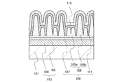
本実施の形態に示す光電変換装置は、導電層上に設けられた第1の導電型である結晶性半導体領域107と、第1の導電型である結晶性半導体領域107上に設けられ、結晶性半導体で形成された複数のウィスカーを有することにより凹凸表面を有し、第1の導電型を付与する不純物元素の濃度勾配を有する真性である結晶性半導体領域109と、凹凸表面を有する結晶性半導体領域109の該凹凸表面を被覆するように設けられた第1の導電型とは逆の第2の導電型である結晶性半導体領域111と、を有する。
The photoelectric conversion device described in this embodiment includes a
図1は、基板101、電極103、第1の導電型である結晶性半導体領域107、真性である結晶性半導体領域109、第1の導電型とは逆である第2の導電型である結晶性半導体領域111、及び絶縁層113を有する光電変換装置である。第1の導電型である結晶性半導体領域107、真性である結晶性半導体領域109、及び第2の導電型である結晶性半導体領域111は光電変換層106として機能する。
FIG. 1 shows a
本実施の形態においては、電極103は、少なくとも導電層104又は混合層105の一方を有する。電極103は、導電層104及び混合層105を有する場合もある。また、電極103の全部が混合層105である場合もある。また、混合層105がない場合もある。電極103が導電層104を有する場合、電極103の導電性を高めることができる。また、電極103と第1の導電型である結晶性半導体領域107との界面が平坦である。また、真性である結晶性半導体領域109は、平坦部と複数のウィスカー(ウィスカー群)を有する。即ち、電極103及び第1の導電型である結晶性半導体領域107の界面は平坦であり、第2の導電型である半導体領域の表面が凹凸状である。さらに、真性である結晶性半導体領域109及び第2の導電型である結晶性半導体領域111の界面が凹凸状であり、第2の導電型である結晶性半導体領域111及び絶縁層113の界面が凹凸状である。
In this embodiment, the
第1の導電型である結晶性半導体領域107は、n型半導体領域及びp型半導体領域の一方であり、第2の導電型である結晶性半導体領域111は、n型半導体領域及びp型半導体領域の他方である。本実施の形態では、第1の導電型である結晶性半導体領域107にp型の結晶性半導体層を用い、第2の導電型である結晶性半導体領域111にn型の結晶性半導体層を用いるが、それぞれ逆の導電型を用いてもよい。
The
基板101は、アルミノシリケートガラス、バリウムホウケイ酸ガラス、アルミノホウケイ酸ガラス等に代表されるガラス基板、サファイア基板、石英基板等を用いることができる。また、ステンレス等の金属基板等に絶縁膜を形成した基板を用いてもよい。本実施の形態では基板101として、ガラス基板を用いる。
As the
導電層104は、シリコンと反応してシリサイドを形成する金属元素で形成する。または、基板101側に、白金、アルミニウム、銅、チタン、またはシリコン、チタン、ネオジム、スカンジウム、もしくはモリブデンなどの耐熱性を向上させる元素が添加されたアルミニウム合金等に代表される導電性の高い金属元素で形成される層を有し、第1の導電型である結晶性半導体領域107側にシリコンと反応してシリサイドを形成する金属元素で形成される層を有する積層構造としてもよい。シリコンと反応してシリサイドを形成する金属元素としては、ジルコニウム、チタン、ハフニウム、バナジウム、ニオブ、タンタル、クロム、モリブデン、コバルト、ニッケル等がある。
The
混合層105は、導電層104を形成する金属元素及びシリコンで形成されてもよい。なお、混合層105が導電層104を形成する金属元素及びシリコンで形成される場合、LPCVD法で第1の導電型である結晶性半導体領域を形成する際の加熱により、原料ガスの活性種が堆積部に供給されるため、導電層104にシリコンが拡散し、混合層105が形成される。
The
導電層104をシリコンと反応してシリサイドを形成する金属元素で形成する場合、混合層105には、シリサイドを形成する金属元素のシリサイド、代表的には、ジルコニウムシリサイド、チタンシリサイド、ハフニウムシリサイド、バナジウムシリサイド、ニオブシリサイド、タンタルシリサイド、クロムシリサイド、モリブデンシリサイド、コバルトシリサイド、及びニッケルシリサイドの一以上が形成される。または、シリサイドを形成する金属元素及びシリコンの合金層が形成される。
When the
導電層104及び第1の導電型である結晶性半導体領域107の間に混合層105を有する場合、導電層104及び第1の導電型である結晶性半導体領域107の間の界面における抵抗を低減させることが可能であるため、導電層104上に直接第1の導電型である結晶性半導体領域107を積層する場合と比較して、直列抵抗を低減することができる。また、導電層104及び第1の導電型である結晶性半導体領域107の密着性を高めることが可能であり、この結果光電変換装置の歩留まりを向上させることができる。
When the
なお、導電層104は箔状、板状、網状であってもよい。このような形状の場合、導電層104は単独で形状保持できるため、基板101を用いる必要はない。このため、コスト削減が可能である。また、導電層104を箔状とすることで、可撓性を有する光電変換装置を作製することができる。
Note that the
第1の導電型である結晶性半導体領域107は、代表的には、導電型を付与する不純物元素が添加された半導体で形成される。半導体材料としては、生産性や価格などの点でシリコンを用いるのが好適である。半導体材料としてシリコンを用いる場合、導電型を付与する不純物元素としては、n型を付与するリンまたはヒ素、p型を付与するホウ素が採用される。ここでは、第1の導電型である結晶性半導体領域107として、p型の結晶性半導体で形成する。
The
なお、本実施の形態では、第1の導電型をp型としているが、第1の導電型をn型としてもよい。 In the present embodiment, the first conductivity type is p-type, but the first conductivity type may be n-type.
真性である結晶性半導体領域109は、結晶性半導体領域109aと、当該結晶性半導体領域109a上に結晶性半導体で形成されるウィスカー109bを複数有するウィスカー群とを有する。なお、結晶性半導体領域109a及びウィスカー109bは、界面が明確ではない。このため、ウィスカー109bの間に形成される谷のうち最も深い谷の底を通り、かつ電極103の表面と平行な平面を、結晶性半導体領域109aとウィスカー109bとの界面とする。本実施の形態に示す光電変換装置は、上記ウィスカーを1つ以上有する。
The intrinsic
結晶性半導体領域109aは、第1の導電型である結晶性半導体領域107を覆う。また、ウィスカー109bは、ひげ状の突起を複数有し、複数の突起が散在している。なお、ウィスカー109bは、円柱状、角柱状等の柱状、円錐状または角錐状の針状でもよい。ウィスカー109bは、頂部が湾曲していてもよい。ウィスカー109bの径は、100nm以上10μm以下、好ましくは500nm以上3μm以下である。また、ウィスカー109bの軸における長さは、300nm以上20μm以下、好ましくは500nm以上15μm以下である。
The
なお、ウィスカー109bの軸における長さhとは、ウィスカー109bの頂点(または上面の中心)を通る軸における、該頂点(または該上面の中心)と結晶性半導体領域109aとの距離である。また、真性である結晶性半導体領域109の厚さは、結晶性半導体領域109aの厚さと、ウィスカー109bの頂点から結晶性半導体領域109aまでの垂線の長さ(すなわち、高さ)の和となる。また、ウィスカー109bの径とは、結晶性半導体領域109aとウィスカー109bとの界面における、輪切り断面形状の長軸の長さをさす。
Note that the length h in the axis of the
なお、ウィスカー109bが結晶性半導体領域109aから伸張する方向を長手方向といい、長手方向に沿った断面形状を長手断面形状という。また、長手方向が法線方向となる面を輪切り断面形状という。
Note that a direction in which the
図1において、真性である結晶性半導体領域109に含まれるウィスカー109bの長手方向は一方向、例えば電極103の表面に対する法線方向に伸張している。なお、ウィスカー109bの長手方向は、電極103の表面に対して法線方向と、略一致していればよく、その場合、方向の差は代表的には5度以内であることが好ましい。
In FIG. 1, the longitudinal direction of the
なお、図1においては、真性である結晶性半導体領域109に含まれるウィスカー109bの長手方向は一方向、例えば電極103の表面に対する法線方向に伸張しているが、ウィスカーの長手方向は不揃いであってもよい。代表的には、長手方向が法線方向と略一致するウィスカーと、長手方向が法線方向とは異なるウィスカーとを有してもよい。
In FIG. 1, the longitudinal direction of the
第2の導電型である結晶性半導体領域111は、n型の結晶性半導体で形成される。なお、第2の導電型である結晶性半導体領域111に用いることができる半導体材料は、第1の導電型である結晶性半導体領域107と同様である。
The
本実施の形態では、真性である結晶性半導体領域109及び第2の導電型である結晶性半導体領域111の界面、第2の導電型である結晶性半導体領域111の表面が凹凸状である。このため、第2の導電型である結晶性半導体領域111から入射する光の反射率を低減することができる。さらに、光電変換層106に入射した光は、光閉じ込め効果により光電変換層106で効率よく吸収されるため、光電変換装置の特性を高めることができる。
In this embodiment mode, the interface between the intrinsic
なお、図1における第1の導電型である結晶性半導体領域107から真性である結晶性半導体領域109の方向に、第1の導電型を付与する不純物元素の濃度勾配を有していることが好ましい。言い換えると、結晶性半導体領域107と結晶性半導体領域109との間(接合部分ともいう)に、当該不純物元素の濃度勾配を有していることが好ましい。ただし、結晶性半導体領域107と結晶性半導体領域109との界面が明確でないため、当該濃度勾配が、結晶性半導体領域107内にある場合、結晶性半導体領域109内にある場合、その両方の領域内にある場合、又は別の領域内にある場合を含むものとする。
1 has a concentration gradient of the impurity element imparting the first conductivity type in the direction from the
図6は、図1におけるウィスカーの拡大図である。図6に示すように、結晶性半導体領域107に含まれる第1の導電型を付与する不純物元素(X)の一部が、結晶性半導体領域107から結晶性半導体領域109の方向に移動し、真性である結晶性半導体領域109側から第1の導電型である結晶性半導体領域107に向かって不純物元素(X)の濃度が高くなるような濃度勾配が生じる。すなわち、結晶性半導体領域107の不純物元素の濃度は、結晶性半導体領域109の不純物元素の濃度より高い。
FIG. 6 is an enlarged view of the whisker in FIG. As shown in FIG. 6, part of the impurity element (X) imparting the first conductivity type included in the
このように、結晶性半導体領域107から結晶性半導体領域109の方向に、不純物元素の濃度勾配を有することで、光電変換装置の短絡電流の低下を防止することができる。すなわち、ウィスカー群を含む結晶性半導体領域に欠陥が含まれることにより、少数キャリアの寿命時間が短くなった場合でも、短絡電流が低下してしまうことを防ぐことができる。
As described above, the concentration gradient of the impurity element in the direction from the
なお、上記の濃度勾配は、不純物元素の濃度が連続的に変化している場合に限定されない。例えば、結晶性半導体領域107と結晶性半導体領域109との間に、結晶性半導体領域109よりも不純物元素の濃度が高く、結晶性半導体領域107より不純物元素の濃度が低い部分を有していればよい。
Note that the above concentration gradient is not limited to the case where the concentration of the impurity element continuously changes. For example, there may be a portion between the
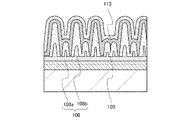
なお、図1においては、第1の導電型である結晶性半導体領域107及び真性である結晶性半導体領域109の界面は平坦であるが、図2に示すように、第1の導電型である結晶性半導体領域108及び真性である結晶性半導体領域109の界面が凹凸状であってもよい。図2に示す第1の導電型である結晶性半導体領域108は、第1の導電型を付与する不純物元素を有する結晶性半導体領域108a、及び当該結晶性半導体領域108a上に設けられ、第1の導電型を付与する不純物元素を有する結晶性半導体で形成されるウィスカー108bを複数有するウィスカー群を有する。なお、結晶性半導体領域108a及びウィスカー108bは、界面が明確ではない。このため、ウィスカー108bの間に形成される谷のうち最も深い谷の底を通り、かつ電極103の表面と平行な平面を、結晶性半導体領域108aとウィスカー108bとの界面とする。
In FIG. 1, the interface between the
ウィスカー108bは、ひげ状の突起を複数有し、複数の突起が散在している。なお、ウィスカー108bは、円柱状、角柱状等の柱状、円錐状または角錐状の針状でもよい。ウィスカー108bは、頂部が湾曲していてもよい。
The
第1の導電型である結晶性半導体領域108に含まれるウィスカー108bの長手方向は一方向、例えば電極103の表面に対する法線方向に伸張している。なお、ウィスカー108bの長手方向は、電極103の表面に対して法線方向と、略一致していればよく、その場合、方向の差は代表的には5度以内であることが好ましい。
The longitudinal direction of the
なお、図2においては、第1の導電型である結晶性半導体領域108に含まれるウィスカー108bの長手方向は一方向、例えば電極103の表面に対する法線方向に伸張しているが、ウィスカーの長手方向は不揃いであってもよい。代表的には、長手方向が法線方向と略一致するウィスカーと、長手方向が法線方向とは異なるウィスカーとを有してもよい。
In FIG. 2, the longitudinal direction of the
図2に示す光電変換装置において、第1の導電型である結晶性半導体領域108及び真性である結晶性半導体領域109の界面、真性である結晶性半導体領域109及び第2の導電型である結晶性半導体領域111の界面、第2の導電型である結晶性半導体領域111の表面が凹凸状である。このため、第2の導電型である結晶性半導体領域111から入射する光の反射率を低減することができる。さらに、光電変換層106に入射した光は、光閉じ込め効果により光電変換層106で効率よく吸収されるため、光電変換装置の特性を高めることができる。
In the photoelectric conversion device illustrated in FIG. 2, the interface between the
なお、図2における第1の導電型である結晶性半導体領域108から真性である結晶性半導体領域109の方向に、第1の導電型を付与する不純物元素の濃度勾配を有していることが好ましい。言い換えると、結晶性半導体領域108と結晶性半導体領域109との間(接合部分ともいう)に、当該不純物元素の濃度勾配を有しているとも言える。ただし、結晶性半導体領域108と結晶性半導体領域109との界面が明確でないため、当該濃度勾配が、結晶性半導体領域108内にある場合、結晶性半導体領域109内にある場合、その両方の領域内にある場合、又は別の領域内にある場合を含むものとする。
2 has a concentration gradient of the impurity element imparting the first conductivity type in the direction from the
図7は、図2におけるウィスカーの拡大図である。図7に示すように、結晶性半導体領域108に含まれる第1の導電型を付与する不純物元素(X)の一部が、結晶性半導体領域108から結晶性半導体領域109の方向に移動し、真性である結晶性半導体領域109側から第1の導電型である結晶性半導体領域107に向かって不純物元素(X)の濃度が高くなるような濃度勾配が生じる。すなわち、結晶性半導体領域108の不純物元素の濃度は、結晶性半導体領域109の不純物元素の濃度より高い。
FIG. 7 is an enlarged view of the whisker in FIG. As shown in FIG. 7, part of the impurity element (X) imparting the first conductivity type included in the
このように、結晶性半導体領域108から結晶性半導体領域109の方向に、不純物元素の濃度勾配を有することで、光電変換装置の短絡電流の低下を防止することができる。すなわち、ウィスカー群を含む結晶性半導体領域に欠陥が含まれることにより、少数キャリアの寿命時間が短くなった場合でも、短絡電流が低下してしまうことを防ぐことができる。
As described above, the concentration gradient of the impurity element in the direction from the
なお、上記の濃度勾配は、不純物元素の濃度が連続的に変化している場合に限定されない。例えば、結晶性半導体領域108と結晶性半導体領域109との間に、結晶性半導体領域109よりも不純物元素の濃度が高く、結晶性半導体領域108より不純物元素の濃度が低い部分を有していればよい。
Note that the above concentration gradient is not limited to the case where the concentration of the impurity element continuously changes. For example, there may be a portion between the
なお、第2の導電型である結晶性半導体領域111の露出部には、保護層の機能及び反射防止機能を有する絶縁層113を形成することが好ましい。
Note that an insulating
絶縁層113には、屈折率が第2の導電型である結晶性半導体領域111の光入射面と空気の中間である材料を用いる。また、第2の導電型である結晶性半導体領域111への光の入射を妨げないように、所定の波長の光に対する透過性を有する材料を用いる。このような材料を用いることで、第2の導電型である結晶性半導体領域111の光入射面における反射を防ぐことができる。なお、このような材料としては、例えば、窒化シリコン、窒化酸化シリコン、フッ化マグネシウムなどがある。
For the insulating
また、第2の導電型である結晶性半導体領域111上に透光性を有する導電層を形成してもよい。透光性を有する導電層としては、インジウム錫酸化物(ITO)、酸化亜鉛(ZnO)、酸化錫(SnO2)、アルミニウムを含む酸化亜鉛等がある。
Alternatively, a light-transmitting conductive layer may be formed over the
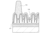
なお、図3に示すように、第2の導電型である結晶性半導体領域111または絶縁層113上に、抵抗を低減するためのグリッド電極115を有してもよい。グリッド電極115は第2の導電型である結晶性半導体領域111の少なくとも一部に接して設ける。例えば、絶縁層113に開口を設けることで、グリッド電極115と第2の導電型である結晶性半導体領域111とを接するように設ける。
Note that, as illustrated in FIG. 3, a
グリッド電極115は、銀、銅、アルミニウム、パラジウム等の金属元素で形成される層で印刷法、ゾルゲル法、塗布法、インクジェット法等を用いて形成する。グリッド電極115を第2の導電型である結晶性半導体領域111に接して設けることで、抵抗損失を低減でき、特に高照度下での電気特性を向上させることができる。
The
次に、図1に示す光電変換装置の作製方法について、図4を用いて説明する。 Next, a method for manufacturing the photoelectric conversion device illustrated in FIG. 1 is described with reference to FIGS.
図4(A)に示すように、基板101上に導電層104を形成する。導電層104は、印刷法、塗布法、インクジェット法、CVD法、スパッタリング法、蒸着法等を適宜用いて形成することができる。なお、導電層104が箔状である場合、基板101を設ける必要はない。また、Roll−to−Rollプロセスを用いることができる。
As shown in FIG. 4A, a
次に、図4(B)に示すように、LPCVD法により第1の導電型である結晶性半導体領域107、真性である結晶性半導体領域109、及び第2の導電型である結晶性半導体領域111を形成する。LPCVD法は、原料ガスとして少なくともシリコンを含む堆積性ガスを用い、LPCVD装置の反応室の圧力を原料ガスを流して保持できる圧力の下限以上200Pa以下として加熱して行う。
Next, as shown in FIG. 4B, the
上記LPCVD法において、加熱温度(成膜温度ともいう)は、LPCVD装置及び導電層104が耐えうる温度以下とし、第1の導電型である結晶性半導体領域107及び真性である結晶性半導体領域109を形成するときは、550℃より高く650℃より低い(すなわち650℃未満の)温度、好ましくは580℃以上650℃未満の温度とする。第2の導電型である結晶性半導体領域111を形成するときは、550℃以下または650℃以上の温度とする。
In the LPCVD method, a heating temperature (also referred to as a film formation temperature) is set to be equal to or lower than a temperature that the LPCVD apparatus and the
上記において、550℃より高く650℃より低い温度、好ましくは580℃以上650℃未満の温度でLPCVD法を用いることにより、結晶性半導体で形成される複数のウィスカーを有する第1の導電型である結晶性半導体領域107、又は結晶性半導体で形成される複数のウィスカーを有する真性である結晶性半導体領域109を形成することができる。それとともに、第1の導電型である結晶性半導体領域107から真性である結晶性半導体領域109の方向に、第1の導電型を付与する不純物元素を移動させることで、第1の導電型である結晶性半導体領域107から真性である結晶性半導体領域109の方向に、第1の導電型を付与する不純物元素の濃度勾配が生じる。
In the above, the first conductivity type having a plurality of whiskers formed of a crystalline semiconductor by using the LPCVD method at a temperature higher than 550 ° C. and lower than 650 ° C., preferably 580 ° C. or higher and lower than 650 ° C. The
上記において、550℃以下または650℃以上の温度でLPCVD法を用いることにより第2の導電型である半導体領域はウィスカーを成長させずに、第2の導電型である結晶性半導体領域111を形成(すなわち堆積)することができる。
In the above, by using the LPCVD method at a temperature of 550 ° C. or lower or 650 ° C. or higher, the second conductive
ウィスカーを成長させずに、第2の導電型である結晶性半導体領域111を形成(すなわち堆積)することにより、複数のウィスカーにより形成された凹凸状の表面における傾斜角を制御することができ、表面における傾斜角を適度に緩和することができる。これにより、後で形成する絶縁層113の被覆性を向上させることができ、且つ第2の導電型である結晶性半導体領域111の表面における光の反射率を低減することができる。
By forming (that is, depositing) the
第2の導電型である結晶性半導体領域111は、成膜温度を550℃以下とすることにより、非晶質半導体又は非晶質半導体と結晶性半導体とが混在した半導体材料を形成することができる。また、成膜温度を650℃以上とすることにより、結晶性半導体を形成することができる。
The
シリコンを含む堆積性ガスとしては、水素化シリコン、フッ化シリコン、または塩化シリコンがあり、代表的には、SiH4、Si2H6、SiF4、SiCl4、Si2Cl6等がある。なお、原料ガスに、水素を導入してもよい。 The deposition gas containing silicon includes silicon hydride, silicon fluoride, or silicon chloride, and typically includes SiH 4 , Si 2 H 6 , SiF 4 , SiCl 4 , Si 2 Cl 6, and the like. Note that hydrogen may be introduced into the source gas.
LPCVD法により第1の導電型である結晶性半導体領域107を形成する際に、導電層104及び第1の導電型である結晶性半導体領域107の間に、混合層105が形成される場合もある。第1の導電型である結晶性半導体領域107の形成工程において、常に原料ガスの活性種が堆積部に供給されるため、第1の導電型である結晶性半導体領域107から導電層104にシリコンが拡散し、混合層105が形成される。混合層105が形成される場合、導電層104及び第1の導電型である結晶性半導体領域107の界面に、低密度領域(粗な領域)が形成されにくくなり、電極103及び第1の導電型である結晶性半導体領域107の界面特性が良好となり、直列抵抗を低減することができる。
When the
第1の導電型である結晶性半導体領域107は、原料ガスとして、シリコンを含む堆積性ガス及びジボランをLPCVD装置の反応室に導入し、550℃より高く650℃より低い温度のLPCVD法により形成する。第1の導電型である結晶性半導体領域107の厚さは5nm以上500nm以下とする。ここでは、第1の導電型である結晶性半導体領域107として、ボロンが添加された結晶性シリコン層を形成する。
The
次に、LPCVD装置の反応室へのジボランの導入を停止し、原料ガスとしてシリコンを含む堆積性ガスをLPCVD装置の反応室に導入し、550℃より高く650℃より低い温度のLPCVD法により、真性である結晶性半導体領域109を形成する。真性である結晶性半導体領域109の厚さは1μm以上20μm以下とする。ここでは、真性である結晶性半導体領域109として、結晶性シリコン層を形成する。この工程において、図6に示すように、第1の導電型である結晶性半導体領域107に含まれるボロン(X)の一部が第1の導電型である結晶性半導体領域107から真性である結晶性半導体領域109の方向に移動し、真性である結晶性半導体領域109側から第1の導電型である結晶性半導体領域107に向かってボロン(X)の濃度が高くなるような濃度勾配が生じる。
Next, the introduction of diborane into the reaction chamber of the LPCVD apparatus is stopped, a deposition gas containing silicon as a source gas is introduced into the reaction chamber of the LPCVD apparatus, and LPCVD at a temperature higher than 550 ° C. and lower than 650 ° C. An intrinsic
次に、原料ガスとしてシリコンを含む堆積性ガス及びホスフィンまたはアルシンをLPCVD装置の反応室に導入するLPCVD法により、第2の導電型である結晶性半導体領域111を形成する。第2の導電型である結晶性半導体領域111の厚さは5nm以上500nm以下とする。ここでは、第2の導電型である結晶性半導体領域111として、リンまたはヒ素が添加されたシリコン層を形成する。
Next, the
以上の工程により、第1の導電型である結晶性半導体領域107、真性である結晶性半導体領域109、及び第2の導電型である結晶性半導体領域111で構成される光電変換層106を形成することができる。
Through the above steps, the
なお、図1に示す光電変換装置の作製工程において、第1の導電型である結晶性半導体領域107にウィスカーが形成される前に、LPCVD装置の反応室へジボランの導入を停止することで、図1に示すように、第1の導電型である結晶性半導体領域107及び真性である結晶性半導体領域109の界面が平坦となる。一方、第1の導電型である結晶性半導体領域108においてウィスカーが形成された後、LPCVD装置の反応室へジボランの導入を停止した場合は、図2に示すように、第1の導電型である結晶性半導体領域108及び真性である結晶性半導体領域109の界面が凹凸状となる。そして、真性である結晶性半導体領域109を形成する工程において、図7に示すように、結晶性半導体領域108に含まれるボロン(X)の一部が結晶性半導体領域108から結晶性半導体領域109の方向に移動し、真性である結晶性半導体領域109側から第1の導電型である結晶性半導体領域108に向かってボロン(X)の濃度が高くなるような濃度勾配が生じる。
Note that in the manufacturing process of the photoelectric conversion device illustrated in FIG. 1, before the whisker is formed in the
また、第1の導電型である結晶性半導体領域107を形成する前に、導電層104の表面をフッ酸で洗浄してもよい。当該工程により、電極103及び第1の導電型である結晶性半導体領域107の密着性を高めることができる。
Alternatively, the surface of the
また、第1の導電型である結晶性半導体領域107、真性である結晶性半導体領域109、及び第2の導電型である結晶性半導体領域111の原料ガスに、ヘリウム、ネオン、アルゴン、キセノン等の希ガス、または窒素を混合してもよい。第1の導電型である結晶性半導体領域107、真性である結晶性半導体領域109、及び第2の導電型である結晶性半導体領域111の原料ガスに希ガスまたは窒素を混合することで、ウィスカーの密度を高めることができる。
Further, helium, neon, argon, xenon, or the like is used as a source gas for the
また、第1の導電型である結晶性半導体領域107、真性である結晶性半導体領域109、及び第2の導電型である結晶性半導体領域111の一以上を形成した後、LPCVD装置の反応室への原料ガスの導入を停止し、真空状態で温度を保持(即ち、真空状態加熱)することで、第1の導電型である結晶性半導体領域107または真性である結晶性半導体領域109に含まれるウィスカーの密度を増加させることができる。
In addition, after forming one or more of the
次に、図4(C)に示すように、第2の導電型である結晶性半導体領域111上に絶縁層113を形成する。絶縁層113は、CVD法、スパッタリング法、蒸着法等で形成することができる。
Next, as illustrated in FIG. 4C, the insulating
以上の工程により、テクスチャー構造の電極を形成せずとも、変換効率の高い光電変換装置を作製することができる。 Through the above steps, a photoelectric conversion device with high conversion efficiency can be manufactured without forming a textured electrode.
(実施の形態2)
本実施の形態では、実施の形態1と比較して、欠陥の少ない光電変換層の作製方法について、説明する。
(Embodiment 2)
In this embodiment, a method for manufacturing a photoelectric conversion layer with fewer defects than that in Embodiment 1 is described.
実施の形態1に示す第1の導電型である結晶性半導体領域107、第1の導電型である結晶性半導体領域108、真性である結晶性半導体領域109、及び第2の導電型である結晶性半導体領域111のいずれか一以上を形成した後、LPCVD装置の反応室の温度を400℃以上450℃以下とすると共に、LPCVD装置への原料ガスの導入を停止し、水素を導入する。次に、水素雰囲気において400℃以上450℃以下の加熱処理を行うことで、第1の導電型である結晶性半導体領域107、第1の導電型である結晶性半導体領域108、真性である結晶性半導体領域109、及び第2の導電型である結晶性半導体領域111のいずれか一以上に含まれるダングリングボンドを水素終端することができる。当該加熱処理を水素化処理ともいう。この結果、第1の導電型である結晶性半導体領域107、第1の導電型である結晶性半導体領域108、真性である結晶性半導体領域109、及び第2の導電型である結晶性半導体領域111のいずれか一以上に含まれる欠陥を低減することができる。この結果、欠陥における光励起キャリアの再結合を低減することが可能であり、光電変換装置の変換効率を高めることができる。
The
なお、上記水素化処理は、少なくとも真性である結晶性半導体領域109を形成した後に行うことが好ましい。この結果、スループットを高めつつ、光電変換装置の変換効率を高めることができる。
Note that the hydrogenation treatment is preferably performed after the
(実施の形態3)
本実施の形態では、光電変換層を複数積層する、いわゆるタンデム構造の光電変換装置の構造について、図5を用いて説明する。なお、本実施の形態では、二つの光電変換層を積層する場合について説明するが、三つ以上の光電変換層を有する積層構造としてもよい。また、以下においては、光入射側の前方光電変換層をトップセルと、後方光電変換層をボトムセルと呼ぶことがある。
(Embodiment 3)
In this embodiment, a structure of a so-called tandem photoelectric conversion device in which a plurality of photoelectric conversion layers are stacked is described with reference to FIGS. Note that although a case where two photoelectric conversion layers are stacked is described in this embodiment, a stacked structure including three or more photoelectric conversion layers may be employed. In the following, the front photoelectric conversion layer on the light incident side may be referred to as a top cell, and the rear photoelectric conversion layer may be referred to as a bottom cell.
図5に示す光電変換装置は、基板101と、電極103と、ボトムセルである光電変換層106と、トップセルである光電変換層120と、絶縁層113が積層された構造を有する。ここで、光電変換層106は、実施の形態1に示す第1の導電型である結晶性半導体領域107、真性である結晶性半導体領域109、及び第2の導電型である結晶性半導体領域111で構成される。また、光電変換層120は、第3の導電型である半導体領域121と、真性である半導体領域123と、第4の導電型である半導体領域125との積層構造で構成される。上記光電変換層106に用いられる真性である結晶性半導体領域109と、光電変換層120に用いられる真性である半導体領域123のバンドギャップは異なるものであることが望ましい。バンドギャップが異なる半導体を用いることで、広い波長域にわたる光を吸収することが可能になるため、光電変換効率を向上させることができる。
The photoelectric conversion device illustrated in FIG. 5 has a structure in which a
例えば、トップセルにはバンドギャップの大きい半導体を、ボトムセルにはバンドギャップの小さい半導体を用いることができる。もちろん、その逆の構成とすることも可能である。ここでは、一例として、ボトムセルである光電変換層106に結晶性半導体(代表的には、結晶性シリコン)を採用し、トップセルである光電変換層120に非晶質半導体(代表的には、非晶質シリコン)を採用する構成について示す。
For example, a semiconductor having a large band gap can be used for the top cell, and a semiconductor having a small band gap can be used for the bottom cell. Of course, the reverse configuration is also possible. Here, as an example, a crystalline semiconductor (typically, crystalline silicon) is used for the
なお、本実施の形態では、光が絶縁層113から入射する構成について示すが、開示する発明の一態様はこれに限定されない。基板101の裏面側(図の下方)側から光が入射する構成としてもよい。
Note that although a structure in which light enters from the insulating
基板101、電極103、光電変換層106、絶縁層113の構成については、先の実施の形態に示す構成と同様であるため、ここでは省略する。
The structures of the
トップセルである光電変換層120において、第3の導電型である半導体領域121および第4の導電型である半導体領域125としては、代表的には、導電型を付与する不純物元素が添加された半導体材料を含む半導体層が採用される。半導体材料などの詳細は、実施の形態1に示す第1の導電型である結晶性半導体領域107と同様である。本実施の形態では、半導体材料としてシリコンを用い、第3の導電型としてp型を、第4の導電型としてn型を適用する場合について示す。また、その結晶性は非晶質とする。もちろん、第3の導電型としてn型を、第4の導電型としてp型を適用することも可能であり、他の結晶性の半導体層を用いることも可能である。
In the
真性である半導体領域123としては、シリコン、炭化シリコン、ゲルマニウム、ガリウムヒ素、リン化インジウム、セレン化亜鉛、窒化ガリウム、シリコンゲルマニウムなどが用いられる。他に、有機材料を含む半導体材料や、金属酸化物半導体材料などを用いることも可能である。
As the
本実施の形態では、真性である半導体領域123に非晶質シリコンを用いる。もちろん、シリコン以外の半導体材料であって、ボトムセルの真性である結晶性半導体領域109とはバンドギャップの異なるものを用いて形成してもよい。ここで、真性である半導体領域123の厚さは、真性である結晶性半導体領域109の厚さより小さいことが望ましく、代表的には50nm以上1000nm以下、望ましくは、100nm以上450nm以下である。
In this embodiment mode, amorphous silicon is used for the
第3の導電型である半導体領域121、真性である半導体領域123、及び第4の導電型である半導体領域125の形成方法としては、プラズマCVD法、LPCVD法などがある。プラズマCVD法を用いる場合には、例えば、プラズマCVD装置の反応室の圧力を代表的には10Pa以上1332Pa以下とし、原料ガスとしてシリコンを含む堆積性ガス及び水素を反応室に導入し、電極に高周波電力を供給して、グロー放電させることで、真性である半導体領域123を形成することができる。第3の導電型である半導体領域121は、上記原料ガスに更にジボランを添加することで形成することができる。第3の導電型である半導体領域121は、1nm以上100nm以下、望ましくは、5nm以上50nm以下の厚さとなるように形成する。第4の導電型である半導体領域125は、上記原料ガスに更にホスフィンまたはアルシンを添加することで形成することができる。第4の導電型である半導体領域125は、1nm以上100nm以下、望ましくは、5nm以上50nm以下の厚さとなるように形成する。
As a method for forming the
また、第3の導電型である半導体領域121として、導電型を付与する不純物元素が添加されていない非晶質シリコン層をプラズマCVD法またはLPCVD法などによって形成した上で、イオン注入などの方法でボロンを添加して、第3の導電型である半導体領域121を形成してもよい。第4の導電型である半導体領域125として、導電型を付与する不純物元素が添加されていない非晶質シリコン層をプラズマCVD法またはLPCVD法などによって形成した上で、イオン注入などの方法でリンまたはヒ素を添加して、第4の導電型である半導体領域125を形成してもよい。
Further, as the
上述のように、光電変換層120に非晶質シリコンを適用することで、800nm未満の波長の光を効果的に吸収して光電変換することが可能となる。また、光電変換層106に結晶性シリコンを適用することで、より長波長(例えば1200nm程度まで)の光を吸収して光電変換することが可能となる。このように、バンドギャップの異なる光電変換層を積層した構造(いわゆるタンデム型の構造)とすることで、光電変換効率を大きく向上させることができる。
As described above, by applying amorphous silicon to the
なお、本実施の形態では、トップセルとしてバンドギャップの大きい非晶質シリコンを用い、ボトムセルとしてバンドギャップの小さい結晶性シリコンを用いているが、開示する発明の一態様はこれに限定されない。バンドギャップの異なる半導体材料を適宜組み合わせて、トップセルおよびボトムセルを構成することができる。また、トップセルとボトムセルの構成を入れ替えて光電変換装置を構成することも可能である。さらに、三層以上の光電変換層の積層構造とすることも可能である。 Note that although amorphous silicon having a large band gap is used for the top cell and crystalline silicon having a small band gap is used for the bottom cell in this embodiment, one embodiment of the disclosed invention is not limited thereto. A top cell and a bottom cell can be formed by appropriately combining semiconductor materials having different band gaps. Further, it is possible to configure the photoelectric conversion device by switching the configurations of the top cell and the bottom cell. Furthermore, it is possible to have a laminated structure of three or more photoelectric conversion layers.
以上の構成により、光電変換装置の変換効率を高めることができる。 With the above structure, the conversion efficiency of the photoelectric conversion device can be increased.
(実施の形態4)
本実施の形態では、光電変換装置の第2の導電型である半導体領域上に湿式法により導電層を形成した例について、図8を用いて説明する。
(Embodiment 4)
In this embodiment, an example in which a conductive layer is formed by a wet method over a semiconductor region which is the second conductivity type of the photoelectric conversion device will be described with reference to FIGS.
図8は、基板101、電極103、第1の導電型である結晶性半導体領域107、真性である結晶性半導体領域109、第1の導電型とは逆の第2の導電型である結晶性半導体領域111、及び導電層213を有する光電変換装置である。第1の導電型である結晶性半導体領域107、真性である結晶性半導体領域109、及び第2の導電型である結晶性半導体領域111は光電変換層106として機能する。
FIG. 8 shows a
電極103は、導電層104と、混合層105を有する場合もある。また、電極103と第1の導電型である結晶性半導体領域107との界面が平坦である。また、真性である結晶性半導体領域109は、複数のウィスカー(ウィスカー群)を有する。したがって、真性である結晶性半導体領域109及び第2の導電型である結晶性半導体領域111の界面および第2の導電型である結晶性半導体領域111の表面が凹凸状である。
The
本実施の形態では、第2の導電型である結晶性半導体領域111上の一部または全部に導電層213を湿式法により形成する。これにより、ウィスカーが形成されたことにより、凹凸化した表面を有する第2の導電型である結晶性半導体領域111の表面にカバレッジよく導電層213を形成することができる。ウィスカーが形成されたことにより、凹凸化した表面を有する第2の導電型である結晶性半導体領域111上に、湿式法により導電層213を形成することで、光入射面側の抵抗を下げることができる。また、導電層213を電極として用いてもよい。導電層213に用いる材料は、光電変換層106として機能する半導体領域が吸収しうる波長領域の光に対して透光性を有する材料であることが好ましい。
In this embodiment mode, the
湿式法としては、ディップコート法、スピンコート法、スプレイコート法、インクジェット法、印刷法等の塗布法等を用いることができる。他に、電解メッキ法、無電解メッキ法等を用いることができる。 As the wet method, a dip coating method, a spin coating method, a spray coating method, an inkjet method, a coating method such as a printing method, or the like can be used. In addition, an electrolytic plating method, an electroless plating method, or the like can be used.
塗布法に用いる塗布液は、導電材料を含む液体、ゾルまたはゲルなどの液状体を用いることができる。導電材料としては、インジウム錫酸化物、酸化亜鉛、酸化錫、アルミニウムを含む酸化亜鉛等の透光性導電材料である金属酸化物の微粒子、金(Au)、白金(Pt)、ニッケル(Ni)、タングステン(W)、クロム(Cr)、モリブデン(Mo)、鉄(Fe)、コバルト(Co)、銅(Cu)、パラジウム(Pd)、銀(Ag)等の金属の微粒子、導電性ポリアニリン、導電性ポリピロール、導電性ポリチオフェン、ポリエチレンジオキシチオフェン(PEDOT)とポリスチレンスルホン酸(PSS)等の導電性高分子等を用いることができる。導電材料として微粒子を用いる場合は、分散性を向上させるために該微粒子の表面に有機物などをコーティングして使うこともできる。導電材料を含む液体の溶媒(または分散媒)としては、水の他、アルコール類、炭化水素系化合物、エーテル系化合物等を用いることができる。これらの溶媒(または分散媒)は、単独で用いてもよく、2種類以上混合して用いてもよい。 As a coating solution used in the coating method, a liquid containing a conductive material, or a liquid such as sol or gel can be used. The conductive material includes indium tin oxide, zinc oxide, tin oxide, metal oxide fine particles that are light-transmitting conductive materials such as zinc oxide containing aluminum, gold (Au), platinum (Pt), nickel (Ni). Fine particles of metals such as tungsten (W), chromium (Cr), molybdenum (Mo), iron (Fe), cobalt (Co), copper (Cu), palladium (Pd), silver (Ag), conductive polyaniline, Conductive polymers such as conductive polypyrrole, conductive polythiophene, polyethylenedioxythiophene (PEDOT) and polystyrenesulfonic acid (PSS) can be used. When fine particles are used as the conductive material, the surface of the fine particles can be coated with an organic substance or the like in order to improve dispersibility. As a liquid solvent (or dispersion medium) containing a conductive material, alcohols, hydrocarbon compounds, ether compounds, and the like can be used in addition to water. These solvents (or dispersion media) may be used alone or in combination of two or more.
湿式法として塗布法を用いる場合は、導電材料を含む液体又は液状体を塗布し、乾燥、焼成することにより導電層213を形成することができる。湿式法として塗布法を用いる場合は、導電層213を容易に厚膜化することができ、導電層213を低抵抗化することができる。
In the case where an application method is used as the wet method, the
導電層213を厚膜化した場合には、導電層213の表面は平坦化される。この場合、導電層213の表面を凹凸状に加工してもよい。表面を凹凸状に加工することで、入射する光の反射率を低減することができ、また、光閉じ込め効果により光電変換装置の特性を高めることができる。
When the
また、導電層213を形成する前に、第2の導電型である結晶性半導体領域111上の一部又は全部に別の導電層(図示せず)を形成してもよい。例えば、導電層213を形成する前に、CVD法、スパッタリング法、蒸着法等の乾式法を用いて、インジウム錫酸化物、酸化亜鉛、酸化錫、アルミニウムを含む酸化亜鉛等の透光性導電材料からなる導電層を形成してもよい。予め別の導電層を形成することで、第2の導電型である結晶性半導体領域111の表面を保護することができる。また、予め別の導電層を形成することで、導電層213と第2の導電型である結晶性半導体領域111との密着性を向上させることができる。
Further, before the
また、導電層213として、導電性を有する液体(電解質を含む液体)を第2の導電型である結晶性半導体領域111上にウィスカーの隙間を充填するように設けて、これを電極として用いてもよい。この場合は、基板101と基板101に対向する第2の基板との間に導電性を有する液体を封入し、封止材で封止することで導電層213を形成することができる。いずれにしても、ウィスカーの隙間を充填するような電極を設けることで、光入射面の抵抗を下げることができる。
In addition, as the
本実施の形態は、他の実施の形態と適宜組み合わせて実施することができる。 This embodiment can be implemented in appropriate combination with any of the other embodiments.
本実施例では、チタン箔、及びチタン箔上にポリシリコンで形成されるウィスカー群を有する試料の正反射率の違いについて、説明する。 In this example, a difference in regular reflectance between a titanium foil and a sample having a whisker group formed of polysilicon on the titanium foil will be described.
はじめに、試料の作製方法について、説明する。 First, a method for manufacturing a sample is described.
<試料1>
試料1は、直径φ12mmの円形状に切断された厚さ0.1mmのチタン箔を用いた。
<Sample 1>
Sample 1 used was a 0.1 mm thick titanium foil cut into a circular shape having a diameter of 12 mm.
<試料2>
試料1と同様の形状である直径φ12mm及び厚さ0.1mmのチタン箔上に、LPCVD法により、ウィスカー群を有するポリシリコン層を形成した。ここでのポリシリコン層の成膜条件は、圧力13Pa、基板温度600℃に設定した処理室に、流量300sccmのシランを導入し、2時間15分ポリシリコン層を堆積した。
<
A polysilicon layer having a whisker group was formed by LPCVD on a titanium foil having the same shape as that of Sample 1 and having a diameter of 12 mm and a thickness of 0.1 mm. Here, the polysilicon layer was formed by introducing silane at a flow rate of 300 sccm into a processing chamber set at a pressure of 13 Pa and a substrate temperature of 600 ° C., and depositing the polysilicon layer for 2 hours and 15 minutes.
次に、試料1及び試料2それぞれの正反射率を分光光度計(日立ハイテク社製「日立分光光度計 U−4100」)により測定した結果を図9に示す。ここでは、サンプリング間隔を2nmとして、波長が200nmから1200nmまでの光を各試料に照射した。また、各試料への光の入射角度を5度として、測定された反射率(5度正反射率)を測定した。試料1の反射率を破線501で示し、試料2の反射率を実線502で示す。横軸を照射光の波長とし、縦軸を反射率とする。
Next, FIG. 9 shows the results of measuring the specular reflectance of each of Sample 1 and
図9から、チタン箔表面にウィスカー群を有するポリシリコン層が形成された試料2は光の反射率の最大値が0.14%と極めて低く、ほとんど光の反射が生じていない。なお、波長850nmから894nmの範囲では、SN比が小さいため、反射率がマイナスとなっている。一方、チタン箔である試料1は、正反射率が2%から15%である。以上のことから、チタン箔表面にウィスカー群を有するポリシリコン層を形成することで、反射率を低減することができることがわかる。
From FIG. 9, the
101 基板
103 電極
104 導電層
105 混合層
106 光電変換層
107 結晶性半導体領域
108 結晶性半導体領域
108a 結晶性半導体領域
108b ウィスカー
109 結晶性半導体領域
109a 結晶性半導体領域
109b ウィスカー
111 結晶性半導体領域
113 絶縁層
115 グリッド電極
120 光電変換層
121 半導体領域
123 半導体領域
125 半導体領域
213 導電層
501 破線
502 実線
101
Claims (2)
前記第1の半導体領域上に、低圧化学的気相堆積法により、第2の半導体領域を形成するとともに、前記第1の半導体領域から前記第2の半導体領域の方向に、前記第1の導電型を付与する不純物元素を移動させ、A second semiconductor region is formed on the first semiconductor region by low pressure chemical vapor deposition, and the first conductive region extends from the first semiconductor region to the second semiconductor region. Move the impurity element that gives the mold,
前記第2の半導体領域上に、低圧化学的気相堆積法により、第2の導電型を付与する不純物元素を含む第3の半導体領域を形成し、Forming a third semiconductor region containing an impurity element imparting the second conductivity type on the second semiconductor region by low-pressure chemical vapor deposition;
前記第1の半導体領域の形成は、シリコンを含む堆積性ガス及び前記第1の導電型を付与する不純物元素を含むガスを原料ガスに用いて行い、The first semiconductor region is formed using a deposition gas containing silicon and a gas containing an impurity element imparting the first conductivity type as a source gas,
前記第1の半導体領域の形成は、550℃より高く650℃より低い温度で行い、The first semiconductor region is formed at a temperature higher than 550 ° C. and lower than 650 ° C.,
前記第2の半導体領域の形成は、シリコンを含む堆積性ガスを原料ガスに用いて行い、The second semiconductor region is formed using a deposition gas containing silicon as a source gas,
前記第2の半導体領域の形成は、550℃より高く650℃より低い温度で行い、The second semiconductor region is formed at a temperature higher than 550 ° C. and lower than 650 ° C.
前記第3の半導体領域の形成は、シリコンを含む堆積性ガス及び前記第2の導電型を付与する不純物元素を含むガスを原料ガスに用いて行い、The third semiconductor region is formed using a deposition gas containing silicon and a gas containing an impurity element imparting the second conductivity type as a source gas,
前記第3の半導体領域の形成は、550℃以下または650℃以上の温度で行い、The third semiconductor region is formed at a temperature of 550 ° C. or lower or 650 ° C. or higher,
前記第1の半導体領域は、結晶性を有し、The first semiconductor region has crystallinity,
前記第2の半導体領域は、結晶性を有し、The second semiconductor region has crystallinity,
前記第2の半導体領域は、複数の突起を有することを特徴とする光電変換装置の作製方法。The method for manufacturing a photoelectric conversion device, wherein the second semiconductor region includes a plurality of protrusions.
前記第1の半導体領域上に、低圧化学的気相堆積法により、第2の半導体領域を形成するとともに、前記第1の半導体領域から前記第2の半導体領域の方向に、前記第1の導電型を付与する不純物元素を移動させ、A second semiconductor region is formed on the first semiconductor region by low pressure chemical vapor deposition, and the first conductive region extends from the first semiconductor region to the second semiconductor region. Move the impurity element that gives the mold,
前記第2の半導体領域上に、低圧化学的気相堆積法により、第2の導電型を付与する不純物元素を含む第3の半導体領域を形成し、Forming a third semiconductor region containing an impurity element imparting the second conductivity type on the second semiconductor region by low-pressure chemical vapor deposition;
前記第1の半導体領域の形成は、シリコンを含む堆積性ガス及び前記第1の導電型を付与する不純物元素を含むガスを原料ガスに用いて行い、The first semiconductor region is formed using a deposition gas containing silicon and a gas containing an impurity element imparting the first conductivity type as a source gas,
前記第1の半導体領域の形成は、550℃より高く650℃より低い温度で行い、The first semiconductor region is formed at a temperature higher than 550 ° C. and lower than 650 ° C.,
前記第2の半導体領域の形成は、シリコンを含む堆積性ガスを原料ガスに用いて行い、The second semiconductor region is formed using a deposition gas containing silicon as a source gas,
前記第2の半導体領域の形成は、550℃より高く650℃より低い温度で行い、The second semiconductor region is formed at a temperature higher than 550 ° C. and lower than 650 ° C.
前記第3の半導体領域の形成は、シリコンを含む堆積性ガス及び前記第2の導電型を付与する不純物元素を含むガスを原料ガスに用いて行い、The third semiconductor region is formed using a deposition gas containing silicon and a gas containing an impurity element imparting the second conductivity type as a source gas,
前記第3の半導体領域の形成は、550℃以下または650℃以上の温度で行い、The third semiconductor region is formed at a temperature of 550 ° C. or lower or 650 ° C. or higher,
前記第1の半導体領域は、結晶性を有し、The first semiconductor region has crystallinity,
前記第2の半導体領域は、結晶性を有し、The second semiconductor region has crystallinity,
前記第1の半導体領域は、複数の突起を有することを特徴とする光電変換装置の作製方法。The method for manufacturing a photoelectric conversion device, wherein the first semiconductor region includes a plurality of protrusions.
Priority Applications (1)
| Application Number | Priority Date | Filing Date | Title |
|---|---|---|---|
| JP2011132818A JP5656330B2 (en) | 2010-06-18 | 2011-06-15 | Method for manufacturing photoelectric conversion device |
Applications Claiming Priority (3)
| Application Number | Priority Date | Filing Date | Title |
|---|---|---|---|
| JP2010140005 | 2010-06-18 | ||
| JP2010140005 | 2010-06-18 | ||
| JP2011132818A JP5656330B2 (en) | 2010-06-18 | 2011-06-15 | Method for manufacturing photoelectric conversion device |
Publications (3)
| Publication Number | Publication Date |
|---|---|
| JP2012023350A JP2012023350A (en) | 2012-02-02 |
| JP2012023350A5 JP2012023350A5 (en) | 2014-07-17 |
| JP5656330B2 true JP5656330B2 (en) | 2015-01-21 |
Family
ID=45329032
Family Applications (1)
| Application Number | Title | Priority Date | Filing Date |
|---|---|---|---|
| JP2011132818A Expired - Fee Related JP5656330B2 (en) | 2010-06-18 | 2011-06-15 | Method for manufacturing photoelectric conversion device |
Country Status (2)
| Country | Link |
|---|---|
| US (1) | US8569098B2 (en) |
| JP (1) | JP5656330B2 (en) |
Families Citing this family (7)
| Publication number | Priority date | Publication date | Assignee | Title |
|---|---|---|---|---|
| WO2011158722A1 (en) * | 2010-06-18 | 2011-12-22 | Semiconductor Energy Laboratory Co., Ltd. | Photoelectric conversion device and manufacturing method thereof |
| US9076909B2 (en) | 2010-06-18 | 2015-07-07 | Semiconductor Energy Laboratory Co., Ltd. | Photoelectric conversion device and method for manufacturing the same |
| KR20130006301A (en) * | 2011-07-08 | 2013-01-16 | 가부시키가이샤 한도오따이 에네루기 켄큐쇼 | Method for forming silicon film and method for manufacturing power storage device |
| JP6065366B2 (en) * | 2012-01-30 | 2017-01-25 | 富士通セミコンダクター株式会社 | Manufacturing method of semiconductor device |
| US9227259B2 (en) * | 2012-08-22 | 2016-01-05 | International Business Machines Corporation | Increasing the efficiency of solar cells by transfer of solder |
| TWI474499B (en) | 2012-10-12 | 2015-02-21 | Iner Aec Executive Yuan | Microcrystalline silicon thin film solar cell element and its manufacturing method |
| JP7337756B2 (en) * | 2020-07-30 | 2023-09-04 | 株式会社東芝 | semiconductor equipment |
Family Cites Families (19)
| Publication number | Priority date | Publication date | Assignee | Title |
|---|---|---|---|---|
| JP3203709B2 (en) * | 1991-10-14 | 2001-08-27 | ソニー株式会社 | Semiconductor device having floating gate and method of manufacturing the same |
| JPH07235611A (en) * | 1994-02-21 | 1995-09-05 | Oki Electric Ind Co Ltd | Capacitor of semiconductor memory storage and manufacture thereof |
| JPH10242417A (en) * | 1997-02-25 | 1998-09-11 | Oki Electric Ind Co Ltd | Semiconductor device and its manufacturing method |
| JP2001068708A (en) * | 1999-08-30 | 2001-03-16 | Sanyo Electric Co Ltd | Semiconductor element, solar-battery element and manufacture of the semiconductor element |
| JP2003069061A (en) | 2001-08-24 | 2003-03-07 | Sharp Corp | Laminated photovoltaic transducer device |
| JP2003258285A (en) | 2002-02-27 | 2003-09-12 | Sharp Corp | Manufacturing method of rugged surface structure and solar battery |
| JP2004014958A (en) * | 2002-06-11 | 2004-01-15 | Fuji Electric Holdings Co Ltd | Thin film polycrystalline solar cell and manufacturing method therefor |
| JP4140765B2 (en) | 2002-09-19 | 2008-08-27 | コバレントマテリアル株式会社 | Acicular silicon crystal and method for producing the same |
| WO2004102677A1 (en) * | 2003-05-13 | 2004-11-25 | Asahi Glass Company, Limited | Transparent conductive substrate for solar battery and method for producing same |
| JP4480525B2 (en) * | 2003-09-12 | 2010-06-16 | 三洋電機株式会社 | Photovoltaic device |
| JP2005150614A (en) | 2003-11-19 | 2005-06-09 | Sharp Corp | Solar battery, and manufacturing method thereof |
| JP5058084B2 (en) * | 2007-07-27 | 2012-10-24 | 株式会社半導体エネルギー研究所 | Method for manufacturing photoelectric conversion device and microwave plasma CVD apparatus |
| JP5438986B2 (en) | 2008-02-19 | 2014-03-12 | 株式会社半導体エネルギー研究所 | Method for manufacturing photoelectric conversion device |
| JP2012023343A (en) | 2010-06-18 | 2012-02-02 | Semiconductor Energy Lab Co Ltd | Photoelectric conversion device and method of producing the same |
| JP5894379B2 (en) | 2010-06-18 | 2016-03-30 | 株式会社半導体エネルギー研究所 | Photoelectric conversion device |
| TWI514599B (en) | 2010-06-18 | 2015-12-21 | Semiconductor Energy Lab | Photoelectric conversion device and manufacturing method thereof |
| WO2011158722A1 (en) | 2010-06-18 | 2011-12-22 | Semiconductor Energy Laboratory Co., Ltd. | Photoelectric conversion device and manufacturing method thereof |
| JP2012023342A (en) | 2010-06-18 | 2012-02-02 | Semiconductor Energy Lab Co Ltd | Photoelectric conversion device and method of producing the same |
| US9076909B2 (en) | 2010-06-18 | 2015-07-07 | Semiconductor Energy Laboratory Co., Ltd. | Photoelectric conversion device and method for manufacturing the same |
-
2011
- 2011-06-10 US US13/157,593 patent/US8569098B2/en active Active
- 2011-06-15 JP JP2011132818A patent/JP5656330B2/en not_active Expired - Fee Related
Also Published As
| Publication number | Publication date |
|---|---|
| JP2012023350A (en) | 2012-02-02 |
| US8569098B2 (en) | 2013-10-29 |
| US20110312121A1 (en) | 2011-12-22 |
Similar Documents
| Publication | Publication Date | Title |
|---|---|---|
| JP5656330B2 (en) | Method for manufacturing photoelectric conversion device | |
| US9397245B2 (en) | Photoelectric conversion device and manufacturing method thereof | |
| JP6125594B2 (en) | Method for manufacturing photoelectric conversion device | |
| KR20130084218A (en) | Nanostructure and photovoltaic cell implementing same | |
| US9076909B2 (en) | Photoelectric conversion device and method for manufacturing the same | |
| JP2014103259A (en) | Solar cell, solar cell module, and method of manufacturing the same | |
| TW201733150A (en) | Method for manufacturing photoelectric conversion device | |
| JP5894379B2 (en) | Photoelectric conversion device | |
| CN116914012A (en) | Double-sided doped polycrystalline silicon passivation contact battery and preparation method thereof | |
| CN116995111A (en) | Heterojunction solar cell and preparation method thereof | |
| US20110308600A1 (en) | Photoelectric conversion device and method for manufacturing the same | |
| US20100224238A1 (en) | Photovoltaic cell comprising an mis-type tunnel diode | |
| KR20200125067A (en) | Manufacturing method of heterojunction solar cell | |
| JP6143520B2 (en) | Crystalline silicon solar cell and manufacturing method thereof | |
| TWI483405B (en) | Photovoltaic cell and method of manufacturing a photovoltaic cell | |
| CN117276360B (en) | Novel crystalline silicon heterojunction solar cell structure and preparation method and application thereof | |
| CN220604704U (en) | Double-sided doped polycrystalline silicon passivation contact battery | |
| Jiat et al. | Current transportation enhancement with ZnO nanoroads for silicon nanowire solar cell | |
| CN217606831U (en) | High-efficiency heterojunction solar cell | |
| JP6097068B2 (en) | SOLAR CELL, MANUFACTURING METHOD THEREOF, AND SOLAR CELL MODULE | |
| CN113394309A (en) | Solar cell and preparation method thereof | |
| JP2024533257A (en) | Methods and systems for photovoltaic devices using silicon particles - Patents.com | |
| KR20120059371A (en) | Thin film type solar cell using glass substrate with surface texture and preparation method thereof | |
| CN107403852A (en) | Silicon substrate heterojunction solar cell and its manufacturing method thereof | |
| JP2013098390A (en) | Photoelectric transducer, manufacturing method thereof, and photoelectric conversion module |
Legal Events
| Date | Code | Title | Description |
|---|---|---|---|
| A521 | Request for written amendment filed |
Free format text: JAPANESE INTERMEDIATE CODE: A523 Effective date: 20140529 |
|
| A621 | Written request for application examination |
Free format text: JAPANESE INTERMEDIATE CODE: A621 Effective date: 20140529 |
|
| TRDD | Decision of grant or rejection written | ||
| A01 | Written decision to grant a patent or to grant a registration (utility model) |
Free format text: JAPANESE INTERMEDIATE CODE: A01 Effective date: 20141118 |
|
| A977 | Report on retrieval |
Free format text: JAPANESE INTERMEDIATE CODE: A971007 Effective date: 20141119 |
|
| A61 | First payment of annual fees (during grant procedure) |
Free format text: JAPANESE INTERMEDIATE CODE: A61 Effective date: 20141124 |
|
| R150 | Certificate of patent or registration of utility model |
Ref document number: 5656330 Country of ref document: JP Free format text: JAPANESE INTERMEDIATE CODE: R150 |
|
| R250 | Receipt of annual fees |
Free format text: JAPANESE INTERMEDIATE CODE: R250 |
|
| R250 | Receipt of annual fees |
Free format text: JAPANESE INTERMEDIATE CODE: R250 |
|
| R250 | Receipt of annual fees |
Free format text: JAPANESE INTERMEDIATE CODE: R250 |
|
| R250 | Receipt of annual fees |
Free format text: JAPANESE INTERMEDIATE CODE: R250 |
|
| R250 | Receipt of annual fees |
Free format text: JAPANESE INTERMEDIATE CODE: R250 |
|
| R250 | Receipt of annual fees |
Free format text: JAPANESE INTERMEDIATE CODE: R250 |
|
| LAPS | Cancellation because of no payment of annual fees |