JP5058084B2 - Method for manufacturing photoelectric conversion device and microwave plasma CVD apparatus - Google Patents
Method for manufacturing photoelectric conversion device and microwave plasma CVD apparatus Download PDFInfo
- Publication number
- JP5058084B2 JP5058084B2 JP2008172148A JP2008172148A JP5058084B2 JP 5058084 B2 JP5058084 B2 JP 5058084B2 JP 2008172148 A JP2008172148 A JP 2008172148A JP 2008172148 A JP2008172148 A JP 2008172148A JP 5058084 B2 JP5058084 B2 JP 5058084B2
- Authority
- JP
- Japan
- Prior art keywords
- plasma
- processing chamber
- photoelectric conversion
- waveguides
- semiconductor layer
- Prior art date
- Legal status (The legal status is an assumption and is not a legal conclusion. Google has not performed a legal analysis and makes no representation as to the accuracy of the status listed.)
- Expired - Fee Related
Links
- 238000006243 chemical reaction Methods 0.000 title claims description 115
- 238000000034 method Methods 0.000 title claims description 66
- 238000004519 manufacturing process Methods 0.000 title claims description 30
- 238000005268 plasma chemical vapour deposition Methods 0.000 title claims description 28
- 239000004065 semiconductor Substances 0.000 claims description 249
- 238000012545 processing Methods 0.000 claims description 154
- 239000007789 gas Substances 0.000 claims description 138
- 239000000758 substrate Substances 0.000 claims description 73
- 229910052734 helium Inorganic materials 0.000 claims description 21
- 239000001307 helium Substances 0.000 claims description 20
- SWQJXJOGLNCZEY-UHFFFAOYSA-N helium atom Chemical compound [He] SWQJXJOGLNCZEY-UHFFFAOYSA-N 0.000 claims description 20
- 239000012298 atmosphere Substances 0.000 claims description 14
- 238000000151 deposition Methods 0.000 claims description 10
- 210000002381 plasma Anatomy 0.000 claims 33
- 239000010410 layer Substances 0.000 description 267
- 239000010408 film Substances 0.000 description 96
- 239000012535 impurity Substances 0.000 description 32
- 239000000463 material Substances 0.000 description 30
- 229920005989 resin Polymers 0.000 description 29
- 239000011347 resin Substances 0.000 description 29
- 239000000203 mixture Substances 0.000 description 24
- 239000002131 composite material Substances 0.000 description 21
- -1 CH 4 and C 2 H 6 Chemical compound 0.000 description 20
- 230000003287 optical effect Effects 0.000 description 17
- XKRFYHLGVUSROY-UHFFFAOYSA-N Argon Chemical compound [Ar] XKRFYHLGVUSROY-UHFFFAOYSA-N 0.000 description 16
- BLRPTPMANUNPDV-UHFFFAOYSA-N Silane Chemical compound [SiH4] BLRPTPMANUNPDV-UHFFFAOYSA-N 0.000 description 14
- QVGXLLKOCUKJST-UHFFFAOYSA-N atomic oxygen Chemical compound [O] QVGXLLKOCUKJST-UHFFFAOYSA-N 0.000 description 14
- 239000011229 interlayer Substances 0.000 description 14
- 229910052760 oxygen Inorganic materials 0.000 description 14
- 239000001301 oxygen Substances 0.000 description 14
- 230000008569 process Effects 0.000 description 14
- 229910000077 silane Inorganic materials 0.000 description 14
- 229910052751 metal Inorganic materials 0.000 description 13
- 239000002184 metal Substances 0.000 description 13
- 150000002894 organic compounds Chemical class 0.000 description 13
- 239000002904 solvent Substances 0.000 description 13
- XLOMVQKBTHCTTD-UHFFFAOYSA-N Zinc monoxide Chemical compound [Zn]=O XLOMVQKBTHCTTD-UHFFFAOYSA-N 0.000 description 12
- 230000015572 biosynthetic process Effects 0.000 description 12
- 239000001257 hydrogen Substances 0.000 description 12
- 229910052739 hydrogen Inorganic materials 0.000 description 12
- IJGRMHOSHXDMSA-UHFFFAOYSA-N Atomic nitrogen Chemical compound N#N IJGRMHOSHXDMSA-UHFFFAOYSA-N 0.000 description 11
- 239000010409 thin film Substances 0.000 description 11
- 239000004020 conductor Substances 0.000 description 10
- 230000001965 increasing effect Effects 0.000 description 10
- 229910052782 aluminium Inorganic materials 0.000 description 9
- XAGFODPZIPBFFR-UHFFFAOYSA-N aluminium Chemical compound [Al] XAGFODPZIPBFFR-UHFFFAOYSA-N 0.000 description 9
- 229910052786 argon Inorganic materials 0.000 description 9
- 229920001940 conductive polymer Polymers 0.000 description 9
- 239000013081 microcrystal Substances 0.000 description 9
- 229910021424 microcrystalline silicon Inorganic materials 0.000 description 9
- 239000002245 particle Substances 0.000 description 9
- 238000010521 absorption reaction Methods 0.000 description 8
- 238000010438 heat treatment Methods 0.000 description 8
- 229910052709 silver Inorganic materials 0.000 description 8
- 229910052719 titanium Inorganic materials 0.000 description 8
- 239000010936 titanium Substances 0.000 description 8
- RTAQQCXQSZGOHL-UHFFFAOYSA-N Titanium Chemical compound [Ti] RTAQQCXQSZGOHL-UHFFFAOYSA-N 0.000 description 7
- 239000013078 crystal Substances 0.000 description 7
- 238000010790 dilution Methods 0.000 description 7
- 239000012895 dilution Substances 0.000 description 7
- 238000001035 drying Methods 0.000 description 7
- 239000011521 glass Substances 0.000 description 7
- 229910052710 silicon Inorganic materials 0.000 description 7
- 239000010703 silicon Substances 0.000 description 7
- 239000004332 silver Substances 0.000 description 7
- YCKRFDGAMUMZLT-UHFFFAOYSA-N Fluorine atom Chemical compound [F] YCKRFDGAMUMZLT-UHFFFAOYSA-N 0.000 description 6
- UFHFLCQGNIYNRP-UHFFFAOYSA-N Hydrogen Chemical compound [H][H] UFHFLCQGNIYNRP-UHFFFAOYSA-N 0.000 description 6
- XUIMIQQOPSSXEZ-UHFFFAOYSA-N Silicon Chemical compound [Si] XUIMIQQOPSSXEZ-UHFFFAOYSA-N 0.000 description 6
- 238000004140 cleaning Methods 0.000 description 6
- 239000010949 copper Substances 0.000 description 6
- 230000008021 deposition Effects 0.000 description 6
- 230000006866 deterioration Effects 0.000 description 6
- 238000005530 etching Methods 0.000 description 6
- 229910052731 fluorine Inorganic materials 0.000 description 6
- 239000011737 fluorine Substances 0.000 description 6
- 150000002431 hydrogen Chemical class 0.000 description 6
- 238000007639 printing Methods 0.000 description 6
- 238000000926 separation method Methods 0.000 description 6
- VYPSYNLAJGMNEJ-UHFFFAOYSA-N silicon dioxide Inorganic materials O=[Si]=O VYPSYNLAJGMNEJ-UHFFFAOYSA-N 0.000 description 6
- 239000011787 zinc oxide Substances 0.000 description 6
- CSCPPACGZOOCGX-UHFFFAOYSA-N Acetone Chemical compound CC(C)=O CSCPPACGZOOCGX-UHFFFAOYSA-N 0.000 description 5
- 241001657674 Neon Species 0.000 description 5
- 150000004945 aromatic hydrocarbons Chemical class 0.000 description 5
- 238000000576 coating method Methods 0.000 description 5
- 150000001875 compounds Chemical class 0.000 description 5
- 238000000605 extraction Methods 0.000 description 5
- 229910052743 krypton Inorganic materials 0.000 description 5
- DNNSSWSSYDEUBZ-UHFFFAOYSA-N krypton atom Chemical compound [Kr] DNNSSWSSYDEUBZ-UHFFFAOYSA-N 0.000 description 5
- 229910052754 neon Inorganic materials 0.000 description 5
- 229920001721 polyimide Polymers 0.000 description 5
- 230000001681 protective effect Effects 0.000 description 5
- 239000011241 protective layer Substances 0.000 description 5
- 238000007650 screen-printing Methods 0.000 description 5
- 239000002356 single layer Substances 0.000 description 5
- 230000007704 transition Effects 0.000 description 5
- ZOXJGFHDIHLPTG-UHFFFAOYSA-N Boron Chemical compound [B] ZOXJGFHDIHLPTG-UHFFFAOYSA-N 0.000 description 4
- 229910052581 Si3N4 Inorganic materials 0.000 description 4
- BQCADISMDOOEFD-UHFFFAOYSA-N Silver Chemical compound [Ag] BQCADISMDOOEFD-UHFFFAOYSA-N 0.000 description 4
- 239000002253 acid Substances 0.000 description 4
- 229910052796 boron Inorganic materials 0.000 description 4
- DQXBYHZEEUGOBF-UHFFFAOYSA-N but-3-enoic acid;ethene Chemical compound C=C.OC(=O)CC=C DQXBYHZEEUGOBF-UHFFFAOYSA-N 0.000 description 4
- 239000000460 chlorine Substances 0.000 description 4
- 229910052804 chromium Inorganic materials 0.000 description 4
- 239000011651 chromium Substances 0.000 description 4
- 229910052802 copper Inorganic materials 0.000 description 4
- 239000002270 dispersing agent Substances 0.000 description 4
- 239000005038 ethylene vinyl acetate Substances 0.000 description 4
- 229910021421 monocrystalline silicon Inorganic materials 0.000 description 4
- GKAOGPIIYCISHV-UHFFFAOYSA-N neon atom Chemical compound [Ne] GKAOGPIIYCISHV-UHFFFAOYSA-N 0.000 description 4
- 229910052757 nitrogen Inorganic materials 0.000 description 4
- 239000003960 organic solvent Substances 0.000 description 4
- 229920001200 poly(ethylene-vinyl acetate) Polymers 0.000 description 4
- 239000010453 quartz Substances 0.000 description 4
- 238000007789 sealing Methods 0.000 description 4
- HQVNEWCFYHHQES-UHFFFAOYSA-N silicon nitride Chemical compound N12[Si]34N5[Si]62N3[Si]51N64 HQVNEWCFYHHQES-UHFFFAOYSA-N 0.000 description 4
- 239000000126 substance Substances 0.000 description 4
- 229910052715 tantalum Inorganic materials 0.000 description 4
- GUVRBAGPIYLISA-UHFFFAOYSA-N tantalum atom Chemical compound [Ta] GUVRBAGPIYLISA-UHFFFAOYSA-N 0.000 description 4
- 229920001187 thermosetting polymer Polymers 0.000 description 4
- 229910052721 tungsten Inorganic materials 0.000 description 4
- 239000010937 tungsten Substances 0.000 description 4
- 239000011701 zinc Substances 0.000 description 4
- ZWEHNKRNPOVVGH-UHFFFAOYSA-N 2-Butanone Chemical compound CCC(C)=O ZWEHNKRNPOVVGH-UHFFFAOYSA-N 0.000 description 3
- 239000004925 Acrylic resin Substances 0.000 description 3
- OKTJSMMVPCPJKN-UHFFFAOYSA-N Carbon Chemical compound [C] OKTJSMMVPCPJKN-UHFFFAOYSA-N 0.000 description 3
- ZAMOUSCENKQFHK-UHFFFAOYSA-N Chlorine atom Chemical compound [Cl] ZAMOUSCENKQFHK-UHFFFAOYSA-N 0.000 description 3
- VYZAMTAEIAYCRO-UHFFFAOYSA-N Chromium Chemical compound [Cr] VYZAMTAEIAYCRO-UHFFFAOYSA-N 0.000 description 3
- RYGMFSIKBFXOCR-UHFFFAOYSA-N Copper Chemical compound [Cu] RYGMFSIKBFXOCR-UHFFFAOYSA-N 0.000 description 3
- LFQSCWFLJHTTHZ-UHFFFAOYSA-N Ethanol Chemical compound CCO LFQSCWFLJHTTHZ-UHFFFAOYSA-N 0.000 description 3
- KFZMGEQAYNKOFK-UHFFFAOYSA-N Isopropanol Chemical compound CC(C)O KFZMGEQAYNKOFK-UHFFFAOYSA-N 0.000 description 3
- OKKJLVBELUTLKV-UHFFFAOYSA-N Methanol Chemical compound OC OKKJLVBELUTLKV-UHFFFAOYSA-N 0.000 description 3
- ZMXDDKWLCZADIW-UHFFFAOYSA-N N,N-Dimethylformamide Chemical compound CN(C)C=O ZMXDDKWLCZADIW-UHFFFAOYSA-N 0.000 description 3
- 239000004642 Polyimide Substances 0.000 description 3
- YXFVVABEGXRONW-UHFFFAOYSA-N Toluene Chemical compound CC1=CC=CC=C1 YXFVVABEGXRONW-UHFFFAOYSA-N 0.000 description 3
- NIXOWILDQLNWCW-UHFFFAOYSA-N acrylic acid group Chemical group C(C=C)(=O)O NIXOWILDQLNWCW-UHFFFAOYSA-N 0.000 description 3
- 239000000956 alloy Substances 0.000 description 3
- 229910021417 amorphous silicon Inorganic materials 0.000 description 3
- 239000011230 binding agent Substances 0.000 description 3
- 229910052799 carbon Inorganic materials 0.000 description 3
- 229910052801 chlorine Inorganic materials 0.000 description 3
- 229910021419 crystalline silicon Inorganic materials 0.000 description 3
- 229910001873 dinitrogen Inorganic materials 0.000 description 3
- 238000007599 discharging Methods 0.000 description 3
- 239000002019 doping agent Substances 0.000 description 3
- 239000003822 epoxy resin Substances 0.000 description 3
- 238000011049 filling Methods 0.000 description 3
- 238000010304 firing Methods 0.000 description 3
- 239000010931 gold Substances 0.000 description 3
- 229910052736 halogen Inorganic materials 0.000 description 3
- 150000002367 halogens Chemical class 0.000 description 3
- 239000011261 inert gas Substances 0.000 description 3
- 150000002484 inorganic compounds Chemical class 0.000 description 3
- 229910010272 inorganic material Inorganic materials 0.000 description 3
- 229910000476 molybdenum oxide Inorganic materials 0.000 description 3
- PXHVJJICTQNCMI-UHFFFAOYSA-N nickel Substances [Ni] PXHVJJICTQNCMI-UHFFFAOYSA-N 0.000 description 3
- PQQKPALAQIIWST-UHFFFAOYSA-N oxomolybdenum Chemical compound [Mo]=O PQQKPALAQIIWST-UHFFFAOYSA-N 0.000 description 3
- 229910021420 polycrystalline silicon Inorganic materials 0.000 description 3
- 229920000647 polyepoxide Polymers 0.000 description 3
- 229920000139 polyethylene terephthalate Polymers 0.000 description 3
- 239000005020 polyethylene terephthalate Substances 0.000 description 3
- 239000000523 sample Substances 0.000 description 3
- WFKWXMTUELFFGS-UHFFFAOYSA-N tungsten Chemical compound [W] WFKWXMTUELFFGS-UHFFFAOYSA-N 0.000 description 3
- 125000000391 vinyl group Chemical group [H]C([*])=C([H])[H] 0.000 description 3
- XLYOFNOQVPJJNP-UHFFFAOYSA-N water Chemical compound O XLYOFNOQVPJJNP-UHFFFAOYSA-N 0.000 description 3
- UHXOHPVVEHBKKT-UHFFFAOYSA-N 1-(2,2-diphenylethenyl)-4-[4-(2,2-diphenylethenyl)phenyl]benzene Chemical group C=1C=C(C=2C=CC(C=C(C=3C=CC=CC=3)C=3C=CC=CC=3)=CC=2)C=CC=1C=C(C=1C=CC=CC=1)C1=CC=CC=C1 UHXOHPVVEHBKKT-UHFFFAOYSA-N 0.000 description 2
- IYZMXHQDXZKNCY-UHFFFAOYSA-N 1-n,1-n-diphenyl-4-n,4-n-bis[4-(n-phenylanilino)phenyl]benzene-1,4-diamine Chemical compound C1=CC=CC=C1N(C=1C=CC(=CC=1)N(C=1C=CC(=CC=1)N(C=1C=CC=CC=1)C=1C=CC=CC=1)C=1C=CC(=CC=1)N(C=1C=CC=CC=1)C=1C=CC=CC=1)C1=CC=CC=C1 IYZMXHQDXZKNCY-UHFFFAOYSA-N 0.000 description 2
- QENGPZGAWFQWCZ-UHFFFAOYSA-N 3-Methylthiophene Chemical compound CC=1C=CSC=1 QENGPZGAWFQWCZ-UHFFFAOYSA-N 0.000 description 2
- VFUDMQLBKNMONU-UHFFFAOYSA-N 9-[4-(4-carbazol-9-ylphenyl)phenyl]carbazole Chemical group C12=CC=CC=C2C2=CC=CC=C2N1C1=CC=C(C=2C=CC(=CC=2)N2C3=CC=CC=C3C3=CC=CC=C32)C=C1 VFUDMQLBKNMONU-UHFFFAOYSA-N 0.000 description 2
- 229920000178 Acrylic resin Polymers 0.000 description 2
- LSNNMFCWUKXFEE-UHFFFAOYSA-M Bisulfite Chemical compound OS([O-])=O LSNNMFCWUKXFEE-UHFFFAOYSA-M 0.000 description 2
- CURLTUGMZLYLDI-UHFFFAOYSA-N Carbon dioxide Chemical compound O=C=O CURLTUGMZLYLDI-UHFFFAOYSA-N 0.000 description 2
- KRHYYFGTRYWZRS-UHFFFAOYSA-N Fluorane Chemical compound F KRHYYFGTRYWZRS-UHFFFAOYSA-N 0.000 description 2
- VEXZGXHMUGYJMC-UHFFFAOYSA-N Hydrochloric acid Chemical compound Cl VEXZGXHMUGYJMC-UHFFFAOYSA-N 0.000 description 2
- 239000002841 Lewis acid Substances 0.000 description 2
- ZOKXTWBITQBERF-UHFFFAOYSA-N Molybdenum Chemical compound [Mo] ZOKXTWBITQBERF-UHFFFAOYSA-N 0.000 description 2
- 229910052779 Neodymium Inorganic materials 0.000 description 2
- KDLHZDBZIXYQEI-UHFFFAOYSA-N Palladium Chemical compound [Pd] KDLHZDBZIXYQEI-UHFFFAOYSA-N 0.000 description 2
- NBIIXXVUZAFLBC-UHFFFAOYSA-N Phosphoric acid Chemical compound OP(O)(O)=O NBIIXXVUZAFLBC-UHFFFAOYSA-N 0.000 description 2
- 229910006404 SnO 2 Inorganic materials 0.000 description 2
- PPBRXRYQALVLMV-UHFFFAOYSA-N Styrene Chemical compound C=CC1=CC=CC=C1 PPBRXRYQALVLMV-UHFFFAOYSA-N 0.000 description 2
- QAOWNCQODCNURD-UHFFFAOYSA-N Sulfuric acid Chemical compound OS(O)(=O)=O QAOWNCQODCNURD-UHFFFAOYSA-N 0.000 description 2
- 229910045601 alloy Inorganic materials 0.000 description 2
- MWPLVEDNUUSJAV-UHFFFAOYSA-N anthracene Chemical compound C1=CC=CC2=CC3=CC=CC=C3C=C21 MWPLVEDNUUSJAV-UHFFFAOYSA-N 0.000 description 2
- ILAHWRKJUDSMFH-UHFFFAOYSA-N boron tribromide Chemical compound BrB(Br)Br ILAHWRKJUDSMFH-UHFFFAOYSA-N 0.000 description 2
- WTEOIRVLGSZEPR-UHFFFAOYSA-N boron trifluoride Chemical compound FB(F)F WTEOIRVLGSZEPR-UHFFFAOYSA-N 0.000 description 2
- 150000001716 carbazoles Chemical class 0.000 description 2
- 150000001732 carboxylic acid derivatives Chemical class 0.000 description 2
- 239000000919 ceramic Substances 0.000 description 2
- 230000008859 change Effects 0.000 description 2
- 230000003749 cleanliness Effects 0.000 description 2
- 239000011248 coating agent Substances 0.000 description 2
- VPUGDVKSAQVFFS-UHFFFAOYSA-N coronene Chemical compound C1=C(C2=C34)C=CC3=CC=C(C=C3)C4=C4C3=CC=C(C=C3)C4=C2C3=C1 VPUGDVKSAQVFFS-UHFFFAOYSA-N 0.000 description 2
- JHIVVAPYMSGYDF-UHFFFAOYSA-N cyclohexanone Chemical compound O=C1CCCCC1 JHIVVAPYMSGYDF-UHFFFAOYSA-N 0.000 description 2
- 238000009792 diffusion process Methods 0.000 description 2
- 239000003085 diluting agent Substances 0.000 description 2
- PZPGRFITIJYNEJ-UHFFFAOYSA-N disilane Chemical compound [SiH3][SiH3] PZPGRFITIJYNEJ-UHFFFAOYSA-N 0.000 description 2
- 230000000694 effects Effects 0.000 description 2
- 238000001704 evaporation Methods 0.000 description 2
- 239000005357 flat glass Substances 0.000 description 2
- 239000011888 foil Substances 0.000 description 2
- 230000004927 fusion Effects 0.000 description 2
- PCHJSUWPFVWCPO-UHFFFAOYSA-N gold Chemical compound [Au] PCHJSUWPFVWCPO-UHFFFAOYSA-N 0.000 description 2
- 229910052737 gold Inorganic materials 0.000 description 2
- 150000002366 halogen compounds Chemical class 0.000 description 2
- AMWRITDGCCNYAT-UHFFFAOYSA-L hydroxy(oxo)manganese;manganese Chemical compound [Mn].O[Mn]=O.O[Mn]=O AMWRITDGCCNYAT-UHFFFAOYSA-L 0.000 description 2
- 229910003437 indium oxide Inorganic materials 0.000 description 2
- 238000009413 insulation Methods 0.000 description 2
- HJOVHMDZYOCNQW-UHFFFAOYSA-N isophorone Chemical compound CC1=CC(=O)CC(C)(C)C1 HJOVHMDZYOCNQW-UHFFFAOYSA-N 0.000 description 2
- 150000007517 lewis acids Chemical class 0.000 description 2
- 239000007769 metal material Substances 0.000 description 2
- 229910044991 metal oxide Inorganic materials 0.000 description 2
- 150000004706 metal oxides Chemical class 0.000 description 2
- 238000002156 mixing Methods 0.000 description 2
- 229910052750 molybdenum Inorganic materials 0.000 description 2
- 239000011733 molybdenum Substances 0.000 description 2
- 239000002105 nanoparticle Substances 0.000 description 2
- RNVCVTLRINQCPJ-UHFFFAOYSA-N o-toluidine Chemical compound CC1=CC=CC=C1N RNVCVTLRINQCPJ-UHFFFAOYSA-N 0.000 description 2
- 230000000149 penetrating effect Effects 0.000 description 2
- VLTRZXGMWDSKGL-UHFFFAOYSA-N perchloric acid Chemical compound OCl(=O)(=O)=O VLTRZXGMWDSKGL-UHFFFAOYSA-N 0.000 description 2
- 230000000737 periodic effect Effects 0.000 description 2
- 239000005011 phenolic resin Substances 0.000 description 2
- 238000001782 photodegradation Methods 0.000 description 2
- BASFCYQUMIYNBI-UHFFFAOYSA-N platinum Chemical compound [Pt] BASFCYQUMIYNBI-UHFFFAOYSA-N 0.000 description 2
- 229920003227 poly(N-vinyl carbazole) Polymers 0.000 description 2
- 229920000767 polyaniline Polymers 0.000 description 2
- 239000009719 polyimide resin Substances 0.000 description 2
- 229920000642 polymer Polymers 0.000 description 2
- 229920000128 polypyrrole Polymers 0.000 description 2
- 229920000123 polythiophene Polymers 0.000 description 2
- 238000003672 processing method Methods 0.000 description 2
- 238000007348 radical reaction Methods 0.000 description 2
- 239000002994 raw material Substances 0.000 description 2
- 239000003870 refractory metal Substances 0.000 description 2
- HBMJWWWQQXIZIP-UHFFFAOYSA-N silicon carbide Chemical compound [Si+]#[C-] HBMJWWWQQXIZIP-UHFFFAOYSA-N 0.000 description 2
- 238000009751 slip forming Methods 0.000 description 2
- 239000000243 solution Substances 0.000 description 2
- 238000004544 sputter deposition Methods 0.000 description 2
- 239000010935 stainless steel Substances 0.000 description 2
- 229910001220 stainless steel Inorganic materials 0.000 description 2
- 238000006557 surface reaction Methods 0.000 description 2
- XOLBLPGZBRYERU-UHFFFAOYSA-N tin dioxide Chemical compound O=[Sn]=O XOLBLPGZBRYERU-UHFFFAOYSA-N 0.000 description 2
- 229910001887 tin oxide Inorganic materials 0.000 description 2
- 229920002554 vinyl polymer Polymers 0.000 description 2
- RTSZQXSYCGBHMO-UHFFFAOYSA-N 1,2,4-trichloro-3-prop-1-ynoxybenzene Chemical compound CC#COC1=C(Cl)C=CC(Cl)=C1Cl RTSZQXSYCGBHMO-UHFFFAOYSA-N 0.000 description 1
- OXHNLMTVIGZXSG-UHFFFAOYSA-N 1-Methylpyrrole Chemical compound CN1C=CC=C1 OXHNLMTVIGZXSG-UHFFFAOYSA-N 0.000 description 1
- XOYZGLGJSAZOAG-UHFFFAOYSA-N 1-n,1-n,4-n-triphenyl-4-n-[4-[4-(n-[4-(n-phenylanilino)phenyl]anilino)phenyl]phenyl]benzene-1,4-diamine Chemical group C1=CC=CC=C1N(C=1C=CC(=CC=1)N(C=1C=CC=CC=1)C=1C=CC(=CC=1)C=1C=CC(=CC=1)N(C=1C=CC=CC=1)C=1C=CC(=CC=1)N(C=1C=CC=CC=1)C=1C=CC=CC=1)C1=CC=CC=C1 XOYZGLGJSAZOAG-UHFFFAOYSA-N 0.000 description 1
- FQNVFRPAQRVHKO-UHFFFAOYSA-N 1-n,4-n-bis(4-methylphenyl)-1-n,4-n-diphenylbenzene-1,4-diamine Chemical compound C1=CC(C)=CC=C1N(C=1C=CC(=CC=1)N(C=1C=CC=CC=1)C=1C=CC(C)=CC=1)C1=CC=CC=C1 FQNVFRPAQRVHKO-UHFFFAOYSA-N 0.000 description 1
- SPDPTFAJSFKAMT-UHFFFAOYSA-N 1-n-[4-[4-(n-[4-(3-methyl-n-(3-methylphenyl)anilino)phenyl]anilino)phenyl]phenyl]-4-n,4-n-bis(3-methylphenyl)-1-n-phenylbenzene-1,4-diamine Chemical compound CC1=CC=CC(N(C=2C=CC(=CC=2)N(C=2C=CC=CC=2)C=2C=CC(=CC=2)C=2C=CC(=CC=2)N(C=2C=CC=CC=2)C=2C=CC(=CC=2)N(C=2C=C(C)C=CC=2)C=2C=C(C)C=CC=2)C=2C=C(C)C=CC=2)=C1 SPDPTFAJSFKAMT-UHFFFAOYSA-N 0.000 description 1
- ZPOROQKDAPEMOL-UHFFFAOYSA-N 1h-pyrrol-3-ol Chemical compound OC=1C=CNC=1 ZPOROQKDAPEMOL-UHFFFAOYSA-N 0.000 description 1
- OOWLPGTVRWFLCX-UHFFFAOYSA-N 2,3,6,7-tetramethyl-9,10-dinaphthalen-1-ylanthracene Chemical compound C1=CC=C2C(C=3C4=CC(C)=C(C)C=C4C(C=4C5=CC=CC=C5C=CC=4)=C4C=C(C(=CC4=3)C)C)=CC=CC2=C1 OOWLPGTVRWFLCX-UHFFFAOYSA-N 0.000 description 1
- JEBPFDQAOYARIB-UHFFFAOYSA-N 2,3,6,7-tetramethyl-9,10-dinaphthalen-2-ylanthracene Chemical compound C1=CC=CC2=CC(C=3C4=CC(C)=C(C)C=C4C(C=4C=C5C=CC=CC5=CC=4)=C4C=C(C(=CC4=3)C)C)=CC=C21 JEBPFDQAOYARIB-UHFFFAOYSA-N 0.000 description 1
- BFTIPCRZWILUIY-UHFFFAOYSA-N 2,5,8,11-tetratert-butylperylene Chemical group CC(C)(C)C1=CC(C2=CC(C(C)(C)C)=CC=3C2=C2C=C(C=3)C(C)(C)C)=C3C2=CC(C(C)(C)C)=CC3=C1 BFTIPCRZWILUIY-UHFFFAOYSA-N 0.000 description 1
- UCDCWSBXWOGCKR-UHFFFAOYSA-N 2-(2-methylpropyl)aniline Chemical compound CC(C)CC1=CC=CC=C1N UCDCWSBXWOGCKR-UHFFFAOYSA-N 0.000 description 1
- HONWGFNQCPRRFM-UHFFFAOYSA-N 2-n-(3-methylphenyl)-1-n,1-n,2-n-triphenylbenzene-1,2-diamine Chemical compound CC1=CC=CC(N(C=2C=CC=CC=2)C=2C(=CC=CC=2)N(C=2C=CC=CC=2)C=2C=CC=CC=2)=C1 HONWGFNQCPRRFM-UHFFFAOYSA-N 0.000 description 1
- RUUWTSREEUTULQ-UHFFFAOYSA-N 2-octylaniline Chemical compound CCCCCCCCC1=CC=CC=C1N RUUWTSREEUTULQ-UHFFFAOYSA-N 0.000 description 1
- UWRZIZXBOLBCON-UHFFFAOYSA-N 2-phenylethenamine Chemical compound NC=CC1=CC=CC=C1 UWRZIZXBOLBCON-UHFFFAOYSA-N 0.000 description 1
- IBHNCJLKIQIKFU-UHFFFAOYSA-N 2-tert-butyl-9,10-bis(2-naphthalen-1-ylphenyl)anthracene Chemical compound C1=CC=C2C(C3=CC=CC=C3C3=C4C=CC=CC4=C(C=4C(=CC=CC=4)C=4C5=CC=CC=C5C=CC=4)C4=CC=C(C=C43)C(C)(C)C)=CC=CC2=C1 IBHNCJLKIQIKFU-UHFFFAOYSA-N 0.000 description 1
- MNHPNCZSKTUPMB-UHFFFAOYSA-N 2-tert-butyl-9,10-bis(4-phenylphenyl)anthracene Chemical compound C=12C=CC=CC2=C(C=2C=CC(=CC=2)C=2C=CC=CC=2)C2=CC(C(C)(C)C)=CC=C2C=1C(C=C1)=CC=C1C1=CC=CC=C1 MNHPNCZSKTUPMB-UHFFFAOYSA-N 0.000 description 1
- ONMVVYFKZFORGI-UHFFFAOYSA-N 2-tert-butyl-9,10-dinaphthalen-1-ylanthracene Chemical compound C1=CC=C2C(C3=C4C=CC=CC4=C(C=4C5=CC=CC=C5C=CC=4)C4=CC=C(C=C43)C(C)(C)C)=CC=CC2=C1 ONMVVYFKZFORGI-UHFFFAOYSA-N 0.000 description 1
- OBAJPWYDYFEBTF-UHFFFAOYSA-N 2-tert-butyl-9,10-dinaphthalen-2-ylanthracene Chemical compound C1=CC=CC2=CC(C3=C4C=CC=CC4=C(C=4C=C5C=CC=CC5=CC=4)C4=CC=C(C=C43)C(C)(C)C)=CC=C21 OBAJPWYDYFEBTF-UHFFFAOYSA-N 0.000 description 1
- WBPXZSIKOVBSAS-UHFFFAOYSA-N 2-tert-butylanthracene Chemical compound C1=CC=CC2=CC3=CC(C(C)(C)C)=CC=C3C=C21 WBPXZSIKOVBSAS-UHFFFAOYSA-N 0.000 description 1
- LGPVKMIWERPYIJ-UHFFFAOYSA-N 3,4-dibutyl-1h-pyrrole Chemical compound CCCCC1=CNC=C1CCCC LGPVKMIWERPYIJ-UHFFFAOYSA-N 0.000 description 1
- OJFOWGWQOFZNNJ-UHFFFAOYSA-N 3,4-dimethyl-1h-pyrrole Chemical compound CC1=CNC=C1C OJFOWGWQOFZNNJ-UHFFFAOYSA-N 0.000 description 1
- JSOMPMRZESLPSM-UHFFFAOYSA-N 3-(2-methylpropyl)aniline Chemical compound CC(C)CC1=CC=CC(N)=C1 JSOMPMRZESLPSM-UHFFFAOYSA-N 0.000 description 1
- TVMBOHMLKCZFFW-UHFFFAOYSA-N 3-N,6-N,9-triphenyl-3-N,6-N-bis(9-phenylcarbazol-3-yl)carbazole-3,6-diamine Chemical compound C1=CC=CC=C1N(C=1C=C2C3=CC(=CC=C3N(C=3C=CC=CC=3)C2=CC=1)N(C=1C=CC=CC=1)C=1C=C2C3=CC=CC=C3N(C=3C=CC=CC=3)C2=CC=1)C1=CC=C(N(C=2C=CC=CC=2)C=2C3=CC=CC=2)C3=C1 TVMBOHMLKCZFFW-UHFFFAOYSA-N 0.000 description 1
- ZAJAQTYSTDTMCU-UHFFFAOYSA-N 3-aminobenzenesulfonic acid Chemical compound NC1=CC=CC(S(O)(=O)=O)=C1 ZAJAQTYSTDTMCU-UHFFFAOYSA-N 0.000 description 1
- ATWNFFKGYPYZPJ-UHFFFAOYSA-N 3-butyl-1h-pyrrole Chemical compound CCCCC=1C=CNC=1 ATWNFFKGYPYZPJ-UHFFFAOYSA-N 0.000 description 1
- KPOCSQCZXMATFR-UHFFFAOYSA-N 3-butylthiophene Chemical compound CCCCC=1C=CSC=1 KPOCSQCZXMATFR-UHFFFAOYSA-N 0.000 description 1
- FFRZVVFLHHGORC-UHFFFAOYSA-N 3-decyl-1h-pyrrole Chemical compound CCCCCCCCCCC=1C=CNC=1 FFRZVVFLHHGORC-UHFFFAOYSA-N 0.000 description 1
- JAYBIBLZTQMCAY-UHFFFAOYSA-N 3-decylthiophene Chemical compound CCCCCCCCCCC=1C=CSC=1 JAYBIBLZTQMCAY-UHFFFAOYSA-N 0.000 description 1
- RFKWIEFTBMACPZ-UHFFFAOYSA-N 3-dodecylthiophene Chemical compound CCCCCCCCCCCCC=1C=CSC=1 RFKWIEFTBMACPZ-UHFFFAOYSA-N 0.000 description 1
- KEAYXGHOGPUYPB-UHFFFAOYSA-N 3-ethoxy-1h-pyrrole Chemical compound CCOC=1C=CNC=1 KEAYXGHOGPUYPB-UHFFFAOYSA-N 0.000 description 1
- OTODBDQJLMYYKQ-UHFFFAOYSA-N 3-methoxy-1h-pyrrole Chemical compound COC=1C=CNC=1 OTODBDQJLMYYKQ-UHFFFAOYSA-N 0.000 description 1
- FEKWWZCCJDUWLY-UHFFFAOYSA-N 3-methyl-1h-pyrrole Chemical compound CC=1C=CNC=1 FEKWWZCCJDUWLY-UHFFFAOYSA-N 0.000 description 1
- OGGKVJMNFFSDEV-UHFFFAOYSA-N 3-methyl-n-[4-[4-(n-(3-methylphenyl)anilino)phenyl]phenyl]-n-phenylaniline Chemical group CC1=CC=CC(N(C=2C=CC=CC=2)C=2C=CC(=CC=2)C=2C=CC(=CC=2)N(C=2C=CC=CC=2)C=2C=C(C)C=CC=2)=C1 OGGKVJMNFFSDEV-UHFFFAOYSA-N 0.000 description 1
- YIRWZHZOCIDDAH-UHFFFAOYSA-N 3-octoxy-1h-pyrrole Chemical compound CCCCCCCCOC=1C=CNC=1 YIRWZHZOCIDDAH-UHFFFAOYSA-N 0.000 description 1
- AUVZKIJQGLYISA-UHFFFAOYSA-N 3-octoxythiophene Chemical compound CCCCCCCCOC=1C=CSC=1 AUVZKIJQGLYISA-UHFFFAOYSA-N 0.000 description 1
- WFHVTZRAIPYMMO-UHFFFAOYSA-N 3-octyl-1h-pyrrole Chemical compound CCCCCCCCC=1C=CNC=1 WFHVTZRAIPYMMO-UHFFFAOYSA-N 0.000 description 1
- PRPLKAUMELMCKP-UHFFFAOYSA-N 4-methyl-1h-pyrrol-3-ol Chemical compound CC1=CNC=C1O PRPLKAUMELMCKP-UHFFFAOYSA-N 0.000 description 1
- FXPOCCDGHHTZAO-UHFFFAOYSA-N 4-methyl-1h-pyrrole-3-carboxylic acid Chemical compound CC1=CNC=C1C(O)=O FXPOCCDGHHTZAO-UHFFFAOYSA-N 0.000 description 1
- LRFIHWGUGBXFEC-UHFFFAOYSA-N 4-methylthiophene-3-carboxylic acid Chemical compound CC1=CSC=C1C(O)=O LRFIHWGUGBXFEC-UHFFFAOYSA-N 0.000 description 1
- QYNTUCBQEHUHCS-UHFFFAOYSA-N 4-n-(3-methylphenyl)-1-n-[4-[4-(n-[4-(n-(3-methylphenyl)anilino)phenyl]anilino)phenyl]phenyl]-1-n,4-n-diphenylbenzene-1,4-diamine Chemical group CC1=CC=CC(N(C=2C=CC=CC=2)C=2C=CC(=CC=2)N(C=2C=CC=CC=2)C=2C=CC(=CC=2)C=2C=CC(=CC=2)N(C=2C=CC=CC=2)C=2C=CC(=CC=2)N(C=2C=CC=CC=2)C=2C=C(C)C=CC=2)=C1 QYNTUCBQEHUHCS-UHFFFAOYSA-N 0.000 description 1
- NKEZXXDRXPPROK-UHFFFAOYSA-N 9,10-bis(2-naphthalen-1-ylphenyl)anthracene Chemical compound C12=CC=CC=C2C(C2=CC=CC=C2C=2C3=CC=CC=C3C=CC=2)=C(C=CC=C2)C2=C1C1=CC=CC=C1C1=CC=CC2=CC=CC=C12 NKEZXXDRXPPROK-UHFFFAOYSA-N 0.000 description 1
- USIXUMGAHVBSHQ-UHFFFAOYSA-N 9,10-bis(3,5-diphenylphenyl)anthracene Chemical compound C1=CC=CC=C1C1=CC(C=2C=CC=CC=2)=CC(C=2C3=CC=CC=C3C(C=3C=C(C=C(C=3)C=3C=CC=CC=3)C=3C=CC=CC=3)=C3C=CC=CC3=2)=C1 USIXUMGAHVBSHQ-UHFFFAOYSA-N 0.000 description 1
- YTSGZCWSEMDTBC-UHFFFAOYSA-N 9,10-bis(4-methylnaphthalen-1-yl)anthracene Chemical compound C12=CC=CC=C2C(C)=CC=C1C(C1=CC=CC=C11)=C(C=CC=C2)C2=C1C1=CC=C(C)C2=CC=CC=C12 YTSGZCWSEMDTBC-UHFFFAOYSA-N 0.000 description 1
- BITWULPDIGXQDL-UHFFFAOYSA-N 9,10-bis[4-(2,2-diphenylethenyl)phenyl]anthracene Chemical compound C=1C=C(C=2C3=CC=CC=C3C(C=3C=CC(C=C(C=4C=CC=CC=4)C=4C=CC=CC=4)=CC=3)=C3C=CC=CC3=2)C=CC=1C=C(C=1C=CC=CC=1)C1=CC=CC=C1 BITWULPDIGXQDL-UHFFFAOYSA-N 0.000 description 1
- VIZUPBYFLORCRA-UHFFFAOYSA-N 9,10-dinaphthalen-2-ylanthracene Chemical compound C12=CC=CC=C2C(C2=CC3=CC=CC=C3C=C2)=C(C=CC=C2)C2=C1C1=CC=C(C=CC=C2)C2=C1 VIZUPBYFLORCRA-UHFFFAOYSA-N 0.000 description 1
- FCNCGHJSNVOIKE-UHFFFAOYSA-N 9,10-diphenylanthracene Chemical compound C1=CC=CC=C1C(C1=CC=CC=C11)=C(C=CC=C2)C2=C1C1=CC=CC=C1 FCNCGHJSNVOIKE-UHFFFAOYSA-N 0.000 description 1
- OEYLQYLOSLLBTR-UHFFFAOYSA-N 9-(2-phenylphenyl)-10-[10-(2-phenylphenyl)anthracen-9-yl]anthracene Chemical group C1=CC=CC=C1C1=CC=CC=C1C(C1=CC=CC=C11)=C(C=CC=C2)C2=C1C(C1=CC=CC=C11)=C(C=CC=C2)C2=C1C1=CC=CC=C1C1=CC=CC=C1 OEYLQYLOSLLBTR-UHFFFAOYSA-N 0.000 description 1
- DQMMBEPJQZXXGK-UHFFFAOYSA-N 9-(4-phenylphenyl)carbazole Chemical compound C1=CC=CC=C1C1=CC=C(N2C3=CC=CC=C3C3=CC=CC=C32)C=C1 DQMMBEPJQZXXGK-UHFFFAOYSA-N 0.000 description 1
- XCICDYGIJBPNPC-UHFFFAOYSA-N 9-[4-[3,5-bis(4-carbazol-9-ylphenyl)phenyl]phenyl]carbazole Chemical compound C12=CC=CC=C2C2=CC=CC=C2N1C1=CC=C(C=2C=C(C=C(C=2)C=2C=CC(=CC=2)N2C3=CC=CC=C3C3=CC=CC=C32)C=2C=CC(=CC=2)N2C3=CC=CC=C3C3=CC=CC=C32)C=C1 XCICDYGIJBPNPC-UHFFFAOYSA-N 0.000 description 1
- SXGIRTCIFPJUEQ-UHFFFAOYSA-N 9-anthracen-9-ylanthracene Chemical group C1=CC=CC2=CC3=CC=CC=C3C(C=3C4=CC=CC=C4C=C4C=CC=CC4=3)=C21 SXGIRTCIFPJUEQ-UHFFFAOYSA-N 0.000 description 1
- NBYGJKGEGNTQBK-UHFFFAOYSA-N 9-phenyl-10-(10-phenylanthracen-9-yl)anthracene Chemical group C1=CC=CC=C1C(C1=CC=CC=C11)=C(C=CC=C2)C2=C1C(C1=CC=CC=C11)=C(C=CC=C2)C2=C1C1=CC=CC=C1 NBYGJKGEGNTQBK-UHFFFAOYSA-N 0.000 description 1
- 229910002012 Aerosil® Inorganic materials 0.000 description 1
- 229910000838 Al alloy Inorganic materials 0.000 description 1
- 229910021630 Antimony pentafluoride Inorganic materials 0.000 description 1
- 229910015900 BF3 Inorganic materials 0.000 description 1
- WKBOTKDWSSQWDR-UHFFFAOYSA-N Bromine atom Chemical compound [Br] WKBOTKDWSSQWDR-UHFFFAOYSA-N 0.000 description 1
- DKPFZGUDAPQIHT-UHFFFAOYSA-N Butyl acetate Natural products CCCCOC(C)=O DKPFZGUDAPQIHT-UHFFFAOYSA-N 0.000 description 1
- ZKHISQHQYQCSJE-UHFFFAOYSA-N C1=CC=CC=C1N(C=1C=CC(=CC=1)N(C=1C=CC=CC=1)C=1C=C(C=C(C=1)N(C=1C=CC=CC=1)C=1C=CC(=CC=1)N(C=1C=CC=CC=1)C=1C=CC=CC=1)N(C=1C=CC=CC=1)C=1C=CC(=CC=1)N(C=1C=CC=CC=1)C=1C=CC=CC=1)C1=CC=CC=C1 Chemical compound C1=CC=CC=C1N(C=1C=CC(=CC=1)N(C=1C=CC=CC=1)C=1C=C(C=C(C=1)N(C=1C=CC=CC=1)C=1C=CC(=CC=1)N(C=1C=CC=CC=1)C=1C=CC=CC=1)N(C=1C=CC=CC=1)C=1C=CC(=CC=1)N(C=1C=CC=CC=1)C=1C=CC=CC=1)C1=CC=CC=C1 ZKHISQHQYQCSJE-UHFFFAOYSA-N 0.000 description 1
- 239000004215 Carbon black (E152) Substances 0.000 description 1
- 229910052684 Cerium Inorganic materials 0.000 description 1
- XDTMQSROBMDMFD-UHFFFAOYSA-N Cyclohexane Chemical compound C1CCCCC1 XDTMQSROBMDMFD-UHFFFAOYSA-N 0.000 description 1
- 239000004593 Epoxy Substances 0.000 description 1
- 229910052691 Erbium Inorganic materials 0.000 description 1
- GYHNNYVSQQEPJS-UHFFFAOYSA-N Gallium Chemical compound [Ga] GYHNNYVSQQEPJS-UHFFFAOYSA-N 0.000 description 1
- 229910001218 Gallium arsenide Inorganic materials 0.000 description 1
- 229910052689 Holmium Inorganic materials 0.000 description 1
- QZRGKCOWNLSUDK-UHFFFAOYSA-N Iodochlorine Chemical compound ICl QZRGKCOWNLSUDK-UHFFFAOYSA-N 0.000 description 1
- 229920000877 Melamine resin Polymers 0.000 description 1
- NTIZESTWPVYFNL-UHFFFAOYSA-N Methyl isobutyl ketone Chemical compound CC(C)CC(C)=O NTIZESTWPVYFNL-UHFFFAOYSA-N 0.000 description 1
- UIHCLUNTQKBZGK-UHFFFAOYSA-N Methyl isobutyl ketone Natural products CCC(C)C(C)=O UIHCLUNTQKBZGK-UHFFFAOYSA-N 0.000 description 1
- FXHOOIRPVKKKFG-UHFFFAOYSA-N N,N-Dimethylacetamide Chemical compound CN(C)C(C)=O FXHOOIRPVKKKFG-UHFFFAOYSA-N 0.000 description 1
- SECXISVLQFMRJM-UHFFFAOYSA-N N-Methylpyrrolidone Chemical compound CN1CCCC1=O SECXISVLQFMRJM-UHFFFAOYSA-N 0.000 description 1
- GRYLNZFGIOXLOG-UHFFFAOYSA-N Nitric acid Chemical compound O[N+]([O-])=O GRYLNZFGIOXLOG-UHFFFAOYSA-N 0.000 description 1
- 229920000571 Nylon 11 Polymers 0.000 description 1
- 229920000299 Nylon 12 Polymers 0.000 description 1
- 229920002292 Nylon 6 Polymers 0.000 description 1
- 229920002302 Nylon 6,6 Polymers 0.000 description 1
- CTQNGGLPUBDAKN-UHFFFAOYSA-N O-Xylene Chemical compound CC1=CC=CC=C1C CTQNGGLPUBDAKN-UHFFFAOYSA-N 0.000 description 1
- 239000002033 PVDF binder Substances 0.000 description 1
- OAICVXFJPJFONN-UHFFFAOYSA-N Phosphorus Chemical compound [P] OAICVXFJPJFONN-UHFFFAOYSA-N 0.000 description 1
- 229920001609 Poly(3,4-ethylenedioxythiophene) Polymers 0.000 description 1
- 229920000280 Poly(3-octylthiophene) Polymers 0.000 description 1
- 239000004962 Polyamide-imide Substances 0.000 description 1
- 229920002396 Polyurea Polymers 0.000 description 1
- 239000004372 Polyvinyl alcohol Substances 0.000 description 1
- KJTLSVCANCCWHF-UHFFFAOYSA-N Ruthenium Chemical compound [Ru] KJTLSVCANCCWHF-UHFFFAOYSA-N 0.000 description 1
- 229910018503 SF6 Inorganic materials 0.000 description 1
- 229910003902 SiCl 4 Inorganic materials 0.000 description 1
- XBDYBAVJXHJMNQ-UHFFFAOYSA-N Tetrahydroanthracene Natural products C1=CC=C2C=C(CCCC3)C3=CC2=C1 XBDYBAVJXHJMNQ-UHFFFAOYSA-N 0.000 description 1
- NRTOMJZYCJJWKI-UHFFFAOYSA-N Titanium nitride Chemical compound [Ti]#N NRTOMJZYCJJWKI-UHFFFAOYSA-N 0.000 description 1
- WGLPBDUCMAPZCE-UHFFFAOYSA-N Trioxochromium Chemical compound O=[Cr](=O)=O WGLPBDUCMAPZCE-UHFFFAOYSA-N 0.000 description 1
- 239000007983 Tris buffer Substances 0.000 description 1
- XTXRWKRVRITETP-UHFFFAOYSA-N Vinyl acetate Chemical compound CC(=O)OC=C XTXRWKRVRITETP-UHFFFAOYSA-N 0.000 description 1
- HCHKCACWOHOZIP-UHFFFAOYSA-N Zinc Chemical compound [Zn] HCHKCACWOHOZIP-UHFFFAOYSA-N 0.000 description 1
- QCWXUUIWCKQGHC-UHFFFAOYSA-N Zirconium Chemical compound [Zr] QCWXUUIWCKQGHC-UHFFFAOYSA-N 0.000 description 1
- XHCLAFWTIXFWPH-UHFFFAOYSA-N [O-2].[O-2].[O-2].[O-2].[O-2].[V+5].[V+5] Chemical compound [O-2].[O-2].[O-2].[O-2].[O-2].[V+5].[V+5] XHCLAFWTIXFWPH-UHFFFAOYSA-N 0.000 description 1
- SORGEQQSQGNZFI-UHFFFAOYSA-N [azido(phenoxy)phosphoryl]oxybenzene Chemical compound C=1C=CC=CC=1OP(=O)(N=[N+]=[N-])OC1=CC=CC=C1 SORGEQQSQGNZFI-UHFFFAOYSA-N 0.000 description 1
- 230000002159 abnormal effect Effects 0.000 description 1
- 239000012790 adhesive layer Substances 0.000 description 1
- 150000001298 alcohols Chemical class 0.000 description 1
- 229910052783 alkali metal Inorganic materials 0.000 description 1
- 150000001340 alkali metals Chemical class 0.000 description 1
- 229910052784 alkaline earth metal Inorganic materials 0.000 description 1
- 150000001342 alkaline earth metals Chemical class 0.000 description 1
- 150000004703 alkoxides Chemical class 0.000 description 1
- 229910000147 aluminium phosphate Inorganic materials 0.000 description 1
- 239000005354 aluminosilicate glass Substances 0.000 description 1
- 230000003321 amplification Effects 0.000 description 1
- 239000002518 antifoaming agent Substances 0.000 description 1
- VBVBHWZYQGJZLR-UHFFFAOYSA-I antimony pentafluoride Chemical compound F[Sb](F)(F)(F)F VBVBHWZYQGJZLR-UHFFFAOYSA-I 0.000 description 1
- 239000004760 aramid Substances 0.000 description 1
- 150000004982 aromatic amines Chemical class 0.000 description 1
- 229920003235 aromatic polyamide Polymers 0.000 description 1
- 239000003849 aromatic solvent Substances 0.000 description 1
- YBGKQGSCGDNZIB-UHFFFAOYSA-N arsenic pentafluoride Chemical compound F[As](F)(F)(F)F YBGKQGSCGDNZIB-UHFFFAOYSA-N 0.000 description 1
- GPBUGPUPKAGMDK-UHFFFAOYSA-N azanylidynemolybdenum Chemical compound [Mo]#N GPBUGPUPKAGMDK-UHFFFAOYSA-N 0.000 description 1
- 229910052788 barium Inorganic materials 0.000 description 1
- DSAJWYNOEDNPEQ-UHFFFAOYSA-N barium atom Chemical compound [Ba] DSAJWYNOEDNPEQ-UHFFFAOYSA-N 0.000 description 1
- 238000005452 bending Methods 0.000 description 1
- 230000005540 biological transmission Effects 0.000 description 1
- QDWJUBJKEHXSMT-UHFFFAOYSA-N boranylidynenickel Chemical compound [Ni]#B QDWJUBJKEHXSMT-UHFFFAOYSA-N 0.000 description 1
- 239000005388 borosilicate glass Substances 0.000 description 1
- GDTBXPJZTBHREO-UHFFFAOYSA-N bromine Substances BrBr GDTBXPJZTBHREO-UHFFFAOYSA-N 0.000 description 1
- 229910052794 bromium Inorganic materials 0.000 description 1
- 239000000872 buffer Substances 0.000 description 1
- 229910052793 cadmium Inorganic materials 0.000 description 1
- 125000004432 carbon atom Chemical group C* 0.000 description 1
- 239000006229 carbon black Substances 0.000 description 1
- 239000001569 carbon dioxide Substances 0.000 description 1
- 229910002092 carbon dioxide Inorganic materials 0.000 description 1
- 239000000969 carrier Substances 0.000 description 1
- 229910010293 ceramic material Inorganic materials 0.000 description 1
- 239000007795 chemical reaction product Substances 0.000 description 1
- 239000003795 chemical substances by application Substances 0.000 description 1
- SLLGVCUQYRMELA-UHFFFAOYSA-N chlorosilicon Chemical compound Cl[Si] SLLGVCUQYRMELA-UHFFFAOYSA-N 0.000 description 1
- 229910000423 chromium oxide Inorganic materials 0.000 description 1
- 238000010549 co-Evaporation Methods 0.000 description 1
- 229910017052 cobalt Inorganic materials 0.000 description 1
- 239000010941 cobalt Substances 0.000 description 1
- GUTLYIVDDKVIGB-UHFFFAOYSA-N cobalt atom Chemical compound [Co] GUTLYIVDDKVIGB-UHFFFAOYSA-N 0.000 description 1
- 238000011109 contamination Methods 0.000 description 1
- 229920001577 copolymer Polymers 0.000 description 1
- PMHQVHHXPFUNSP-UHFFFAOYSA-M copper(1+);methylsulfanylmethane;bromide Chemical compound Br[Cu].CSC PMHQVHHXPFUNSP-UHFFFAOYSA-M 0.000 description 1
- 239000002178 crystalline material Substances 0.000 description 1
- BHQBDOOJEZXHPS-UHFFFAOYSA-N ctk3i0272 Chemical group C1=CC=CC=C1C(C(=C(C=1C=CC=CC=1)C(=C1C=2C=CC=CC=2)C=2C3=CC=CC=C3C(C=3C4=CC=CC=C4C(C=4C(=C(C=5C=CC=CC=5)C(C=5C=CC=CC=5)=C(C=5C=CC=CC=5)C=4C=4C=CC=CC=4)C=4C=CC=CC=4)=C4C=CC=CC4=3)=C3C=CC=CC3=2)C=2C=CC=CC=2)=C1C1=CC=CC=C1 BHQBDOOJEZXHPS-UHFFFAOYSA-N 0.000 description 1
- 238000005520 cutting process Methods 0.000 description 1
- 125000004093 cyano group Chemical group *C#N 0.000 description 1
- 238000000354 decomposition reaction Methods 0.000 description 1
- 230000007547 defect Effects 0.000 description 1
- 238000007872 degassing Methods 0.000 description 1
- 239000000412 dendrimer Substances 0.000 description 1
- 229920000736 dendritic polymer Polymers 0.000 description 1
- 238000011161 development Methods 0.000 description 1
- 238000004031 devitrification Methods 0.000 description 1
- 238000003745 diagnosis Methods 0.000 description 1
- 238000007865 diluting Methods 0.000 description 1
- 239000007772 electrode material Substances 0.000 description 1
- 230000005672 electromagnetic field Effects 0.000 description 1
- 238000005265 energy consumption Methods 0.000 description 1
- 230000007613 environmental effect Effects 0.000 description 1
- 150000002148 esters Chemical class 0.000 description 1
- JBTWLSYIZRCDFO-UHFFFAOYSA-N ethyl methyl carbonate Chemical compound CCOC(=O)OC JBTWLSYIZRCDFO-UHFFFAOYSA-N 0.000 description 1
- 230000008020 evaporation Effects 0.000 description 1
- 239000010419 fine particle Substances 0.000 description 1
- 229910052733 gallium Inorganic materials 0.000 description 1
- 238000010574 gas phase reaction Methods 0.000 description 1
- QUZPNFFHZPRKJD-UHFFFAOYSA-N germane Chemical compound [GeH4] QUZPNFFHZPRKJD-UHFFFAOYSA-N 0.000 description 1
- 229910052732 germanium Inorganic materials 0.000 description 1
- GNPVGFCGXDBREM-UHFFFAOYSA-N germanium atom Chemical compound [Ge] GNPVGFCGXDBREM-UHFFFAOYSA-N 0.000 description 1
- GGJOARIBACGTDV-UHFFFAOYSA-N germanium difluoride Chemical compound F[Ge]F GGJOARIBACGTDV-UHFFFAOYSA-N 0.000 description 1
- 229910052986 germanium hydride Inorganic materials 0.000 description 1
- 238000009499 grossing Methods 0.000 description 1
- LNEPOXFFQSENCJ-UHFFFAOYSA-N haloperidol Chemical compound C1CC(O)(C=2C=CC(Cl)=CC=2)CCN1CCCC(=O)C1=CC=C(F)C=C1 LNEPOXFFQSENCJ-UHFFFAOYSA-N 0.000 description 1
- FUZZWVXGSFPDMH-UHFFFAOYSA-N hexanoic acid Chemical compound CCCCCC(O)=O FUZZWVXGSFPDMH-UHFFFAOYSA-N 0.000 description 1
- 230000005525 hole transport Effects 0.000 description 1
- 229930195733 hydrocarbon Natural products 0.000 description 1
- 150000002430 hydrocarbons Chemical class 0.000 description 1
- APFVFJFRJDLVQX-UHFFFAOYSA-N indium atom Chemical compound [In] APFVFJFRJDLVQX-UHFFFAOYSA-N 0.000 description 1
- PJXISJQVUVHSOJ-UHFFFAOYSA-N indium(iii) oxide Chemical compound [O-2].[O-2].[O-2].[In+3].[In+3] PJXISJQVUVHSOJ-UHFFFAOYSA-N 0.000 description 1
- AMGQUBHHOARCQH-UHFFFAOYSA-N indium;oxotin Chemical compound [In].[Sn]=O AMGQUBHHOARCQH-UHFFFAOYSA-N 0.000 description 1
- 230000001939 inductive effect Effects 0.000 description 1
- PNDPGZBMCMUPRI-UHFFFAOYSA-N iodine Chemical compound II PNDPGZBMCMUPRI-UHFFFAOYSA-N 0.000 description 1
- CBEQRNSPHCCXSH-UHFFFAOYSA-N iodine monobromide Chemical compound IBr CBEQRNSPHCCXSH-UHFFFAOYSA-N 0.000 description 1
- PDJAZCSYYQODQF-UHFFFAOYSA-N iodine monofluoride Chemical compound IF PDJAZCSYYQODQF-UHFFFAOYSA-N 0.000 description 1
- 229910052741 iridium Inorganic materials 0.000 description 1
- GKOZUEZYRPOHIO-UHFFFAOYSA-N iridium atom Chemical compound [Ir] GKOZUEZYRPOHIO-UHFFFAOYSA-N 0.000 description 1
- 230000009191 jumping Effects 0.000 description 1
- 150000002576 ketones Chemical class 0.000 description 1
- 239000005355 lead glass Substances 0.000 description 1
- 230000031700 light absorption Effects 0.000 description 1
- 239000004973 liquid crystal related substance Substances 0.000 description 1
- 238000005259 measurement Methods 0.000 description 1
- 239000000155 melt Substances 0.000 description 1
- 239000012528 membrane Substances 0.000 description 1
- 239000002923 metal particle Substances 0.000 description 1
- VNWKTOKETHGBQD-UHFFFAOYSA-N methane Chemical compound C VNWKTOKETHGBQD-UHFFFAOYSA-N 0.000 description 1
- 150000007522 mineralic acids Chemical class 0.000 description 1
- 239000012046 mixed solvent Substances 0.000 description 1
- WOYDRSOIBHFMGB-UHFFFAOYSA-N n,9-diphenyl-n-(9-phenylcarbazol-3-yl)carbazol-3-amine Chemical compound C1=CC=CC=C1N(C=1C=C2C3=CC=CC=C3N(C=3C=CC=CC=3)C2=CC=1)C1=CC=C(N(C=2C=CC=CC=2)C=2C3=CC=CC=2)C3=C1 WOYDRSOIBHFMGB-UHFFFAOYSA-N 0.000 description 1
- UMFJAHHVKNCGLG-UHFFFAOYSA-N n-Nitrosodimethylamine Chemical compound CN(C)N=O UMFJAHHVKNCGLG-UHFFFAOYSA-N 0.000 description 1
- QKCGXXHCELUCKW-UHFFFAOYSA-N n-[4-[4-(dinaphthalen-2-ylamino)phenyl]phenyl]-n-naphthalen-2-ylnaphthalen-2-amine Chemical compound C1=CC=CC2=CC(N(C=3C=CC(=CC=3)C=3C=CC(=CC=3)N(C=3C=C4C=CC=CC4=CC=3)C=3C=C4C=CC=CC4=CC=3)C3=CC4=CC=CC=C4C=C3)=CC=C21 QKCGXXHCELUCKW-UHFFFAOYSA-N 0.000 description 1
- IBHBKWKFFTZAHE-UHFFFAOYSA-N n-[4-[4-(n-naphthalen-1-ylanilino)phenyl]phenyl]-n-phenylnaphthalen-1-amine Chemical group C1=CC=CC=C1N(C=1C2=CC=CC=C2C=CC=1)C1=CC=C(C=2C=CC(=CC=2)N(C=2C=CC=CC=2)C=2C3=CC=CC=C3C=CC=2)C=C1 IBHBKWKFFTZAHE-UHFFFAOYSA-N 0.000 description 1
- COVCYOMDZRYBNM-UHFFFAOYSA-N n-naphthalen-1-yl-9-phenyl-n-(9-phenylcarbazol-3-yl)carbazol-3-amine Chemical compound C1=CC=CC=C1N1C2=CC=C(N(C=3C=C4C5=CC=CC=C5N(C=5C=CC=CC=5)C4=CC=3)C=3C4=CC=CC=C4C=CC=3)C=C2C2=CC=CC=C21 COVCYOMDZRYBNM-UHFFFAOYSA-N 0.000 description 1
- QEFYFXOXNSNQGX-UHFFFAOYSA-N neodymium atom Chemical compound [Nd] QEFYFXOXNSNQGX-UHFFFAOYSA-N 0.000 description 1
- 229910052759 nickel Inorganic materials 0.000 description 1
- 229910000484 niobium oxide Inorganic materials 0.000 description 1
- URLJKFSTXLNXLG-UHFFFAOYSA-N niobium(5+);oxygen(2-) Chemical compound [O-2].[O-2].[O-2].[O-2].[O-2].[Nb+5].[Nb+5] URLJKFSTXLNXLG-UHFFFAOYSA-N 0.000 description 1
- 229910017604 nitric acid Inorganic materials 0.000 description 1
- 150000004767 nitrides Chemical class 0.000 description 1
- 239000012299 nitrogen atmosphere Substances 0.000 description 1
- 229910052756 noble gas Inorganic materials 0.000 description 1
- QGLKJKCYBOYXKC-UHFFFAOYSA-N nonaoxidotritungsten Chemical compound O=[W]1(=O)O[W](=O)(=O)O[W](=O)(=O)O1 QGLKJKCYBOYXKC-UHFFFAOYSA-N 0.000 description 1
- 238000003199 nucleic acid amplification method Methods 0.000 description 1
- 150000007524 organic acids Chemical class 0.000 description 1
- 235000005985 organic acids Nutrition 0.000 description 1
- 150000002902 organometallic compounds Chemical class 0.000 description 1
- 230000010355 oscillation Effects 0.000 description 1
- 229910052762 osmium Inorganic materials 0.000 description 1
- SYQBFIAQOQZEGI-UHFFFAOYSA-N osmium atom Chemical compound [Os] SYQBFIAQOQZEGI-UHFFFAOYSA-N 0.000 description 1
- 230000033116 oxidation-reduction process Effects 0.000 description 1
- YWXLYZIZWVOMML-UHFFFAOYSA-N oxirane-2,2,3,3-tetracarbonitrile Chemical compound N#CC1(C#N)OC1(C#N)C#N YWXLYZIZWVOMML-UHFFFAOYSA-N 0.000 description 1
- DYIZHKNUQPHNJY-UHFFFAOYSA-N oxorhenium Chemical compound [Re]=O DYIZHKNUQPHNJY-UHFFFAOYSA-N 0.000 description 1
- BPUBBGLMJRNUCC-UHFFFAOYSA-N oxygen(2-);tantalum(5+) Chemical compound [O-2].[O-2].[O-2].[O-2].[O-2].[Ta+5].[Ta+5] BPUBBGLMJRNUCC-UHFFFAOYSA-N 0.000 description 1
- 229910052763 palladium Inorganic materials 0.000 description 1
- SLIUAWYAILUBJU-UHFFFAOYSA-N pentacene Chemical compound C1=CC=CC2=CC3=CC4=CC5=CC=CC=C5C=C4C=C3C=C21 SLIUAWYAILUBJU-UHFFFAOYSA-N 0.000 description 1
- 125000002080 perylenyl group Chemical group C1(=CC=C2C=CC=C3C4=CC=CC5=CC=CC(C1=C23)=C45)* 0.000 description 1
- CSHWQDPOILHKBI-UHFFFAOYSA-N peryrene Natural products C1=CC(C2=CC=CC=3C2=C2C=CC=3)=C3C2=CC=CC3=C1 CSHWQDPOILHKBI-UHFFFAOYSA-N 0.000 description 1
- ISWSIDIOOBJBQZ-UHFFFAOYSA-N phenol group Chemical group C1(=CC=CC=C1)O ISWSIDIOOBJBQZ-UHFFFAOYSA-N 0.000 description 1
- 239000013034 phenoxy resin Substances 0.000 description 1
- 229920006287 phenoxy resin Polymers 0.000 description 1
- 229910052698 phosphorus Inorganic materials 0.000 description 1
- 239000011574 phosphorus Substances 0.000 description 1
- OBCUTHMOOONNBS-UHFFFAOYSA-N phosphorus pentafluoride Chemical compound FP(F)(F)(F)F OBCUTHMOOONNBS-UHFFFAOYSA-N 0.000 description 1
- 238000009832 plasma treatment Methods 0.000 description 1
- 229910052697 platinum Inorganic materials 0.000 description 1
- 229920002849 poly(3-ethoxythiophene) polymer Polymers 0.000 description 1
- 229920002850 poly(3-methoxythiophene) polymer Polymers 0.000 description 1
- 229920000078 poly(4-vinyltriphenylamine) Polymers 0.000 description 1
- 229920002493 poly(chlorotrifluoroethylene) Polymers 0.000 description 1
- 229920003207 poly(ethylene-2,6-naphthalate) Polymers 0.000 description 1
- 229920006122 polyamide resin Polymers 0.000 description 1
- 229920002312 polyamide-imide Polymers 0.000 description 1
- 229920001707 polybutylene terephthalate Polymers 0.000 description 1
- 239000005023 polychlorotrifluoroethylene (PCTFE) polymer Substances 0.000 description 1
- 229920001225 polyester resin Polymers 0.000 description 1
- 239000004645 polyester resin Substances 0.000 description 1
- 229920000570 polyether Polymers 0.000 description 1
- 239000011112 polyethylene naphthalate Substances 0.000 description 1
- 239000002952 polymeric resin Substances 0.000 description 1
- 229920005749 polyurethane resin Polymers 0.000 description 1
- 239000011118 polyvinyl acetate Substances 0.000 description 1
- 229920002689 polyvinyl acetate Polymers 0.000 description 1
- 229920002451 polyvinyl alcohol Polymers 0.000 description 1
- 229920000915 polyvinyl chloride Polymers 0.000 description 1
- 239000004800 polyvinyl chloride Substances 0.000 description 1
- 229920001289 polyvinyl ether Polymers 0.000 description 1
- 229920002620 polyvinyl fluoride Polymers 0.000 description 1
- 229920002981 polyvinylidene fluoride Polymers 0.000 description 1
- 238000010248 power generation Methods 0.000 description 1
- 230000001902 propagating effect Effects 0.000 description 1
- RUOJZAUFBMNUDX-UHFFFAOYSA-N propylene carbonate Chemical compound CC1COC(=O)O1 RUOJZAUFBMNUDX-UHFFFAOYSA-N 0.000 description 1
- 238000000746 purification Methods 0.000 description 1
- DOYOPBSXEIZLRE-UHFFFAOYSA-N pyrrole-3-carboxylic acid Chemical compound OC(=O)C=1C=CNC=1 DOYOPBSXEIZLRE-UHFFFAOYSA-N 0.000 description 1
- 150000003254 radicals Chemical class 0.000 description 1
- 238000004151 rapid thermal annealing Methods 0.000 description 1
- 230000006798 recombination Effects 0.000 description 1
- 238000005215 recombination Methods 0.000 description 1
- 230000009467 reduction Effects 0.000 description 1
- 238000007670 refining Methods 0.000 description 1
- 239000011342 resin composition Substances 0.000 description 1
- 229910003449 rhenium oxide Inorganic materials 0.000 description 1
- 229910052703 rhodium Inorganic materials 0.000 description 1
- 239000010948 rhodium Substances 0.000 description 1
- MHOVAHRLVXNVSD-UHFFFAOYSA-N rhodium atom Chemical compound [Rh] MHOVAHRLVXNVSD-UHFFFAOYSA-N 0.000 description 1
- YYMBJDOZVAITBP-UHFFFAOYSA-N rubrene Chemical compound C1=CC=CC=C1C(C1=C(C=2C=CC=CC=2)C2=CC=CC=C2C(C=2C=CC=CC=2)=C11)=C(C=CC=C2)C2=C1C1=CC=CC=C1 YYMBJDOZVAITBP-UHFFFAOYSA-N 0.000 description 1
- 229910052707 ruthenium Inorganic materials 0.000 description 1
- 150000003376 silicon Chemical class 0.000 description 1
- 229910010271 silicon carbide Inorganic materials 0.000 description 1
- 229910052814 silicon oxide Inorganic materials 0.000 description 1
- 229920002050 silicone resin Polymers 0.000 description 1
- 239000007787 solid Substances 0.000 description 1
- 238000001179 sorption measurement Methods 0.000 description 1
- 238000004528 spin coating Methods 0.000 description 1
- SFZCNBIFKDRMGX-UHFFFAOYSA-N sulfur hexafluoride Chemical compound FS(F)(F)(F)(F)F SFZCNBIFKDRMGX-UHFFFAOYSA-N 0.000 description 1
- 229960000909 sulfur hexafluoride Drugs 0.000 description 1
- 239000004094 surface-active agent Substances 0.000 description 1
- 230000002459 sustained effect Effects 0.000 description 1
- 229920003002 synthetic resin Polymers 0.000 description 1
- MZLGASXMSKOWSE-UHFFFAOYSA-N tantalum nitride Chemical compound [Ta]#N MZLGASXMSKOWSE-UHFFFAOYSA-N 0.000 description 1
- 229910001936 tantalum oxide Inorganic materials 0.000 description 1
- IFLREYGFSNHWGE-UHFFFAOYSA-N tetracene Chemical compound C1=CC=CC2=CC3=CC4=CC=CC=C4C=C3C=C21 IFLREYGFSNHWGE-UHFFFAOYSA-N 0.000 description 1
- NLDYACGHTUPAQU-UHFFFAOYSA-N tetracyanoethylene Chemical group N#CC(C#N)=C(C#N)C#N NLDYACGHTUPAQU-UHFFFAOYSA-N 0.000 description 1
- PCCVSPMFGIFTHU-UHFFFAOYSA-N tetracyanoquinodimethane Chemical compound N#CC(C#N)=C1C=CC(=C(C#N)C#N)C=C1 PCCVSPMFGIFTHU-UHFFFAOYSA-N 0.000 description 1
- 229920005992 thermoplastic resin Polymers 0.000 description 1
- YNVOMSDITJMNET-UHFFFAOYSA-N thiophene-3-carboxylic acid Chemical compound OC(=O)C=1C=CSC=1 YNVOMSDITJMNET-UHFFFAOYSA-N 0.000 description 1
- 239000005341 toughened glass Substances 0.000 description 1
- 238000012546 transfer Methods 0.000 description 1
- 229910000314 transition metal oxide Inorganic materials 0.000 description 1
- 238000002834 transmittance Methods 0.000 description 1
- FAQYAMRNWDIXMY-UHFFFAOYSA-N trichloroborane Chemical compound ClB(Cl)Cl FAQYAMRNWDIXMY-UHFFFAOYSA-N 0.000 description 1
- 229910001930 tungsten oxide Inorganic materials 0.000 description 1
- 238000011144 upstream manufacturing Methods 0.000 description 1
- 238000001771 vacuum deposition Methods 0.000 description 1
- 229910001935 vanadium oxide Inorganic materials 0.000 description 1
- 229910052724 xenon Inorganic materials 0.000 description 1
- 239000008096 xylene Substances 0.000 description 1
- 229910052725 zinc Inorganic materials 0.000 description 1
- 229910052726 zirconium Inorganic materials 0.000 description 1
Images


Classifications
-
- H—ELECTRICITY
- H01—ELECTRIC ELEMENTS
- H01L—SEMICONDUCTOR DEVICES NOT COVERED BY CLASS H10
- H01L31/00—Semiconductor devices sensitive to infrared radiation, light, electromagnetic radiation of shorter wavelength or corpuscular radiation and specially adapted either for the conversion of the energy of such radiation into electrical energy or for the control of electrical energy by such radiation; Processes or apparatus specially adapted for the manufacture or treatment thereof or of parts thereof; Details thereof
- H01L31/18—Processes or apparatus specially adapted for the manufacture or treatment of these devices or of parts thereof
- H01L31/1804—Processes or apparatus specially adapted for the manufacture or treatment of these devices or of parts thereof comprising only elements of Group IV of the Periodic System
- H01L31/182—Special manufacturing methods for polycrystalline Si, e.g. Si ribbon, poly Si ingots, thin films of polycrystalline Si
- H01L31/1824—Special manufacturing methods for microcrystalline Si, uc-Si
-
- C—CHEMISTRY; METALLURGY
- C23—COATING METALLIC MATERIAL; COATING MATERIAL WITH METALLIC MATERIAL; CHEMICAL SURFACE TREATMENT; DIFFUSION TREATMENT OF METALLIC MATERIAL; COATING BY VACUUM EVAPORATION, BY SPUTTERING, BY ION IMPLANTATION OR BY CHEMICAL VAPOUR DEPOSITION, IN GENERAL; INHIBITING CORROSION OF METALLIC MATERIAL OR INCRUSTATION IN GENERAL
- C23C—COATING METALLIC MATERIAL; COATING MATERIAL WITH METALLIC MATERIAL; SURFACE TREATMENT OF METALLIC MATERIAL BY DIFFUSION INTO THE SURFACE, BY CHEMICAL CONVERSION OR SUBSTITUTION; COATING BY VACUUM EVAPORATION, BY SPUTTERING, BY ION IMPLANTATION OR BY CHEMICAL VAPOUR DEPOSITION, IN GENERAL
- C23C16/00—Chemical coating by decomposition of gaseous compounds, without leaving reaction products of surface material in the coating, i.e. chemical vapour deposition [CVD] processes
- C23C16/44—Chemical coating by decomposition of gaseous compounds, without leaving reaction products of surface material in the coating, i.e. chemical vapour deposition [CVD] processes characterised by the method of coating
- C23C16/455—Chemical coating by decomposition of gaseous compounds, without leaving reaction products of surface material in the coating, i.e. chemical vapour deposition [CVD] processes characterised by the method of coating characterised by the method used for introducing gases into reaction chamber or for modifying gas flows in reaction chamber
- C23C16/45561—Gas plumbing upstream of the reaction chamber
-
- C—CHEMISTRY; METALLURGY
- C23—COATING METALLIC MATERIAL; COATING MATERIAL WITH METALLIC MATERIAL; CHEMICAL SURFACE TREATMENT; DIFFUSION TREATMENT OF METALLIC MATERIAL; COATING BY VACUUM EVAPORATION, BY SPUTTERING, BY ION IMPLANTATION OR BY CHEMICAL VAPOUR DEPOSITION, IN GENERAL; INHIBITING CORROSION OF METALLIC MATERIAL OR INCRUSTATION IN GENERAL
- C23C—COATING METALLIC MATERIAL; COATING MATERIAL WITH METALLIC MATERIAL; SURFACE TREATMENT OF METALLIC MATERIAL BY DIFFUSION INTO THE SURFACE, BY CHEMICAL CONVERSION OR SUBSTITUTION; COATING BY VACUUM EVAPORATION, BY SPUTTERING, BY ION IMPLANTATION OR BY CHEMICAL VAPOUR DEPOSITION, IN GENERAL
- C23C16/00—Chemical coating by decomposition of gaseous compounds, without leaving reaction products of surface material in the coating, i.e. chemical vapour deposition [CVD] processes
- C23C16/44—Chemical coating by decomposition of gaseous compounds, without leaving reaction products of surface material in the coating, i.e. chemical vapour deposition [CVD] processes characterised by the method of coating
- C23C16/455—Chemical coating by decomposition of gaseous compounds, without leaving reaction products of surface material in the coating, i.e. chemical vapour deposition [CVD] processes characterised by the method of coating characterised by the method used for introducing gases into reaction chamber or for modifying gas flows in reaction chamber
- C23C16/45563—Gas nozzles
- C23C16/45574—Nozzles for more than one gas
-
- C—CHEMISTRY; METALLURGY
- C23—COATING METALLIC MATERIAL; COATING MATERIAL WITH METALLIC MATERIAL; CHEMICAL SURFACE TREATMENT; DIFFUSION TREATMENT OF METALLIC MATERIAL; COATING BY VACUUM EVAPORATION, BY SPUTTERING, BY ION IMPLANTATION OR BY CHEMICAL VAPOUR DEPOSITION, IN GENERAL; INHIBITING CORROSION OF METALLIC MATERIAL OR INCRUSTATION IN GENERAL
- C23C—COATING METALLIC MATERIAL; COATING MATERIAL WITH METALLIC MATERIAL; SURFACE TREATMENT OF METALLIC MATERIAL BY DIFFUSION INTO THE SURFACE, BY CHEMICAL CONVERSION OR SUBSTITUTION; COATING BY VACUUM EVAPORATION, BY SPUTTERING, BY ION IMPLANTATION OR BY CHEMICAL VAPOUR DEPOSITION, IN GENERAL
- C23C16/00—Chemical coating by decomposition of gaseous compounds, without leaving reaction products of surface material in the coating, i.e. chemical vapour deposition [CVD] processes
- C23C16/44—Chemical coating by decomposition of gaseous compounds, without leaving reaction products of surface material in the coating, i.e. chemical vapour deposition [CVD] processes characterised by the method of coating
- C23C16/50—Chemical coating by decomposition of gaseous compounds, without leaving reaction products of surface material in the coating, i.e. chemical vapour deposition [CVD] processes characterised by the method of coating using electric discharges
- C23C16/511—Chemical coating by decomposition of gaseous compounds, without leaving reaction products of surface material in the coating, i.e. chemical vapour deposition [CVD] processes characterised by the method of coating using electric discharges using microwave discharges
-
- H—ELECTRICITY
- H01—ELECTRIC ELEMENTS
- H01L—SEMICONDUCTOR DEVICES NOT COVERED BY CLASS H10
- H01L31/00—Semiconductor devices sensitive to infrared radiation, light, electromagnetic radiation of shorter wavelength or corpuscular radiation and specially adapted either for the conversion of the energy of such radiation into electrical energy or for the control of electrical energy by such radiation; Processes or apparatus specially adapted for the manufacture or treatment thereof or of parts thereof; Details thereof
- H01L31/0248—Semiconductor devices sensitive to infrared radiation, light, electromagnetic radiation of shorter wavelength or corpuscular radiation and specially adapted either for the conversion of the energy of such radiation into electrical energy or for the control of electrical energy by such radiation; Processes or apparatus specially adapted for the manufacture or treatment thereof or of parts thereof; Details thereof characterised by their semiconductor bodies
- H01L31/036—Semiconductor devices sensitive to infrared radiation, light, electromagnetic radiation of shorter wavelength or corpuscular radiation and specially adapted either for the conversion of the energy of such radiation into electrical energy or for the control of electrical energy by such radiation; Processes or apparatus specially adapted for the manufacture or treatment thereof or of parts thereof; Details thereof characterised by their semiconductor bodies characterised by their crystalline structure or particular orientation of the crystalline planes
- H01L31/0392—Semiconductor devices sensitive to infrared radiation, light, electromagnetic radiation of shorter wavelength or corpuscular radiation and specially adapted either for the conversion of the energy of such radiation into electrical energy or for the control of electrical energy by such radiation; Processes or apparatus specially adapted for the manufacture or treatment thereof or of parts thereof; Details thereof characterised by their semiconductor bodies characterised by their crystalline structure or particular orientation of the crystalline planes including thin films deposited on metallic or insulating substrates ; characterised by specific substrate materials or substrate features or by the presence of intermediate layers, e.g. barrier layers, on the substrate
- H01L31/03921—Semiconductor devices sensitive to infrared radiation, light, electromagnetic radiation of shorter wavelength or corpuscular radiation and specially adapted either for the conversion of the energy of such radiation into electrical energy or for the control of electrical energy by such radiation; Processes or apparatus specially adapted for the manufacture or treatment thereof or of parts thereof; Details thereof characterised by their semiconductor bodies characterised by their crystalline structure or particular orientation of the crystalline planes including thin films deposited on metallic or insulating substrates ; characterised by specific substrate materials or substrate features or by the presence of intermediate layers, e.g. barrier layers, on the substrate including only elements of Group IV of the Periodic System
-
- H—ELECTRICITY
- H01—ELECTRIC ELEMENTS
- H01L—SEMICONDUCTOR DEVICES NOT COVERED BY CLASS H10
- H01L31/00—Semiconductor devices sensitive to infrared radiation, light, electromagnetic radiation of shorter wavelength or corpuscular radiation and specially adapted either for the conversion of the energy of such radiation into electrical energy or for the control of electrical energy by such radiation; Processes or apparatus specially adapted for the manufacture or treatment thereof or of parts thereof; Details thereof
- H01L31/04—Semiconductor devices sensitive to infrared radiation, light, electromagnetic radiation of shorter wavelength or corpuscular radiation and specially adapted either for the conversion of the energy of such radiation into electrical energy or for the control of electrical energy by such radiation; Processes or apparatus specially adapted for the manufacture or treatment thereof or of parts thereof; Details thereof adapted as photovoltaic [PV] conversion devices
- H01L31/06—Semiconductor devices sensitive to infrared radiation, light, electromagnetic radiation of shorter wavelength or corpuscular radiation and specially adapted either for the conversion of the energy of such radiation into electrical energy or for the control of electrical energy by such radiation; Processes or apparatus specially adapted for the manufacture or treatment thereof or of parts thereof; Details thereof adapted as photovoltaic [PV] conversion devices characterised by at least one potential-jump barrier or surface barrier
- H01L31/075—Semiconductor devices sensitive to infrared radiation, light, electromagnetic radiation of shorter wavelength or corpuscular radiation and specially adapted either for the conversion of the energy of such radiation into electrical energy or for the control of electrical energy by such radiation; Processes or apparatus specially adapted for the manufacture or treatment thereof or of parts thereof; Details thereof adapted as photovoltaic [PV] conversion devices characterised by at least one potential-jump barrier or surface barrier the potential barriers being only of the PIN type
-
- Y—GENERAL TAGGING OF NEW TECHNOLOGICAL DEVELOPMENTS; GENERAL TAGGING OF CROSS-SECTIONAL TECHNOLOGIES SPANNING OVER SEVERAL SECTIONS OF THE IPC; TECHNICAL SUBJECTS COVERED BY FORMER USPC CROSS-REFERENCE ART COLLECTIONS [XRACs] AND DIGESTS
- Y02—TECHNOLOGIES OR APPLICATIONS FOR MITIGATION OR ADAPTATION AGAINST CLIMATE CHANGE
- Y02E—REDUCTION OF GREENHOUSE GAS [GHG] EMISSIONS, RELATED TO ENERGY GENERATION, TRANSMISSION OR DISTRIBUTION
- Y02E10/00—Energy generation through renewable energy sources
- Y02E10/50—Photovoltaic [PV] energy
- Y02E10/545—Microcrystalline silicon PV cells
-
- Y—GENERAL TAGGING OF NEW TECHNOLOGICAL DEVELOPMENTS; GENERAL TAGGING OF CROSS-SECTIONAL TECHNOLOGIES SPANNING OVER SEVERAL SECTIONS OF THE IPC; TECHNICAL SUBJECTS COVERED BY FORMER USPC CROSS-REFERENCE ART COLLECTIONS [XRACs] AND DIGESTS
- Y02—TECHNOLOGIES OR APPLICATIONS FOR MITIGATION OR ADAPTATION AGAINST CLIMATE CHANGE
- Y02E—REDUCTION OF GREENHOUSE GAS [GHG] EMISSIONS, RELATED TO ENERGY GENERATION, TRANSMISSION OR DISTRIBUTION
- Y02E10/00—Energy generation through renewable energy sources
- Y02E10/50—Photovoltaic [PV] energy
- Y02E10/548—Amorphous silicon PV cells
-
- Y—GENERAL TAGGING OF NEW TECHNOLOGICAL DEVELOPMENTS; GENERAL TAGGING OF CROSS-SECTIONAL TECHNOLOGIES SPANNING OVER SEVERAL SECTIONS OF THE IPC; TECHNICAL SUBJECTS COVERED BY FORMER USPC CROSS-REFERENCE ART COLLECTIONS [XRACs] AND DIGESTS
- Y02—TECHNOLOGIES OR APPLICATIONS FOR MITIGATION OR ADAPTATION AGAINST CLIMATE CHANGE
- Y02P—CLIMATE CHANGE MITIGATION TECHNOLOGIES IN THE PRODUCTION OR PROCESSING OF GOODS
- Y02P70/00—Climate change mitigation technologies in the production process for final industrial or consumer products
- Y02P70/50—Manufacturing or production processes characterised by the final manufactured product
Description
本発明は、微結晶半導体を光電変換層とする光電変換装置の作製方法に関する。 The present invention relates to a method for manufacturing a photoelectric conversion device using a microcrystalline semiconductor as a photoelectric conversion layer.
近年の地球環境問題に対処するため、住宅用の太陽光発電システムなどの光電変換装置市場が拡大している。光電変換装置として、変換効率の高い単結晶又は多結晶シリコンウエハを用いたものが実用化されている。単結晶シリコン又は多結晶シリコンを用いる光電変換装置は、大型のシリコンインゴットから切り出されて作製されている。しかし、大型のシリコンインゴットは作製するのに長時間を要するため生産性が悪く、シリコン原材料の供給量自体が限られているため市場の拡大に対処できず供給不足の状態となっている。 In order to deal with recent global environmental problems, the market for photoelectric conversion devices such as residential solar power generation systems is expanding. As a photoelectric conversion device, a device using a single crystal or polycrystalline silicon wafer having high conversion efficiency has been put into practical use. A photoelectric conversion device using single crystal silicon or polycrystalline silicon is manufactured by cutting out from a large silicon ingot. However, a large-sized silicon ingot requires a long time to produce, so the productivity is poor, and the supply amount of the silicon raw material itself is limited, so that it cannot cope with the market expansion and is in a shortage of supply.
アモルファスシリコンを用いる光電変換装置も開発されており、低コスト化が可能であるとされていたが、光劣化の問題を解決出来ずに普及していない。またアモルファスシリコンの作製方法である高周波プラズマCVD法は、大面積化や低温成膜が可能であり、アモルファスシリコンを光電変換層とする光電変換装置の変換効率を10%以上にすることはできたが、ステブラ・ロンスキー効果と呼ばれる光劣化を解決することが出来なかった。そのため、プラズマCVD法により作製可能な結晶系シリコンとして微結晶シリコンを光電変換層とする光電変換装置の開発が進められている(例えば、特許文献1参照)。 A photoelectric conversion device using amorphous silicon has also been developed, and it has been said that the cost can be reduced. However, the problem of photodegradation cannot be solved and it is not widespread. In addition, the high-frequency plasma CVD method, which is a method for producing amorphous silicon, can increase the area and form a film at a low temperature, and the conversion efficiency of a photoelectric conversion device using amorphous silicon as a photoelectric conversion layer can be increased to 10% or more. However, it was not possible to solve the photodegradation called the Stebra-Lonsky effect. Therefore, development of a photoelectric conversion device using microcrystalline silicon as a photoelectric conversion layer as crystalline silicon that can be manufactured by a plasma CVD method is underway (see, for example, Patent Document 1).
プラズマCVD法による結晶系のシリコン被膜及びそれを用いた光電変換装置に関しては、本発明者らによるアモルファス半導体及び結晶半導体とは異なる、半非晶質又は半結晶質の構造を有する微結晶半導体に関するものが報告されている(例えば、特許文献2、3参照)。
微結晶シリコンを光電変換層とするために1μm以上、好適には10μm程度の膜厚が必要とされているところ、高周波プラズマCVD法による微結晶シリコン膜の堆積速度は、成膜条件を最適化しても0.1nm/秒以下であり実用的でなかった。即ち、光電変換層に微結晶シリコン膜を用いると、生産性が悪く、他の結晶系シリコン光電変換装置と比べてコスト競争力が弱いといった問題があった。 In order to use microcrystalline silicon as the photoelectric conversion layer, a film thickness of 1 μm or more, preferably about 10 μm is required. However, the deposition rate of the microcrystalline silicon film by the high-frequency plasma CVD method optimizes the film forming conditions. However, it was 0.1 nm / second or less and was not practical. That is, when a microcrystalline silicon film is used for the photoelectric conversion layer, there is a problem that productivity is poor and cost competitiveness is weaker than that of other crystalline silicon photoelectric conversion devices.
そこで本発明は、これらの問題を解決するものであり、堆積速度を低下させることなく、微結晶半導体膜を作製する方法、微結晶半導体を光電変換層とする光電変換装置の作製方法を提供することを目的とする。また本発明は、光電変換装置を生産する製造装置を提供することを目的とする。 Accordingly, the present invention solves these problems and provides a method for manufacturing a microcrystalline semiconductor film without reducing the deposition rate, and a method for manufacturing a photoelectric conversion device using the microcrystalline semiconductor as a photoelectric conversion layer. For the purpose. Another object of the present invention is to provide a manufacturing apparatus for producing a photoelectric conversion device.
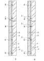
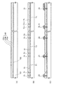
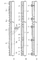
並置された複数の導波管と、壁面とで囲まれた処理室にヘリウムを含む反応性気体を供給する手段等を備えた製造装置において、ヘリウムを含む反応性気体を供給し、処理室内の圧力を大気圧若しくは準大気圧に保持しつつ、並置された導波管で挟まれた空間にマイクロ波を供給してプラズマを生成し、処理室内に載置された基板上に微結晶半導体でなる光電変換層を堆積する。並置された複数の導波管の対向する面にはスリットが設けられており、該スリットを介して処理室内にマイクロ波を供給しプラズマを生成することで、プラズマの高密度化を図ることができる。プラズマを生成するときの処理室の圧力は大気圧若しくは準大気圧とする。代表的には、1×10²Pa以上1×10⁵Pa以下(1Torr以上760Torr以下)の圧力が適用される。 In a manufacturing apparatus including a plurality of waveguides juxtaposed and a means for supplying a reactive gas containing helium to a processing chamber surrounded by a wall surface, the reactive gas containing helium is supplied, While maintaining the pressure at atmospheric pressure or quasi-atmospheric pressure, microwaves are supplied to the space between the juxtaposed waveguides to generate plasma, and a microcrystalline semiconductor is formed on the substrate placed in the processing chamber. A photoelectric conversion layer is deposited. Slits are provided on the opposing surfaces of the plurality of waveguides juxtaposed, and microwaves are supplied into the processing chamber through the slits to generate plasma, thereby increasing the plasma density. it can. The pressure in the processing chamber when generating plasma is atmospheric pressure or quasi-atmospheric pressure. Typically, a pressure of 1 × 10 2 Pa to 1 × 10 5 Pa (1 Torr to 760 Torr) is applied.
光電変換層は、一導電型の不純物が添加された不純物半導体層と、一導電型とは逆の導電型の不純物が添加された不純物半導体層との間に、真性な半導体層を有している。本発明は、光電変換層として、少なくとも真性な半導体層を微結晶半導体で形成する。また複数の導波管を並置して、これら導波管で挟まれた空間に高密度のプラズマを生成することができるため、本発明の半導体層を概略1×10²Pa以上1×10⁵Pa以下の圧力であっても安定して形成することができる。 The photoelectric conversion layer includes an intrinsic semiconductor layer between an impurity semiconductor layer to which an impurity of one conductivity type is added and an impurity semiconductor layer to which an impurity of a conductivity type opposite to the one conductivity type is added. Yes. In the present invention, at least an intrinsic semiconductor layer is formed of a microcrystalline semiconductor as a photoelectric conversion layer. In addition, since a plurality of waveguides can be juxtaposed and a high-density plasma can be generated in a space sandwiched between the waveguides, the semiconductor layer of the present invention is approximately 1 × 10 2 Pa or more and 1 × 10 5. It can be formed stably even at a pressure of Pa or less.
ここで、真性な半導体とは、該半導体に含まれる一導電型を付与する不純物(p型若しくはn型を付与する不純物)が1×1020cm−3以下の濃度であり、酸素及び窒素が9×1019cm−3以下の濃度であり、暗伝導度に対して光伝導度が100倍以上である半導体を指す。この真性半導体には、p型若しくはn型を付与する不純物、つまり周期表第13族若しくは第15族の不純物が含まれるものを含む。これは、微結晶半導体は、価電子制御を目的とした不純物を意図的に添加しないときであっても弱いn型の電気伝導性を示すので、真正な半導体層においては、p型を付与する不純物を成膜と同時に、或いは成膜後に、意図的若しくは非意図的に添加されることがあるためである。これを実質的に真性な半導体層といい、本発明の真性な半導体層に含まれ、これらを合わせて真性な半導体層(以下「i型半導体層」ともいう)と呼ぶ。
Here, an intrinsic semiconductor means that an impurity imparting one conductivity type (impurity imparting p-type or n-type) contained in the semiconductor has a concentration of 1 × 10 20 cm −3 or less, and oxygen and nitrogen are contained in the semiconductor. A semiconductor having a concentration of 9 × 10 19 cm −3 or less and a photoconductivity of 100 times or more with respect to dark conductivity. This intrinsic semiconductor includes an impurity imparting p-type or n-type, that is, an impurity containing a Group 13 or
本発明に係る微結晶半導体膜とは、非晶質半導体膜の中に結晶粒が分散するように存在する半導体膜である。このような微結晶半導体膜は多結晶半導体膜と異なり、微小な結晶構造又は結晶粒を半導体膜中に含ませつつ直接基板上に成膜することができる。具体的には、SiH4に対し、希釈ガスを用いて流量比で2〜1000倍、好ましくは10〜100倍に希釈し、マイクロ波帯の電磁エネルギーを供給してプラズマ化させ、ラジカル反応を誘起しつつ基板上に堆積する。希釈ガスには、水素、希ガス(ヘリウム、アルゴン、クリプトン、ネオン)、及びハロゲン気体(フッ素、塩素など)のいずれか一、又はこれらを組み合わせて用いることができ、さらに希ガスであるヘリウム、アルゴン、クリプトン、ネオンは複数組み合わせて用いることもできる。このように作製された微結晶半導体は、0.5nm〜20nmの結晶粒を非晶質半導体中に含んでいる。本発明では、このような半導体を少なくとも光電変換層に用いていれば良い。光電変換層は、その膜厚方向において全てが微結晶半導体若しくはそれに類する半導体である必要はなく、少なくとも膜厚方向における一部に微結晶半導体を含んでいれば良い。 The microcrystalline semiconductor film according to the present invention is a semiconductor film that exists so that crystal grains are dispersed in an amorphous semiconductor film. Unlike a polycrystalline semiconductor film, such a microcrystalline semiconductor film can be directly formed over a substrate while including a microcrystalline structure or crystal grains in the semiconductor film. Specifically, SiH 4 is diluted with a dilution gas in a flow rate ratio of 2 to 1000 times, preferably 10 to 100 times, and is converted into plasma by supplying electromagnetic energy in the microwave band, thereby causing radical reaction. Deposit on the substrate while inducing. As the dilution gas, any one of hydrogen, rare gas (helium, argon, krypton, neon), and halogen gas (fluorine, chlorine, etc.) or a combination thereof can be used. Argon, krypton, and neon can be used in combination. The microcrystalline semiconductor manufactured in this manner includes crystal grains of 0.5 nm to 20 nm in an amorphous semiconductor. In the present invention, such a semiconductor may be used at least for the photoelectric conversion layer. The photoelectric conversion layer does not necessarily have to be a microcrystalline semiconductor or a similar semiconductor in the film thickness direction, and it is sufficient that the photoelectric conversion layer includes at least a part of the microcrystalline semiconductor in the film thickness direction.
本発明によれば、微結晶半導体の成膜時の圧力を大気圧若しくは準大気圧として、マイクロ波プラズマを生成することにより、従来と比較して、50倍程度の堆積速度で形成することができ、良質な微結晶半導体を得ることができる。そのような微結晶半導体で光電変換層を形成することにより、光劣化による特性低下が5分の1から10分の1となり、実用上ほとんど問題のない光電変換装置を得ることができる。この光電変換装置の光電変換層の膜厚は0.5μm〜10μmであれば良いので、単結晶又は多結晶シリコンウエハを用いた光電変換装置と比べて資源を節約することができる。 According to the present invention, the pressure at the time of film formation of the microcrystalline semiconductor is set to atmospheric pressure or quasi-atmospheric pressure, and the microwave plasma is generated, so that the microcrystalline semiconductor can be formed at a deposition rate about 50 times that of the conventional case. And a high-quality microcrystalline semiconductor can be obtained. When a photoelectric conversion layer is formed using such a microcrystalline semiconductor, a characteristic deterioration due to light deterioration is reduced to 1/5 to 1/10, and a photoelectric conversion device having almost no problem in practical use can be obtained. Since the film thickness of the photoelectric conversion layer of this photoelectric conversion device may be 0.5 μm to 10 μm, resources can be saved as compared with a photoelectric conversion device using a single crystal or polycrystalline silicon wafer.
本発明の実施の形態について、図面を用いて以下に説明する。但し、本発明は以下の説明に限定されず、本発明の趣旨及びその範囲から逸脱することなくその形態及び詳細をさまざまに変更し得ることは当業者であれば容易に理解される。従って、本発明は以下に示す実施の形態の記載内容に限定して解釈されるものではない。以下に説明する本発明の構成において、同じものを指す符号は異なる図面間で共通して用いる。 Embodiments of the present invention will be described below with reference to the drawings. However, the present invention is not limited to the following description, and it will be easily understood by those skilled in the art that modes and details can be variously changed without departing from the spirit and scope of the present invention. Therefore, the present invention should not be construed as being limited to the description of the embodiments below. In the structure of the present invention described below, the same reference numerals are used in common in different drawings.
図1(A)は、本形態に係る光電変換装置の構成を示す。この光電変換装置は、p型半導体層14とn型半導体層18に挟まれてi型半導体層16を設けることにより、少なくとも一つの半導体接合を含んでいる。本実施の形態において、これらの層すべては、微結晶半導体層により構成される。
FIG. 1A illustrates a structure of a photoelectric conversion device according to this embodiment. This photoelectric conversion device includes at least one semiconductor junction by providing an i-
基板10は青板ガラス、白板ガラス、鉛ガラス、強化ガラス、セラミックガラスなど市販されている様々なガラス板を用いることができる。また、アルミノシリケート酸ガラス、バリウムホウケイ酸ガラスなどの無アルカリガラス基板と呼ばれるもの、石英基板、ステンレスなどの金属基板を用いることができる。基板10を光入射面とする場合には、第1電極12は酸化インジウム、酸化インジウム・スズ、酸化亜鉛などの透明導電膜材料で形成する。一方、第1電極12を反射電極とする場合にはアルミニウム、銀、チタン、タンタルなどの金属材料を用いて形成する。反射電極とする場合、電極の表面を凹凸化することにより、光を閉じこめることができ、光電変換装置の変換効率を向上させることができて好ましい。
As the
p型半導体層14は一導電型不純物として硼素を含む微結晶半導体で形成される。光吸収損失を低減させるためには、炭素を含ませて光学ギャップが広がるようにしても良い。
The p-
i型半導体層16は真性な半導体であって、微結晶半導体(代表的には微結晶シリコン)で形成される。なお、i型半導体は、該半導体に含まれるp型若しくはn型を付与する不純物が1×1020cm−3以下の濃度であり、酸素及び窒素が5×1019cm−3以下の濃度であり、暗伝導度に対して光伝導度が100倍以上である半導体である。特に酸素は1×1019cm−3以下、好ましくは5×1018cm−3以下とするとよい。酸素は微結晶半導体中でドナーとなるからである。このi型半導体層16は、0.1μm〜10μm、好ましくは0.5μm〜5μm、より好ましくは1μm〜3μmの厚さとする。
The i-
i型半導体層16には、p型を付与する不純物が1〜1000ppm添加されていてもよい。すなわち、微結晶半導体は、価電子制御を目的とした不純物を意図的に添加しないときに弱いn型の電気伝導性を示すので、i型半導体層16に適用する場合には、p型を付与する不純物を成膜と同時に、或いは成膜後に添加すると良い。p型を付与する不純物としては、代表的には硼素であり、B2H6、BF3などの不純物気体を1ppm〜1000ppmの割合で半導体材料ガスに混入させると良い。そしてボロンの濃度を、例えば1×10¹⁴〜6×1016cm−3とすると良い。
The i-
微結晶半導体は、非晶質と結晶構造(単結晶、多結晶を含む)の中間的な構造の半導体を含む。この半導体は、自由エネルギー的に安定な第3の状態を有する半導体であって、短距離秩序を持ち格子歪みを有する結晶質なものであり、その粒径を0.5〜20nmとして非単結晶半導体中に分散させて存在せしめることが可能である。また、未結合手(ダングリングボンド)を終端するものとして水素またはハロゲンを少なくとも1原子%またはそれ以上含んでいる。さらに、ヘリウム、アルゴン、クリプトン、ネオンなどの希ガスを含ませて格子歪みをさらに助長させることで安定性が増し良好な微結晶が得られる。このような微結晶シリコンは格子歪みを有し、該格子歪みにより光学特性が、単結晶シリコンの間接遷移型から直接遷移型に変化する。少なくとも10%の格子歪みがあれば、光学特性が直接遷移型に変化する。なお、歪みが局部的に存在することにより直接遷移と間接遷移とが混在した光学特性を呈することもできる。 A microcrystalline semiconductor includes a semiconductor having an intermediate structure between an amorphous structure and a crystalline structure (including a single crystal and a polycrystal). This semiconductor is a semiconductor having a third state which is stable in terms of free energy, and is a crystalline material having a short-range order and lattice strain, and having a grain size of 0.5 to 20 nm. It can be dispersed in a semiconductor. Further, it contains at least 1 atomic% or more of hydrogen or halogen as a terminal for dangling bonds (dangling bonds). Further, by adding a rare gas such as helium, argon, krypton, or neon to further promote lattice distortion, stability is improved and good microcrystals are obtained. Such microcrystalline silicon has lattice distortion, and the optical characteristics change from the indirect transition type to the direct transition type of single crystal silicon due to the lattice distortion. If there is at least 10% lattice distortion, the optical properties change directly to the transition type. In addition, since the distortion exists locally, an optical characteristic in which direct transition and indirect transition are mixed can be exhibited.
微結晶半導体はシランに代表される半導体材料ガスをマイクロ波帯の電磁エネルギーによりプラズマ化して、反応生成物を堆積させることにより形成される。代表的な半導体材料ガスとしては、SiH4であり、その他にもSi2H6、SiH2Cl2、SiHCl3、SiCl4、SiF4などを用いることができる。プラズマを生成する圧力は、大気圧若しくは準大気圧(1×10²Pa以上1×10⁵Pa以下)で行えば良い。このような圧力でプラズマを生成すると、気相中でラジカル反応が進み、被膜における表面反応と相まって成膜速度が向上する。この場合、マイクロ波を1kHz〜100kHzのパルス放電にすることで、気相反応は制御され気相中で粒子が生成されるなどの異常成長を抑えることができる。この半導体材料ガスを希釈ガスで希釈して用いることで大気圧若しくは準大気圧で生成されたプラズマを安定なものにすることができ、微結晶の形成を容易なものとすることができる。希釈ガスには、水素、希ガス(ヘリウム、アルゴン、クリプトン、ネオン)、及びハロゲン気体(フッ素、塩素など)のいずれか一、又はこれらを組み合わせて用いることができ、さらにヘリウム、アルゴン、クリプトン、ネオンも複数組み合わせすることができる。希釈率は10倍〜2000倍の範囲で半導体材料ガスを希釈することが好ましい。このような半導体材料ガスと希釈ガスとが含まれる反応性気体を用いて微結晶半導体を形成する。 A microcrystalline semiconductor is formed by depositing a reaction product by converting a semiconductor material gas typified by silane into plasma by electromagnetic energy in a microwave band. A typical semiconductor material gas is SiH 4 , and Si 2 H 6 , SiH 2 Cl 2 , SiHCl 3 , SiCl 4 , SiF 4, or the like can be used. The pressure for generating plasma may be atmospheric pressure or quasi-atmospheric pressure (1 × 10 2 Pa to 1 × 10 5 Pa). When plasma is generated at such a pressure, radical reaction proceeds in the gas phase, and the film formation rate is improved in combination with the surface reaction in the coating. In this case, by using a pulse discharge of 1 kHz to 100 kHz for the microwave, abnormal growth such as generation of particles in the gas phase can be suppressed by controlling the gas phase reaction. By diluting and using this semiconductor material gas with a diluent gas, plasma generated at atmospheric pressure or quasi-atmospheric pressure can be stabilized, and formation of microcrystals can be facilitated. As the dilution gas, any one of hydrogen, rare gas (helium, argon, krypton, neon), and halogen gas (fluorine, chlorine, etc.) or a combination thereof can be used. Further, helium, argon, krypton, A plurality of neons can be combined. It is preferable to dilute the semiconductor material gas in a dilution rate range of 10 to 2000 times. A microcrystalline semiconductor is formed using a reactive gas containing such a semiconductor material gas and a dilution gas.
プラズマを生成するためには1GHz〜5GHz、代表的には2.45GHzの電磁波を供給すれば良い。基板加熱温度は500℃以下が好ましく、100℃〜400℃の基板加熱温度が推奨される。また、半導体材料ガス中にCH4、C2H6などの炭素の水素化物、GeH4、GeF4などの水素化ゲルマニウム、フッ化ゲルマニウムを混合して、エネルギーバンド幅を1.5〜2.4eV、若しくは0.9〜1.1eVに調節しても良い。 In order to generate plasma, an electromagnetic wave of 1 GHz to 5 GHz, typically 2.45 GHz may be supplied. The substrate heating temperature is preferably 500 ° C. or lower, and a substrate heating temperature of 100 ° C. to 400 ° C. is recommended. Further, carbon hydride such as CH 4 and C 2 H 6 , germanium hydride such as GeH 4 and GeF 4 , and germanium fluoride are mixed in the semiconductor material gas, so that the energy bandwidth is 1.5-2. You may adjust to 4 eV or 0.9-1.1 eV.
n型半導体層18は一導電型不純物としてリンを含む微結晶半導体で形成される。微結晶半導体の代わりにアモルファス半導体で形成してもよい。n型半導体層18上の第2電極20はアルミニウム、銀、チタン、タンタル、クロムなどの金属材料を用いて形成する。なお、第2電極20側から光を入射させる場合には透明導電膜材料で形成する。
The n-
図1(A)は光電変換層の構成としてp型半導体層14、i型半導体層16、n型半導体層18を含むものを例示するが、光電変換層を構成する半導体接合としてはこのpin接合の他に他の構成を適用することもできる。
FIG. 1A illustrates a photoelectric conversion layer including a p-
図1(B)はp型半導体層14とi型半導体層16の間に、p−型半導体層15を設ける構成を示している。p−型半導体層15はp型半導体層14よりもp型を付与する不純物濃度が低い半導体層である。p−型半導体層15がp型半導体層14とi型半導体層16の間に存在することにより半導体接合界面におけるキャリア輸送性が改善される。この場合、p−型半導体層15におけるp型不純物濃度は、p型半導体層14からi型半導体層16にかけて階段状に、又は連続的に減少するように分布させることでキャリア輸送性はさらに改善する。また、この構成により界面準位密度が低減し拡散電位が向上するので、光電変換装置の開放電圧が高くなる。
FIG. 1B shows a configuration in which a p −
図2(A)は、i型半導体層16とn型半導体層18の間にアモルファス半導体でなるi’型半導体層17を設ける構成を示す。i’型半導体層17はi型半導体層16と、結晶性を有していない点で異なっている。i’型半導体層17は、i型半導体層16で吸収されなかった光を吸収する層である(外光が基板10側から入射する構成の場合を示している)。i型半導体層16の光学ギャップが約1.4eVであるのに対し、i’型半導体層17の光学ギャップは1.6eV〜1.8eVである。すなわち、可視光域の吸収係数がi’型半導体層17の方が高いという特性がある。そのため、i型半導体層16で吸収されなかった光をi’型半導体層17で吸収することが可能である。i’型半導体層17の膜厚はi型半導体層16の膜厚に対して2分の1から10分の1であれば良い。i’型半導体層17の光生成キャリアのうち、ホールはp型半導体層14側に流れることとなるが、キャリア輸送性の高いi型半導体層16を通過することにより再結合損失を低減することができる。すなわち、本構成によれば、光電流を増加させることができる。
FIG. 2A shows a configuration in which an i′-
図2(B)は、p型半導体層14とi型半導体層16の間に、p−型半導体層15を設け、i型半導体層16とn型半導体層18の間にアモルファス半導体でなるi’型半導体層17を設ける構成を示す。本構成により界面準位密度が低減し拡散電位が向上するので、光電変換装置の開放電圧が高くなり、光電流を増加させることができる。
In FIG. 2B, a p −
このような光電変換装置において、半導体層はそれぞれの界面を大気に触れさせることなく連続的に形成することが好ましい。また、各半導体層には価電子制御を目的として微量の不純物が添加されることから、複数の処理室が備えられたマルチ・チャンバ構成のマイクロ波プラズマCVD装置を用いることが好ましい。特にマイクロ波プラズマCVD法によるものであって、電子密度が1×1011cm−3以上1×1013cm−3以下であり、電子温度が0.2eV以上2.0eV以下(より好ましくは0.5eV以上1.5eV以下)程度であるものを用いることが好ましい。電子密度が高く、電子温度が低いプラズマを利用するとプラズマダメージが少なく欠陥が少ないことから良質な微結晶半導体膜を形成することができる。以下に微結晶半導体膜を形成するのに適した装置の一例を示す。 In such a photoelectric conversion device, it is preferable that the semiconductor layers are continuously formed without exposing each interface to the atmosphere. In addition, since a small amount of impurities is added to each semiconductor layer for the purpose of valence electron control, it is preferable to use a microwave plasma CVD apparatus having a multi-chamber configuration provided with a plurality of processing chambers. In particular, it is based on the microwave plasma CVD method, and has an electron density of 1 × 10 11 cm −3 or more and 1 × 10 13 cm −3 or less, and an electron temperature of 0.2 eV or more and 2.0 eV or less (more preferably 0 It is preferable to use one that is about 5 eV or more and 1.5 eV or less. When a plasma with a high electron density and a low electron temperature is used, a high-quality microcrystalline semiconductor film can be formed because there are few plasma damages and few defects. An example of an apparatus suitable for forming a microcrystalline semiconductor film is described below.
図3は複数の処理室を備えたマルチ・チャンバ・マイクロ波プラズマCVD装置の一例を示す。この装置は共通室306の周りに、ロード/アンロード室301、第1処理室302、第2処理室303、第3処理室304を備えた構成となっている。第1乃至第3の処理室302〜304は、上面を複数の導波管で、側面及び底面を壁面で囲まれた構成となっている。第1処理室302はp型半導体層を成膜し、第2処理室303はi型半導体層を成膜し、第3処理室304はn型半導体層を成膜する処理室である。
FIG. 3 shows an example of a multi-chamber microwave plasma CVD apparatus provided with a plurality of processing chambers. This apparatus includes a load / unload
被処理基板は共通室306を介して各処理室に搬出入される。共通室306と各室の間にはゲートバルブ307が備えられ、各処理室で行われる処理が、相互に干渉しないように構成されている。基板はロード/アンロード室301のカセット308に装填され、共通室306の搬送手段309により第1処理室302、第2処理室303、第3処理室304へ運ばれる。
The substrate to be processed is carried into and out of each processing chamber via the
各処理室内は不活性ガス又は窒素ガスで置換され、概略1×10²Pa以上1×10⁵Pa以下の圧力で処理用ガスを流すことができるように、ガス供給手段312、排気手段310が接続されている。本装置による成膜は上記圧力で行われるので、排気手段310は吸引排気能力が高いものが好ましい。排気手段310と各処理室との間には開閉バルブ311が設けられており、これによって排気速度を制御することもできる。
Each processing chamber is replaced with an inert gas or nitrogen gas, and the gas supply means 312 and the exhaust means 310 are provided so that the processing gas can flow at a pressure of approximately 1 × 10 2 Pa to 1 × 10 5 Pa. It is connected. Since the film formation by this apparatus is performed at the above pressure, the exhaust means 310 preferably has a high suction exhaust capability. An open /
ガス供給手段312は、シリンダ313、バルブ314、流量制御機器315などで構成されている。シリンダ313は、半導体材料ガス若しくは希ガスなどプロセスに用いるガス等が充填されている。希ガスとしてヘリウムを用いた場合、プラズマを安定に発生させることができる。ガス供給手段312pは第1処理室302に接続され、p型半導体層用のガスを供給する。ガス供給手段312iは第2処理室303に接続され、i型半導体層用のガスを供給する。ガス供給手段312nは第3処理室304に接続され、n型半導体層用のガスを供給する。ガス供給手段312hは水素を供給し、ガス供給手段312fは処理室内のクリーニングに用いるエッチングガスを供給する系統であり、これらは各処理室共通のラインとして構成されている。
The gas supply means 312 includes a
各処理室にはプラズマ発生手段305が設けられている。プラズマ発生手段305は処理室内でプラズマを発生させる発振器が含まれる。例えば、マイクロ波電源、マイクロ波増幅器とマイクロ波を処理室まで誘導する導波管などで構成される。プラズマ発生手段305は各処理室において一又は複数設けられている。プラズマ発生手段305は、被処理基板の面積に対して成膜される被膜の均一性を維持するために必要な数だけ設ければ良い。 Each processing chamber is provided with plasma generating means 305. The plasma generating means 305 includes an oscillator that generates plasma in the processing chamber. For example, it includes a microwave power source, a microwave amplifier, and a waveguide that guides the microwave to the processing chamber. One or a plurality of plasma generating means 305 are provided in each processing chamber. The number of plasma generation means 305 may be provided as many as necessary to maintain the uniformity of the film formed on the area of the substrate to be processed.
図4は処理室の一例を説明する断面図である。処理室は蓋体317と処理容器316とからなる。処理容器316は壁面を有しており、蓋体317は櫛歯状に並置された複数の導波管321を有している。処理容器316と、蓋体317との密閉構造により圧力を概略1×10²Pa以上1×10⁵Pa以下に保持できる。処理容器316は、例えば、ステンレス鋼、アルミニウムなどの金属で形成されている。
FIG. 4 is a cross-sectional view illustrating an example of a processing chamber. The processing chamber includes a
蓋体317と処理容器316で密閉空間が形成される処理室内は不活性ガス又は窒素ガスで置換可能となるようにガス供給手段312が設けられている。この処理室に接続される排気手段310は処理室に供給したガスを排出するためのものである。処理室内の雰囲気置換をより確実なものとするために、排気手段310は真空ポンプで構成しても良い。
A gas supply means 312 is provided in the processing chamber in which a sealed space is formed by the
処理容器316の内部には基板など被処理体を載置するサセプタ318が設けられている。サセプタ318は窒化アルミニウム、窒化シリコン、シリコンカーバイトなどのセラミックス材で構成されている。サセプタ318の内部には、ヒータ319が設けられている。ヒータ319はヒータ電源320に接続されている。ヒータ319はサセプタ318に埋め込まれており、ヒータ電源320から電力が供給されることにより発熱しサセプタ318に載置された基板を所定の温度に保持する。
A
蓋体317は処理容器316の上部を密閉する。蓋体317が有する導波管321は、処理室内で、櫛歯状に突出するように、複数が狭い間隔で並置されている。導波管は、2mm以上10mm以下の間隔で並置されている。導波管321は処理基板の一に対して複数が並置されている。このような導波管321はそれぞれマイクロ波電源322と連結されている。導波管321にはスリット323が設けられ、そこからマイクロ波が漏洩するようになっている。漏洩するとは、スリット323はマイクロ波を透過する誘電体板324で塞がれており、誘電体板324を介してマイクロ波が供給される状態を示す。誘電体板324は石英などから形成され、導波管321の中に処理用ガスが流れ込まないようにスリット323を塞いでいる。誘電体板324は、プラズマを均一に発生させるため、導波管321の中央に配置されている。スリット323の位置は、並置された導波管同士が対向する側に設けられている。つまり、スリット323同士は対向している。
The
ガス供給手段312は、処理用ガスが充填されたシリンダ313、バルブ314、流量制御機器315などで構成されている。流量制御機器315で流量が調整された処理用ガスは処理容器316内に供給される。シリンダ313は微結晶半導体の成膜に必要な処理用ガスが充填されている。成膜に必要な処理用ガスとしては、シラン若しくはジシランなどの半導体材料ガスや希釈ガス(水素若しくはフッ素、ヘリウム若しくはアルゴンなどの希ガス)、などが含まれる。処理容器316にはガスノズル325、ガスノズル326があり、当該ノズルから処理用ガスが処理容器316内に流れ出す構成となっている。例えば、ガスノズル325には水素若しくはフッ素、又はヘリウム若しくはアルゴンなどの希ガスを供給し、マイクロ波が供給される誘電体板324の近傍で高密度のラジカルを生成させ、被処理基板上で微結晶半導体の成長表面において表面反応を促進させる。ガスノズル326にはシラン若しくはジシランなどの半導体材料ガスを供給する。このように、ガスの供給経路を分離することで、誘電体板324への被膜の堆積を抑えることができる。成膜の段階では、ガスノズル325から水素若しくはフッ素、又はヘリウム若しくはアルゴンなどの希ガスを供給し続けても良い。
The gas supply means 312 includes a
マイクロ波は誘電体板324を通して処理室内に供給される。導波管321を並置してスリット323を対向する面に設けることにより、導波管321で挟まれた空間に高密度のプラズマを生成することができる。例えば、誘電体板324の表面を伝搬する表面波を利用して表面波プラズマを形成すると、無電磁場マイクロ波放電で、高密度で均一なプラズマを形成することができる。この場合、導波管321で挟まれた狭い空間、つまり狭い間隔にプラズマを形成するので、概略1×10²Pa以上1×10⁵Pa以下の圧力であっても安定してプラズマを形成することができる。導波管の間隔は2mm以上10mm以下の範囲で、上記圧力が高いほど狭く、上記圧力が低いほど広くすることができる。
The microwave is supplied into the processing chamber through the
導波管321で挟まれた空間には、並置された導波管321の間隔よりも広い間隔となるようにプラズマ発生器327が設けられている。プラズマ発生器327は、導波管321で挟まれた空間に、導波管321に沿って複数備えられている。プラズマ発生器327は、導波管321に接続されるものとは別のマイクロ波電源328に接続されている。マイクロ波電源328とプラズマ発生器327の間には電力増幅器329が設けられている。プラズマ発生器327は、導波管321へマイクロ波電力を投入して放電を開始するときに動作させ、プラズマ生成のきっかけをつくるために用いる。
A
プラズマ発生器327にはプラズマの状態を診断するプラズマモニタ機能が備えられており、その出力値が電力増幅器329に入力される。プラズマの状態を診断する方法としては、例えばラングミュアプローブなどが用いられ、電子密度や電子温度などを検出する。制御回路330には、処理室に設置された複数のプラズマ発生器327によりモニタされたプラズマの測定値が入力され、その値から処理室内のプラズマの密度が均一になるように、電力増幅器329のそれぞれに、増幅率を変える個別の制御信号を出力する。プラズマのジャンピング現象と呼ばれ、プラズマの高密度領域が放電空間内を遊動する現象を抑制するために有効である。
The
上記マイクロ波プラズマCVD装置は、導波管を複数に分割して並置することで、基板サイズの大型化に対しても均一なプラズマを生成することができる。基板サイズとしては、液晶ガラスで第1世代と呼ばれる300mm×400mmから、第3世代の550mm×650mm、第4世代の730mm×920mm、第5世代の1000mm×1200mm、第6世代の2450mm×1850mm、第7世代の1870mm×2200mm、第8世代の2000mm×2400mmなどで代表される各種の基板サイズに柔軟に対応することができる。 The microwave plasma CVD apparatus can generate uniform plasma even when the substrate size is increased by dividing the waveguide into a plurality of parts and juxtaposing the waveguides. As the substrate size, from 300 mm × 400 mm called the first generation in the liquid crystal glass, the third generation 550 mm × 650 mm, the fourth generation 730 mm × 920 mm, the fifth generation 1000 mm × 1200 mm, the sixth generation 2450 mm × 1850 mm, Various substrate sizes typified by the seventh generation 1870 mm × 2200 mm and the eighth generation 2000 mm × 2400 mm can be flexibly supported.
図5はこのような処理室の蓋体317と導波管321の構成を示す斜視図である。
導波管が並置されることにより、これらに挟まれた細溝状の空間が形成されている。並置される導波管321の対向する面にスリット323を塞ぐ誘電体板324が設けられ、そこからマイクロ波が漏洩してプラズマを生成する。プラズマ発生器327は、並置される導波管321の細溝状の空間に沿って複数設けられている。
FIG. 5 is a perspective view showing the configuration of the
By arranging the waveguides in parallel, a narrow groove-like space is formed between them. A
図6は蓋体317の構成を示す平面図である。導波管321は複数が並置され、互いに平行に延びている。導波管321にはスリット323が設けられ、そこからマイクロ波が漏洩するようになっている。スリット323の位置は、並置される導波管321が対向する側に設けられている。スリット323は、導波管321の中に処理用ガスが流れ込まないように、マイクロ波を透過する誘電体板324で塞がれている。被処理基板の面積が大きい場合であっても、複数の導波管321を並置させ、その挟まれた空間にマイクロ波放電を生成することで、プラズマ密度の均一化を図ることができる。さらに、当該空間に、マイクロ波電源328から電力が供給されるプラズマ発生器327を複数設け、電力増幅器329及び制御回路330によりプラズマ発生器327を制御してプラズマの安定化を図ることにより、プラズマ密度の均一化を図ることができる。このような構成により、例えば、730mm×920mmのガラス基板、若しくは一辺が1mを超えるサイズのガラス基板に対して処理を行うことができる。
FIG. 6 is a plan view showing the configuration of the
図7はプラズマ発生器327の構成を示す。石英等でなるガスノズル331はガス供給手段312に接続されている。ガスノズル331の外側にはマイクロ波電力が供給される放電用電極332が設けられている。ガスノズル331にはヘリウムなど放電開始電圧の低い非堆積性ガスが供給され、放電用電極332に電力が印加されることにより無電極放電が行われる。ガスノズル331の中で生成したプラズマは、ノズルの外側まで拡散する。このプラズマ発生器327を処理室に設けることで、ここで生成されたプラズマが放電開始のきっかけとなる。プローブ333はプラズマ診断用に用意されているものであり、例えば、ラングミュアプローブが適用される。このモニタ値は、電力増幅器329を介して制御回路330に入力される。
FIG. 7 shows the configuration of the
図8は複数の処理室を備えたインライン型のマルチ・チャンバ・マイクロ波プラズマCVD装置の一例を示す。第1処理室302、第2処理室303及び第3処理室304を直列に接続した構成を有し、第1処理室302と第3処理室304とにはロード/アンロード室301が設けられている。各処理室の間はゲートバルブ307で仕切られている。第1処理室302はp型半導体層を成膜し、第2処理室303はi型半導体層を成膜し、第3処理室304はn型半導体層を成膜する処理室である。
FIG. 8 shows an example of an in-line type multi-chamber microwave plasma CVD apparatus having a plurality of processing chambers. The
各処理室内は不活性ガス又は窒素ガスで置換され、概略1×10²Pa以上1×10⁵Pa以下の圧力で処理用ガスを流すことができるように、ガス供給手段312と排気手段310が接続されている。本装置による成膜は上記圧力で行われるので、排気手段310は吸引排気能力が高いものが好ましい。排気手段310と各処理室との間には開閉バルブ311が設けられており、これによって排気速度を制御することもできる。
Each processing chamber is replaced with an inert gas or nitrogen gas, and the gas supply means 312 and the exhaust means 310 are provided so that the processing gas can flow at a pressure of approximately 1 × 10 2 Pa to 1 × 10 5 Pa. It is connected. Since the film formation by this apparatus is performed at the above pressure, the exhaust means 310 preferably has a high suction exhaust capability. An open /
ガス供給手段312は、半導体材料ガス若しくは希釈ガスなどの処理用ガスが充填されるシリンダ313、バルブ314、流量制御機器315などで構成されている。ガス供給手段312pは第1処理室302に接続され、p型半導体層用のガスを供給する。ガス供給手段312iは第2処理室303に接続され、i型半導体層用のガスを供給する。ガス供給手段312nは第3処理室304に接続され、n型半導体層用のガスを供給する。ガス供給手段312hは水素を供給し、ガス供給手段312fは処理室内のクリーニングに用いるエッチングガスを供給する系統であり、これらは各処理室共通のラインとして構成されている。
The gas supply means 312 includes a
各処理室にはプラズマ発生手段305が設けられている。プラズマ発生手段305は処理室内でプラズマを発生させる発振器が含まれる。例えば、マイクロ波電源、マイクロ波増幅器とマイクロ波を処理室まで誘導する導波管などで構成される。プラズマ発生手段305は各処理室において一又は複数設けられている。プラズマ発生手段305は、被処理基板の面積に対して成膜される被膜の均一性を維持するために必要な数だけ設ければ良い。 Each processing chamber is provided with plasma generating means 305. The plasma generating means 305 includes an oscillator that generates plasma in the processing chamber. For example, it includes a microwave power source, a microwave amplifier, and a waveguide that guides the microwave to the processing chamber. One or a plurality of plasma generating means 305 are provided in each processing chamber. The number of plasma generation means 305 may be provided as many as necessary to maintain the uniformity of the film formed on the area of the substrate to be processed.
図8の構成のインライン型のマルチ・チャンバ・マイクロ波プラズマCVD装置によれば、複数の被処理基板を連続的に処理することができる。 According to the in-line type multi-chamber microwave plasma CVD apparatus having the configuration shown in FIG. 8, a plurality of substrates to be processed can be continuously processed.
このような構成のプラズマCVD装置によって、基板が載置された処理室内に処理用ガス(反応性気体)を供給し、基板と対向配置された導波管に設けられたスリットを介して処理室内にマイクロ波を供給する。そしてプラズマが生成され、基板上に微結晶半導体でなる半導体層を形成することができる。 With the plasma CVD apparatus having such a configuration, a processing gas (reactive gas) is supplied into the processing chamber in which the substrate is placed, and the processing chamber is inserted through a slit provided in a waveguide disposed to face the substrate. To supply microwaves. Then, plasma is generated and a semiconductor layer made of a microcrystalline semiconductor can be formed over the substrate.
上記構成のプラズマCVD装置を用いて微結晶半導体の成膜をする場合には、処理室内でプラズマを発生させるときにヘリウムを用いることが好ましい。つまりプラズマを発生させる電力を供給する前にヘリウムを供給すると好ましい。ヘリウムは24.5eVとすべての気体中で最も高いイオン化エネルギーを持つが、そのイオン化エネルギーよりも少し低い、約20eVの準位に準安定状態があるので、放電持続中においては、イオン化するエネルギーには、差分となる約4eVしか必要とせず、安定した放電が持続できる。また放電開始電圧も全ての気体中最も低い値を示す。このような特性から、大気圧若しくは準大気圧における放電で、ヘリウムはプラズマを安定的に維持することができる。また、均一なプラズマを形成することができるので、微結晶半導体層を堆積する基板の面積が大きくなっても均一な膜を堆積することができる。 In the case where a microcrystalline semiconductor film is formed using the plasma CVD apparatus having the above structure, helium is preferably used when generating plasma in the treatment chamber. That is, it is preferable to supply helium before supplying power for generating plasma. Helium has the highest ionization energy of all gases at 24.5 eV, but there is a metastable state at a level of about 20 eV, which is slightly lower than the ionization energy. Requires only about 4 eV as a difference, and stable discharge can be sustained. Moreover, the discharge start voltage also shows the lowest value among all gases. From such characteristics, helium can stably maintain the plasma by discharge at atmospheric pressure or sub-atmospheric pressure. In addition, since uniform plasma can be formed, a uniform film can be deposited even when the area of the substrate on which the microcrystalline semiconductor layer is deposited is increased.
半導体層でなる光電変換層の構成としてpin接合を形成する場合には、それぞれの微結晶半導体層に対応した処理室をマイクロ波プラズマCVD装置に設けることが好ましい。この場合、まず、被処理基板(第1の電極が形成された基板となる)が載置される第1処理室302に第1の処理用ガス(反応性気体)を供給し、基板と対向配置された導波管に設けられたスリットを介して第1処理室302内にマイクロ波を供給する。そしてプラズマが生成され、基板上に第1の微結晶半導体層(p型半導体層)が形成される。次いで、その基板を大気に晒すことなく第1処理室302から搬出し、第2処理室303へ移動させ、該基板が載置される第2処理室303に第2の処理用ガス(反応性気体)を供給し、同様にマイクロ波を供給してプラズマを生成し、第1の微結晶半導体層上に第2の微結晶半導体層(i型半導体層)を形成する。そして、その基板を大気に晒すことなく第2処理室303から搬出し、第3処理室304へ移動させ、該基板が載置される第3処理室304に第3の処理用ガス(反応性気体)を供給し、同様にマイクロ波を供給してプラズマを生成し、第2の微結晶半導体層上に第3の微結晶半導体層(n型半導体層)を形成する。
In the case where a pin junction is formed as a structure of the photoelectric conversion layer formed using a semiconductor layer, it is preferable to provide a treatment chamber corresponding to each microcrystalline semiconductor layer in the microwave plasma CVD apparatus. In this case, first, the first processing gas (reactive gas) is supplied to the
また、他の方法として、処理室内でp型半導体層、i型半導体層及びn型半導体層を連続して成膜しても良い。この場合、i型半導体層にp型不純物が取り込まれる量を低減するために、p型半導体層とi型半導体層の間で放電を止めて、シラン等に代表される反応性の高いガスを流して処理室内の雰囲気を置換しても良い。処理室内の残留物を除去するために、半導体層の成膜毎に処理室内のクリーニングをすることが好ましい。処理室内は下記のプラズマクリーニングをすることが好ましい。プラズマクリーニングの後は、シラン等に代表される反応性の高いガスを流して処理室内の残留不純物を除去しても良い。 As another method, a p-type semiconductor layer, an i-type semiconductor layer, and an n-type semiconductor layer may be successively formed in a treatment chamber. In this case, in order to reduce the amount of p-type impurities taken into the i-type semiconductor layer, the discharge is stopped between the p-type semiconductor layer and the i-type semiconductor layer, and a highly reactive gas typified by silane or the like is used. The atmosphere in the processing chamber may be replaced by flowing. In order to remove residues in the processing chamber, it is preferable to clean the processing chamber every time the semiconductor layer is formed. It is preferable to perform the following plasma cleaning in the processing chamber. After the plasma cleaning, a highly reactive gas typified by silane or the like may be flowed to remove residual impurities in the processing chamber.
半導体層を成膜する処理室は、エッチングガスを供給してプラズマクリーニングが行われる。エッチングガスとしては、三フッ化窒素(NF3)、六フッ化硫黄(SF6)などを用いることができる。エッチング後は、処理室内に残留するフッ素などの残留成分の影響を低減するために、処理室内をシリコンの被膜で被覆することが好ましい。このシリコンの被膜は、処理室内にシランを供給してプラズマを発生させて被覆させる。なお、不純物を有する半導体層を形成する処理室では、不純物を有する半導体の被膜で処理室内を被覆しても良い。例えば、p型半導体層を成膜する処理室ではp型半導体の被膜で被覆すればよい。このようにしてプラズマクリーニング後に処理室内をシリコン等の被膜で被覆することで、壁面からの脱ガスを低減させることができる。また、シランを供給してプラズマを生成したことにより、処理室内に残留する酸素、水分などはシランと反応して、処理室外へ真空排気されるので、処理室内の清浄度を高めることができる。同様に、半導体層の各層の成膜を開始する前に、シランを処理室内に流すことで、処理室内の清浄度を高めることができる。 A processing chamber in which the semiconductor layer is formed is supplied with an etching gas to perform plasma cleaning. As an etching gas, nitrogen trifluoride (NF 3 ), sulfur hexafluoride (SF 6 ), or the like can be used. After the etching, the processing chamber is preferably covered with a silicon film in order to reduce the influence of residual components such as fluorine remaining in the processing chamber. This silicon film is formed by supplying silane into the processing chamber to generate plasma. Note that in the treatment chamber in which the semiconductor layer having impurities is formed, the treatment chamber may be covered with a semiconductor film having impurities. For example, a processing chamber for forming a p-type semiconductor layer may be covered with a p-type semiconductor film. In this manner, after the plasma cleaning, the processing chamber is covered with a film such as silicon, so that degassing from the wall surface can be reduced. In addition, by supplying silane and generating plasma, oxygen, moisture, and the like remaining in the processing chamber react with silane and are evacuated to the outside of the processing chamber, so that the cleanliness of the processing chamber can be increased. Similarly, the cleanliness of the processing chamber can be increased by flowing silane into the processing chamber before starting the deposition of each layer of the semiconductor layer.
なお、処理室の数は積層する層の数に応じて設ければ良い。例えば、図1(B)のように、p型半導体層14とi型半導体層16の間に、p−型半導体層15を設ける場合には、新たな処理室を追加しても良い。p−型半導体層15を成膜する場合には、処理用ガスとして、シランと共に供給するジボランの濃度を概略1ppm未満の濃度に制御すれば良いが、他の方法としてセルフドーピングを利用しても良い。セルフドーピングとは、処理室内をp型の不純物を有する半導体で被覆しておくことにより、微量のp型不純物(硼素など)が成膜中に取り込まれ、p−型半導体層15の形成を可能とする方法である。
Note that the number of treatment chambers may be provided in accordance with the number of layers to be stacked. For example, when the p −
微結晶半導体層は、シラン(不純物を有する微結晶半導体層とする場合には、シランに加えドーピングガスを用いる)と、希釈ガスである水素及び/又は希ガスとを混合して高密度プラズマにより成膜する。シランは水素及び/又は希ガスで10倍から2000倍に希釈される。そのため多量の水素及び/又は希ガスが必要とされるため、微結晶半導体の成膜時に供給したガスは回収して再利用するとよい。図9はプラズマCVD装置に適用するガス精製循環装置334の一例を示す。
The microcrystalline semiconductor layer is formed by mixing silane (in the case of a microcrystalline semiconductor layer having impurities, a doping gas is used in addition to silane) with hydrogen and / or a rare gas as a diluent gas, and by high-density plasma. Form a film. Silane is diluted 10 to 2000 times with hydrogen and / or a noble gas. Therefore, since a large amount of hydrogen and / or a rare gas is required, the gas supplied at the time of forming the microcrystalline semiconductor may be recovered and reused. FIG. 9 shows an example of a
ガス精製循環装置334としては、シランなどの半導体材料ガスを回収精製するもの、ヘリウムなどの希ガスを回収精製するものがある。第2処理室303の処理用ガスはサーキュレータ(循環機)等で構成される排気手段310で吸引され、排気手段310から使用済みガスとして排出される。使用済みガスはフィルタ335により微粒子が除去されて回収ガス容器336に蓄積される。回収ガス容器336に蓄積された後は、昇圧器337により昇圧され、分離器338によりヘリウムなどの希ガスのみを分離する。分離器338の構成としては、膜分離、吸着分離、吸収分離、深冷分離方式などが適用される。分離精製されたガスは充填容器339に蓄積される。充填容器339に蓄積されたガスは、圧力調整器340で所定の圧力に調整され、ガス供給手段312の流量制御機器315の上流側に供給される。このようにして処理用ガスを再利用することで、微結晶半導体に必要な処理用ガスの消費量を削減することができる。すなわち、ヘリウムなどの希ガス等を再利用することにより、光電変換装置の製造に係る全エネルギー消費量を低減することができ、二酸化炭素の排出量を削減することができる。
Examples of the gas refining / circulating
このような装置を用いて形成される微結晶半導体膜は、大面積基板に均質に堆積することが可能であり、基板上において複数のユニットセルを直列に電気的接続された集積型光電変換装置を構成することが可能である。以下、その工程の概略について説明する。 The microcrystalline semiconductor film formed using such an apparatus can be uniformly deposited on a large-area substrate, and an integrated photoelectric conversion device in which a plurality of unit cells are electrically connected in series on the substrate Can be configured. The outline of the process will be described below.
図10と図11は、絶縁表面を有する基板上に複数の光電変換ユニットセルを設け、各光電変換ユニットセルが基板上で直列に接続された光電変換装置の製造工程を示す。基板10に第1電極12を形成する。第1電極12は開口M0〜Mnによって複数に絶縁分離されている(図10(A))。開口M0〜Mnは、基板10に導電膜を一面に形成しておき、その導電膜を開口パターンに合わせてエッチング除去、又はレーザ光等のエネルギービームによって直接的に加工して形成する。レーザ加工により基板10に形成された導電膜、半導体膜及び絶縁膜を加工する場合には、レーザ光を光学系にて集光して行うことが好ましい。微細な加工を可能とするためである。また上述のように大面積基板を効率良く加工するには、レーザ光を線状に集光して長尺の開口パターンを1回又は複数回のパルスレーザ光の照射により行うことが効率的である。
10 and 11 show a manufacturing process of a photoelectric conversion device in which a plurality of photoelectric conversion unit cells are provided on a substrate having an insulating surface, and each photoelectric conversion unit cell is connected in series on the substrate. The
第1電極12に開口M0〜Mnを形成した後、光電変換層となる半導体層を形成する。図10(A)では、第1電極12側からp型半導体層14、i型半導体層16、n型半導体層18を形成する場合を例示している。光電変換層の構成は、この構成に代えて図1及び図2で示す構成を適用することができる。光電変換層は、図3で示す複数の処理室を備えたマルチ・チャンバ・マイクロ波プラズマCVD装置によって形成することが好ましい。この構成のプラズマCVD装置を用いれば光電変換層を大気に触れさせずに連続して形成することができる。
After forming the openings M 0 to M n in the
光電変換層に開口C1〜Cnを形成する(図10(B))。開口C1〜Cnはp型半導体層14、i型半導体層16、n型半導体層18を貫通する開口であり、第1電極12の表面若しくは側面が露出するように加工する。開口C1〜Cnは所定の間隔をもって、開口M0〜Mnに隣接するように形成する。この工程もレーザ加工により行うことができる。
Openings C 1 to C n are formed in the photoelectric conversion layer (FIG. 10B). The openings C 1 to C n are openings that penetrate the p-
第2電極20は開口S1〜Snによって分離されており、開口C1〜Cnによって第1電極12と電気的に接続する(図11(A))。開口S1〜Snは所定の間隔をもって、開口C1〜Cnに隣接するように形成する。この工程もレーザ加工により行うことができる。レーザ加工を行う場合には、第2電極20にクロムを用いると昇華性であるので選択加工が容易となる。
The
これにより、第1電極12と第2電極20の間に光電変換層を有するユニットセルが複数形成され、それぞれのユニットセルが隣接するものと直列に接続された集積型構造を得ることができる。
Thereby, a plurality of unit cells having photoelectric conversion layers are formed between the
第2電極20上に取出電極22を設け、保護膜24で被覆して、保護フィルム25を設けた構成を示す(図11(B))。保護フィルム25は3層構造となっており、EVA(エチレンビニルアセテート)26は加熱すると融解する接着剤の層である。アルミ箔27は防湿のための層であり外部から進入する水蒸気を遮断するためのものである。外皮フィルム28はポリエチレンテレフタレート(PET)などで形成される。以上により基板10に複数のユニットセルが接続された光電変換装置を得ることができる。
A configuration is shown in which the
次に、印刷法で絶縁パターン若しくは導電パターンを形成する光電変換装置の製造工程を図12と図13を参照して説明する。基板101上に透光性電極層102を設ける。或いは透光性電極層102を備えた基板を用意する(図12(A))。透光性電極層102は酸化インジウム・スズ合金(ITO)、酸化亜鉛(ZnO)、酸化スズ(SnO2)、ITO−ZnO合金などで40〜200nm(好適には50〜100nm)の厚さとする。透光性電極層102のシート抵抗は20〜200Ω/□程度とすれば良い。
Next, a manufacturing process of a photoelectric conversion device that forms an insulating pattern or a conductive pattern by a printing method will be described with reference to FIGS. A light-transmitting
また、透光性電極層102として導電性高分子(導電性ポリマーともいう)を含む導電性組成物を用いることができる。導電性組成物は、透光性電極層102として薄膜を形成する場合、薄膜におけるシート抵抗が10000Ω/□以下、波長550nmにおける透光率が70%以上であることが好ましい。また、含まれる導電性高分子の抵抗率が0.1Ω・cm以下であることが好ましい。導電性高分子としては、いわゆるπ電子共役系導電性高分子が用いることができる。例えば、ポリアニリン及びまたはその誘導体、ポリピロール及びまたはその誘導体、ポリチオフェン及びまたはその誘導体、これらの2種以上の共重合体などが適用可能である。
Alternatively, a conductive composition containing a conductive high molecule (also referred to as a conductive polymer) can be used as the light-transmitting
共役系導電性高分子の具体例としては、ポリピロ−ル、ポリ(3−メチルピロ−ル)、ポリ(3−ブチルピロ−ル)、ポリ(3−オクチルピロ−ル)、ポリ(3−デシルピロ−ル)、ポリ(3,4−ジメチルピロ−ル)、ポリ(3,4−ジブチルピロ−ル)、ポリ(3−ヒドロキシピロ−ル)、ポリ(3−メチル−4−ヒドロキシピロ−ル)、ポリ(3−メトキシピロ−ル)、ポリ(3−エトキシピロ−ル)、ポリ(3−オクトキシピロ−ル)、ポリ(3−カルボキシルピロ−ル)、ポリ(3−メチル−4−カルボキシルピロ−ル)、ポリ(N−メチルピロール)、ポリチオフェン、ポリ(3−メチルチオフェン)、ポリ(3−ブチルチオフェン)、ポリ(3−オクチルチオフェン)、ポリ(3−デシルチオフェン)、ポリ(3−ドデシルチオフェン)、ポリ(3−メトキシチオフェン)、ポリ(3−エトキシチオフェン)、ポリ(3−オクトキシチオフェン)、ポリ(3−カルボキシルチオフェン)、ポリ(3−メチル−4−カルボキシルチオフェン)、ポリ(3,4−エチレンジオキシチオフェン)、ポリアニリン、ポリ(2−メチルアニリン)、ポリ(2−オクチルアニリン)、ポリ(2−イソブチルアニリン)、ポリ(3−イソブチルアニリン)、ポリ(2−アニリンスルホン酸)、ポリ(3−アニリンスルホン酸)等が適用可能である。 Specific examples of the conjugated conductive polymer include polypyrrole, poly (3-methylpyrrole), poly (3-butylpyrrole), poly (3-octylpyrrole), and poly (3-decylpyrrole). ), Poly (3,4-dimethylpyrrole), poly (3,4-dibutylpyrrole), poly (3-hydroxypyrrole), poly (3-methyl-4-hydroxypyrrole), poly ( 3-methoxypyrrole), poly (3-ethoxypyrrole), poly (3-octoxypyrrole), poly (3-carboxylpyrrole), poly (3-methyl-4-carboxylpyrrole), poly (N-methylpyrrole), polythiophene, poly (3-methylthiophene), poly (3-butylthiophene), poly (3-octylthiophene), poly (3-decylthiophene), poly (3-dodecylthio) Phen), poly (3-methoxythiophene), poly (3-ethoxythiophene), poly (3-octoxythiophene), poly (3-carboxylthiophene), poly (3-methyl-4-carboxylthiophene), poly ( 3,4-ethylenedioxythiophene), polyaniline, poly (2-methylaniline), poly (2-octylaniline), poly (2-isobutylaniline), poly (3-isobutylaniline), poly (2-aniline sulfone) Acid), poly (3-anilinesulfonic acid) and the like are applicable.
上記導電性高分子を、単独で導電性組成物として透光性電極層に使用してもよいし、導電性組成物の性質を調整するために有機樹脂を添加して使用することができる。 The said conductive polymer may be used for a translucent electrode layer independently as a conductive composition, and in order to adjust the property of a conductive composition, an organic resin can be added and used.
有機樹脂としては、導電性高分子と相溶または混合分散可能であれば熱硬化性樹脂であってもよく、熱可塑性樹脂であってもよく、光硬化性樹脂であってもよい。例えば、ポリエチレンテレフタレ−ト、ポリブチレンテレフタレ−ト、ポリエチレンナフタレ−ト等のポリエステル系樹脂、ポリイミド、ポリアミド−イミド等のポリイミド系樹脂、ポリアミド6、ポリアミド6,6、ポリアミド12、ポリアミド11等のポリアミド樹脂、ポリフッ化ビニリデン、ポリフッ化ビニル、ポリテトラフルオロエチレン、エチレン−テトラフルオロエチレンコポリマ−、ポリクロロトリフルオロエチレン等のフッ素樹脂、ポリビニルアルコ−ル、ポリビニルエ−テル、ポリビニルブチラ−ル、ポリ酢酸ビニル、ポリ塩化ビニル等のビニル樹脂、エポキシ樹脂、キシレン樹脂、アラミド樹脂、ポリウレタン系樹脂、ポリウレア系樹脂、メラミン樹脂、フェノ−ル系樹脂、ポリエ−テル、アクリル系樹脂及びこれらの共重合体等が適用可能である。
The organic resin may be a thermosetting resin, may be a thermoplastic resin, or may be a photocurable resin as long as it is compatible or mixed and dispersed with the conductive polymer. For example, polyester resins such as polyethylene terephthalate, polybutylene terephthalate, polyethylene naphthalate, polyimide resins such as polyimide and polyamide-imide, polyamide 6, polyamide 6,6,
さらに、導電性組成物の電気伝導度を調整するために、導電性組成物にアクセプタ性またはドナ−性ド−パントをド−ピングすることにより、共役導電性高分子の共役電子の酸化還元電位を変化させてもよい。 Further, in order to adjust the electric conductivity of the conductive composition, an oxidation-reduction potential of a conjugated electron of the conjugated conductive polymer is obtained by doping an acceptor or donor dopant into the conductive composition. May be changed.
アクセプタ性ド−パントとしては、ハロゲン化合物、ルイス酸、プロトン酸、有機シアノ化合物、有機金属化合物等を使用することができる。ハロゲン化合物としては、塩素、臭素、ヨウ素、塩化ヨウ素、臭化ヨウ素、フッ化ヨウ素等が挙げられる。ルイス酸としては五フッ化燐、五フッ化ヒ素、五フッ化アンチモン、三フッ化硼素、三塩化硼素、三臭化硼素等が挙げられる。プロトン酸としては、塩酸、硫酸、硝酸、リン酸、ホウフッ化水素酸、フッ化水素酸、過塩素酸等の無機酸と、有機カルボン酸、有機スルホン酸等の有機酸を挙げることができる。有機カルボン酸及び有機スルホン酸としては、前記カルボン酸化合物及びスルホン酸化合物を使用することができる。有機シアノ化合物としては、共役結合に二つ以上のシアノ基を含む化合物が使用できる。例えば、テトラシアノエチレン、テトラシアノエチレンオキサイド、テトラシアノベンゼン、テトラシアノキノジメタン、テトラシアノアザナフタレン等が適用可能である。 As the acceptor dopant, a halogen compound, a Lewis acid, a proton acid, an organic cyano compound, an organometallic compound, or the like can be used. Examples of the halogen compound include chlorine, bromine, iodine, iodine chloride, iodine bromide, and iodine fluoride. Examples of the Lewis acid include phosphorus pentafluoride, arsenic pentafluoride, antimony pentafluoride, boron trifluoride, boron trichloride, boron tribromide and the like. Examples of the protic acid include inorganic acids such as hydrochloric acid, sulfuric acid, nitric acid, phosphoric acid, borohydrofluoric acid, hydrofluoric acid, and perchloric acid, and organic acids such as organic carboxylic acid and organic sulfonic acid. As the organic carboxylic acid and organic sulfonic acid, the carboxylic acid compound and sulfonic acid compound can be used. As the organic cyano compound, a compound containing two or more cyano groups in a conjugated bond can be used. For example, tetracyanoethylene, tetracyanoethylene oxide, tetracyanobenzene, tetracyanoquinodimethane, tetracyanoazanaphthalene, and the like are applicable.
ドナー性ドーパントとしては、アルカリ金属、アルカリ土類金属、3級アミン化合物等を適用することができる。 As the donor dopant, an alkali metal, an alkaline earth metal, a tertiary amine compound, or the like can be used.
導電性組成物を、水または有機溶剤(アルコール系溶剤、ケトン系溶剤、エステル系溶剤、炭化水素系溶剤、芳香族系溶剤など)に溶解させて、湿式法により透光性電極層となる薄膜を形成することができる。導電性組成物を溶解する溶媒としては、特に限定することはなく、上記した導電性高分子及び有機樹脂などの高分子樹脂化合物を溶解するものを用いればよく、例えば、水、メタノール、エタノール、プロピレンカーボネート、N‐メチルピロリドン、ジメチルホルムアミド、ジメチルアセトアミド、シクロヘキサノン、アセトン、メチルエチルケトン、メチルイソブチルケトン、トルエンなどの単独もしくは混合溶剤に溶解すればよい。 A thin film in which a conductive composition is dissolved in water or an organic solvent (alcohol solvent, ketone solvent, ester solvent, hydrocarbon solvent, aromatic solvent, etc.) to form a light-transmitting electrode layer by a wet method Can be formed. The solvent that dissolves the conductive composition is not particularly limited, and a solvent that dissolves a polymer resin compound such as the above-described conductive polymer and organic resin may be used. For example, water, methanol, ethanol, What is necessary is just to melt | dissolve in single or mixed solvents, such as propylene carbonate, N-methylpyrrolidone, dimethylformamide, dimethylacetamide, cyclohexanone, acetone, methyl ethyl ketone, methyl isobutyl ketone, toluene.
導電性組成物の成膜は上述のように溶媒に溶解した後、塗布法、コーティング法、液滴吐出法(インクジェット法ともいう)、印刷法等の湿式法を用いて成膜することができる。溶媒の乾燥は、熱処理を行ってもよいし、減圧下で行ってもよい。また、有機樹脂が熱硬化性の場合はさらに加熱処理を行い、光硬化性の場合は光照射処理を行えばよい。 The conductive composition can be formed by dissolving in a solvent as described above and then using a wet method such as a coating method, a coating method, a droplet discharge method (also referred to as an inkjet method), or a printing method. . The solvent may be dried by heat treatment or under reduced pressure. Further, when the organic resin is thermosetting, heat treatment may be further performed, and when the organic resin is photocurable, light irradiation treatment may be performed.
また、透光性電極層102として正孔輸送性有機化合物と、該正孔輸送性有機化合物に対し電子受容性を示す金属酸化物とを含む複合透光性導電材料を用いて形成することができる。この複合透光性導電材料は、正孔輸送性有機化合物と、該正孔輸送性有機化合物に対し電子受容性を示す金属酸化物とを複合化させることで、抵抗率を1×10⁶Ω・cm以下とすることができる。なお「複合」とは、単に2つの材料を混合させるだけでなく、混合することによって材料間での電荷の授受が行われ得る状態になることを言う。
Alternatively, the light-transmitting
複合透光性導電材料は、第1の有機化合物と無機化合物とを複合してなる複合材料である。複合透光性導電材料に用いる第1の有機化合物としては、芳香族アミン化合物、カルバゾール誘導体、芳香族炭化水素、高分子化合物(オリゴマー、デンドリマー、ポリマー等)など、種々の化合物を用いることができる。なお、複合材料に用いる第1の有機化合物としては、正孔輸送性の高い有機化合物であることが好ましい。具体的には、1×10⁻⁶cm2/Vsec以上の正孔移動度を有する物質であることが好ましい。但し、電子よりも正孔の輸送性の高い物質であれば、これら以外のものを用いてもよい。 The composite translucent conductive material is a composite material formed by combining a first organic compound and an inorganic compound. As the first organic compound used for the composite light-transmitting conductive material, various compounds such as aromatic amine compounds, carbazole derivatives, aromatic hydrocarbons, and high molecular compounds (oligomers, dendrimers, polymers, and the like) can be used. . Note that the first organic compound used for the composite material is preferably an organic compound having a high hole-transport property. Specifically, a substance having a hole mobility of 1 × 10 −6 cm 2 / Vsec or more is preferable. Note that other than these substances, any substance that has a property of transporting more holes than electrons may be used.
複合材料に用いることのできる第1の有機化合物としては以下に例示するものを適用することができる。芳香族アミン化合物としては、4,4’−ビス[N−(1−ナフチル)−N−フェニルアミノ]ビフェニル(略称:NPB)、4,4’−ビス[N−(3−メチルフェニル)−N−フェニルアミノ]ビフェニル(略称:TPD)、4,4’,4’’−トリス(N,N−ジフェニルアミノ)トリフェニルアミン(略称:TDATA)、4,4’,4’’−トリス[N−(3−メチルフェニル)−N−フェニルアミノ]トリフェニルアミン(略称:MTDATA)などを適用することができる。 As the first organic compound that can be used for the composite material, those exemplified below can be applied. As an aromatic amine compound, 4,4′-bis [N- (1-naphthyl) -N-phenylamino] biphenyl (abbreviation: NPB), 4,4′-bis [N- (3-methylphenyl)- N-phenylamino] biphenyl (abbreviation: TPD), 4,4 ′, 4 ″ -tris (N, N-diphenylamino) triphenylamine (abbreviation: TDATA), 4,4 ′, 4 ″ -tris [ N- (3-methylphenyl) -N-phenylamino] triphenylamine (abbreviation: MTDATA) or the like can be used.
また、以下に示す有機化合物を用いることにより、450nm〜800nmの波長領域において、吸収ピークを有しない複合材料を得ることができる。また、同時に抵抗率を1×10⁶Ω・cm以下、代表的には5×10⁴〜1×10⁶Ω・cmとすることができる。 In addition, by using the organic compound shown below, a composite material having no absorption peak can be obtained in a wavelength region of 450 nm to 800 nm. At the same time, the resistivity can be set to 1 × 10 6 Ω · cm or less, typically 5 × 10 4 to 1 × 10 6 Ω · cm.
450nm〜800nmの波長領域において、吸収ピークを有しない複合材料に含まれる芳香族アミンとしては、N,N’−ジ(p−トリル)−N,N’−ジフェニル−p−フェニレンジアミン(略称:DTDPPA)、4,4’−ビス[N−(4−ジフェニルアミノフェニル)−N−フェニルアミノ]ビフェニル(略称:DPAB)、4,4’−ビス(N−{4−[N−(3−メチルフェニル)−N−フェニルアミノ]フェニル}−N−フェニルアミノ)ビフェニル(略称:DNTPD)、1,3,5−トリス[N−(4−ジフェニルアミノフェニル)−N−フェニルアミノ]ベンゼン(略称:DPA3B)等を適用することができる。 As an aromatic amine contained in a composite material having no absorption peak in a wavelength region of 450 nm to 800 nm, N, N′-di (p-tolyl) -N, N′-diphenyl-p-phenylenediamine (abbreviation: DTDPPA), 4,4′-bis [N- (4-diphenylaminophenyl) -N-phenylamino] biphenyl (abbreviation: DPAB), 4,4′-bis (N- {4- [N- (3- Methylphenyl) -N-phenylamino] phenyl} -N-phenylamino) biphenyl (abbreviation: DNTPD), 1,3,5-tris [N- (4-diphenylaminophenyl) -N-phenylamino] benzene (abbreviation) : DPA3B) or the like can be applied.
また、450nm〜800nmの波長領域において、吸収ピークを有しない複合材料に用いることのできるカルバゾール誘導体としては、具体的には、3−[N−(9−フェニルカルバゾール−3−イル)−N−フェニルアミノ]−9−フェニルカルバゾール(略称:PCzPCA1)、3,6−ビス[N−(9−フェニルカルバゾール−3−イル)−N−フェニルアミノ]−9−フェニルカルバゾール(略称:PCzPCA2)、3−[N−(1−ナフチル)−N−(9−フェニルカルバゾール−3−イル)アミノ]−9−フェニルカルバゾール(略称:PCzPCN1)等を適用することができる。 As a carbazole derivative that can be used for a composite material having no absorption peak in the wavelength region of 450 nm to 800 nm, specifically, 3- [N- (9-phenylcarbazol-3-yl) -N— Phenylamino] -9-phenylcarbazole (abbreviation: PCzPCA1), 3,6-bis [N- (9-phenylcarbazol-3-yl) -N-phenylamino] -9-phenylcarbazole (abbreviation: PCzPCA2), 3 -[N- (1-naphthyl) -N- (9-phenylcarbazol-3-yl) amino] -9-phenylcarbazole (abbreviation: PCzPCN1) or the like can be used.
また、4,4’−ジ(N−カルバゾリル)ビフェニル(略称:CBP)、1,3,5−トリス[4−(N−カルバゾリル)フェニル]ベンゼン(略称:TCPB)、9−[4−(N−カルバゾリル)]フェニル−10−フェニルアントラセン(略称:CzPA)、2,3,5,6−トリフェニル−1,4−ビス[4−(N−カルバゾリル)フェニル]ベンゼン等を用いることができる。 In addition, 4,4′-di (N-carbazolyl) biphenyl (abbreviation: CBP), 1,3,5-tris [4- (N-carbazolyl) phenyl] benzene (abbreviation: TCPB), 9- [4- ( N-carbazolyl)] phenyl-10-phenylanthracene (abbreviation: CzPA), 2,3,5,6-triphenyl-1,4-bis [4- (N-carbazolyl) phenyl] benzene, and the like can be used. .
また、450nm〜800nmの波長領域において、吸収ピークを有しない複合材料に用いることのできる芳香族炭化水素としては、例えば、9,10−ジ(ナフタレン−2−イル)−2−tert−ブチルアントラセン(略称:t−BuDNA)、9,10−ジ(ナフタレン−1−イル)−2−tert−ブチルアントラセン、9,10−ビス(3,5−ジフェニルフェニル)アントラセン(略称:DPPA)、9,10−ジ(4−フェニルフェニル)−2−tert−ブチルアントラセン(略称:t−BuDBA)、9,10−ジ(ナフタレン−2−イル)アントラセン(略称:DNA)、9,10−ジフェニルアントラセン(略称:DPAnth)、2−tert−ブチルアントラセン(略称:t−BuAnth)、9,10−ジ(4−メチルナフタレン−1−イル)アントラセン(略称:DMNA)、2−tert−ブチル−9,10−ビス[2−(ナフタレン−1−イル)フェニル]アントラセン、9,10−ビス[2−(ナフタレン−1−イル)フェニル]アントラセン、2,3,6,7−テトラメチル−9,10−ジ(ナフタレン−1−イル)アントラセン、2,3,6,7−テトラメチル−9,10−ジ(ナフタレン−2−イル)アントラセン、9,9’−ビアントリル、10,10’−ジフェニル−9,9’−ビアントリル、10,10’−ジ(2−フェニルフェニル)−9,9’−ビアントリル、10,10’−ビス[(2,3,4,5,6−ペンタフェニル)フェニル]−9,9’−ビアントリル、アントラセン、テトラセン、ルブレン、ペリレン、2,5,8,11−テトラ(tert−ブチル)ペリレン等が挙げられる。また、この他、ペンタセン、コロネン等も用いることができる。このように、1×10−6cm2/Vsec以上の正孔移動度を有し、炭素数14〜42である芳香族炭化水素を用いることがより好ましい。 Moreover, as an aromatic hydrocarbon which can be used for a composite material having no absorption peak in a wavelength region of 450 nm to 800 nm, for example, 9,10-di (naphthalen-2-yl) -2-tert-butylanthracene (Abbreviation: t-BuDNA), 9,10-di (naphthalen-1-yl) -2-tert-butylanthracene, 9,10-bis (3,5-diphenylphenyl) anthracene (abbreviation: DPPA), 9, 10-di (4-phenylphenyl) -2-tert-butylanthracene (abbreviation: t-BuDBA), 9,10-di (naphthalen-2-yl) anthracene (abbreviation: DNA), 9,10-diphenylanthracene ( Abbreviation: DPAnth), 2-tert-butylanthracene (abbreviation: t-BuAnth), 9,10-di (4 Methylnaphthalen-1-yl) anthracene (abbreviation: DMNA), 2-tert-butyl-9,10-bis [2- (naphthalen-1-yl) phenyl] anthracene, 9,10-bis [2- (naphthalene- 1-yl) phenyl] anthracene, 2,3,6,7-tetramethyl-9,10-di (naphthalen-1-yl) anthracene, 2,3,6,7-tetramethyl-9,10-di ( Naphthalen-2-yl) anthracene, 9,9′-bianthryl, 10,10′-diphenyl-9,9′-bianthryl, 10,10′-di (2-phenylphenyl) -9,9′-bianthryl, 10 , 10′-bis [(2,3,4,5,6-pentaphenyl) phenyl] -9,9′-bianthryl, anthracene, tetracene, rubrene, perylene, 2,5,8,11 Tetra (tert- butyl) perylene, and the like. In addition, pentacene, coronene, and the like can also be used. Thus, it is more preferable to use an aromatic hydrocarbon having a hole mobility of 1 × 10 −6 cm 2 / Vsec or more and having 14 to 42 carbon atoms.
なお、450nm〜800nmの波長領域において、吸収ピークを有しない複合材料に用いることのできる芳香族炭化水素は、ビニル骨格を有していてもよい。ビニル骨格を有している芳香族炭化水素としては、例えば、4,4’−ビス(2,2−ジフェニルビニル)ビフェニル(略称:DPVBi)、9,10−ビス[4−(2,2−ジフェニルビニル)フェニル]アントラセン(略称:DPVPA)等を適用することができる。 Note that the aromatic hydrocarbon that can be used for the composite material having no absorption peak in the wavelength region of 450 nm to 800 nm may have a vinyl skeleton. As the aromatic hydrocarbon having a vinyl skeleton, for example, 4,4′-bis (2,2-diphenylvinyl) biphenyl (abbreviation: DPVBi), 9,10-bis [4- (2,2- Diphenylvinyl) phenyl] anthracene (abbreviation: DPVPA) or the like can be used.
また、ポリ{4−[N−(4−ジフェニルアミノフェニル)−N−フェニル]アミノスチレン}(略称:PStDPA)、ポリ{4−[N−(9−カルバゾール−3−イル)−N−フェニルアミノ]スチレン}(略称:PStPCA)、ポリ(N−ビニルカルバゾール)(略称:PVK)やポリ(4−ビニルトリフェニルアミン)(略称:PVTPA)等の高分子化合物を用いることもできる。 Further, poly {4- [N- (4-diphenylaminophenyl) -N-phenyl] aminostyrene} (abbreviation: PStDPA), poly {4- [N- (9-carbazol-3-yl) -N-phenyl Amino] styrene} (abbreviation: PStPCA), poly (N-vinylcarbazole) (abbreviation: PVK), and poly (4-vinyltriphenylamine) (abbreviation: PVTPA) can also be used.
また、複合材料に用いる無機化合物としては、遷移金属酸化物が好ましい。また周期表における第4族乃至第8族に属する金属の酸化物であることが好ましい。具体的には、酸化バナジウム、酸化ニオブ、酸化タンタル、酸化クロム、酸化モリブデン、酸化タングステン、酸化マンガン、酸化レニウムは電子受容性が高いため好ましい。中でも特に、酸化モリブデンは大気中でも安定であり、吸湿性が低く、扱いやすいので好ましい。 As the inorganic compound used for the composite material, a transition metal oxide is preferable. In addition, an oxide of a metal belonging to Groups 4 to 8 in the periodic table is preferable. Specifically, vanadium oxide, niobium oxide, tantalum oxide, chromium oxide, molybdenum oxide, tungsten oxide, manganese oxide, and rhenium oxide are preferable because of their high electron accepting properties. Among these, molybdenum oxide is especially preferable because it is stable in the air, has a low hygroscopic property, and is easy to handle.
なお、複合材料を含む層の製造方法は、湿式法、乾式法を問わず、どのような手法を用いても良い。例えば、複合材料を含む層は、上述した有機化合物と無機化合物との共蒸着で作製することができる。なお、酸化モリブデンは真空中で蒸発しやすいため、蒸着法により複合材料を含む層を作製する場合、作製プロセスの面から好ましい。また、上述した有機化合物と金属アルコキシドを含む溶液を塗布し、焼成することによって複合材料を含む層を作製することもできる。塗布する方法としては、インクジェット法、スピンコート法等を用いることができる。 Note that any method may be used for manufacturing the layer including the composite material regardless of a wet method or a dry method. For example, the layer including the composite material can be manufactured by co-evaporation of the organic compound and the inorganic compound described above. Note that molybdenum oxide is easy to evaporate in a vacuum, and thus, when a layer containing a composite material is manufactured by an evaporation method, it is preferable from the viewpoint of a manufacturing process. In addition, a layer containing a composite material can be manufactured by applying and baking a solution containing the above-described organic compound and metal alkoxide. As a coating method, an inkjet method, a spin coating method, or the like can be used.
複合材料に含まれる有機化合物の種類を選択することにより、450nm〜800nmの波長領域において、吸収ピークを有しない複合材料を得ることができる。よって、自発光型の発光装置に用いる場合、発光領域からの発光を吸収することなく効率良く透過し、外部取り出し効率を向上させることができる。また、バックライトからの光についても吸収することなく、効率良く透過するため、外部取り出し効率を向上させることができる。また、複合材料を含む層は、曲げに強い。つまり、可撓性を有する基板を用いて光電変換装置を作製する場合に好適に用いることができる。 By selecting the type of organic compound contained in the composite material, a composite material having no absorption peak in the wavelength region of 450 nm to 800 nm can be obtained. Therefore, when used in a self-luminous light-emitting device, light emitted from the light-emitting region can be efficiently transmitted without being absorbed, and external extraction efficiency can be improved. Further, since light from the backlight is transmitted efficiently without being absorbed, the external extraction efficiency can be improved. In addition, the layer including the composite material is resistant to bending. That is, it can be suitably used when a photoelectric conversion device is manufactured using a flexible substrate.
透光性電極層102はITO膜が適しているが、プラズマによるダメージを受けやすい。しかし、本形態に係るマイクロ波プラズマCVD法では、電子温度が低いので電極材料の劣化を抑制することができる。勿論、ITO膜の劣化を防ぐために、ITO膜上にSnO2膜やZnO膜を形成することは有効である。ガリウム(Ga)を1〜10wt%含むZnO(ZnO:Ga)膜は透過率が高くITO膜上に積層させるには好適な材料である。その組み合わせの一例として、ITO膜を50〜60nmの厚さに形成し、その上にZnO:Ga膜を25nm形成すると失透を防止することが可能であり、良好な光透過特性を得ることができる。この積層膜においてシート抵抗は120〜150Ω/□が得られる。
An ITO film is suitable for the
光電変換層103は前述のマイクロ波プラズマCVD法で作製される微結晶半導体で構成される。微結晶半導体の代表例としては、SiH4を原料として作製される微結晶シリコン半導体であり、その他に微結晶シリコン・ゲルマニウム半導体、微結晶シリコンカーバイト半導体が適用される。光電変換層103は半導体接合を含む。本形態に係るマイクロ波プラズマCVD法では、電子温度が低いので各接合界面でのダメージが抑制され、良好な半導体接合を有する光電変換層を形成することができる。
The
図12(A)では、光電変換層103が透光性電極層102側からp型半導体層103a、i型半導体層103b、n型半導体層103cが積層された状態を一例として示す。それぞれの層の厚さは、p型半導体層103aで10〜20nm、i型半導体層103bで0.1μm〜10μm、好ましくは0.5μm〜5μm、より好ましくは1μm〜3μm、n型半導体層103cで20〜60nmとすることができる。
FIG. 12A illustrates an example in which the
p型半導体層103a、i型半導体層103b、n型半導体層103cを積層した状態、又はi型半導体層103bまでを積層した段階で、これらの微結晶半導体層にレーザ光を照射して結晶性を向上させる処理を行っても良い。微結晶半導体層に照射するレーザ光は、紫外光、可視光、又は赤外光を用いることができる。紫外光、可視光、又は赤外光を発振することが可能なレーザ発振器としては、KrF、ArF、XeCl、Xe等のエキシマレーザ発振器、He、He−Cd、Ar、He−Ne、HF等の気体レーザ発振器、YAG、GdVO4、YVO4、YLF、YAlO3などの結晶にCr、Nd、Er、Ho、Ce、Co、Ti又はTmをドープした結晶を使った固体レーザ発振器、GaN、GaAs、GaAlAs、InGaAsP等の半導体レーザ発振器、ダイオードレーザなどを用いることができる。代表的には、波長400nm以下のエキシマレーザ光や、YAGレーザの第2高調波、第3高調波を用いる。例えば、繰り返し周波数10〜1000Hz程度のパルスレーザ光を用い、当該レーザ光を光学系にて100〜500mJ/cm2に集光し、90〜95%のオーバーラップ率をもって照射し、半導体層表面を走査させればよい。また、連続発振が可能な固体レーザを用い、基本波の第2高調波〜第4高調波を適用するのが好ましい。代表的には、Nd:YVO4レーザ(基本波1064nm)の第2高調波(532nm)や第3高調波(355nm)を適用すればよい。連続発振のレーザを用いる場合には、出力10Wの連続発振のYVO4レーザから射出されたレーザ光を非線形光学素子により高調波に変換する。また、共振器の中にYVO4結晶と非線形光学素子を入れて、高調波を射出する方法もある。そして、好ましくは光学系により照射面にて矩形状または楕円形状のレーザ光に成形して、被処理体に照射する。このときのエネルギー密度は0.01〜100MW/cm2程度(好ましくは0.1〜10MW/cm2)が必要である。そして、10〜2000cm/s程度の速度でレーザ光に対して相対的に半導体膜を移動させて照射すればよい。
In a state where the p-
このような微結晶半導体材料でpin接合を形成すると0.4〜1V程度の開放電圧を得ることができる。このpin接合を光電変換層の一つの単位として、複数の光電変換層を積層させたスタック型の構造(タンデム構造ともいう)とすると開放電圧を高めることもできる。 When a pin junction is formed using such a microcrystalline semiconductor material, an open circuit voltage of about 0.4 to 1 V can be obtained. When this pin junction is used as one unit of the photoelectric conversion layer, a stack structure (also referred to as a tandem structure) in which a plurality of photoelectric conversion layers are stacked can increase the open circuit voltage.
同一基板上に複数のユニットセルを形成するために、レーザ加工法により光電変換層103と透光性電極層102とを貫通する開口C0〜Cnを形成する(図12(B))。開口C0、C2、C4、・・・Cn−2、Cnは絶縁分離用の開口でありユニットセルを形成するために設け、開口C1、C3、C5、・・・Cn−1は透光性電極と裏面電極との接続を形成するための開口である。透光性電極層102と光電変換層103が積層された状態でレーザ加工を行うことにより、加工時における透光性電極層の基板からの剥離を防ぐことができる。
In order to form a plurality of unit cells on the same substrate, openings C 0 to C n penetrating the
透光性電極層102を透光性電極T1〜Tnに、光電変換層103をK1〜Knに分割し、開口C0、C2、C4、・・・Cn−2、Cnを充填し、さらにその開口の上端部を覆う絶縁樹脂層Z0〜Znを形成する(図12(C))。絶縁樹脂層Z0〜Znはスクリーン印刷法により、アクリル系、フェノール系、エポキシ系、ポリイミド系などの絶縁性のある樹脂材料を用いて形成すれば良い。例えば、フェノキシ樹脂にシクロヘキサン、イソホロン、高抵抗カーボンブラック、アエロジル、分散剤、消泡剤、レベリング剤を混合させた樹脂組成物を用い、スクリーン印刷法により開口C0、C2、C4、・・・Cn−2、Cnを充填するように絶縁樹脂パターンを形成する。印刷パターンを形成した後、160℃オーブン中にて20分間熱硬化させ、絶縁樹脂層Z0〜Znを得る。
The
次に、裏面電極E0〜Enを形成する。裏面電極E0〜Enは導電性材料で形成する(図13)。この場合、アルミニウム、銀、モリブデン、チタン、クロムなどの層をスパッタリング法や真空蒸着法で形成しても良いが、導電性樹脂材料を用いて形成することもできる。導電性樹脂材料を用いて裏面電極E0〜Enを形成する場合は、スクリーン印刷法、インクジェット法(液滴吐出法)、ディスペンス法などにより所定のパターンを直接形成しても良い。導電性組成物は、Ag(銀)、Au(金)、Cu(銅))、W(タングステン)、Al(アルミニウム)等の金属の粒子を主成分とした組成物を用いることができる。大面積基板を用いて光電変換装置を製造する場合には、裏面電極E0〜Enを低抵抗化することが好ましいので、導電性組成物の主要な材料として比抵抗の低い金、銀、銅のいずれかの導電性粒子を溶媒に溶解又は分散させた組成物を用いることが好適である。より好適には、低抵抗な銀、銅を用いるとよい。また、レーザ加工された開口C1、C3、C5、・・・Cn−1に十分導電性材料を充填するには、導電性粒子の平均粒径として5〜10nmであるナノペーストを用いると良い。 Then, a back surface electrode E 0 to E n. Rear electrode E 0 to E n are formed of a conductive material (FIG. 13). In this case, a layer of aluminum, silver, molybdenum, titanium, chromium, or the like may be formed by a sputtering method or a vacuum evaporation method, but can also be formed using a conductive resin material. When forming the back electrode E 0 to E n of a conductive resin material, a screen printing method, an inkjet method (droplet discharge method), it may be directly form a predetermined pattern by a dispenser method, or the like. As the conductive composition, a composition mainly composed of metal particles such as Ag (silver), Au (gold), Cu (copper)), W (tungsten), and Al (aluminum) can be used. When manufacturing a photoelectric conversion device using a large-sized substrate, so it is preferable to reduce the resistance of the rear electrode E 0 to E n, low resistivity as the main material of the conductive composition of gold, silver, It is preferable to use a composition in which any conductive particles of copper are dissolved or dispersed in a solvent. More preferably, low resistance silver or copper is used. Further, in order to sufficiently fill the conductive material in the laser-processed openings C 1 , C 3 , C 5 ,... C n−1 , a nano paste having an average particle diameter of 5 to 10 nm is used. It is good to use.
その他に、導電材料の周囲を他の導電材料で覆った粒子を含む組成物を吐出形成して、裏面電極E0〜Enを形成しても良い。例えば、Cuの周りをAgで覆った粒子において、CuとAgの間にNi又はNiB(ニッケルボロン)からなるバッファ層を設けた導電性粒子を用いても良い。溶媒は、酢酸ブチル等のエステル類、イソプロピルアルコール等のアルコール類、アセトン等の有機溶剤等に相当する。表面張力と粘度は、溶液の濃度を調整し、界面活性剤等を加えて適宜調整する。 Other, a composition comprising particles covered with another conductive material around the conductive material is discharged formed, may be formed back electrode E 0 to E n. For example, conductive particles in which a buffer layer made of Ni or NiB (nickel boron) is provided between Cu and Ag in particles in which the periphery of Cu is covered with Ag may be used. The solvent corresponds to esters such as butyl acetate, alcohols such as isopropyl alcohol, organic solvents such as acetone, and the like. The surface tension and viscosity are appropriately adjusted by adjusting the concentration of the solution and adding a surfactant or the like.
インクジェット法におけるノズルの径は0.02μm〜100μm(好適には30μm以下)に設定し、該ノズルから吐出される組成物の吐出量は0.001pl〜100pl(好適には10pl以下)に設定することが好ましい。インクジェット法には、オンデマンド型とコンティニュアス型の2つの方式があるが、どちらの方式を用いてもよい。さらにインクジェット法において用いるノズルには、圧電体の電圧印加により変形する性質を利用した圧電方式、ノズル内に設けられたヒータにより組成物を沸騰させ該組成物を吐出する加熱方式があるが、そのどちらの方式を用いてもよい。被処理物とノズルの吐出口との距離は、所望の箇所に液滴を滴下するために、できる限り近づけておくことが好ましく、好適には0.1mm〜3mm(好適には1mm以下)程度に設定する。ノズルと被処理物は、その相対的な距離を保ちながら、ノズル及び被処理物の一方が移動して、所望のパターンを描画する。 The nozzle diameter in the ink jet method is set to 0.02 μm to 100 μm (preferably 30 μm or less), and the discharge amount of the composition discharged from the nozzle is set to 0.001 pl to 100 pl (preferably 10 pl or less). It is preferable. There are two types of inkjet methods, an on-demand type and a continuous type, and either method may be used. Furthermore, the nozzles used in the ink jet method include a piezoelectric method that utilizes the property of being deformed by voltage application of a piezoelectric material, and a heating method in which the composition is boiled by a heater provided in the nozzle and discharged. Either method may be used. The distance between the object to be processed and the nozzle outlet is preferably as close as possible in order to drop droplets at a desired location, preferably about 0.1 mm to 3 mm (preferably about 1 mm or less). Set to. While maintaining the relative distance between the nozzle and the object to be processed, one of the nozzle and the object to be processed moves to draw a desired pattern.
導電性組成物を吐出する工程は、減圧下で行っても良い。これは、組成物を吐出して被処理物に着弾するまでの間に、該組成物の溶媒が揮発し、後の乾燥と焼成の工程を省略又は短くすることができるためである。また、導電材料を含む組成物の焼成工程において、分圧比で10〜30%の酸素を混合させたガスを積極的に用いることにより、裏面電極E0〜Enを形成する導電膜の抵抗率を下げ、かつ、該導電膜の薄膜化、平滑化を図ることができる。 The step of discharging the conductive composition may be performed under reduced pressure. This is because the solvent of the composition volatilizes before the composition is discharged and landed on the object to be processed, and the subsequent drying and firing steps can be omitted or shortened. Further, in the baking step of a composition containing a conductive material, by using a 10-30% of oxygen was mixed gas at a partial pressure ratio actively, resistivity of the conductive film forming the rear electrode E 0 to E n , And the conductive film can be made thinner and smoother.
組成物の吐出後は、常圧下又は減圧下で、レーザ光の照射や瞬間熱アニール、加熱炉等により、乾燥と焼成の一方又は両方の工程を行う。乾燥と焼成の工程は、両工程とも加熱処理の工程であるが、例えば、乾燥は100℃で3分間、焼成は200〜350℃で15分間〜120分間で行う。本工程により、組成物中の溶媒の揮発又は化学的に分散剤を除去し、周囲の樹脂が硬化収縮することで融合と融着を加速する。雰囲気は、酸素雰囲気、窒素雰囲気又は空気で行う。但し、金属元素を分解又は分散している溶媒が除去されやすい酸素雰囲気下で行うことが好適である。 After discharge of the composition, one or both of drying and baking steps are performed under normal pressure or reduced pressure by laser light irradiation, rapid thermal annealing, a heating furnace, or the like. The drying and baking steps are both heat treatment steps. For example, drying is performed at 100 ° C. for 3 minutes, and baking is performed at 200 to 350 ° C. for 15 minutes to 120 minutes. By this step, the solvent in the composition is volatilized or the dispersant is chemically removed, and the surrounding resin is cured and contracted to accelerate fusion and fusion. The atmosphere is an oxygen atmosphere, a nitrogen atmosphere or air. However, it is preferable to perform in an oxygen atmosphere in which the solvent in which the metal element is decomposed or dispersed is easily removed.
ナノペーストは、粒径が5〜10nmの導電粒子を有機溶剤に分散又は溶解させたものであるが、他にも分散剤や、バインダーと呼ばれる熱硬化性樹脂が含まれている。バインダーは、焼成時にクラックや不均一な焼きムラが発生するのを防止する働きを持つ。そして、乾燥又は焼成工程により、有機溶剤の蒸発、分散剤の分解除去及びバインダーによる硬化収縮が同時に進行することにより、ナノ粒子同士が融合及び/又は融着して硬化する。この際、ナノ粒子は、数十〜百数十nmまで成長する。近接する成長粒子同士で融合及び/又は融着して互いに連鎖することにより、金属連鎖体を形成する。一方、残った有機成分の殆ど(約80〜90%)は、金属連鎖体の外部に押し出され、結果として、金属連鎖体を含む導電膜と、その外側を覆う有機成分からなる膜が形成される。そして、有機成分からなる膜は、ナノペーストを窒素及び酸素を含む雰囲気下で焼成する際に、気体中に含まれる酸素と、有機成分からなる膜中に含まれる炭素や水素などとが反応することにより、除去することができる。また、焼成雰囲気下に酸素が含まれていない場合には、別途、酸素プラズマ処理等によって有機成分からなる膜を除去することができる。このように、ナノペーストを窒素及び酸素を含む雰囲気下で焼成、又は乾燥後酸素プラズマで処理することによって、有機成分からなる膜は除去されるため、残存した金属連鎖体を含む導電膜の平滑化、薄膜化、低抵抗化を図ることができる。なお、導電材料を含む組成物を減圧下で吐出することにより組成物中の溶媒が揮発するため、後の加熱処理(乾燥又は焼成)時間を短縮することもできる。 The nanopaste is obtained by dispersing or dissolving conductive particles having a particle size of 5 to 10 nm in an organic solvent, but additionally contains a dispersant and a thermosetting resin called a binder. The binder has a function of preventing generation of cracks and uneven baking during firing. Then, by the drying or baking process, the evaporation of the organic solvent, the decomposition and removal of the dispersant, and the curing shrinkage by the binder proceed simultaneously, whereby the nanoparticles are fused and / or fused to be cured. At this time, the nanoparticles grow to tens to hundreds of tens of nm. Adjacent growing particles are fused and / or fused together to form a chain. On the other hand, most of the remaining organic components (about 80 to 90%) are pushed out of the metal chain, and as a result, a conductive film containing the metal chain and a film made of organic components covering the outside are formed. The The film made of organic components reacts with oxygen contained in the gas and carbon, hydrogen, etc. contained in the film made of organic components when the nanopaste is baked in an atmosphere containing nitrogen and oxygen. This can be removed. In the case where oxygen is not contained in the firing atmosphere, a film made of an organic component can be separately removed by oxygen plasma treatment or the like. In this way, since the film made of organic components is removed by baking the nanopaste in an atmosphere containing nitrogen and oxygen or treating it with oxygen plasma after drying, smoothing of the conductive film containing the remaining metal chain is removed. Reduction, thinning, and low resistance can be achieved. Note that since the solvent in the composition is volatilized by discharging the composition containing the conductive material under reduced pressure, the time for subsequent heat treatment (drying or baking) can be shortened.
このような裏面電極は光電変換層のn型半導体層103cと接触するが、この接触をオーム接触とし、さらに接触抵抗を下げるためにはn型半導体層103cを微結晶半導体で形成するとよく、その厚さを30〜80nmとすることができる。
Such a back electrode is in contact with the n-
それぞれの裏面電極E0〜Enは開口C1、C3、C5、・・・Cn−1において透光性電極T1〜Tnと接続するように形成する。すなわち開口C1、C3、C5、・・・Cn−1にも裏面電極と同一材料を充填する。このようにして例えば裏面電極E1は透光性電極T2と電気的な接続を得て、裏面電極En−1は、透光性電極Tnとの電気的な接続を得ることができる。すなわち、裏面電極は、隣接する透光性電極との電気的な接続を得ることができ、光電変換層K1〜Knは直列に電気的な接続を得る。
Each of the back electrode E 0 to E n is opening C 1, C 3, C 5 , is formed to be connected in ··· C n-1 and the light-transmitting
封止樹脂層104は、エポキシ樹脂、アクリル樹脂、シリコーン樹脂を用いて形成する。封止樹脂層104は裏面電極E0と裏面電極En上に開口部105、開口部106を形成し、この部分で外部配線と接続できるようにする。
The sealing
以上のようにして、基板101上に透光性電極Tnと光電変換層Knと裏面電極Enから成るユニットセルUnが形成される。そして、透光性電極Tnは隣接する裏面電極En−1と開口Cn−1で接続しており、n個の直列に電気的な接続となす光電変換装置を作製することができる。裏面電極E0は、ユニットセルU1における透光性電極T1の取り出し電極となる。
As described above, the unit cell U n consisting of light-transmitting electrode T n and the photoelectric conversion layer K n and the back electrode E n on the
図14と図15は光電変換装置の他の態様を示す。まず、基板101、透光性電極層102、光電変換層103は上記と同様にして作製する(図14(A))。そして、光電変換層103上に印刷法により裏面電極E1〜Enを形成する。
14 and 15 show other modes of the photoelectric conversion device. First, the
そして、レーザ加工法により光電変換層103と透光性電極層102とを貫通する開口C0〜Cnを形成する(図14(B))。開口C0、C2、C4、・・・Cn−2、Cnはユニットセルを形成するための絶縁分離用の開口であり、開口C1、C3、C5、・・・Cn−1は透光性電極と裏面電極との接続を形成するものである。レーザ加工時においては開口の周辺に残渣が残る場合がある。この残渣は被加工物の飛沫であり、レーザ光により高温に加熱された飛沫は光電変換層103の表面に付着することにより膜にダメージを与えるので本来好ましくない。これを防ぐため、開口のパターンに合わせて裏面電極を形成し、その後レーザ加工することにより、少なくとも光電変換層103へのダメージを防ぐことができる。
Then, openings C 0 to C n penetrating the
透光性電極層102を透光性電極T1〜Tnに、光電変換層103をK1〜Knに分割した後、開口C0、C2、C4、・・・Cn−2、Cnを充填し、さらにその開口の上端部を覆う絶縁樹脂層Z0〜Znを印刷法、例えばスクリーン印刷法により形成する(図14(C))。
The light-transmitting
次に、図15に示すように開口C1、C3、C5、・・・Cn−1を充填して、透光性電極T1〜Tnに接続する配線B0〜Bn−1をスクリーン印刷法で形成する。配線B0〜Bn−1は裏面電極と同じ材料で形成するものであり熱硬化型のカーボンペーストを用いる。なお、配線Bnは絶縁樹脂層Zn上に形成されており、取り出し配線として機能させる。このようにして例えば裏面電極E0は透光性電極T2と電気的な接続を得て、裏面電極En−2は、透光性電極Tnとの電気的な接続を得ることができる。すなわち、裏面電極は、隣接する透光性電極との電気的な接続を得ることができ、光電変換層K1〜Knは直列に電気的な接続を得る。
Then, the
最後に封止樹脂層104を印刷法で形成する。封止樹脂層104は配線B0とBn上に開口部105、106がそれぞれ形成され、この部分で外部回路と接続をする。このようにして、基板101上に透光性電極Tnと光電変換層Knと裏面電極En−1から成るユニットセルUnが形成される。そして、透光性電極Tnは隣接する裏面電極En−2と開口Cn−1で接続しており、n個の電気的な直列接続をなす光電変換装置を作製することができる。なお配線B0はユニットセルU1の透光性電極T1の取り出し電極となる。
Finally, the sealing
本発明に係る光電変換装置は、光電変換層の少なくとも一が微結晶半導体で形成されているため、光劣化により特性低下がほとんどない光電変換装置を得ることができる。 In the photoelectric conversion device according to the present invention, since at least one of the photoelectric conversion layers is formed of a microcrystalline semiconductor, a photoelectric conversion device in which characteristics are hardly deteriorated by light deterioration can be obtained.
図16は光電変換装置の他の態様として光センサ装置について示す。この光センサ装置は、受光部に光電変換層225を有し、その出力を薄膜トランジスタ211で構成された増幅回路で増幅して出力する機能を備えている。光電変換層225及び薄膜トランジスタ211は基板201上に設けられている。基板201としては、透光性を有する基板、例えば、ガラス基板、石英基板、セラミックス基板等のうちのいずれかを用いることが可能である。
FIG. 16 shows an optical sensor device as another embodiment of the photoelectric conversion device. This optical sensor device includes a
基板201上には、スパッタリング法又はプラズマCVD法により、酸化シリコン、窒化酸化シリコン、窒化シリコン、酸化窒化シリコンから選ばれた一又は複数の層から成る絶縁層202が設けられている。絶縁層202はストレス緩和と不純物汚染を防ぐために設けられている。絶縁層202上には薄膜トランジスタ211を構成する結晶性半導体層203が設けられている。結晶性半導体層203上にはゲート絶縁層205、ゲート電極206が設けられ薄膜トランジスタ211を構成している。
An insulating
薄膜トランジスタ211上には層間絶縁層207が設けられている。層間絶縁層207は単層の絶縁膜で形成されていてもよいし、異なる材料の絶縁層の積層膜であってもよい。層間絶縁層207上には、薄膜トランジスタ211のソース領域及びドレイン領域に電気的に接続する配線が形成される。さらに層間絶縁層207上には、この配線と同じ材料及び同じ工程で形成された、電極221、電極222、電極223が形成されている。電極221〜電極223は、金属膜、例えば低抵抗金属膜を用いて形成される。このような低抵抗金属膜として、アルミニウム合金またはアルミニウムなどを用いることができる。また、このような低抵抗金属膜と高融点金属膜との積層構造として、チタン膜とアルミニウム膜とチタン膜とを順に積み重ねた三層構造としても良い。高融点金属膜と低抵抗金属膜との積層構造の代わりに、単層の導電膜により形成することもできる。このような単層の導電膜として、チタン、タングステン、タンタル、モリブデン、ネオジム、コバルト、ジルコニウム、亜鉛、ルテニウム、ロジウム、パラジウム、オスミウム、イリジウム、白金から選ばれた元素、または前記元素を主成分とする合金材料若しくは化合物材料からなる単層膜、或いは、これらの窒化物、例えば、窒化チタン、窒化タングステン、窒化タンタル、窒化モリブデンからなる単層膜を用いることができる。
An interlayer insulating
層間絶縁層207、ゲート絶縁層205及び絶縁層202は端部がテーパー状になるようにエッチング加工が施されている。層間絶縁層207、ゲート絶縁層205、及び絶縁層202の端部がテーパー状に加工されていることにより、これらの膜の上に形成される保護層227の被覆率がよくなり、水分や不純物等が入りにくくなるという効果を奏する。
The interlayer insulating
層間絶縁層207上には、p型半導体層103a、i型半導体層103b、n型半導体層103cを形成する。なおp型半導体層103aは少なくとも一部が電極222と接するように設ける。p型半導体層103a、i型半導体層103b、n型半導体層103cは図12乃至図15で説明したものと同様なものである。保護層227は、例えば、窒化シリコンで形成され、光電変換層225上に形成される。保護層227により、薄膜トランジスタ211や光電変換層225に、水分や有機物等の不純物が混入するのを防ぐことができる。保護層227上には、ポリイミド、アクリルなどの有機樹脂材料で形成される層間絶縁層228が設けられている。層間絶縁層228上には電極221に電気的に接続される電極231、層間絶縁層228及び保護層227中に形成されたコンタクトホールを介して光電変換層225の上層(n型半導体層103c)及び電極223と電気的に接続される電極232が形成されている。電極231および電極232としては、タングステン、チタン、タンタル、銀等を用いることが可能である。
On the
層間絶縁層228上に、スクリーン印刷法あるいはインクジェット法にて、エポキシ樹脂、ポリイミド、アクリル、フェノール樹脂などの有機樹脂材料を用いて層間絶縁層235が設けられている。層間絶縁層235は電極231及び電極232上に開口部が設けられている。層間絶縁層235上には、例えば、ニッケルペーストを用いて印刷法により、電極231に電気的に接続される電極241、及び電極232に電気的に接続される電極242が設けられている。
An interlayer insulating
このような、光センサとして機能する光電変換装置は、光電変換層が微結晶半導体で形成されているため、光劣化により特性低下がほとんどない光電変換装置を得ることができる。なお、図16では、受光部に光電変換層225を有し、その出力を薄膜トランジスタ211で構成された増幅回路で増幅して出力する光センサ装置について示したが、増幅回路に係る構成を省略すれば光センサとすることができる。
In such a photoelectric conversion device functioning as an optical sensor, since the photoelectric conversion layer is formed of a microcrystalline semiconductor, a photoelectric conversion device in which characteristics are hardly deteriorated by light deterioration can be obtained. Note that although FIG. 16 illustrates an optical sensor device that includes a
10 基板
12 電極
14 p型半導体層
15 p−型半導体層
16 i型半導体層
17 i’型半導体層
18 n型半導体層
20 電極
22 取出電極
24 保護膜
25 保護フィルム
26 EVA(エチレンビニルアセテート)
27 アルミ箔
28 外皮フィルム
10
27
Claims (13)
前記処理室に反応性気体を供給し、
前記処理室内の圧力を1×10²Pa以上1×10⁵Pa以下に保持しつつ、前記空間にマイクロ波を供給して第1のプラズマを生成し、前記基板上に微結晶半導体でなる光電変換層を堆積し、
前記プラズマ発生器は、ガスノズルと、前記ガスノズルの外側に放電用電極と、を有し、
前記第1のプラズマの生成において、前記放電用電極にマイクロ波電力が印可されることによって第2のプラズマが生成され、前記第2のプラズマの生成により放電が開始されることを特徴とする光電変換装置の作製方法。 A susceptor for placing the object to be processed; a plurality of waveguides juxtaposed at an interval from each other above the susceptor; and a plasma generator provided in a space sandwiched between the adjacent waveguides In a processing chamber having a substrate, a substrate is placed on the susceptor,
Supplying a reactive gas to the processing chamber;
While maintaining the pressure in the processing chamber at 1 × 10 2 Pa or more and 1 × 10 5 Pa or less, a microwave is supplied to the space to generate a first plasma, and a photoelectric film made of a microcrystalline semiconductor is formed on the substrate. Deposit the conversion layer,
The plasma generator has a gas nozzle and a discharge electrode outside the gas nozzle,
In the generation of the first plasma, a second plasma is generated by applying microwave power to the discharge electrode, and a discharge is started by the generation of the second plasma. A method for manufacturing a conversion device.
前記第1の処理室に第1の反応性気体を供給し、
前記第1の処理室内の圧力を1×10²Pa以上1×10⁵Pa以下に保持しつつ、前記第1の空間に第1のマイクロ波を供給して第1のプラズマを生成し、前記基板上に微結晶半導体でなる第1の半導体層を堆積し、
前記基板を大気に晒すことなく前記第1の処理室から搬出して第2の処理室に移動させ、
被処理体を載置する第2のサセプタと、前記第2のサセプタの上部に、互いに間隔を置いて並置された複数の第2の導波管と、隣り合う前記第2の導波管で挟まれた第2の空間に設けられた第2のプラズマ発生器と、を有する前記第2の処理室において、前記第2のサセプタ上に前記基板を載置し、
前記第2の処理室に第2の反応性気体を供給し、
前記第2の処理室内の圧力を1×10²Pa以上1×10⁵Pa以下に保持しつつ、前記第2の空間に第2のマイクロ波を供給して第2のプラズマを生成し、前記第1の半導体層上に微結晶半導体でなる第2の半導体層を堆積し、
前記基板を大気に晒すことなく前記第2の処理室から搬出して第3の処理室に移動させ、
被処理体を載置する第3のサセプタと、前記第3のサセプタの上部に、互いに間隔を置いて並置された複数の第3の導波管と、隣り合う前記第3の導波管で挟まれた第3の空間に設けられた第3のプラズマ発生器と、を有する前記第3の処理室において、前記第3のサセプタ上に前記基板を載置し、
前記第3の処理室に第3の反応性気体を供給し、
前記第3の処理室内の圧力を1×10²Pa以上1×10⁵Pa以下に保持しつつ、前記第3の空間に第3のマイクロ波を供給して第3のプラズマを生成し、前記第2の半導体層上に微結晶半導体でなる第3の半導体層を堆積し、
前記第1のプラズマ発生器は、第1のガスノズルと、前記第1のガスノズルの外側に第1の放電用電極と、を有し、
前記第1のプラズマの生成において、前記第1の放電用電極にマイクロ波電力が印可されることによって第4のプラズマが生成され、前記第4のプラズマの生成により放電が開始され、
前記第2のプラズマ発生器は、第2のガスノズルと、前記第2のガスノズルの外側に第2の放電用電極と、を有し、
前記第2のプラズマの生成において、前記第2の放電用電極にマイクロ波電力が印可されることによって第5のプラズマが生成され、前記第5のプラズマの生成により放電が開始され、
前記第3のプラズマ発生器は、第3のガスノズルと、前記第3のガスノズルの外側に第3の放電用電極と、を有し、
前記第3のプラズマの生成において、前記第3の放電用電極にマイクロ波電力が印可されることによって第6のプラズマが生成され、前記第6のプラズマの生成により放電が開始されることを特徴とする光電変換装置の作製方法。 A first susceptor on which an object to be processed is placed, a plurality of first waveguides juxtaposed at intervals on the top of the first susceptor, and the adjacent first waveguides In a first processing chamber having a first plasma generator provided in a sandwiched first space, a substrate is placed on the first susceptor,
Supplying a first reactive gas to the first processing chamber;
While maintaining the pressure in the first processing chamber at 1 × 10 2 Pa or more and 1 × 10 5 Pa or less, the first microwave is supplied to the first space to generate the first plasma, Depositing a first semiconductor layer of a microcrystalline semiconductor on a substrate;
Unloading the substrate from the first processing chamber without exposing it to the atmosphere and moving it to a second processing chamber;
A second susceptor for placing an object to be processed, a plurality of second waveguides juxtaposed at intervals on the upper part of the second susceptor, and the adjacent second waveguides In the second processing chamber having a second plasma generator provided in the sandwiched second space, the substrate is placed on the second susceptor,
Supplying a second reactive gas to the second processing chamber;
While maintaining the pressure in the second processing chamber at 1 × 10 2 Pa or more and 1 × 10 5 Pa or less, the second microwave is supplied to the second space to generate the second plasma, Depositing a second semiconductor layer made of a microcrystalline semiconductor on the first semiconductor layer;
Unloading the substrate from the second processing chamber without exposing it to the atmosphere and moving it to a third processing chamber;
A third susceptor for placing an object to be processed; a plurality of third waveguides juxtaposed at intervals on the upper portion of the third susceptor; and the third waveguide adjacent to each other. In the third processing chamber having a third plasma generator provided in the sandwiched third space, the substrate is placed on the third susceptor,
Supplying a third reactive gas to the third processing chamber;
While maintaining the pressure in the third processing chamber at 1 × 10 2 Pa or more and 1 × 10 5 Pa or less, a third microwave is supplied to the third space to generate a third plasma, Depositing a third semiconductor layer made of a microcrystalline semiconductor on the second semiconductor layer;
The first plasma generator has a first gas nozzle, and a first discharge electrode outside the first gas nozzle,
In the generation of the first plasma, a fourth plasma is generated by applying microwave power to the first discharge electrode, and a discharge is started by the generation of the fourth plasma,
The second plasma generator has a second gas nozzle, and a second discharge electrode outside the second gas nozzle,
In the generation of the second plasma, a fifth plasma is generated by applying microwave power to the second discharge electrode, and a discharge is started by the generation of the fifth plasma.
The third plasma generator has a third gas nozzle, and a third discharge electrode outside the third gas nozzle,
In the generation of the third plasma, the sixth plasma is generated by applying microwave power to the third discharge electrode, and the discharge is started by the generation of the sixth plasma. A method for manufacturing a photoelectric conversion device.
前記サセプタの上部に互いに間隔を置いて並置された複数の導波管と、
隣り合う前記導波管で挟まれた空間に設けられたプラズマ発生器と、
ガス供給手段と、
前記複数の導波管に接続されたマイクロ波電源と、を有し、
前記プラズマ発生器は、前記ガス供給手段に接続されたガスノズルと、前記ガスノズルの外側に放電用電極と、を有し、
前記放電用電極にマイクロ波電力が印可されることによってプラズマが生成され、前記プラズマの生成により放電が開始されることを特徴とするマイクロ波プラズマCVD装置。 A susceptor on which an object is placed;
A plurality of waveguides juxtaposed spaced apart from each other on top of the susceptor;
A plasma generator provided in a space sandwiched between adjacent waveguides;
Gas supply means;
A microwave power source connected to the plurality of waveguides,
The plasma generator has a gas nozzle connected to the gas supply means, and a discharge electrode outside the gas nozzle,
A microwave plasma CVD apparatus, wherein plasma is generated by applying microwave power to the discharge electrode, and discharge is started by generation of the plasma.
Priority Applications (1)
| Application Number | Priority Date | Filing Date | Title |
|---|---|---|---|
| JP2008172148A JP5058084B2 (en) | 2007-07-27 | 2008-07-01 | Method for manufacturing photoelectric conversion device and microwave plasma CVD apparatus |
Applications Claiming Priority (3)
| Application Number | Priority Date | Filing Date | Title |
|---|---|---|---|
| JP2007195641 | 2007-07-27 | ||
| JP2007195641 | 2007-07-27 | ||
| JP2008172148A JP5058084B2 (en) | 2007-07-27 | 2008-07-01 | Method for manufacturing photoelectric conversion device and microwave plasma CVD apparatus |
Publications (3)
| Publication Number | Publication Date |
|---|---|
| JP2009054997A JP2009054997A (en) | 2009-03-12 |
| JP2009054997A5 JP2009054997A5 (en) | 2011-08-04 |
| JP5058084B2 true JP5058084B2 (en) | 2012-10-24 |
Family
ID=40295762
Family Applications (1)
| Application Number | Title | Priority Date | Filing Date |
|---|---|---|---|
| JP2008172148A Expired - Fee Related JP5058084B2 (en) | 2007-07-27 | 2008-07-01 | Method for manufacturing photoelectric conversion device and microwave plasma CVD apparatus |
Country Status (4)
| Country | Link |
|---|---|
| US (1) | US7736933B2 (en) |
| JP (1) | JP5058084B2 (en) |
| CN (1) | CN101355116B (en) |
| TW (1) | TWI390752B (en) |
Families Citing this family (323)
| Publication number | Priority date | Publication date | Assignee | Title |
|---|---|---|---|---|
| JP5572307B2 (en) * | 2007-12-28 | 2014-08-13 | 株式会社半導体エネルギー研究所 | Method for manufacturing photoelectric conversion device |
| US10378106B2 (en) | 2008-11-14 | 2019-08-13 | Asm Ip Holding B.V. | Method of forming insulation film by modified PEALD |
| US9394608B2 (en) | 2009-04-06 | 2016-07-19 | Asm America, Inc. | Semiconductor processing reactor and components thereof |
| WO2010129901A2 (en) | 2009-05-08 | 2010-11-11 | Vandermeulen Peter F | Methods and systems for plasma deposition and treatment |
| KR20100128479A (en) * | 2009-05-28 | 2010-12-08 | 진중 김 | Continuous manufacturing system for metal film and compound semi-conductor light absorption film |
| US8258025B2 (en) * | 2009-08-07 | 2012-09-04 | Semiconductor Energy Laboratory Co., Ltd. | Method for manufacturing microcrystalline semiconductor film and thin film transistor |
| US8802201B2 (en) | 2009-08-14 | 2014-08-12 | Asm America, Inc. | Systems and methods for thin-film deposition of metal oxides using excited nitrogen-oxygen species |
| KR101100110B1 (en) * | 2010-03-15 | 2011-12-29 | 한국철강 주식회사 | Photovoltaic device including a substrate or a flexible substrate and method for manufacturing the same |
| WO2011137373A2 (en) * | 2010-04-30 | 2011-11-03 | Applied Materials, Inc. | Vertical inline cvd system |
| JP5766495B2 (en) * | 2010-05-18 | 2015-08-19 | 株式会社日立ハイテクノロジーズ | Heat treatment equipment |
| US9076909B2 (en) | 2010-06-18 | 2015-07-07 | Semiconductor Energy Laboratory Co., Ltd. | Photoelectric conversion device and method for manufacturing the same |
| US8569098B2 (en) * | 2010-06-18 | 2013-10-29 | Semiconductor Energy Laboratory Co., Ltd. | Method for manufacturing photoelectric conversion device |
| US8440548B2 (en) | 2010-08-06 | 2013-05-14 | Semiconductor Energy Laboratory Co., Ltd. | Manufacturing method of microcrystalline silicon film and manufacturing method of thin film transistor |
| JP5385875B2 (en) | 2010-08-26 | 2014-01-08 | 東京エレクトロン株式会社 | Plasma processing apparatus and optical monitor apparatus |
| JP2012142551A (en) * | 2010-12-16 | 2012-07-26 | Nisshin:Kk | Heat treatment method and apparatus |
| US9437758B2 (en) * | 2011-02-21 | 2016-09-06 | Semiconductor Energy Laboratory Co., Ltd. | Photoelectric conversion device |
| US9312155B2 (en) | 2011-06-06 | 2016-04-12 | Asm Japan K.K. | High-throughput semiconductor-processing apparatus equipped with multiple dual-chamber modules |
| US10364496B2 (en) * | 2011-06-27 | 2019-07-30 | Asm Ip Holding B.V. | Dual section module having shared and unshared mass flow controllers |
| US10854498B2 (en) | 2011-07-15 | 2020-12-01 | Asm Ip Holding B.V. | Wafer-supporting device and method for producing same |
| US20130023129A1 (en) | 2011-07-20 | 2013-01-24 | Asm America, Inc. | Pressure transmitter for a semiconductor processing environment |
| US8802493B2 (en) | 2011-09-13 | 2014-08-12 | Semiconductor Energy Laboratory Co., Ltd. | Manufacturing method of oxide semiconductor device |
| US9017481B1 (en) | 2011-10-28 | 2015-04-28 | Asm America, Inc. | Process feed management for semiconductor substrate processing |
| US20130193559A1 (en) * | 2012-01-27 | 2013-08-01 | Memc Singapore Pte. Ltd. (Uen200614794D) | CAST SILICON ingot prepared BY DIRECTIONAL SOLIDIFICATION |
| US8735210B2 (en) | 2012-06-28 | 2014-05-27 | International Business Machines Corporation | High efficiency solar cells fabricated by inexpensive PECVD |
| US9558931B2 (en) | 2012-07-27 | 2017-01-31 | Asm Ip Holding B.V. | System and method for gas-phase sulfur passivation of a semiconductor surface |
| US9659799B2 (en) | 2012-08-28 | 2017-05-23 | Asm Ip Holding B.V. | Systems and methods for dynamic semiconductor process scheduling |
| US9021985B2 (en) | 2012-09-12 | 2015-05-05 | Asm Ip Holdings B.V. | Process gas management for an inductively-coupled plasma deposition reactor |
| US10714315B2 (en) | 2012-10-12 | 2020-07-14 | Asm Ip Holdings B.V. | Semiconductor reaction chamber showerhead |
| US9484191B2 (en) | 2013-03-08 | 2016-11-01 | Asm Ip Holding B.V. | Pulsed remote plasma method and system |
| US9589770B2 (en) | 2013-03-08 | 2017-03-07 | Asm Ip Holding B.V. | Method and systems for in-situ formation of intermediate reactive species |
| US8993054B2 (en) | 2013-07-12 | 2015-03-31 | Asm Ip Holding B.V. | Method and system to reduce outgassing in a reaction chamber |
| US9240412B2 (en) | 2013-09-27 | 2016-01-19 | Asm Ip Holding B.V. | Semiconductor structure and device and methods of forming same using selective epitaxial process |
| US9605343B2 (en) | 2013-11-13 | 2017-03-28 | Asm Ip Holding B.V. | Method for forming conformal carbon films, structures conformal carbon film, and system of forming same |
| US10683571B2 (en) | 2014-02-25 | 2020-06-16 | Asm Ip Holding B.V. | Gas supply manifold and method of supplying gases to chamber using same |
| US10167557B2 (en) | 2014-03-18 | 2019-01-01 | Asm Ip Holding B.V. | Gas distribution system, reactor including the system, and methods of using the same |
| US11015245B2 (en) | 2014-03-19 | 2021-05-25 | Asm Ip Holding B.V. | Gas-phase reactor and system having exhaust plenum and components thereof |
| US10858737B2 (en) | 2014-07-28 | 2020-12-08 | Asm Ip Holding B.V. | Showerhead assembly and components thereof |
| US9890456B2 (en) | 2014-08-21 | 2018-02-13 | Asm Ip Holding B.V. | Method and system for in situ formation of gas-phase compounds |
| US10941490B2 (en) | 2014-10-07 | 2021-03-09 | Asm Ip Holding B.V. | Multiple temperature range susceptor, assembly, reactor and system including the susceptor, and methods of using the same |
| US9657845B2 (en) | 2014-10-07 | 2017-05-23 | Asm Ip Holding B.V. | Variable conductance gas distribution apparatus and method |
| KR102300403B1 (en) | 2014-11-19 | 2021-09-09 | 에이에스엠 아이피 홀딩 비.브이. | Method of depositing thin film |
| KR102263121B1 (en) | 2014-12-22 | 2021-06-09 | 에이에스엠 아이피 홀딩 비.브이. | Semiconductor device and manufacuring method thereof |
| US10529542B2 (en) | 2015-03-11 | 2020-01-07 | Asm Ip Holdings B.V. | Cross-flow reactor and method |
| US10276355B2 (en) | 2015-03-12 | 2019-04-30 | Asm Ip Holding B.V. | Multi-zone reactor, system including the reactor, and method of using the same |
| US10458018B2 (en) | 2015-06-26 | 2019-10-29 | Asm Ip Holding B.V. | Structures including metal carbide material, devices including the structures, and methods of forming same |
| US10600673B2 (en) | 2015-07-07 | 2020-03-24 | Asm Ip Holding B.V. | Magnetic susceptor to baseplate seal |
| US10043661B2 (en) | 2015-07-13 | 2018-08-07 | Asm Ip Holding B.V. | Method for protecting layer by forming hydrocarbon-based extremely thin film |
| US10083836B2 (en) | 2015-07-24 | 2018-09-25 | Asm Ip Holding B.V. | Formation of boron-doped titanium metal films with high work function |
| US10087525B2 (en) | 2015-08-04 | 2018-10-02 | Asm Ip Holding B.V. | Variable gap hard stop design |
| US9647114B2 (en) | 2015-08-14 | 2017-05-09 | Asm Ip Holding B.V. | Methods of forming highly p-type doped germanium tin films and structures and devices including the films |
| KR102591364B1 (en) * | 2015-09-23 | 2023-10-19 | 삼성디스플레이 주식회사 | Photo sensor and display device including the same |
| US9960072B2 (en) | 2015-09-29 | 2018-05-01 | Asm Ip Holding B.V. | Variable adjustment for precise matching of multiple chamber cavity housings |
| US10211308B2 (en) | 2015-10-21 | 2019-02-19 | Asm Ip Holding B.V. | NbMC layers |
| US20190153617A1 (en) * | 2015-11-04 | 2019-05-23 | National Institute Of Advanced Industrial Science And Technology | Production Method and Production Device for Nitrogen Compound |
| US10322384B2 (en) | 2015-11-09 | 2019-06-18 | Asm Ip Holding B.V. | Counter flow mixer for process chamber |
| US9627221B1 (en) | 2015-12-28 | 2017-04-18 | Asm Ip Holding B.V. | Continuous process incorporating atomic layer etching |
| US11139308B2 (en) | 2015-12-29 | 2021-10-05 | Asm Ip Holding B.V. | Atomic layer deposition of III-V compounds to form V-NAND devices |
| US10529554B2 (en) | 2016-02-19 | 2020-01-07 | Asm Ip Holding B.V. | Method for forming silicon nitride film selectively on sidewalls or flat surfaces of trenches |
| US10468251B2 (en) | 2016-02-19 | 2019-11-05 | Asm Ip Holding B.V. | Method for forming spacers using silicon nitride film for spacer-defined multiple patterning |
| US10501866B2 (en) | 2016-03-09 | 2019-12-10 | Asm Ip Holding B.V. | Gas distribution apparatus for improved film uniformity in an epitaxial system |
| US10343920B2 (en) | 2016-03-18 | 2019-07-09 | Asm Ip Holding B.V. | Aligned carbon nanotubes |
| US9892913B2 (en) | 2016-03-24 | 2018-02-13 | Asm Ip Holding B.V. | Radial and thickness control via biased multi-port injection settings |
| US10190213B2 (en) | 2016-04-21 | 2019-01-29 | Asm Ip Holding B.V. | Deposition of metal borides |
| US10087522B2 (en) | 2016-04-21 | 2018-10-02 | Asm Ip Holding B.V. | Deposition of metal borides |
| US10865475B2 (en) | 2016-04-21 | 2020-12-15 | Asm Ip Holding B.V. | Deposition of metal borides and silicides |
| US10367080B2 (en) | 2016-05-02 | 2019-07-30 | Asm Ip Holding B.V. | Method of forming a germanium oxynitride film |
| US10032628B2 (en) | 2016-05-02 | 2018-07-24 | Asm Ip Holding B.V. | Source/drain performance through conformal solid state doping |
| KR102592471B1 (en) | 2016-05-17 | 2023-10-20 | 에이에스엠 아이피 홀딩 비.브이. | Method of forming metal interconnection and method of fabricating semiconductor device using the same |
| US11453943B2 (en) | 2016-05-25 | 2022-09-27 | Asm Ip Holding B.V. | Method for forming carbon-containing silicon/metal oxide or nitride film by ALD using silicon precursor and hydrocarbon precursor |
| US10388509B2 (en) | 2016-06-28 | 2019-08-20 | Asm Ip Holding B.V. | Formation of epitaxial layers via dislocation filtering |
| US10612137B2 (en) | 2016-07-08 | 2020-04-07 | Asm Ip Holdings B.V. | Organic reactants for atomic layer deposition |
| US9859151B1 (en) | 2016-07-08 | 2018-01-02 | Asm Ip Holding B.V. | Selective film deposition method to form air gaps |
| US9793135B1 (en) | 2016-07-14 | 2017-10-17 | ASM IP Holding B.V | Method of cyclic dry etching using etchant film |
| US10714385B2 (en) | 2016-07-19 | 2020-07-14 | Asm Ip Holding B.V. | Selective deposition of tungsten |
| US10381226B2 (en) | 2016-07-27 | 2019-08-13 | Asm Ip Holding B.V. | Method of processing substrate |
| KR102532607B1 (en) | 2016-07-28 | 2023-05-15 | 에이에스엠 아이피 홀딩 비.브이. | Substrate processing apparatus and method of operating the same |
| US10177025B2 (en) | 2016-07-28 | 2019-01-08 | Asm Ip Holding B.V. | Method and apparatus for filling a gap |
| US10395919B2 (en) | 2016-07-28 | 2019-08-27 | Asm Ip Holding B.V. | Method and apparatus for filling a gap |
| US9812320B1 (en) | 2016-07-28 | 2017-11-07 | Asm Ip Holding B.V. | Method and apparatus for filling a gap |
| US9887082B1 (en) | 2016-07-28 | 2018-02-06 | Asm Ip Holding B.V. | Method and apparatus for filling a gap |
| US10090316B2 (en) | 2016-09-01 | 2018-10-02 | Asm Ip Holding B.V. | 3D stacked multilayer semiconductor memory using doped select transistor channel |
| US10410943B2 (en) | 2016-10-13 | 2019-09-10 | Asm Ip Holding B.V. | Method for passivating a surface of a semiconductor and related systems |
| US10643826B2 (en) | 2016-10-26 | 2020-05-05 | Asm Ip Holdings B.V. | Methods for thermally calibrating reaction chambers |
| US11532757B2 (en) | 2016-10-27 | 2022-12-20 | Asm Ip Holding B.V. | Deposition of charge trapping layers |
| US10435790B2 (en) | 2016-11-01 | 2019-10-08 | Asm Ip Holding B.V. | Method of subatmospheric plasma-enhanced ALD using capacitively coupled electrodes with narrow gap |
| US10714350B2 (en) | 2016-11-01 | 2020-07-14 | ASM IP Holdings, B.V. | Methods for forming a transition metal niobium nitride film on a substrate by atomic layer deposition and related semiconductor device structures |
| US10643904B2 (en) | 2016-11-01 | 2020-05-05 | Asm Ip Holdings B.V. | Methods for forming a semiconductor device and related semiconductor device structures |
| US10229833B2 (en) | 2016-11-01 | 2019-03-12 | Asm Ip Holding B.V. | Methods for forming a transition metal nitride film on a substrate by atomic layer deposition and related semiconductor device structures |
| US10134757B2 (en) | 2016-11-07 | 2018-11-20 | Asm Ip Holding B.V. | Method of processing a substrate and a device manufactured by using the method |
| KR102546317B1 (en) | 2016-11-15 | 2023-06-21 | 에이에스엠 아이피 홀딩 비.브이. | Gas supply unit and substrate processing apparatus including the same |
| US10340135B2 (en) | 2016-11-28 | 2019-07-02 | Asm Ip Holding B.V. | Method of topologically restricted plasma-enhanced cyclic deposition of silicon or metal nitride |
| KR20180068582A (en) | 2016-12-14 | 2018-06-22 | 에이에스엠 아이피 홀딩 비.브이. | Substrate processing apparatus |
| US11447861B2 (en) | 2016-12-15 | 2022-09-20 | Asm Ip Holding B.V. | Sequential infiltration synthesis apparatus and a method of forming a patterned structure |
| US9916980B1 (en) | 2016-12-15 | 2018-03-13 | Asm Ip Holding B.V. | Method of forming a structure on a substrate |
| US11581186B2 (en) | 2016-12-15 | 2023-02-14 | Asm Ip Holding B.V. | Sequential infiltration synthesis apparatus |
| KR20180070971A (en) | 2016-12-19 | 2018-06-27 | 에이에스엠 아이피 홀딩 비.브이. | Substrate processing apparatus |
| US10269558B2 (en) | 2016-12-22 | 2019-04-23 | Asm Ip Holding B.V. | Method of forming a structure on a substrate |
| US10867788B2 (en) | 2016-12-28 | 2020-12-15 | Asm Ip Holding B.V. | Method of forming a structure on a substrate |
| US11390950B2 (en) | 2017-01-10 | 2022-07-19 | Asm Ip Holding B.V. | Reactor system and method to reduce residue buildup during a film deposition process |
| US10655221B2 (en) | 2017-02-09 | 2020-05-19 | Asm Ip Holding B.V. | Method for depositing oxide film by thermal ALD and PEALD |
| US10468261B2 (en) | 2017-02-15 | 2019-11-05 | Asm Ip Holding B.V. | Methods for forming a metallic film on a substrate by cyclical deposition and related semiconductor device structures |
| TWI617081B (en) * | 2017-03-23 | 2018-03-01 | 國立中山大學 | Method for fabricating waveguide construction |
| US10283353B2 (en) | 2017-03-29 | 2019-05-07 | Asm Ip Holding B.V. | Method of reforming insulating film deposited on substrate with recess pattern |
| US10529563B2 (en) | 2017-03-29 | 2020-01-07 | Asm Ip Holdings B.V. | Method for forming doped metal oxide films on a substrate by cyclical deposition and related semiconductor device structures |
| US10103040B1 (en) | 2017-03-31 | 2018-10-16 | Asm Ip Holding B.V. | Apparatus and method for manufacturing a semiconductor device |
| USD830981S1 (en) | 2017-04-07 | 2018-10-16 | Asm Ip Holding B.V. | Susceptor for semiconductor substrate processing apparatus |
| KR102457289B1 (en) | 2017-04-25 | 2022-10-21 | 에이에스엠 아이피 홀딩 비.브이. | Method for depositing a thin film and manufacturing a semiconductor device |
| US10446393B2 (en) | 2017-05-08 | 2019-10-15 | Asm Ip Holding B.V. | Methods for forming silicon-containing epitaxial layers and related semiconductor device structures |
| US10770286B2 (en) | 2017-05-08 | 2020-09-08 | Asm Ip Holdings B.V. | Methods for selectively forming a silicon nitride film on a substrate and related semiconductor device structures |
| US10892156B2 (en) | 2017-05-08 | 2021-01-12 | Asm Ip Holding B.V. | Methods for forming a silicon nitride film on a substrate and related semiconductor device structures |
| US10504742B2 (en) | 2017-05-31 | 2019-12-10 | Asm Ip Holding B.V. | Method of atomic layer etching using hydrogen plasma |
| US10886123B2 (en) | 2017-06-02 | 2021-01-05 | Asm Ip Holding B.V. | Methods for forming low temperature semiconductor layers and related semiconductor device structures |
| CN109037249B (en) * | 2017-06-12 | 2021-11-02 | 上海耕岩智能科技有限公司 | Image detection display device, device and preparation method thereof |
| CN111033689B (en) | 2017-06-27 | 2023-07-28 | 彼得·F·范德莫伊伦 | Method and system for plasma deposition and processing |
| US10861667B2 (en) | 2017-06-27 | 2020-12-08 | Peter F. Vandermeulen | Methods and systems for plasma deposition and treatment |
| US11306395B2 (en) | 2017-06-28 | 2022-04-19 | Asm Ip Holding B.V. | Methods for depositing a transition metal nitride film on a substrate by atomic layer deposition and related deposition apparatus |
| US10685834B2 (en) | 2017-07-05 | 2020-06-16 | Asm Ip Holdings B.V. | Methods for forming a silicon germanium tin layer and related semiconductor device structures |
| KR20190009245A (en) | 2017-07-18 | 2019-01-28 | 에이에스엠 아이피 홀딩 비.브이. | Methods for forming a semiconductor device structure and related semiconductor device structures |
| US10541333B2 (en) | 2017-07-19 | 2020-01-21 | Asm Ip Holding B.V. | Method for depositing a group IV semiconductor and related semiconductor device structures |
| US11374112B2 (en) | 2017-07-19 | 2022-06-28 | Asm Ip Holding B.V. | Method for depositing a group IV semiconductor and related semiconductor device structures |
| US11018002B2 (en) | 2017-07-19 | 2021-05-25 | Asm Ip Holding B.V. | Method for selectively depositing a Group IV semiconductor and related semiconductor device structures |
| US10605530B2 (en) | 2017-07-26 | 2020-03-31 | Asm Ip Holding B.V. | Assembly of a liner and a flange for a vertical furnace as well as the liner and the vertical furnace |
| US10590535B2 (en) | 2017-07-26 | 2020-03-17 | Asm Ip Holdings B.V. | Chemical treatment, deposition and/or infiltration apparatus and method for using the same |
| US10312055B2 (en) | 2017-07-26 | 2019-06-04 | Asm Ip Holding B.V. | Method of depositing film by PEALD using negative bias |
| US10692741B2 (en) | 2017-08-08 | 2020-06-23 | Asm Ip Holdings B.V. | Radiation shield |
| US10770336B2 (en) | 2017-08-08 | 2020-09-08 | Asm Ip Holding B.V. | Substrate lift mechanism and reactor including same |
| US11769682B2 (en) | 2017-08-09 | 2023-09-26 | Asm Ip Holding B.V. | Storage apparatus for storing cassettes for substrates and processing apparatus equipped therewith |
| US11139191B2 (en) | 2017-08-09 | 2021-10-05 | Asm Ip Holding B.V. | Storage apparatus for storing cassettes for substrates and processing apparatus equipped therewith |
| US10249524B2 (en) | 2017-08-09 | 2019-04-02 | Asm Ip Holding B.V. | Cassette holder assembly for a substrate cassette and holding member for use in such assembly |
| US10236177B1 (en) | 2017-08-22 | 2019-03-19 | ASM IP Holding B.V.. | Methods for depositing a doped germanium tin semiconductor and related semiconductor device structures |
| USD900036S1 (en) | 2017-08-24 | 2020-10-27 | Asm Ip Holding B.V. | Heater electrical connector and adapter |
| US11830730B2 (en) | 2017-08-29 | 2023-11-28 | Asm Ip Holding B.V. | Layer forming method and apparatus |
| KR102491945B1 (en) | 2017-08-30 | 2023-01-26 | 에이에스엠 아이피 홀딩 비.브이. | Substrate processing apparatus |
| US11295980B2 (en) | 2017-08-30 | 2022-04-05 | Asm Ip Holding B.V. | Methods for depositing a molybdenum metal film over a dielectric surface of a substrate by a cyclical deposition process and related semiconductor device structures |
| US11056344B2 (en) | 2017-08-30 | 2021-07-06 | Asm Ip Holding B.V. | Layer forming method |
| US10607895B2 (en) | 2017-09-18 | 2020-03-31 | Asm Ip Holdings B.V. | Method for forming a semiconductor device structure comprising a gate fill metal |
| KR102630301B1 (en) | 2017-09-21 | 2024-01-29 | 에이에스엠 아이피 홀딩 비.브이. | Method of sequential infiltration synthesis treatment of infiltrateable material and structures and devices formed using same |
| US10844484B2 (en) | 2017-09-22 | 2020-11-24 | Asm Ip Holding B.V. | Apparatus for dispensing a vapor phase reactant to a reaction chamber and related methods |
| US10658205B2 (en) | 2017-09-28 | 2020-05-19 | Asm Ip Holdings B.V. | Chemical dispensing apparatus and methods for dispensing a chemical to a reaction chamber |
| US10403504B2 (en) | 2017-10-05 | 2019-09-03 | Asm Ip Holding B.V. | Method for selectively depositing a metallic film on a substrate |
| US10319588B2 (en) | 2017-10-10 | 2019-06-11 | Asm Ip Holding B.V. | Method for depositing a metal chalcogenide on a substrate by cyclical deposition |
| US10923344B2 (en) | 2017-10-30 | 2021-02-16 | Asm Ip Holding B.V. | Methods for forming a semiconductor structure and related semiconductor structures |
| US10910262B2 (en) | 2017-11-16 | 2021-02-02 | Asm Ip Holding B.V. | Method of selectively depositing a capping layer structure on a semiconductor device structure |
| KR102443047B1 (en) | 2017-11-16 | 2022-09-14 | 에이에스엠 아이피 홀딩 비.브이. | Method of processing a substrate and a device manufactured by the same |
| US11022879B2 (en) | 2017-11-24 | 2021-06-01 | Asm Ip Holding B.V. | Method of forming an enhanced unexposed photoresist layer |
| JP7214724B2 (en) | 2017-11-27 | 2023-01-30 | エーエスエム アイピー ホールディング ビー.ブイ. | Storage device for storing wafer cassettes used in batch furnaces |
| TWI791689B (en) | 2017-11-27 | 2023-02-11 | 荷蘭商Asm智慧財產控股私人有限公司 | Apparatus including a clean mini environment |
| US10290508B1 (en) | 2017-12-05 | 2019-05-14 | Asm Ip Holding B.V. | Method for forming vertical spacers for spacer-defined patterning |
| US10872771B2 (en) | 2018-01-16 | 2020-12-22 | Asm Ip Holding B. V. | Method for depositing a material film on a substrate within a reaction chamber by a cyclical deposition process and related device structures |
| TWI799494B (en) | 2018-01-19 | 2023-04-21 | 荷蘭商Asm 智慧財產控股公司 | Deposition method |
| WO2019142055A2 (en) | 2018-01-19 | 2019-07-25 | Asm Ip Holding B.V. | Method for depositing a gap-fill layer by plasma-assisted deposition |
| USD903477S1 (en) | 2018-01-24 | 2020-12-01 | Asm Ip Holdings B.V. | Metal clamp |
| US11018047B2 (en) | 2018-01-25 | 2021-05-25 | Asm Ip Holding B.V. | Hybrid lift pin |
| USD880437S1 (en) | 2018-02-01 | 2020-04-07 | Asm Ip Holding B.V. | Gas supply plate for semiconductor manufacturing apparatus |
| US10535516B2 (en) | 2018-02-01 | 2020-01-14 | Asm Ip Holdings B.V. | Method for depositing a semiconductor structure on a surface of a substrate and related semiconductor structures |
| US11081345B2 (en) | 2018-02-06 | 2021-08-03 | Asm Ip Holding B.V. | Method of post-deposition treatment for silicon oxide film |
| US11685991B2 (en) | 2018-02-14 | 2023-06-27 | Asm Ip Holding B.V. | Method for depositing a ruthenium-containing film on a substrate by a cyclical deposition process |
| US10896820B2 (en) | 2018-02-14 | 2021-01-19 | Asm Ip Holding B.V. | Method for depositing a ruthenium-containing film on a substrate by a cyclical deposition process |
| US10731249B2 (en) | 2018-02-15 | 2020-08-04 | Asm Ip Holding B.V. | Method of forming a transition metal containing film on a substrate by a cyclical deposition process, a method for supplying a transition metal halide compound to a reaction chamber, and related vapor deposition apparatus |
| KR102636427B1 (en) | 2018-02-20 | 2024-02-13 | 에이에스엠 아이피 홀딩 비.브이. | Substrate processing method and apparatus |
| US10658181B2 (en) | 2018-02-20 | 2020-05-19 | Asm Ip Holding B.V. | Method of spacer-defined direct patterning in semiconductor fabrication |
| US10975470B2 (en) | 2018-02-23 | 2021-04-13 | Asm Ip Holding B.V. | Apparatus for detecting or monitoring for a chemical precursor in a high temperature environment |
| US11473195B2 (en) | 2018-03-01 | 2022-10-18 | Asm Ip Holding B.V. | Semiconductor processing apparatus and a method for processing a substrate |
| US11629406B2 (en) | 2018-03-09 | 2023-04-18 | Asm Ip Holding B.V. | Semiconductor processing apparatus comprising one or more pyrometers for measuring a temperature of a substrate during transfer of the substrate |
| US11114283B2 (en) | 2018-03-16 | 2021-09-07 | Asm Ip Holding B.V. | Reactor, system including the reactor, and methods of manufacturing and using same |
| KR102646467B1 (en) | 2018-03-27 | 2024-03-11 | 에이에스엠 아이피 홀딩 비.브이. | Method of forming an electrode on a substrate and a semiconductor device structure including an electrode |
| US10510536B2 (en) | 2018-03-29 | 2019-12-17 | Asm Ip Holding B.V. | Method of depositing a co-doped polysilicon film on a surface of a substrate within a reaction chamber |
| US11230766B2 (en) | 2018-03-29 | 2022-01-25 | Asm Ip Holding B.V. | Substrate processing apparatus and method |
| US11088002B2 (en) | 2018-03-29 | 2021-08-10 | Asm Ip Holding B.V. | Substrate rack and a substrate processing system and method |
| KR102501472B1 (en) | 2018-03-30 | 2023-02-20 | 에이에스엠 아이피 홀딩 비.브이. | Substrate processing method |
| TWI811348B (en) | 2018-05-08 | 2023-08-11 | 荷蘭商Asm 智慧財產控股公司 | Methods for depositing an oxide film on a substrate by a cyclical deposition process and related device structures |
| KR20190129718A (en) | 2018-05-11 | 2019-11-20 | 에이에스엠 아이피 홀딩 비.브이. | Methods for forming a doped metal carbide film on a substrate and related semiconductor device structures |
| KR102596988B1 (en) | 2018-05-28 | 2023-10-31 | 에이에스엠 아이피 홀딩 비.브이. | Method of processing a substrate and a device manufactured by the same |
| TW202013553A (en) | 2018-06-04 | 2020-04-01 | 荷蘭商Asm 智慧財產控股公司 | Wafer handling chamber with moisture reduction |
| US11718913B2 (en) | 2018-06-04 | 2023-08-08 | Asm Ip Holding B.V. | Gas distribution system and reactor system including same |
| US11286562B2 (en) | 2018-06-08 | 2022-03-29 | Asm Ip Holding B.V. | Gas-phase chemical reactor and method of using same |
| KR102568797B1 (en) | 2018-06-21 | 2023-08-21 | 에이에스엠 아이피 홀딩 비.브이. | Substrate processing system |
| US10797133B2 (en) | 2018-06-21 | 2020-10-06 | Asm Ip Holding B.V. | Method for depositing a phosphorus doped silicon arsenide film and related semiconductor device structures |
| JP2021529880A (en) | 2018-06-27 | 2021-11-04 | エーエスエム・アイピー・ホールディング・ベー・フェー | Periodic deposition methods for forming metal-containing materials and films and structures containing metal-containing materials |
| CN112292478A (en) | 2018-06-27 | 2021-01-29 | Asm Ip私人控股有限公司 | Cyclic deposition methods for forming metal-containing materials and films and structures containing metal-containing materials |
| US10612136B2 (en) | 2018-06-29 | 2020-04-07 | ASM IP Holding, B.V. | Temperature-controlled flange and reactor system including same |
| KR20200002519A (en) | 2018-06-29 | 2020-01-08 | 에이에스엠 아이피 홀딩 비.브이. | Method for depositing a thin film and manufacturing a semiconductor device |
| US10755922B2 (en) | 2018-07-03 | 2020-08-25 | Asm Ip Holding B.V. | Method for depositing silicon-free carbon-containing film as gap-fill layer by pulse plasma-assisted deposition |
| US10388513B1 (en) | 2018-07-03 | 2019-08-20 | Asm Ip Holding B.V. | Method for depositing silicon-free carbon-containing film as gap-fill layer by pulse plasma-assisted deposition |
| US10767789B2 (en) | 2018-07-16 | 2020-09-08 | Asm Ip Holding B.V. | Diaphragm valves, valve components, and methods for forming valve components |
| US10483099B1 (en) | 2018-07-26 | 2019-11-19 | Asm Ip Holding B.V. | Method for forming thermally stable organosilicon polymer film |
| US11053591B2 (en) | 2018-08-06 | 2021-07-06 | Asm Ip Holding B.V. | Multi-port gas injection system and reactor system including same |
| US10883175B2 (en) | 2018-08-09 | 2021-01-05 | Asm Ip Holding B.V. | Vertical furnace for processing substrates and a liner for use therein |
| US10829852B2 (en) | 2018-08-16 | 2020-11-10 | Asm Ip Holding B.V. | Gas distribution device for a wafer processing apparatus |
| US11430674B2 (en) | 2018-08-22 | 2022-08-30 | Asm Ip Holding B.V. | Sensor array, apparatus for dispensing a vapor phase reactant to a reaction chamber and related methods |
| US11024523B2 (en) | 2018-09-11 | 2021-06-01 | Asm Ip Holding B.V. | Substrate processing apparatus and method |
| KR20200030162A (en) | 2018-09-11 | 2020-03-20 | 에이에스엠 아이피 홀딩 비.브이. | Method for deposition of a thin film |
| US11049751B2 (en) | 2018-09-14 | 2021-06-29 | Asm Ip Holding B.V. | Cassette supply system to store and handle cassettes and processing apparatus equipped therewith |
| CN110970344A (en) | 2018-10-01 | 2020-04-07 | Asm Ip控股有限公司 | Substrate holding apparatus, system including the same, and method of using the same |
| US11232963B2 (en) | 2018-10-03 | 2022-01-25 | Asm Ip Holding B.V. | Substrate processing apparatus and method |
| KR102592699B1 (en) | 2018-10-08 | 2023-10-23 | 에이에스엠 아이피 홀딩 비.브이. | Substrate support unit and apparatuses for depositing thin film and processing the substrate including the same |
| US10847365B2 (en) | 2018-10-11 | 2020-11-24 | Asm Ip Holding B.V. | Method of forming conformal silicon carbide film by cyclic CVD |
| US10811256B2 (en) | 2018-10-16 | 2020-10-20 | Asm Ip Holding B.V. | Method for etching a carbon-containing feature |
| KR102605121B1 (en) | 2018-10-19 | 2023-11-23 | 에이에스엠 아이피 홀딩 비.브이. | Substrate processing apparatus and substrate processing method |
| KR102546322B1 (en) | 2018-10-19 | 2023-06-21 | 에이에스엠 아이피 홀딩 비.브이. | Substrate processing apparatus and substrate processing method |
| USD948463S1 (en) | 2018-10-24 | 2022-04-12 | Asm Ip Holding B.V. | Susceptor for semiconductor substrate supporting apparatus |
| US10381219B1 (en) | 2018-10-25 | 2019-08-13 | Asm Ip Holding B.V. | Methods for forming a silicon nitride film |
| US11087997B2 (en) | 2018-10-31 | 2021-08-10 | Asm Ip Holding B.V. | Substrate processing apparatus for processing substrates |
| KR20200051105A (en) | 2018-11-02 | 2020-05-13 | 에이에스엠 아이피 홀딩 비.브이. | Substrate support unit and substrate processing apparatus including the same |
| US11572620B2 (en) | 2018-11-06 | 2023-02-07 | Asm Ip Holding B.V. | Methods for selectively depositing an amorphous silicon film on a substrate |
| US11031242B2 (en) | 2018-11-07 | 2021-06-08 | Asm Ip Holding B.V. | Methods for depositing a boron doped silicon germanium film |
| US10847366B2 (en) | 2018-11-16 | 2020-11-24 | Asm Ip Holding B.V. | Methods for depositing a transition metal chalcogenide film on a substrate by a cyclical deposition process |
| US10818758B2 (en) | 2018-11-16 | 2020-10-27 | Asm Ip Holding B.V. | Methods for forming a metal silicate film on a substrate in a reaction chamber and related semiconductor device structures |
| US10559458B1 (en) | 2018-11-26 | 2020-02-11 | Asm Ip Holding B.V. | Method of forming oxynitride film |
| US11217444B2 (en) | 2018-11-30 | 2022-01-04 | Asm Ip Holding B.V. | Method for forming an ultraviolet radiation responsive metal oxide-containing film |
| KR102636428B1 (en) | 2018-12-04 | 2024-02-13 | 에이에스엠 아이피 홀딩 비.브이. | A method for cleaning a substrate processing apparatus |
| US11158513B2 (en) | 2018-12-13 | 2021-10-26 | Asm Ip Holding B.V. | Methods for forming a rhenium-containing film on a substrate by a cyclical deposition process and related semiconductor device structures |
| TW202037745A (en) | 2018-12-14 | 2020-10-16 | 荷蘭商Asm Ip私人控股有限公司 | Method of forming device structure, structure formed by the method and system for performing the method |
| TWI819180B (en) | 2019-01-17 | 2023-10-21 | 荷蘭商Asm 智慧財產控股公司 | Methods of forming a transition metal containing film on a substrate by a cyclical deposition process |
| KR20200091543A (en) | 2019-01-22 | 2020-07-31 | 에이에스엠 아이피 홀딩 비.브이. | Semiconductor processing device |
| CN111524788B (en) | 2019-02-01 | 2023-11-24 | Asm Ip私人控股有限公司 | Method for topologically selective film formation of silicon oxide |
| KR102626263B1 (en) | 2019-02-20 | 2024-01-16 | 에이에스엠 아이피 홀딩 비.브이. | Cyclical deposition method including treatment step and apparatus for same |
| JP2020136678A (en) | 2019-02-20 | 2020-08-31 | エーエスエム・アイピー・ホールディング・ベー・フェー | Method for filing concave part formed inside front surface of base material, and device |
| KR20200102357A (en) | 2019-02-20 | 2020-08-31 | 에이에스엠 아이피 홀딩 비.브이. | Apparatus and methods for plug fill deposition in 3-d nand applications |
| JP2020136677A (en) | 2019-02-20 | 2020-08-31 | エーエスエム・アイピー・ホールディング・ベー・フェー | Periodic accumulation method for filing concave part formed inside front surface of base material, and device |
| TW202100794A (en) | 2019-02-22 | 2021-01-01 | 荷蘭商Asm Ip私人控股有限公司 | Substrate processing apparatus and method for processing substrate |
| US11742198B2 (en) | 2019-03-08 | 2023-08-29 | Asm Ip Holding B.V. | Structure including SiOCN layer and method of forming same |
| KR20200108242A (en) | 2019-03-08 | 2020-09-17 | 에이에스엠 아이피 홀딩 비.브이. | Method for Selective Deposition of Silicon Nitride Layer and Structure Including Selectively-Deposited Silicon Nitride Layer |
| KR20200108243A (en) | 2019-03-08 | 2020-09-17 | 에이에스엠 아이피 홀딩 비.브이. | Structure Including SiOC Layer and Method of Forming Same |
| JP2020167398A (en) | 2019-03-28 | 2020-10-08 | エーエスエム・アイピー・ホールディング・ベー・フェー | Door opener and substrate processing apparatus provided therewith |
| KR20200116855A (en) | 2019-04-01 | 2020-10-13 | 에이에스엠 아이피 홀딩 비.브이. | Method of manufacturing semiconductor device |
| US11447864B2 (en) | 2019-04-19 | 2022-09-20 | Asm Ip Holding B.V. | Layer forming method and apparatus |
| KR20200125453A (en) | 2019-04-24 | 2020-11-04 | 에이에스엠 아이피 홀딩 비.브이. | Gas-phase reactor system and method of using same |
| KR20200130118A (en) | 2019-05-07 | 2020-11-18 | 에이에스엠 아이피 홀딩 비.브이. | Method for Reforming Amorphous Carbon Polymer Film |
| KR20200130121A (en) | 2019-05-07 | 2020-11-18 | 에이에스엠 아이피 홀딩 비.브이. | Chemical source vessel with dip tube |
| KR20200130652A (en) | 2019-05-10 | 2020-11-19 | 에이에스엠 아이피 홀딩 비.브이. | Method of depositing material onto a surface and structure formed according to the method |
| JP2020188255A (en) | 2019-05-16 | 2020-11-19 | エーエスエム アイピー ホールディング ビー.ブイ. | Wafer boat handling device, vertical batch furnace, and method |
| USD975665S1 (en) | 2019-05-17 | 2023-01-17 | Asm Ip Holding B.V. | Susceptor shaft |
| USD947913S1 (en) | 2019-05-17 | 2022-04-05 | Asm Ip Holding B.V. | Susceptor shaft |
| USD935572S1 (en) | 2019-05-24 | 2021-11-09 | Asm Ip Holding B.V. | Gas channel plate |
| USD922229S1 (en) | 2019-06-05 | 2021-06-15 | Asm Ip Holding B.V. | Device for controlling a temperature of a gas supply unit |
| KR20200141003A (en) | 2019-06-06 | 2020-12-17 | 에이에스엠 아이피 홀딩 비.브이. | Gas-phase reactor system including a gas detector |
| KR20200143254A (en) | 2019-06-11 | 2020-12-23 | 에이에스엠 아이피 홀딩 비.브이. | Method of forming an electronic structure using an reforming gas, system for performing the method, and structure formed using the method |
| USD944946S1 (en) | 2019-06-14 | 2022-03-01 | Asm Ip Holding B.V. | Shower plate |
| USD931978S1 (en) | 2019-06-27 | 2021-09-28 | Asm Ip Holding B.V. | Showerhead vacuum transport |
| KR20210005515A (en) | 2019-07-03 | 2021-01-14 | 에이에스엠 아이피 홀딩 비.브이. | Temperature control assembly for substrate processing apparatus and method of using same |
| JP2021015791A (en) | 2019-07-09 | 2021-02-12 | エーエスエム アイピー ホールディング ビー.ブイ. | Plasma device and substrate processing method using coaxial waveguide |
| CN112216646A (en) | 2019-07-10 | 2021-01-12 | Asm Ip私人控股有限公司 | Substrate supporting assembly and substrate processing device comprising same |
| KR20210010307A (en) | 2019-07-16 | 2021-01-27 | 에이에스엠 아이피 홀딩 비.브이. | Substrate processing apparatus |
| KR20210010820A (en) | 2019-07-17 | 2021-01-28 | 에이에스엠 아이피 홀딩 비.브이. | Methods of forming silicon germanium structures |
| KR20210010816A (en) | 2019-07-17 | 2021-01-28 | 에이에스엠 아이피 홀딩 비.브이. | Radical assist ignition plasma system and method |
| US11643724B2 (en) | 2019-07-18 | 2023-05-09 | Asm Ip Holding B.V. | Method of forming structures using a neutral beam |
| TW202121506A (en) | 2019-07-19 | 2021-06-01 | 荷蘭商Asm Ip私人控股有限公司 | Method of forming topology-controlled amorphous carbon polymer film |
| TW202113936A (en) | 2019-07-29 | 2021-04-01 | 荷蘭商Asm Ip私人控股有限公司 | Methods for selective deposition utilizing n-type dopants and/or alternative dopants to achieve high dopant incorporation |
| CN112309900A (en) | 2019-07-30 | 2021-02-02 | Asm Ip私人控股有限公司 | Substrate processing apparatus |
| CN112309899A (en) | 2019-07-30 | 2021-02-02 | Asm Ip私人控股有限公司 | Substrate processing apparatus |
| US11587815B2 (en) | 2019-07-31 | 2023-02-21 | Asm Ip Holding B.V. | Vertical batch furnace assembly |
| US11227782B2 (en) | 2019-07-31 | 2022-01-18 | Asm Ip Holding B.V. | Vertical batch furnace assembly |
| US11587814B2 (en) | 2019-07-31 | 2023-02-21 | Asm Ip Holding B.V. | Vertical batch furnace assembly |
| CN112323048B (en) | 2019-08-05 | 2024-02-09 | Asm Ip私人控股有限公司 | Liquid level sensor for chemical source container |
| USD965524S1 (en) | 2019-08-19 | 2022-10-04 | Asm Ip Holding B.V. | Susceptor support |
| USD965044S1 (en) | 2019-08-19 | 2022-09-27 | Asm Ip Holding B.V. | Susceptor shaft |
| JP2021031769A (en) | 2019-08-21 | 2021-03-01 | エーエスエム アイピー ホールディング ビー.ブイ. | Production apparatus of mixed gas of film deposition raw material and film deposition apparatus |
| USD930782S1 (en) | 2019-08-22 | 2021-09-14 | Asm Ip Holding B.V. | Gas distributor |
| USD949319S1 (en) | 2019-08-22 | 2022-04-19 | Asm Ip Holding B.V. | Exhaust duct |
| KR20210024423A (en) | 2019-08-22 | 2021-03-05 | 에이에스엠 아이피 홀딩 비.브이. | Method for forming a structure with a hole |
| USD940837S1 (en) | 2019-08-22 | 2022-01-11 | Asm Ip Holding B.V. | Electrode |
| USD979506S1 (en) | 2019-08-22 | 2023-02-28 | Asm Ip Holding B.V. | Insulator |
| KR20210024420A (en) | 2019-08-23 | 2021-03-05 | 에이에스엠 아이피 홀딩 비.브이. | Method for depositing silicon oxide film having improved quality by peald using bis(diethylamino)silane |
| US11286558B2 (en) | 2019-08-23 | 2022-03-29 | Asm Ip Holding B.V. | Methods for depositing a molybdenum nitride film on a surface of a substrate by a cyclical deposition process and related semiconductor device structures including a molybdenum nitride film |
| EP4023349A4 (en) | 2019-08-28 | 2022-10-19 | Shinryo Corporation | Washing method of semiconductor manufacturing device component having gas holes |
| KR20210029090A (en) | 2019-09-04 | 2021-03-15 | 에이에스엠 아이피 홀딩 비.브이. | Methods for selective deposition using a sacrificial capping layer |
| KR20210029663A (en) | 2019-09-05 | 2021-03-16 | 에이에스엠 아이피 홀딩 비.브이. | Substrate processing apparatus |
| US11562901B2 (en) | 2019-09-25 | 2023-01-24 | Asm Ip Holding B.V. | Substrate processing method |
| CN112593212B (en) | 2019-10-02 | 2023-12-22 | Asm Ip私人控股有限公司 | Method for forming topologically selective silicon oxide film by cyclic plasma enhanced deposition process |
| TW202129060A (en) | 2019-10-08 | 2021-08-01 | 荷蘭商Asm Ip控股公司 | Substrate processing device, and substrate processing method |
| KR20210043460A (en) | 2019-10-10 | 2021-04-21 | 에이에스엠 아이피 홀딩 비.브이. | Method of forming a photoresist underlayer and structure including same |
| KR20210045930A (en) | 2019-10-16 | 2021-04-27 | 에이에스엠 아이피 홀딩 비.브이. | Method of Topology-Selective Film Formation of Silicon Oxide |
| US11637014B2 (en) | 2019-10-17 | 2023-04-25 | Asm Ip Holding B.V. | Methods for selective deposition of doped semiconductor material |
| KR20210047808A (en) | 2019-10-21 | 2021-04-30 | 에이에스엠 아이피 홀딩 비.브이. | Apparatus and methods for selectively etching films |
| US11646205B2 (en) | 2019-10-29 | 2023-05-09 | Asm Ip Holding B.V. | Methods of selectively forming n-type doped material on a surface, systems for selectively forming n-type doped material, and structures formed using same |
| KR20210054983A (en) | 2019-11-05 | 2021-05-14 | 에이에스엠 아이피 홀딩 비.브이. | Structures with doped semiconductor layers and methods and systems for forming same |
| US11501968B2 (en) | 2019-11-15 | 2022-11-15 | Asm Ip Holding B.V. | Method for providing a semiconductor device with silicon filled gaps |
| KR20210062561A (en) | 2019-11-20 | 2021-05-31 | 에이에스엠 아이피 홀딩 비.브이. | Method of depositing carbon-containing material on a surface of a substrate, structure formed using the method, and system for forming the structure |
| KR20210065848A (en) | 2019-11-26 | 2021-06-04 | 에이에스엠 아이피 홀딩 비.브이. | Methods for selectivley forming a target film on a substrate comprising a first dielectric surface and a second metallic surface |
| CN112951697A (en) | 2019-11-26 | 2021-06-11 | Asm Ip私人控股有限公司 | Substrate processing apparatus |
| CN112885692A (en) | 2019-11-29 | 2021-06-01 | Asm Ip私人控股有限公司 | Substrate processing apparatus |
| CN112885693A (en) | 2019-11-29 | 2021-06-01 | Asm Ip私人控股有限公司 | Substrate processing apparatus |
| JP2021090042A (en) | 2019-12-02 | 2021-06-10 | エーエスエム アイピー ホールディング ビー.ブイ. | Substrate processing apparatus and substrate processing method |
| KR20210070898A (en) | 2019-12-04 | 2021-06-15 | 에이에스엠 아이피 홀딩 비.브이. | Substrate processing apparatus |
| JP2021097227A (en) | 2019-12-17 | 2021-06-24 | エーエスエム・アイピー・ホールディング・ベー・フェー | Method of forming vanadium nitride layer and structure including vanadium nitride layer |
| KR20210080214A (en) | 2019-12-19 | 2021-06-30 | 에이에스엠 아이피 홀딩 비.브이. | Methods for filling a gap feature on a substrate and related semiconductor structures |
| KR20210095050A (en) | 2020-01-20 | 2021-07-30 | 에이에스엠 아이피 홀딩 비.브이. | Method of forming thin film and method of modifying surface of thin film |
| TW202130846A (en) | 2020-02-03 | 2021-08-16 | 荷蘭商Asm Ip私人控股有限公司 | Method of forming structures including a vanadium or indium layer |
| KR20210100010A (en) | 2020-02-04 | 2021-08-13 | 에이에스엠 아이피 홀딩 비.브이. | Method and apparatus for transmittance measurements of large articles |
| US11776846B2 (en) | 2020-02-07 | 2023-10-03 | Asm Ip Holding B.V. | Methods for depositing gap filling fluids and related systems and devices |
| TW202146715A (en) | 2020-02-17 | 2021-12-16 | 荷蘭商Asm Ip私人控股有限公司 | Method for growing phosphorous-doped silicon layer and system of the same |
| US11876356B2 (en) | 2020-03-11 | 2024-01-16 | Asm Ip Holding B.V. | Lockout tagout assembly and system and method of using same |
| KR20210116240A (en) | 2020-03-11 | 2021-09-27 | 에이에스엠 아이피 홀딩 비.브이. | Substrate handling device with adjustable joints |
| KR20210124042A (en) | 2020-04-02 | 2021-10-14 | 에이에스엠 아이피 홀딩 비.브이. | Thin film forming method |
| TW202146689A (en) | 2020-04-03 | 2021-12-16 | 荷蘭商Asm Ip控股公司 | Method for forming barrier layer and method for manufacturing semiconductor device |
| TW202145344A (en) | 2020-04-08 | 2021-12-01 | 荷蘭商Asm Ip私人控股有限公司 | Apparatus and methods for selectively etching silcon oxide films |
| US11821078B2 (en) | 2020-04-15 | 2023-11-21 | Asm Ip Holding B.V. | Method for forming precoat film and method for forming silicon-containing film |
| KR20210132605A (en) | 2020-04-24 | 2021-11-04 | 에이에스엠 아이피 홀딩 비.브이. | Vertical batch furnace assembly comprising a cooling gas supply |
| KR20210132576A (en) | 2020-04-24 | 2021-11-04 | 에이에스엠 아이피 홀딩 비.브이. | Method of forming vanadium nitride-containing layer and structure comprising the same |
| KR20210132600A (en) | 2020-04-24 | 2021-11-04 | 에이에스엠 아이피 홀딩 비.브이. | Methods and systems for depositing a layer comprising vanadium, nitrogen, and a further element |
| KR20210134869A (en) | 2020-05-01 | 2021-11-11 | 에이에스엠 아이피 홀딩 비.브이. | Fast FOUP swapping with a FOUP handler |
| KR20210141379A (en) | 2020-05-13 | 2021-11-23 | 에이에스엠 아이피 홀딩 비.브이. | Laser alignment fixture for a reactor system |
| KR20210143653A (en) | 2020-05-19 | 2021-11-29 | 에이에스엠 아이피 홀딩 비.브이. | Substrate processing apparatus |
| KR20210145078A (en) | 2020-05-21 | 2021-12-01 | 에이에스엠 아이피 홀딩 비.브이. | Structures including multiple carbon layers and methods of forming and using same |
| TW202201602A (en) | 2020-05-29 | 2022-01-01 | 荷蘭商Asm Ip私人控股有限公司 | Substrate processing device |
| TW202218133A (en) | 2020-06-24 | 2022-05-01 | 荷蘭商Asm Ip私人控股有限公司 | Method for forming a layer provided with silicon |
| TW202217953A (en) | 2020-06-30 | 2022-05-01 | 荷蘭商Asm Ip私人控股有限公司 | Substrate processing method |
| TW202219628A (en) | 2020-07-17 | 2022-05-16 | 荷蘭商Asm Ip私人控股有限公司 | Structures and methods for use in photolithography |
| TW202204662A (en) | 2020-07-20 | 2022-02-01 | 荷蘭商Asm Ip私人控股有限公司 | Method and system for depositing molybdenum layers |
| KR20220027026A (en) | 2020-08-26 | 2022-03-07 | 에이에스엠 아이피 홀딩 비.브이. | Method and system for forming metal silicon oxide and metal silicon oxynitride |
| USD990534S1 (en) | 2020-09-11 | 2023-06-27 | Asm Ip Holding B.V. | Weighted lift pin |
| USD1012873S1 (en) | 2020-09-24 | 2024-01-30 | Asm Ip Holding B.V. | Electrode for semiconductor processing apparatus |
| TW202229613A (en) | 2020-10-14 | 2022-08-01 | 荷蘭商Asm Ip私人控股有限公司 | Method of depositing material on stepped structure |
| KR20220053482A (en) | 2020-10-22 | 2022-04-29 | 에이에스엠 아이피 홀딩 비.브이. | Method of depositing vanadium metal, structure, device and a deposition assembly |
| TW202223136A (en) | 2020-10-28 | 2022-06-16 | 荷蘭商Asm Ip私人控股有限公司 | Method for forming layer on substrate, and semiconductor processing system |
| KR20220076343A (en) | 2020-11-30 | 2022-06-08 | 에이에스엠 아이피 홀딩 비.브이. | an injector configured for arrangement within a reaction chamber of a substrate processing apparatus |
| US11946137B2 (en) | 2020-12-16 | 2024-04-02 | Asm Ip Holding B.V. | Runout and wobble measurement fixtures |
| TW202231903A (en) | 2020-12-22 | 2022-08-16 | 荷蘭商Asm Ip私人控股有限公司 | Transition metal deposition method, transition metal layer, and deposition assembly for depositing transition metal on substrate |
| USD981973S1 (en) | 2021-05-11 | 2023-03-28 | Asm Ip Holding B.V. | Reactor wall for substrate processing apparatus |
| USD980813S1 (en) | 2021-05-11 | 2023-03-14 | Asm Ip Holding B.V. | Gas flow control plate for substrate processing apparatus |
| USD980814S1 (en) | 2021-05-11 | 2023-03-14 | Asm Ip Holding B.V. | Gas distributor for substrate processing apparatus |
| USD990441S1 (en) | 2021-09-07 | 2023-06-27 | Asm Ip Holding B.V. | Gas flow control plate |
Family Cites Families (51)
| Publication number | Priority date | Publication date | Assignee | Title |
|---|---|---|---|---|
| US5091334A (en) | 1980-03-03 | 1992-02-25 | Semiconductor Energy Laboratory Co., Ltd. | Semiconductor device |
| JPS56122123A (en) | 1980-03-03 | 1981-09-25 | Shunpei Yamazaki | Semiamorphous semiconductor |
| JPS5771126A (en) * | 1980-10-21 | 1982-05-01 | Semiconductor Energy Lab Co Ltd | Semiamorhous semiconductor |
| JPS5972781A (en) | 1982-10-20 | 1984-04-24 | Semiconductor Energy Lab Co Ltd | Photoelectric conversion semiconductor device |
| JPS6262073A (en) | 1985-09-11 | 1987-03-18 | Ishikawajima Harima Heavy Ind Co Ltd | Device for controlling temperature of poppet valve |
| JPH0253941A (en) | 1988-08-17 | 1990-02-22 | Tsudakoma Corp | Operation apparatus for loom |
| JP2741391B2 (en) * | 1988-12-20 | 1998-04-15 | 三洋電機株式会社 | Method for forming microcrystalline semiconductor thin film |
| JPH0330421A (en) * | 1989-06-28 | 1991-02-08 | Canon Inc | Method and device for continuous formation of large area functional deposition film using microwave plasma cvd method |
| KR950013784B1 (en) | 1990-11-20 | 1995-11-16 | 가부시키가이샤 한도오따이 에네루기 겐큐쇼 | Field effect trasistor and its making method and tft |
| US5849601A (en) | 1990-12-25 | 1998-12-15 | Semiconductor Energy Laboratory Co., Ltd. | Electro-optical device and method for manufacturing the same |
| US7115902B1 (en) | 1990-11-20 | 2006-10-03 | Semiconductor Energy Laboratory Co., Ltd. | Electro-optical device and method for manufacturing the same |
| US5514879A (en) | 1990-11-20 | 1996-05-07 | Semiconductor Energy Laboratory Co., Ltd. | Gate insulated field effect transistors and method of manufacturing the same |
| US7098479B1 (en) | 1990-12-25 | 2006-08-29 | Semiconductor Energy Laboratory Co., Ltd. | Electro-optical device and method for manufacturing the same |
| US7576360B2 (en) | 1990-12-25 | 2009-08-18 | Semiconductor Energy Laboratory Co., Ltd. | Electro-optical device which comprises thin film transistors and method for manufacturing the same |
| US5946587A (en) * | 1992-08-06 | 1999-08-31 | Canon Kabushiki Kaisha | Continuous forming method for functional deposited films |
| JP3181761B2 (en) * | 1992-08-06 | 2001-07-03 | キヤノン株式会社 | Method and apparatus for continuously forming functional deposited film |
| US6835523B1 (en) | 1993-05-09 | 2004-12-28 | Semiconductor Energy Laboratory Co., Ltd. | Apparatus for fabricating coating and method of fabricating the coating |
| US6183816B1 (en) | 1993-07-20 | 2001-02-06 | Semiconductor Energy Laboratory Co., Ltd. | Method of fabricating the coating |
| JPH07135093A (en) * | 1993-11-08 | 1995-05-23 | Matsushita Electric Ind Co Ltd | Plasma processing device and processing method |
| JPH09232099A (en) * | 1996-02-20 | 1997-09-05 | Hitachi Ltd | Plasma treating device |
| JPH1140395A (en) * | 1997-07-23 | 1999-02-12 | Daihen Corp | Plasma processing apparatus |
| JPH11103082A (en) | 1997-09-26 | 1999-04-13 | Canon Inc | Photosensor and manufacture thereof |
| JPH11233801A (en) * | 1998-02-17 | 1999-08-27 | Canon Inc | Formation of fine crystalline silicon film and photovoltaic device |
| EP1032052B1 (en) * | 1999-02-26 | 2010-07-21 | Kaneka Corporation | Method of manufacturing silicon based thin film photoelectric conversion device |
| JP2000277439A (en) * | 1999-03-25 | 2000-10-06 | Kanegafuchi Chem Ind Co Ltd | Plasma cvd method for crystalline silicon thin-film and manufacture of silicon thin-film photoelectric conversion device |
| TW477009B (en) | 1999-05-26 | 2002-02-21 | Tadahiro Ohmi | Plasma process device |
| JP2002371357A (en) * | 2001-06-14 | 2002-12-26 | Canon Inc | Method for forming silicon-based thin film, silicon-based thin film, semiconductor device, and apparatus for forming silicon-based thin film |
| TW521540B (en) * | 2001-10-03 | 2003-02-21 | Hau-Ran Ni | An ECR plasma reactor system with multiple exciters |
| JP2004014958A (en) | 2002-06-11 | 2004-01-15 | Fuji Electric Holdings Co Ltd | Thin film polycrystalline solar cell and manufacturing method therefor |
| JP3483549B2 (en) * | 2002-09-02 | 2004-01-06 | キヤノン株式会社 | Deposited film forming method and deposited film forming apparatus |
| JP2005044793A (en) * | 2003-07-04 | 2005-02-17 | Advanced Lcd Technologies Development Center Co Ltd | Plasma processing apparatus and plasma processing method |
| JP4748954B2 (en) | 2003-07-14 | 2011-08-17 | 株式会社半導体エネルギー研究所 | Liquid crystal display |
| TWI336921B (en) | 2003-07-18 | 2011-02-01 | Semiconductor Energy Lab | Method for manufacturing semiconductor device |
| JP4480968B2 (en) | 2003-07-18 | 2010-06-16 | 株式会社半導体エネルギー研究所 | Display device |
| US7211454B2 (en) | 2003-07-25 | 2007-05-01 | Semiconductor Energy Laboratory Co., Ltd. | Manufacturing method of a light emitting device including moving the source of the vapor deposition parallel to the substrate |
| JP2005050905A (en) | 2003-07-30 | 2005-02-24 | Sharp Corp | Method for manufacturing silicon thin film solar cell |
| JP2005129666A (en) * | 2003-10-22 | 2005-05-19 | Canon Inc | Treatment method and apparatus |
| KR101195165B1 (en) | 2003-11-14 | 2012-10-29 | 가부시키가이샤 한도오따이 에네루기 켄큐쇼 | Method for manufacturing the display device |
| JP5013393B2 (en) | 2005-03-30 | 2012-08-29 | 東京エレクトロン株式会社 | Plasma processing apparatus and method |
| JP4673111B2 (en) * | 2005-03-31 | 2011-04-20 | 東京エレクトロン株式会社 | Plasma processing equipment |
| JP2006294422A (en) * | 2005-04-11 | 2006-10-26 | Tokyo Electron Ltd | Plasma treatment apparatus, slot antenna and plasma treatment method |
| TWI408734B (en) | 2005-04-28 | 2013-09-11 | Semiconductor Energy Lab | Semiconductor device and method for manufacturing the same |
| JP4597792B2 (en) | 2005-06-27 | 2010-12-15 | 東京エレクトロン株式会社 | Process gas supply structure and plasma processing apparatus |
| JP4777717B2 (en) | 2005-08-10 | 2011-09-21 | 東京エレクトロン株式会社 | Film forming method, plasma processing apparatus, and recording medium |
| US7301215B2 (en) * | 2005-08-22 | 2007-11-27 | Canon Kabushiki Kaisha | Photovoltaic device |
| JP2007088434A (en) * | 2005-08-22 | 2007-04-05 | Canon Inc | Photovoltaic device |
| JP5068458B2 (en) * | 2006-01-18 | 2012-11-07 | 東京エレクトロン株式会社 | Plasma processing apparatus and plasma processing method |
| JP4978985B2 (en) * | 2006-03-30 | 2012-07-18 | 東京エレクトロン株式会社 | Plasma processing method |
| JP5364293B2 (en) | 2007-06-01 | 2013-12-11 | 株式会社半導体エネルギー研究所 | Display device manufacturing method and plasma CVD apparatus |
| US8207010B2 (en) | 2007-06-05 | 2012-06-26 | Semiconductor Energy Laboratory Co., Ltd. | Method for manufacturing photoelectric conversion device |
| JP5216446B2 (en) | 2007-07-27 | 2013-06-19 | 株式会社半導体エネルギー研究所 | Plasma CVD apparatus and display device manufacturing method |
-
2008
- 2008-07-01 JP JP2008172148A patent/JP5058084B2/en not_active Expired - Fee Related
- 2008-07-16 TW TW097126958A patent/TWI390752B/en not_active IP Right Cessation
- 2008-07-18 US US12/219,241 patent/US7736933B2/en not_active Expired - Fee Related
- 2008-07-24 CN CN2008101300722A patent/CN101355116B/en not_active Expired - Fee Related
Also Published As
| Publication number | Publication date |
|---|---|
| CN101355116A (en) | 2009-01-28 |
| US20090029503A1 (en) | 2009-01-29 |
| CN101355116B (en) | 2012-02-08 |
| TWI390752B (en) | 2013-03-21 |
| TW200926432A (en) | 2009-06-16 |
| US7736933B2 (en) | 2010-06-15 |
| JP2009054997A (en) | 2009-03-12 |
Similar Documents
| Publication | Publication Date | Title |
|---|---|---|
| JP5058084B2 (en) | Method for manufacturing photoelectric conversion device and microwave plasma CVD apparatus | |
| JP5312846B2 (en) | Method for manufacturing photoelectric conversion device | |
| US7888167B2 (en) | Photoelectric conversion device and method for manufacturing the same | |
| KR101560174B1 (en) | Photoelectric conversion device and method for manufacturing the same | |
| JP5377061B2 (en) | Photoelectric conversion device | |
| KR101558911B1 (en) | Photoelectric conversion device and manufacturing method thereof | |
| JP5577030B2 (en) | Photoelectric conversion device and manufacturing method thereof | |
| KR101512785B1 (en) | Method for manufacturing photoelectric conversion device | |
| KR20100002158A (en) | Photoelectric conversion device module and manufacturing method of the photoelectric conversion device module | |
| JP2009177225A (en) | Thin-film solar cell module | |
| US20100139766A1 (en) | Photoelectric conversion device and method for manufacturing the photoelectric conversion device | |
| JP2010103506A (en) | Photoelectric conversion device and method of manufacturing the same | |
| JP2009177224A (en) | Thin-film solar cell module |
Legal Events
| Date | Code | Title | Description |
|---|---|---|---|
| A521 | Request for written amendment filed |
Free format text: JAPANESE INTERMEDIATE CODE: A523 Effective date: 20110620 |
|
| A621 | Written request for application examination |
Free format text: JAPANESE INTERMEDIATE CODE: A621 Effective date: 20110620 |
|
| A131 | Notification of reasons for refusal |
Free format text: JAPANESE INTERMEDIATE CODE: A131 Effective date: 20120313 |
|
| A977 | Report on retrieval |
Free format text: JAPANESE INTERMEDIATE CODE: A971007 Effective date: 20120315 |
|
| A521 | Request for written amendment filed |
Free format text: JAPANESE INTERMEDIATE CODE: A523 Effective date: 20120427 |
|
| A131 | Notification of reasons for refusal |
Free format text: JAPANESE INTERMEDIATE CODE: A131 Effective date: 20120522 |
|
| A521 | Request for written amendment filed |
Free format text: JAPANESE INTERMEDIATE CODE: A523 Effective date: 20120703 |
|
| TRDD | Decision of grant or rejection written | ||
| A01 | Written decision to grant a patent or to grant a registration (utility model) |
Free format text: JAPANESE INTERMEDIATE CODE: A01 Effective date: 20120724 |
|
| A01 | Written decision to grant a patent or to grant a registration (utility model) |
Free format text: JAPANESE INTERMEDIATE CODE: A01 |
|
| A61 | First payment of annual fees (during grant procedure) |
Free format text: JAPANESE INTERMEDIATE CODE: A61 Effective date: 20120731 |
|
| FPAY | Renewal fee payment (event date is renewal date of database) |
Free format text: PAYMENT UNTIL: 20150810 Year of fee payment: 3 |
|
| R150 | Certificate of patent or registration of utility model |
Ref document number: 5058084 Country of ref document: JP Free format text: JAPANESE INTERMEDIATE CODE: R150 Free format text: JAPANESE INTERMEDIATE CODE: R150 |
|
| FPAY | Renewal fee payment (event date is renewal date of database) |
Free format text: PAYMENT UNTIL: 20150810 Year of fee payment: 3 |
|
| R250 | Receipt of annual fees |
Free format text: JAPANESE INTERMEDIATE CODE: R250 |
|
| R250 | Receipt of annual fees |
Free format text: JAPANESE INTERMEDIATE CODE: R250 |
|
| R250 | Receipt of annual fees |
Free format text: JAPANESE INTERMEDIATE CODE: R250 |
|
| R250 | Receipt of annual fees |
Free format text: JAPANESE INTERMEDIATE CODE: R250 |
|
| R250 | Receipt of annual fees |
Free format text: JAPANESE INTERMEDIATE CODE: R250 |
|
| R250 | Receipt of annual fees |
Free format text: JAPANESE INTERMEDIATE CODE: R250 |
|
| LAPS | Cancellation because of no payment of annual fees |