JP5656311B2 - 基板上にパターン金属を誘導する方法 - Google Patents
基板上にパターン金属を誘導する方法 Download PDFInfo
- Publication number
- JP5656311B2 JP5656311B2 JP2009182935A JP2009182935A JP5656311B2 JP 5656311 B2 JP5656311 B2 JP 5656311B2 JP 2009182935 A JP2009182935 A JP 2009182935A JP 2009182935 A JP2009182935 A JP 2009182935A JP 5656311 B2 JP5656311 B2 JP 5656311B2
- Authority
- JP
- Japan
- Prior art keywords
- substrate
- directing
- ions
- pattern
- conductive
- Prior art date
- Legal status (The legal status is an assumption and is not a legal conclusion. Google has not performed a legal analysis and makes no representation as to the accuracy of the status listed.)
- Expired - Fee Related
Links
Images


Classifications
-
- H—ELECTRICITY
- H01—ELECTRIC ELEMENTS
- H01J—ELECTRIC DISCHARGE TUBES OR DISCHARGE LAMPS
- H01J37/00—Discharge tubes with provision for introducing objects or material to be exposed to the discharge, e.g. for the purpose of examination or processing thereof
- H01J37/30—Electron-beam or ion-beam tubes for localised treatment of objects
- H01J37/305—Electron-beam or ion-beam tubes for localised treatment of objects for casting, melting, evaporating, or etching
- H01J37/3053—Electron-beam or ion-beam tubes for localised treatment of objects for casting, melting, evaporating, or etching for evaporating or etching
- H01J37/3056—Electron-beam or ion-beam tubes for localised treatment of objects for casting, melting, evaporating, or etching for evaporating or etching for microworking, e. g. etching of gratings or trimming of electrical components
-
- H—ELECTRICITY
- H01—ELECTRIC ELEMENTS
- H01J—ELECTRIC DISCHARGE TUBES OR DISCHARGE LAMPS
- H01J37/00—Discharge tubes with provision for introducing objects or material to be exposed to the discharge, e.g. for the purpose of examination or processing thereof
- H01J37/30—Electron-beam or ion-beam tubes for localised treatment of objects
- H01J37/317—Electron-beam or ion-beam tubes for localised treatment of objects for changing properties of the objects or for applying thin layers thereon, e.g. for ion implantation
- H01J37/3178—Electron-beam or ion-beam tubes for localised treatment of objects for changing properties of the objects or for applying thin layers thereon, e.g. for ion implantation for applying thin layers on objects
-
- H—ELECTRICITY
- H10—SEMICONDUCTOR DEVICES; ELECTRIC SOLID-STATE DEVICES NOT OTHERWISE PROVIDED FOR
- H10P—GENERIC PROCESSES OR APPARATUS FOR THE MANUFACTURE OR TREATMENT OF DEVICES COVERED BY CLASS H10
- H10P14/00—Formation of materials, e.g. in the shape of layers or pillars
- H10P14/40—Formation of materials, e.g. in the shape of layers or pillars of conductive or resistive materials
- H10P14/46—Formation of materials, e.g. in the shape of layers or pillars of conductive or resistive materials using a liquid
- H10P14/47—Electrolytic deposition, i.e. electroplating; Electroless plating
-
- H—ELECTRICITY
- H10—SEMICONDUCTOR DEVICES; ELECTRIC SOLID-STATE DEVICES NOT OTHERWISE PROVIDED FOR
- H10W—GENERIC PACKAGES, INTERCONNECTIONS, CONNECTORS OR OTHER CONSTRUCTIONAL DETAILS OF DEVICES COVERED BY CLASS H10
- H10W20/00—Interconnections in chips, wafers or substrates
- H10W20/01—Manufacture or treatment
- H10W20/021—Manufacture or treatment of interconnections within wafers or substrates
- H10W20/023—Manufacture or treatment of interconnections within wafers or substrates the interconnections being through-semiconductor vias
- H10W20/0234—Manufacture or treatment of interconnections within wafers or substrates the interconnections being through-semiconductor vias comprising etching via holes that stop on pads or on electrodes
-
- H—ELECTRICITY
- H10—SEMICONDUCTOR DEVICES; ELECTRIC SOLID-STATE DEVICES NOT OTHERWISE PROVIDED FOR
- H10W—GENERIC PACKAGES, INTERCONNECTIONS, CONNECTORS OR OTHER CONSTRUCTIONAL DETAILS OF DEVICES COVERED BY CLASS H10
- H10W20/00—Interconnections in chips, wafers or substrates
- H10W20/01—Manufacture or treatment
- H10W20/021—Manufacture or treatment of interconnections within wafers or substrates
- H10W20/023—Manufacture or treatment of interconnections within wafers or substrates the interconnections being through-semiconductor vias
- H10W20/0242—Manufacture or treatment of interconnections within wafers or substrates the interconnections being through-semiconductor vias comprising etching via holes from the back sides of the chips, wafers or substrates
-
- H—ELECTRICITY
- H01—ELECTRIC ELEMENTS
- H01J—ELECTRIC DISCHARGE TUBES OR DISCHARGE LAMPS
- H01J2237/00—Discharge tubes exposing object to beam, e.g. for analysis treatment, etching, imaging
- H01J2237/006—Details of gas supplies, e.g. in an ion source, to a beam line, to a specimen or to a workpiece
-
- H—ELECTRICITY
- H01—ELECTRIC ELEMENTS
- H01J—ELECTRIC DISCHARGE TUBES OR DISCHARGE LAMPS
- H01J2237/00—Discharge tubes exposing object to beam, e.g. for analysis treatment, etching, imaging
- H01J2237/30—Electron or ion beam tubes for processing objects
- H01J2237/317—Processing objects on a microscale
- H01J2237/31701—Ion implantation
- H01J2237/31706—Ion implantation characterised by the area treated
- H01J2237/3171—Ion implantation characterised by the area treated patterned
- H01J2237/31713—Focused ion beam
-
- H—ELECTRICITY
- H01—ELECTRIC ELEMENTS
- H01J—ELECTRIC DISCHARGE TUBES OR DISCHARGE LAMPS
- H01J2237/00—Discharge tubes exposing object to beam, e.g. for analysis treatment, etching, imaging
- H01J2237/30—Electron or ion beam tubes for processing objects
- H01J2237/317—Processing objects on a microscale
- H01J2237/31732—Depositing thin layers on selected microareas
-
- H—ELECTRICITY
- H01—ELECTRIC ELEMENTS
- H01J—ELECTRIC DISCHARGE TUBES OR DISCHARGE LAMPS
- H01J2237/00—Discharge tubes exposing object to beam, e.g. for analysis treatment, etching, imaging
- H01J2237/30—Electron or ion beam tubes for processing objects
- H01J2237/317—Processing objects on a microscale
- H01J2237/31735—Direct-write microstructures
- H01J2237/31737—Direct-write microstructures using ions
-
- H—ELECTRICITY
- H01—ELECTRIC ELEMENTS
- H01J—ELECTRIC DISCHARGE TUBES OR DISCHARGE LAMPS
- H01J2237/00—Discharge tubes exposing object to beam, e.g. for analysis treatment, etching, imaging
- H01J2237/30—Electron or ion beam tubes for processing objects
- H01J2237/317—Processing objects on a microscale
- H01J2237/3174—Etching microareas
- H01J2237/31742—Etching microareas for repairing masks
- H01J2237/31744—Etching microareas for repairing masks introducing gas in vicinity of workpiece
-
- H—ELECTRICITY
- H01—ELECTRIC ELEMENTS
- H01J—ELECTRIC DISCHARGE TUBES OR DISCHARGE LAMPS
- H01J2237/00—Discharge tubes exposing object to beam, e.g. for analysis treatment, etching, imaging
- H01J2237/30—Electron or ion beam tubes for processing objects
- H01J2237/317—Processing objects on a microscale
- H01J2237/3174—Etching microareas
- H01J2237/31745—Etching microareas for preparing specimen to be viewed in microscopes or analyzed in microanalysers
-
- H—ELECTRICITY
- H01—ELECTRIC ELEMENTS
- H01J—ELECTRIC DISCHARGE TUBES OR DISCHARGE LAMPS
- H01J2237/00—Discharge tubes exposing object to beam, e.g. for analysis treatment, etching, imaging
- H01J2237/30—Electron or ion beam tubes for processing objects
- H01J2237/317—Processing objects on a microscale
- H01J2237/31749—Focused ion beam
-
- H—ELECTRICITY
- H10—SEMICONDUCTOR DEVICES; ELECTRIC SOLID-STATE DEVICES NOT OTHERWISE PROVIDED FOR
- H10P—GENERIC PROCESSES OR APPARATUS FOR THE MANUFACTURE OR TREATMENT OF DEVICES COVERED BY CLASS H10
- H10P74/00—Testing or measuring during manufacture or treatment of wafers, substrates or devices
- H10P74/20—Testing or measuring during manufacture or treatment of wafers, substrates or devices characterised by the properties tested or measured, e.g. structural or electrical properties
- H10P74/207—Electrical properties, e.g. testing or measuring of resistance, deep levels or capacitance-voltage characteristics
-
- H—ELECTRICITY
- H10—SEMICONDUCTOR DEVICES; ELECTRIC SOLID-STATE DEVICES NOT OTHERWISE PROVIDED FOR
- H10W—GENERIC PACKAGES, INTERCONNECTIONS, CONNECTORS OR OTHER CONSTRUCTIONAL DETAILS OF DEVICES COVERED BY CLASS H10
- H10W20/00—Interconnections in chips, wafers or substrates
- H10W20/01—Manufacture or treatment
- H10W20/031—Manufacture or treatment of conductive parts of the interconnections
- H10W20/067—Manufacture or treatment of conductive parts of the interconnections by modifying the pattern of conductive parts
Landscapes
- Chemical & Material Sciences (AREA)
- Analytical Chemistry (AREA)
- Physics & Mathematics (AREA)
- Engineering & Computer Science (AREA)
- Plasma & Fusion (AREA)
- Electrodes Of Semiconductors (AREA)
- Internal Circuitry In Semiconductor Integrated Circuit Devices (AREA)
- Electroplating Methods And Accessories (AREA)
- Testing Or Measuring Of Semiconductors Or The Like (AREA)
- Micromachines (AREA)
- Drying Of Semiconductors (AREA)
- Weting (AREA)
Description
付着前駆体ガスが存在しない状況で基板表面に向かって集束ビームを誘導して、導電シード・パターンを生成するステップと、
導電シード・パターンの少なくとも一部分を電解液で覆うステップと、
電解液を通して導電パターンに電流を流して、導電シード・パターン上に導電材料を付着させるステップとを含む。
より高導電率の層を覆っている、より低導電率の層に向かって集束ビームを誘導するステップであり、より高導電率の層が、電着反応を支えるのに十分な導電率を有し、より低導電率の層が、電着反応を支えるには不十分な導電率を有し、集束ビームが、ビームが衝突した位置において電着反応を支えるために、より高導電率の層の少なくとも一部分を露出させるステップ、
荷電粒子ビームをある2次元パターンに誘導するステップ、
荷電粒子ビームを誘導して、ある3次元構造を除去しまたは追加するステップ、
トランジスタの活性領域と接触するために、荷電粒子ビームを誘導して基板の一部分を除去するステップ
を含むことができ、かつ/あるいは、
電解液を通して導電パターンに電流を流して導電材料を付着させるステップが、活性領域への電気接触を提供する導電リードを付着させるステップを含む。
前駆体ガスが存在しない状況で基板に向かってイオンまたは原子を誘導して、導電率が高められたパターン形成された領域を生成するステップと、
導電率が高められたパターン形成された領域の上に金属材料を電気化学付着させるステップとを含む。
基板の上にフォトレジスト層を塗布するステップ、
フォトレジストを露光するステップ、
フォトレジストを現像して、露出した基板表面のパターンを残すステップ、
基板の露出した領域を、イオン・フラックスまたは原子フラックスに露出するステップ、および/または
残ったフォトレジストを除去するステップを含む。
基板に集束ビームを誘導して、導電パターンを形成するステップと、
導電パターン上へ金属材料を電着させて、微小金属構造を形成するステップと、
基板から微小金属構造を取り出すステップとを含む。
基板を全体的に薄化するステップと、
基板のトランジスタの上のある領域をさらに薄化するステップと、
荷電粒子ビームを誘導して、トランジスタの活性領域にアクセスするための穴をミリングするステップと、
穴の中に導体を電着させて、トランジスタの活性領域への電気接触を提供するステップとを含む。
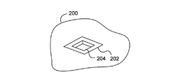
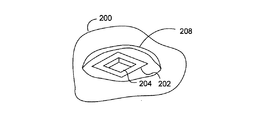
202 より大きな領域
204 より小さな領域
208 電解液
210 電極
212 第2の電極
220 付着構造
502 プローブ
504 選択エッチング剤
510 別の基板
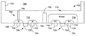
700 薄化された基板
702 CMOSトランジスタ
704 PチャネルMOSFET
706 N領域
712 P型基板領域
714 NチャネルMOSFET
716 P+領域
718 Nウェル領域
732 導電コンタクト
740 トレンチ
742 穴
750 電解液
752 電極
756 金属材料
760 キャップ
762 プローブ
Claims (9)
- 微小導電構造を製造する方法であって、
付着前駆体ガスが存在しない状況で基板表面に向かって集束ビームを誘導して、パターンの導電性を高めるために基板にイオンを注入することによって、導電シード・パターンを生成するステップと、
前記導電シード・パターンの少なくとも一部分を電解液で覆うステップと、
前記電解液を通して前記導電シード・パターンに電流を流して、前記導電シード・パターン上に導電材料を付着させるステップと
を含み、
前記基板表面に向かって集束ビームを誘導することが、半導体基板内へドーパント・イオンの集束ビームを誘導して、前記基板表面内にドーパント原子粒子を注入することを含み、
前記基板表面に向かって集束ビームを誘導することが、周期表の第13または第15族からなるグループからのイオンのビームを誘導することを含み、
前記基板が、周期表の第14族からなるグループからの材料からなる、方法。 - 基板表面に向かって集束ビームを誘導するステップが、荷電粒子ビームをある2次元パターンに誘導するステップを含む、請求項1に記載の方法。
- 前記基板をエッチングして、前記導電材料を取り出すステップをさらに含む、請求項1に記載の方法。
- 前記電流を監視して、前記導電シード・パターン上の導電材料の付着速度または付着量を決定するステップをさらに含む、請求項1または3に記載の方法。
- 微小導電構造を製造する方法であって、
前駆体ガスが存在しない状況で基板に向かってイオンまたは原子を誘導して、導電率が高められたパターン形成された領域を生成するステップと、
前記導電率が高められたパターン形成された領域の上に金属材料を電気化学付着させるステップと
前記基板に向かってイオンまたは原子を誘導することが、半導体基板内へドーパント・イオンの集束ビームを誘導して、前記基板内にドーパント原子粒子を注入することを含み、
前記基板に向かってイオンまたは原子を誘導することが、周期表の第13または第15族からなるグループからのイオンのビームを誘導することを含み、
前記基板が、周期表の第14族からなるグループからの材料からなる、方法。 - 前駆体ガスが存在しない状況で基板に向かってイオンまたは原子を誘導するステップが、前記基板に向かって集束イオン・ビームをあるパターンで走査するステップを含む、請求項5に記載の方法。
- 電着中に電流または電圧を監視して、電着の付着速度または付着量を決定するステップをさらに含む、請求項5または6に記載の方法。
- 前駆体ガスが存在しない状況で基板に向かってイオンまたは原子を誘導するステップが、
基板の上にフォトレジスト層を塗布するステップと、
前記フォトレジストを露光するステップと、
前記フォトレジストを現像して、露出した基板表面のパターンを残すステップと、
前記基板の露出した領域を、イオン・フラックスまたは原子フラックスに露出するステップと、
残ったフォトレジストを除去するステップと
を含む、請求項5〜7のいずれか一項に記載の方法。 - 前記基板の露出した領域を、イオン・フラックスまたは原子フラックスに露出するステップが、ドーパント・イオンまたはドーパント原子を注入することによって、前記露出した基板表面の導電率を増大させるステップを含む、請求項8に記載の方法。
Applications Claiming Priority (4)
| Application Number | Priority Date | Filing Date | Title |
|---|---|---|---|
| US8760508P | 2008-08-08 | 2008-08-08 | |
| US61/087,605 | 2008-08-08 | ||
| US12/210,781 US8278220B2 (en) | 2008-08-08 | 2008-09-15 | Method to direct pattern metals on a substrate |
| US12/210,781 | 2008-09-15 |
Related Child Applications (2)
| Application Number | Title | Priority Date | Filing Date |
|---|---|---|---|
| JP2014094903A Division JP2014187371A (ja) | 2008-08-08 | 2014-05-01 | 半導体試験方法 |
| JP2014094902A Division JP2014187370A (ja) | 2008-08-08 | 2014-05-01 | 微小金属構造の製造方法 |
Publications (3)
| Publication Number | Publication Date |
|---|---|
| JP2010045353A JP2010045353A (ja) | 2010-02-25 |
| JP2010045353A5 JP2010045353A5 (ja) | 2012-08-30 |
| JP5656311B2 true JP5656311B2 (ja) | 2015-01-21 |
Family
ID=41228378
Family Applications (3)
| Application Number | Title | Priority Date | Filing Date |
|---|---|---|---|
| JP2009182935A Expired - Fee Related JP5656311B2 (ja) | 2008-08-08 | 2009-08-06 | 基板上にパターン金属を誘導する方法 |
| JP2014094903A Withdrawn JP2014187371A (ja) | 2008-08-08 | 2014-05-01 | 半導体試験方法 |
| JP2014094902A Withdrawn JP2014187370A (ja) | 2008-08-08 | 2014-05-01 | 微小金属構造の製造方法 |
Family Applications After (2)
| Application Number | Title | Priority Date | Filing Date |
|---|---|---|---|
| JP2014094903A Withdrawn JP2014187371A (ja) | 2008-08-08 | 2014-05-01 | 半導体試験方法 |
| JP2014094902A Withdrawn JP2014187370A (ja) | 2008-08-08 | 2014-05-01 | 微小金属構造の製造方法 |
Country Status (3)
| Country | Link |
|---|---|
| US (1) | US8278220B2 (ja) |
| EP (2) | EP2151854A3 (ja) |
| JP (3) | JP5656311B2 (ja) |
Families Citing this family (22)
| Publication number | Priority date | Publication date | Assignee | Title |
|---|---|---|---|---|
| EP2199434A1 (en) * | 2008-12-19 | 2010-06-23 | FEI Company | Method for forming microscopic structures on a substrate |
| EP2226830B1 (en) | 2009-03-06 | 2014-01-08 | FEI Company | Charged particle beam processing |
| EP2261395A1 (en) * | 2009-06-12 | 2010-12-15 | Fei Company | Au-containing layer obtainable by charged particle beam processing |
| US8859998B2 (en) | 2011-01-28 | 2014-10-14 | Fei Company | TEM sample preparation |
| US8986524B2 (en) | 2011-01-28 | 2015-03-24 | International Business Machines Corporation | DNA sequence using multiple metal layer structure with different organic coatings forming different transient bondings to DNA |
| US8859963B2 (en) * | 2011-06-03 | 2014-10-14 | Fei Company | Methods for preparing thin samples for TEM imaging |
| JP2013101929A (ja) | 2011-11-07 | 2013-05-23 | Fei Co | 荷電粒子ビーム・システムの絞り |
| US9733164B2 (en) | 2012-06-11 | 2017-08-15 | Fei Company | Lamella creation method and device using fixed-angle beam and rotating sample stage |
| US8759764B2 (en) | 2012-06-29 | 2014-06-24 | Fei Company | On-axis detector for charged particle beam system |
| US9046511B2 (en) | 2013-04-18 | 2015-06-02 | International Business Machines Corporation | Fabrication of tunneling junction for nanopore DNA sequencing |
| US9182369B2 (en) | 2013-06-19 | 2015-11-10 | Globalfoundries Inc. | Manufacturable sub-3 nanometer palladium gap devices for fixed electrode tunneling recognition |
| US9188578B2 (en) | 2013-06-19 | 2015-11-17 | Globalfoundries Inc. | Nanogap device with capped nanowire structures |
| JP6290559B2 (ja) * | 2013-09-03 | 2018-03-07 | 株式会社日立ハイテクサイエンス | 断面加工観察方法、断面加工観察装置 |
| KR101565673B1 (ko) * | 2014-01-02 | 2015-11-03 | 삼성전기주식회사 | 칩 전자부품의 제조방법 |
| CA2948148C (en) * | 2014-05-09 | 2022-12-06 | AuroMedics Pharma LLC | Formulations of cyclophosphamide liquid concentrate |
| EP3043372B1 (en) | 2015-01-12 | 2017-01-04 | Fei Company | Method of modifying a sample surface layer from a microscopic sample |
| US10103008B2 (en) | 2016-01-12 | 2018-10-16 | Fei Company | Charged particle beam-induced etching |
| EP3249676B1 (en) | 2016-05-27 | 2018-10-03 | FEI Company | Dual-beam charged-particle microscope with in situ deposition functionality |
| ES2738911A1 (es) * | 2018-07-25 | 2020-01-27 | Consejo Superior Investigacion | Procedimiento para depositar elementos sobre un sustrato de interes y dispositivo |
| US11298547B2 (en) | 2018-07-27 | 2022-04-12 | Medtronic, Inc. | Fluid status detection from a cardiac electrical signal and impedance signal |
| CN111413727B (zh) * | 2020-04-15 | 2021-12-28 | 中国科学院电工研究所 | 一种电子束发散角测量装置及其制备方法和测量方法 |
| US20230369211A1 (en) * | 2022-05-13 | 2023-11-16 | Intel Corporation | Designs to enable inline circuit edit |
Family Cites Families (23)
| Publication number | Priority date | Publication date | Assignee | Title |
|---|---|---|---|---|
| US3013955A (en) | 1959-04-29 | 1961-12-19 | Fairchild Camera Instr Co | Method of transistor manufacture |
| US3043955A (en) | 1960-01-25 | 1962-07-10 | Hughes Aircraft Co | Discriminating radiation detector |
| GB1062365A (en) | 1965-03-01 | 1967-03-22 | Hughes Aircraft Co | A method of electroplating an ohmic contact bump upon a semiconductor body |
| US3506545A (en) * | 1967-02-14 | 1970-04-14 | Ibm | Method for plating conductive patterns with high resolution |
| JPS60143630A (ja) * | 1983-12-29 | 1985-07-29 | Fujitsu Ltd | イオン注入方法 |
| JPS60145612A (ja) * | 1984-01-09 | 1985-08-01 | Mitsubishi Electric Corp | 半導体装置の製造方法 |
| JPS63210845A (ja) * | 1987-02-27 | 1988-09-01 | Hitachi Ltd | 欠陥修正方法 |
| US4874460A (en) | 1987-11-16 | 1989-10-17 | Seiko Instruments Inc. | Method and apparatus for modifying patterned film |
| JP2553926B2 (ja) * | 1989-01-25 | 1996-11-13 | 理化学研究所 | 選択的金属薄膜の形成方法 |
| US6153891A (en) | 1994-11-23 | 2000-11-28 | Intel Corporation | Method and apparatus providing a circuit edit structure through the back side of an integrated circuit die |
| US5976980A (en) | 1994-11-23 | 1999-11-02 | Intel Corporation | Method and apparatus providing a mechanical probe structure in an integrated circuit die |
| JP2000232078A (ja) | 1999-02-10 | 2000-08-22 | Toshiba Corp | メッキ方法及びメッキ装置 |
| US6319831B1 (en) | 1999-03-18 | 2001-11-20 | Taiwan Semiconductor Manufacturing Company | Gap filling by two-step plating |
| JP3541931B2 (ja) | 1999-05-17 | 2004-07-14 | 富士ゼロックス株式会社 | 電着膜形成方法、電極形成方法および電着膜形成装置 |
| US6372529B1 (en) | 1999-09-30 | 2002-04-16 | Advanced Micro Devices, Inc. | Forming elongated probe points useful in testing semiconductor devices |
| US6838380B2 (en) | 2001-01-26 | 2005-01-04 | Fei Company | Fabrication of high resistivity structures using focused ion beams |
| US6815358B2 (en) * | 2001-09-06 | 2004-11-09 | Seagate Technology Llc | Electron beam lithography method for plating sub-100 nm trenches |
| KR100465063B1 (ko) | 2002-04-01 | 2005-01-06 | 주식회사 하이닉스반도체 | 반도체 소자의 금속배선 형성방법 |
| US6974768B1 (en) | 2003-01-15 | 2005-12-13 | Novellus Systems, Inc. | Methods of providing an adhesion layer for adhesion of barrier and/or seed layers to dielectric films |
| US6958248B1 (en) * | 2003-02-28 | 2005-10-25 | Credence Systems Corporation | Method and apparatus for the improvement of material/voltage contrast |
| US7674706B2 (en) * | 2004-04-13 | 2010-03-09 | Fei Company | System for modifying small structures using localized charge transfer mechanism to remove or deposit material |
| US20060251801A1 (en) | 2005-03-18 | 2006-11-09 | Weidman Timothy W | In-situ silicidation metallization process |
| EP1890136A1 (en) | 2006-08-16 | 2008-02-20 | FEI Company | Method for obtaining images from slices of a specimen |
-
2008
- 2008-09-15 US US12/210,781 patent/US8278220B2/en not_active Expired - Fee Related
-
2009
- 2009-08-06 EP EP09167311A patent/EP2151854A3/en not_active Ceased
- 2009-08-06 EP EP09167312A patent/EP2151859A3/en not_active Withdrawn
- 2009-08-06 JP JP2009182935A patent/JP5656311B2/ja not_active Expired - Fee Related
-
2014
- 2014-05-01 JP JP2014094903A patent/JP2014187371A/ja not_active Withdrawn
- 2014-05-01 JP JP2014094902A patent/JP2014187370A/ja not_active Withdrawn
Also Published As
| Publication number | Publication date |
|---|---|
| EP2151854A3 (en) | 2011-11-16 |
| JP2014187370A (ja) | 2014-10-02 |
| US8278220B2 (en) | 2012-10-02 |
| JP2010045353A (ja) | 2010-02-25 |
| EP2151854A2 (en) | 2010-02-10 |
| EP2151859A3 (en) | 2011-08-17 |
| US20100032302A1 (en) | 2010-02-11 |
| JP2014187371A (ja) | 2014-10-02 |
| EP2151859A2 (en) | 2010-02-10 |
Similar Documents
| Publication | Publication Date | Title |
|---|---|---|
| JP5656311B2 (ja) | 基板上にパターン金属を誘導する方法 | |
| KR101290681B1 (ko) | 소구조물 변경 시스템 | |
| US9812286B2 (en) | Localized, in-vacuum modification of small structures | |
| US11999016B2 (en) | Methods of forming parts using laser machining | |
| US8557707B2 (en) | Focused ion beam deep nano-patterning apparatus and method | |
| US7902062B2 (en) | Electrodepositing a metal in integrated circuit applications | |
| KR20250105457A (ko) | 깊은 다중층 구조의 개선된 편집 | |
| CN100592466C (zh) | 用于修改小结构的系统 | |
| Park et al. | FIB overview | |
| TWI902278B (zh) | 離子束掃描半導體樣品之方法及檢查和修復系統 | |
| JP2002075849A (ja) | 電子ビーム露光装置、荷電粒子線を整形する部材及びその製造方法 | |
| JP2011179959A (ja) | 電気特性測定用試料の作製方法、測定方法及び試料加工測定装置 | |
| RU2762129C2 (ru) | Способ обработки несогласованностей в устройствах на основе солнечных элементов и устройства, полученные с его помощью | |
| JP2006507675A (ja) | 金属、特に銅を電着する方法、この方法の使用、および集積回路構造 | |
| HK40115207A (zh) | 利用导电材料沉积在半导体上以产生相变和欧姆接触所形成的半导体器件及其制造方法 | |
| JP2002222725A (ja) | 薄膜インダクタの製造方法 | |
| KR100238237B1 (ko) | 전자빔 셀 투영 리소그래피용 마스크 및 그 제조방법 | |
| Cheng | Metallic nanotransistors |
Legal Events
| Date | Code | Title | Description |
|---|---|---|---|
| A521 | Request for written amendment filed |
Free format text: JAPANESE INTERMEDIATE CODE: A523 Effective date: 20120714 |
|
| A621 | Written request for application examination |
Free format text: JAPANESE INTERMEDIATE CODE: A621 Effective date: 20120714 |
|
| A977 | Report on retrieval |
Free format text: JAPANESE INTERMEDIATE CODE: A971007 Effective date: 20130930 |
|
| A131 | Notification of reasons for refusal |
Free format text: JAPANESE INTERMEDIATE CODE: A131 Effective date: 20131101 |
|
| A601 | Written request for extension of time |
Free format text: JAPANESE INTERMEDIATE CODE: A601 Effective date: 20140131 |
|
| A602 | Written permission of extension of time |
Free format text: JAPANESE INTERMEDIATE CODE: A602 Effective date: 20140205 |
|
| A601 | Written request for extension of time |
Free format text: JAPANESE INTERMEDIATE CODE: A601 Effective date: 20140226 |
|
| A602 | Written permission of extension of time |
Free format text: JAPANESE INTERMEDIATE CODE: A602 Effective date: 20140303 |
|
| A601 | Written request for extension of time |
Free format text: JAPANESE INTERMEDIATE CODE: A601 Effective date: 20140331 |
|
| A602 | Written permission of extension of time |
Free format text: JAPANESE INTERMEDIATE CODE: A602 Effective date: 20140403 |
|
| A521 | Request for written amendment filed |
Free format text: JAPANESE INTERMEDIATE CODE: A523 Effective date: 20140430 |
|
| A131 | Notification of reasons for refusal |
Free format text: JAPANESE INTERMEDIATE CODE: A131 Effective date: 20140527 |
|
| A601 | Written request for extension of time |
Free format text: JAPANESE INTERMEDIATE CODE: A601 Effective date: 20140826 |
|
| A602 | Written permission of extension of time |
Free format text: JAPANESE INTERMEDIATE CODE: A602 Effective date: 20140829 |
|
| A521 | Request for written amendment filed |
Free format text: JAPANESE INTERMEDIATE CODE: A523 Effective date: 20140925 |
|
| TRDD | Decision of grant or rejection written | ||
| A01 | Written decision to grant a patent or to grant a registration (utility model) |
Free format text: JAPANESE INTERMEDIATE CODE: A01 Effective date: 20141024 |
|
| A61 | First payment of annual fees (during grant procedure) |
Free format text: JAPANESE INTERMEDIATE CODE: A61 Effective date: 20141122 |
|
| R150 | Certificate of patent or registration of utility model |
Ref document number: 5656311 Country of ref document: JP Free format text: JAPANESE INTERMEDIATE CODE: R150 |
|
| R250 | Receipt of annual fees |
Free format text: JAPANESE INTERMEDIATE CODE: R250 |
|
| R250 | Receipt of annual fees |
Free format text: JAPANESE INTERMEDIATE CODE: R250 |
|
| LAPS | Cancellation because of no payment of annual fees |