JP5630552B2 - Silicon carbide semiconductor device and manufacturing method thereof - Google Patents
Silicon carbide semiconductor device and manufacturing method thereof Download PDFInfo
- Publication number
- JP5630552B2 JP5630552B2 JP2013215126A JP2013215126A JP5630552B2 JP 5630552 B2 JP5630552 B2 JP 5630552B2 JP 2013215126 A JP2013215126 A JP 2013215126A JP 2013215126 A JP2013215126 A JP 2013215126A JP 5630552 B2 JP5630552 B2 JP 5630552B2
- Authority
- JP
- Japan
- Prior art keywords
- conductivity type
- base layer
- region
- layer
- type base
- Prior art date
- Legal status (The legal status is an assumption and is not a legal conclusion. Google has not performed a legal analysis and makes no representation as to the accuracy of the status listed.)
- Expired - Fee Related
Links
Images


Landscapes
- Electrodes Of Semiconductors (AREA)
Description
この発明は、半導体材料として炭化珪素(SiC)を用いた炭化珪素半導体装置およびその製造方法に関する。 The present invention relates to a silicon carbide semiconductor device using silicon carbide (SiC) as a semiconductor material and a method for manufacturing the same.
従来、炭化珪素半導体材料は、シリコン半導体材料よりも大きなバンドギャップを有しているため、シリコン半導体材料よりも絶縁破壊電界強度が高いことが知られている。ここで、オン抵抗は、導通状態における抵抗であり、絶縁破壊電界強度の3乗に反比例する。このため、例えば広く用いられている4H型と呼ばれる炭化珪素半導体においては、オン抵抗をシリコン半導体の100分の1に抑制することができる。また、炭化珪素半導体は、熱伝導度が大きいため、放熱が容易である。これらの理由から、炭化珪素半導体を用いて作製される次世代の低損失な電力用半導体装置が期待されている。 Conventionally, a silicon carbide semiconductor material has a larger band gap than a silicon semiconductor material, so that it is known that a breakdown electric field strength is higher than that of a silicon semiconductor material. Here, the on-resistance is a resistance in a conductive state and is inversely proportional to the cube of the dielectric breakdown electric field strength. For this reason, for example, in a widely used silicon carbide semiconductor called 4H type, the on-resistance can be suppressed to 1/100 of that of a silicon semiconductor. Moreover, since a silicon carbide semiconductor has a large thermal conductivity, heat dissipation is easy. For these reasons, a next-generation low-loss power semiconductor device manufactured using a silicon carbide semiconductor is expected.
近年、炭化珪素半導体材料を用いた炭化珪素ウエハ(半導体基板)の品質向上や大口径化の進展にともなって、シリコン半導体材料を用いたシリコン半導体装置の特性を大きく上回る金属酸化物半導体電界効果型トランジスタ(MOSFET)、バイポーラトランジスタ、接合型電界効果型トランジスタ(JFET)などの開発が盛んである。特にMOSFETは、電圧駆動型素子であるため、ゲート駆動回路を低コストに抑えることができる。また、MOSFETは、電子あるいは正孔のみの多数キャリア素子であって導通時の素子内にキャリアの蓄積がないため、ターンオフ時にそれらのキャリアを素子外に掃き出す時間を必要としない。したがって、例えば電子および正孔の両方が伝導に寄与するバイポーラ型素子と比較して高速スイッチングが可能となる。 In recent years, as the quality of silicon carbide wafers (semiconductor substrates) using silicon carbide semiconductor materials improves and the diameter increases, the metal oxide semiconductor field effect type greatly exceeds the characteristics of silicon semiconductor devices using silicon semiconductor materials. The development of transistors (MOSFETs), bipolar transistors, junction field effect transistors (JFETs), and the like is active. In particular, since the MOSFET is a voltage-driven element, the gate driving circuit can be suppressed at a low cost. Further, since the MOSFET is a majority carrier element having only electrons or holes and does not accumulate carriers in the conductive element, it does not require time for sweeping out the carriers out of the element at the time of turn-off. Therefore, for example, high-speed switching is possible as compared with a bipolar element in which both electrons and holes contribute to conduction.
なお、本明細書において、nまたはpを冠した半導体は、それぞれ電子、正孔が多数キャリアであることを意味する。また、n+やn-などのように、nやpに付す「+」または「-」は、それぞれそれらが付されていない半導体の不純物濃度よりも比較的高濃度または比較的低濃度であることを表す。 Note that in this specification, a semiconductor having n or p means that electrons and holes are majority carriers, respectively. Further, “ + ” or “ − ” attached to n or p, such as n + or n −, is relatively higher or lower than the impurity concentration of the semiconductor to which they are not attached. Represents that.
図6は、従来の一般的な縦型MOSFET(DIMOSFET)の断面構造について示す断面図である。図6に示すように、DIMOSFETは、n+型ドレイン層21の上に、n-型ドリフト層22が設けられており、n-型ドリフト層22の表面層に、選択的にp型ベース層23が設けられている。すなわち、おもて面側の表面付近において、n-型ドリフト層22がp型ベース層23に挟まれた構造となっている。そして、p型ベース層23の表面層に、n-型ドリフト層22と離れてn+型ソース領域24が設けられている。また、p型ベース層23のn-型ドリフト層22とn+型ソース領域24に挟まれた領域と、n-型ドリフト層22との上に、ゲート酸化膜26を介してゲート電極27が設けられている。さらに、おもて面側にソース/ベース電極28が設けられ、裏面側にドレイン電極29が設けられている。
FIG. 6 is a cross-sectional view showing a cross-sectional structure of a conventional general vertical MOSFET (DIMOSFET). As shown in FIG. 6, in the DIMOSFET, an n −
図6に示すDIMOSFETにおいては、n-型ドリフト層22においてゲート酸化膜26との界面近傍を電子が移動するときに蓄積層抵抗が生じる。また、n-型ドリフト層22内のゲート酸化膜26との界面近傍から裏面側のドレインに向かって電流が流れるときに、n-型ドリフト層22がp型ベース層23に挟まれているために、JFET抵抗が発生しやすい。
In the DIMOSFET shown in FIG. 6, accumulation layer resistance is generated when electrons move in the vicinity of the interface with the
上述した蓄積層抵抗やJFET抵抗を生じさせないために、トレンチゲート構造を有するMOSFET(UMOSFET)が提案されている。図7は、従来の一般的なUMOSFETの断面構造を示す断面図である。UMOSFETは、主面に対して側壁が垂直なトレンチゲートを有するMOSFETである。図7においては、UMOSFETの1セルピッチの断面構造を示している。 In order to prevent the above-described accumulation layer resistance and JFET resistance from occurring, a MOSFET (UMOSFET) having a trench gate structure has been proposed. FIG. 7 is a sectional view showing a sectional structure of a conventional general UMOSFET. The UMOSFET is a MOSFET having a trench gate whose side wall is perpendicular to the main surface. FIG. 7 shows a cross-sectional structure of one cell pitch of UMOSFET.
図7に示すように、UMOSFETを作製する際には、n+型ドレイン層31となる比較的低い抵抗率のn+型炭化珪素基板の上に、比較的高い抵抗率のn-型ドリフト層32と、p型ベース層33とを、この順にエピタキシャルSiC成長により形成する。そして、p型ベース層33の表面からイオン注入を行うことでn+型ソース領域34を形成する。このような炭化珪素ウェハに、n-型ドリフト層32に達するようなゲートトレンチ35を形成し、ゲートトレンチ35内部に、ゲート酸化膜36を介してゲート電極37を形成する。さらに、炭化珪素ウェハ30のおもて面側にソース/ベース電極38を形成し、裏面側にドレイン電極39を形成することで、UMOSFETが完成する。
As shown in FIG. 7, when manufacturing a UMOSFET, an n − type drift layer having a relatively high resistivity is formed on an n + type silicon carbide substrate having a relatively low resistivity to be an n +
図7に示すUMOSFETにおいては、オフ状態時に、ソース/ベース電極38をアース電位にしておき、ゲート電極37に十分に大きな負バイアスを印加することで、電流が流れなくなる。その理由は、p型ベース層33のn+型ソース領域34とn-型ドリフト層32に挟まれた領域と、ゲート酸化膜36との界面近傍において、正孔が誘起された蓄積状態となり、伝導キャリアである電子の経路が遮断されるためである。また、ドレイン電極39に正の高電圧を印加するとp型ベース層33とn-型ドリフト層32間の接合が逆バイアス状態になるので、空乏層がp型ベース層33内とn-型ドリフト層32内に広がり、電流を低く抑えたまま高電圧が維持される。
In the UMOSFET shown in FIG. 7, when the source /
また、オン状態時に、ゲート電極37に十分に大きな正バイアスを印加することで、p型ベース層33のn+型ソース領域34とn-型ドリフト層32に挟まれた領域と、ゲート酸化膜36との界面近傍において、電子が誘起された反転状態となる。そして、ソース/ベース電極38、n+型ソース領域34、p型ベース層33のゲート酸化膜36に接する反転層(不図示)、n-型ドリフト層32、n+型ドレイン層31、ドレイン電極39の順にキャリアが流れる。
Further, when a sufficiently large positive bias is applied to the gate electrode 37 in the on state, the region sandwiched between the n +
このように、図6に示すDIMOSFETではセルピッチを小さくしていくと、所定のセルピッチ距離からJFET抵抗が現れて、オン抵抗が増加するのに対し、図7に示すUMOSFETではセルピッチを小さくすればするほどオン抵抗が単調に減少する。特に、約3kV以下の耐圧を持つMOSFETにおいては、MOSチャネル抵抗が無視できないために微細化によるセルピッチの縮小が必須であり、この場合UMOSFETの方が適している。 As described above, when the cell pitch is reduced in the DIMOSFET shown in FIG. 6, the JFET resistance appears from a predetermined cell pitch distance and the on-resistance increases, whereas in the UMOSFET shown in FIG. 7, the cell pitch is reduced. The on-resistance decreases monotonously. In particular, in a MOSFET having a withstand voltage of about 3 kV or less, since the MOS channel resistance cannot be ignored, the cell pitch must be reduced by miniaturization, and in this case, the UMOSFET is more suitable.
しかしながら、UMOSFETにおいては、ゲートトレンチ35底部においてゲート酸化膜36(SiO2膜)に印加される電界強度が非常に大きくなる。その理由は、炭化珪素の比誘電率(4H−SiCの場合、例えば9.7)と、SiO2の比誘電率(例えば3.8)とが異なるためである。また、図示は省略したが、ゲートトレンチ35の角部の酸化膜に印加される電界強度は、電界集中のためにさらに大きくなる。 However, in the UMOSFET, the electric field strength applied to the gate oxide film 36 (SiO 2 film) at the bottom of the gate trench 35 becomes very large. The reason is that the relative dielectric constant of silicon carbide (for example, 9.7 in the case of 4H—SiC) and the relative dielectric constant of SiO 2 (for example, 3.8) are different. Although not shown, the electric field strength applied to the oxide film at the corner of the gate trench 35 is further increased due to electric field concentration.
そして、p型ベース層33とn-型ドリフト層32との間のpn接合部における電界強度のピークが炭化珪素の絶縁破壊電界強度(例えば、約2MV/cm)に達する前に、ゲートトレンチ35底部のゲート酸化膜36が酸化膜の絶縁破壊電界強度(例えば、約10MV/cm)に先に達してしまい、理論耐圧よりも低い電圧で絶縁破壊を起こしてしまうという問題がある。
Then, before the peak of the electric field strength at the pn junction between the p-
このため、p型ベース層33のゲートトレンチ35同士の間の領域が、ゲートトレンチ35近傍よりも深く設けられたUMOSFETが提案されている(例えば、下記特許文献1参照。)。このUMOSFETでは、電界強度のピークがゲート酸化膜36から離れた位置になるので、ゲートトレンチ35の角部に電界集中するのを防ぐことができる。
For this reason, a UMOSFET in which a region between the gate trenches 35 of the p-
ここで、UMOSFETにおいては、電位を保つためにp型ベース層33が外部端子とオーミック接触をする必要がある。さらに、オーミック接触における接触抵抗はできるだけ小さいことが望ましい。その理由は、接触抵抗が大きいと素子のRC回路の時定数が増加し、スイッチング損失となるからである。そのためには、比較的高いドーズ量のAl(アルミニウム)イオンを注入する必要がある。
Here, in the UMOSFET, the p-
しかしながら、上述した技術のように、高いドーズ量でAlイオンを注入すると、リーク電流が増加し、絶縁耐圧が低下するという問題がある。特に、基板表面をSi面またはC面とし、p型ベース層におけるボディコンタクト領域にらせん転位が含まれていると、高い確率でリーク電流が増加する。p型ベース層をエピタキシャル成長により形成する場合、p型ベース層の厚さを大きくすればリーク電流を減少させることはできるが、チャネル長が増加するため、チャネル抵抗が増加するという問題がある。 However, when Al ions are implanted with a high dose as in the technique described above, there is a problem that the leakage current increases and the withstand voltage decreases. In particular, when the substrate surface is a Si plane or C plane and the screw contact is included in the body contact region in the p-type base layer, the leakage current increases with a high probability. When the p-type base layer is formed by epitaxial growth, the leakage current can be reduced if the thickness of the p-type base layer is increased, but there is a problem that the channel resistance increases because the channel length increases.
この発明は、上述した従来技術による問題点を解消するため、リーク電流を抑え、かつチャネル抵抗を低減することができる炭化珪素半導体装置およびその製造方法を提供することを目的とする。 An object of the present invention is to provide a silicon carbide semiconductor device capable of suppressing leakage current and reducing channel resistance, and a method for manufacturing the same, in order to solve the above-described problems caused by the prior art.
上述した課題を解決し、目的を達成するため、この発明にかかる炭化珪素半導体装置は、第1導電型炭化珪素半導体基板のおもて面側の全面に設けられた第1導電型ドリフト層と、前記第1導電型ドリフト層の全面に設けられた第2導電型ベース層と、前記第2導電型ベース層の表面層に選択的に設けられた第2導電型不純物領域と、前記第2導電型ベース層の表面層に、前記第2導電型不純物領域と離れて設けられたトレンチと、前記トレンチの内部に、ゲート酸化膜を介して埋め込まれたゲート電極と、前記第2導電型ベース層の表面層に、前記トレンチと接し、前記第2導電型不純物領域と離れて設けられた第1導電型ソース領域と、前記ゲート電極を覆うように設けられた絶縁膜と、前記第2導電型不純物領域および前記第1導電型ソース領域に接するように設けられたソース電極と、前記第1導電型炭化珪素半導体基板の裏面側に設けられたドレイン電極と、を備え、前記第2導電型ベース層の、前記第2導電型不純物領域と前記第1導電型ドリフト層とに挟まれた部分の厚さは、前記第2導電型ベース層の、前記第2導電型不純物領域と前記第1導電型ドリフト層とに挟まれた部分以外の領域の厚さよりも厚く、前記第2導電型ベース層の、前記第2導電型不純物領域と前記第1導電型ドリフト層とに挟まれた部分は、前記第2導電型ベース層の、前記第2導電型不純物領域と前記第1導電型ドリフト層とに挟まれた部分以外の領域よりも前記ソース電極側に突出していることを特徴とする。 In order to solve the above-described problems and achieve the object, a silicon carbide semiconductor device according to the present invention includes a first conductivity type drift layer provided on the entire front surface side of a first conductivity type silicon carbide semiconductor substrate, and A second conductivity type base layer provided on the entire surface of the first conductivity type drift layer; a second conductivity type impurity region selectively provided on a surface layer of the second conductivity type base layer; A trench provided in a surface layer of the conductivity type base layer apart from the second conductivity type impurity region; a gate electrode embedded in the trench through a gate oxide film; and the second conductivity type base. A first conductivity type source region provided in contact with the trench and spaced apart from the second conductivity type impurity region, an insulating film provided to cover the gate electrode, and the second conductivity Type impurity region and the first conductivity type A source electrode provided in contact with the source region, and a drain electrode provided on the back surface side of the first conductivity type silicon carbide semiconductor substrate, wherein the second conductivity type base layer includes the second conductivity type. The thickness of the portion sandwiched between the type impurity region and the first conductivity type drift layer is set between the second conductivity type impurity region and the first conductivity type drift layer of the second conductivity type base layer. The portion of the second conductivity type base layer sandwiched between the second conductivity type impurity region and the first conductivity type drift layer is thicker than the thickness of the region other than the region where the second conductivity type base layer is formed. In this case, the region protrudes more toward the source electrode than the region other than the portion sandwiched between the second conductivity type impurity region and the first conductivity type drift layer.
また、この発明にかかる炭化珪素半導体装置は、上述した発明において、前記第2導電型不純物領域の底部から前記第2導電型ベース層と前記第1導電型ドリフト層との界面までの距離は、4μm以上であることを特徴とする。 In the silicon carbide semiconductor device according to the present invention, in the above-described invention, the distance from the bottom of the second conductivity type impurity region to the interface between the second conductivity type base layer and the first conductivity type drift layer is: It is characterized by being 4 μm or more.
また、この発明にかかる炭化珪素半導体装置の製造方法は、第1導電型炭化珪素半導体基板のおもて面側の全面に第1導電型ドリフト層を積層する工程と、前記第1導電型ドリフト層の全面に第2導電型ベース層を積層する工程と、前記第2導電型ベース層を所定深さでかつ選択的にエッチングし、前記第2導電型ベース層の一部を突出領域として残す工程と、前記突出領域の表面層に第2導電型不純物領域を形成する工程と、前記第2導電型ベース層の表面層の、前記突出領域以外の領域に第1導電型ソース領域を形成する工程と、前記第1導電型ソース領域および前記第2導電型ベース層を貫通するように第2トレンチを形成する工程と、前記第2トレンチの内部に、ゲート酸化膜を介してゲート電極を形成する工程と、前記第1導電型ソース領域および前記第2導電型不純物領域に接するようにソース電極を形成する工程と、前記第1導電型炭化珪素半導体基板の裏面側にドレイン電極を形成する工程と、を含むことを特徴とする。 A method for manufacturing a silicon carbide semiconductor device according to the present invention includes a step of laminating a first conductivity type drift layer on the entire front surface side of a first conductivity type silicon carbide semiconductor substrate, and the first conductivity type drift. A step of laminating a second conductivity type base layer on the entire surface of the layer, and selectively etching the second conductivity type base layer at a predetermined depth, leaving a part of the second conductivity type base layer as a protruding region. Forming a second conductivity type impurity region in the surface layer of the protruding region; and forming a first conductivity type source region in a region other than the protruding region of the surface layer of the second conductivity type base layer. Forming a second trench so as to penetrate the first conductive type source region and the second conductive type base layer; and forming a gate electrode inside the second trench through a gate oxide film And the first conductivity type Forming a source electrode so as to be in contact with a source region and the second conductivity type impurity region, and forming a drain electrode on the back surface side of the first conductivity type silicon carbide semiconductor substrate, To do.
また、この発明にかかる炭化珪素半導体装置の製造方法は、上述した発明において、前記第2導電型ベース層を積層する工程においては、厚さが4μm以上となるように、前記第1導電型ドリフト層の全面に前記第2導電型ベース層を積層することを特徴とする。 In the method of manufacturing a silicon carbide semiconductor device according to the present invention, in the above-described invention, in the step of laminating the second conductivity type base layer, the first conductivity type drift is performed so that the thickness becomes 4 μm or more. The second conductivity type base layer is laminated on the entire surface of the layer.
上述した各請求項の発明によれば、第2導電型ベース層において、第2導電型ベース層よりも不純物濃度の高い第2導電型不純物領域が形成された領域は、第2導電型ベース層の表面から第2導電型ベース層と第1導電型ドリフト層との界面までの距離が比較的長い。具体的には、表面層に第2導電型不純物領域が形成された領域において、第2導電型ベース層の厚さが4μm以上である。したがって、リーク電流を減少することができる。また、第2導電型ベース層全体を厚くすると、チャネル抵抗が増加するという問題があるが、第2導電型ベース層において、表面層に第2導電型不純物領域が形成された領域以外は、第2導電型ベース層の表面から第2導電型ベース層と第1導電型ドリフト層との界面までの距離が比較的短いため、チャネル抵抗を低減することができる。 According to the invention of each claim described above, in the second conductivity type base layer, the region where the second conductivity type impurity region having an impurity concentration higher than that of the second conductivity type base layer is formed is the second conductivity type base layer. The distance from the surface of the substrate to the interface between the second conductivity type base layer and the first conductivity type drift layer is relatively long. Specifically, in the region where the second conductivity type impurity region is formed in the surface layer, the thickness of the second conductivity type base layer is 4 μm or more. Therefore, the leakage current can be reduced. Further, there is a problem that the channel resistance increases when the entire second conductivity type base layer is thickened. However, in the second conductivity type base layer, except for the region where the second conductivity type impurity region is formed in the surface layer, the second conductivity type base layer is increased. Since the distance from the surface of the two conductivity type base layer to the interface between the second conductivity type base layer and the first conductivity type drift layer is relatively short, the channel resistance can be reduced.
本発明にかかる炭化珪素半導体装置およびその製造方法によれば、リーク電流を抑え、かつチャネル抵抗を低減することができるという効果を奏する。 According to the silicon carbide semiconductor device and the manufacturing method thereof according to the present invention, it is possible to suppress the leak current and reduce the channel resistance.
以下に添付図面を参照して、この発明にかかる炭化珪素半導体装置およびその製造方法の好適な実施の形態を詳細に説明する。なお、各実施の形態の説明およびすべての添付図面において、同様の構成には同一の符号を付し、重複する説明を省略する。 Exemplary embodiments of a silicon carbide semiconductor device and a method for manufacturing the same according to the present invention will be described below in detail with reference to the accompanying drawings. Note that, in the description of each embodiment and all the attached drawings, the same reference numerals are given to the same components, and duplicate descriptions are omitted.
(実施の形態1)
まず、実施の形態1にかかる半導体装置について説明する。図1は、実施の形態1にかかる半導体装置の断面構造について示す断面図である。実施の形態1にかかる半導体装置は、エピタキシャルウエハーを用いて作製される。エピタキシャルウエハーは、n+型4
H−SiC基板1の上に、n型バッファー層2と、n-型ドリフト層3とが、この順に積
層されている。
(Embodiment 1)
First, the semiconductor device according to the first embodiment will be described. FIG. 1 is a cross-sectional view illustrating a cross-sectional structure of the semiconductor device according to the first embodiment. The semiconductor device according to the first embodiment is manufactured using an epitaxial wafer. The epitaxial wafer is n + type 4
On the H—
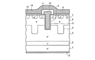
エピタキシャルウエハーには、第1主面から垂直に、第1トレンチ4が設けられている。そして、第1トレンチ4を有するエピタキシャルウエハーの全面にp型ベース層5が積層されている。したがって、第1トレンチ4には、p型ベース層5が埋め込まれている。
The epitaxial wafer is provided with a
p+型ボディコンタクト領域6は、第1トレンチ4が形成された領域の上の、p型ベース層5の表面層に設けられている。また、ゲートトレンチ(第2トレンチ)8は、第1トレンチ4が形成されていない領域に、p型ベース層5の表面層から設けられている。第2トレンチ8の内部には、ゲート酸化膜9を介してゲート電極10が埋め込まれている。また、n+型ソース領域7は、p型ベース層5の表面層に、第2トレンチ8と接し、p+型ボディコンタクト領域6と離れて設けられている。
The p + type
層間絶縁膜11は、ゲート電極10を覆うように設けられている。ソース電極12は、p+型ボディコンタクト領域6と、n+型ソース領域7とに接する。ドレイン電極13は、エピタキシャルウエハーの第2主面側に設けられている。ソース電極12および層間絶縁膜11の上にはメタル14が積層されている。
The
つぎに、実施の形態1にかかる半導体装置の製造方法について説明する。図2および図3は、実施の形態1にかかる半導体装置の製造方法を順に示す断面図である。まず、図2に示すように、厚さが例えば約400μmであり、不純物濃度が例えば1×1018cm-3であるn+型4H−SiC基板1を用意する。n+型4H−SiC基板1は、主面が例えば<11−20>方向に8度のオフ角を有する(0001)Si面または(000−1)C面である。
Next, a method for manufacturing the semiconductor device according to the first embodiment will be described. 2 and 3 are cross-sectional views sequentially showing the method for manufacturing the semiconductor device according to the first embodiment. First, as shown in FIG. 2, an n + -type 4H—
そして、n+型4H−SiC基板1に、膜厚が例えば1μmであり、不純物濃度が例えば1×1017cm-3であるn型バッファー層2と、不純物濃度が例えば9×1015cm-3であるn-型ドリフト層3をこの順にエピタキシャル成長により形成する。これにより、エピタキシャルウエハーが生成される。
Then, the n + -type 4H—
つぎに、例えばRIE(Reactive Ion Etching)によって、エピタキシャルウエハーの第1主面側から、第1主面と垂直に、幅が例えば1μmの第1トレンチ4を形成する。第1トレンチ4の深さは、例えば2.5μm以上であり、n型バッファー層2に達しない深さとする。
Next, the
ついで、図3に示すように、第1トレンチ4の形成されたエピタキシャルウエハーの第1主面側の全面に、不純物濃度が例えば2×1017cm-3であり、深さが例えば2μmであるp型ベース層5を堆積する。これによって、第1トレンチ4の内部にp型ベース層5が埋め込まれ、p型ベース層5の第1主面側が平坦となる。
Next, as shown in FIG. 3, the impurity concentration is 2 × 10 17 cm −3 and the depth is 2 μm, for example, on the entire surface of the first main surface of the epitaxial wafer in which the
そして、イオン注入によって、p型ベース層5の表面層の、第1トレンチ4の形成された上の領域に、比較的高濃度のAlイオンを注入する。そして、活性化アニール処理を行い、深さが例えば0.5μmであり、不純物濃度が2×1020cm-3である、p+型ボディコンタクト領域6を形成する。このとき、p+型ボディコンタクト領域6の底部から第1トレンチ4の底部のpn接合(p型ベース層5とn-型ドリフト層3との界面)までの距離を4μm以上とする。
Then, a relatively high concentration of Al ions is implanted into the surface layer of the p-
さらに、p型ベース層5の表面層に、p+型ボディコンタクト領域6と接しないように、n+型ソース領域7を形成し、p型ベース層5の表面層の、第1トレンチ4の形成されていない上の領域から、第2トレンチ(ゲートトレンチ)8を形成する。そして、通常のトレンチゲート型MOSFETを形成するように、ゲート酸化膜9、ゲート電極10、層間絶縁膜11、ソース電極12、ドレイン電極13およびメタル14を順次形成して、図1に示す半導体装置が完成する。
Further, an n +
ここで、例えば1.2kVクラスのMOSFETに実施の形態1の発明を適用した場合について検証を行った。実施の形態1の半導体装置では、リーク電流が10-8Aとなり、従来構造におけるリーク電流(10-4A)よりも低減した。また、実施の形態1の半導体装置では、チャネル抵抗が1mΩcm2となり、従来構造におけるチャネル抵抗(2mΩcm2)よりも低減した。 Here, for example, the case where the invention of the first embodiment is applied to a 1.2 kV class MOSFET was verified. In the semiconductor device of the first embodiment, the leakage current is 10 −8 A, which is lower than the leakage current (10 −4 A) in the conventional structure. In the semiconductor device of the first embodiment, the channel resistance is 1 mΩcm 2 , which is lower than the channel resistance ( 2 mΩcm 2 ) in the conventional structure.
実施の形態1によれば、p型ベース層5において、p型ベース層5よりも不純物濃度の高いp+型ボディコンタクト領域6が形成された領域は、p型ベース層5の表面からp型ベース層5とn-型ドリフト層3との界面までの距離が比較的長い。具体的には、表面層にp+型ボディコンタクト領域6が形成された領域において、p型ベース層5の厚さが4μm以上である。したがって、リーク電流を減少することができる。また、p型ベース層5全体を厚くすると、チャネル抵抗が増加するという問題があるが、p型ベース層5において、表面層にp+型ボディコンタクト領域6が形成された領域以外は、p型ベース層5の表面からp型ベース層5とn-型ドリフト層3との界面までの距離が比較的短いため、チャネル抵抗を低減することができる。
According to the first embodiment, in the p-
(実施の形態2)
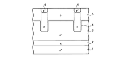
つぎに、実施の形態2にかかる半導体装置について説明する。図4は、実施の形態2にかかる半導体装置の断面構造について示す断面図である。図4に示すように、実施の形態2にかかる半導体装置は、第1トレンチが形成されず、p型ベース層5の一部が、第1主面から突き出た形状である。そして、p型ベース層5における突出領域15の表面層に、p+型ボディコンタクト領域6が設けられている。その他の構成は、実施の形態1と同様のため説明を省略する。
(Embodiment 2)
Next, a semiconductor device according to the second embodiment will be described. FIG. 4 is a cross-sectional view illustrating a cross-sectional structure of the semiconductor device according to the second embodiment. As shown in FIG. 4, in the semiconductor device according to the second embodiment, the first trench is not formed, and a part of the p-
つぎに、実施の形態2にかかる半導体装置の製造方法について説明する。図5は、実施の形態2にかかる半導体装置の製造方法を示す断面図である。図5に示すように、実施の形態2にかかる半導体装置は、まず、実施の形態1にかかる半導体装置と同様に、n+型4H−SiC基板1に、膜厚が例えば1μmであり、不純物濃度が例えば1×1017cm-3であるn型バッファー層2と、膜厚が例えば1μmであり、不純物濃度が例えば9×1015cm-3であるn-型ドリフト層3をこの順にエピタキシャル成長により形成する。これにより、エピタキシャルウエハーが生成される。
Next, a method for manufacturing the semiconductor device according to the second embodiment will be described. FIG. 5 is a cross-sectional view illustrating the method of manufacturing the semiconductor device according to the second embodiment. As shown in FIG. 5, in the semiconductor device according to the second embodiment, first, similarly to the semiconductor device according to the first embodiment, an n + -type 4H—
つぎに、エピタキシャルウエハーの全面に、深さが例えば4.5μm以上であり、不純物濃度が例えば2×1017cm-3である、p型ベース層5を積層する。そして、p型ベース層5の一部を残して、p型ベース層5の厚さが例えば2μmになるまで、ドライエッチングを行う。これによって、残されたp型ベース層5が突出領域15となる。
Next, the p-
つぎに、イオン注入によって、p型ベース層5の突出領域15の表面層に比較的高濃度のAlイオンを注入する。そして、活性化アニール処理を行うことで、深さが例えば0.5μmであり、不純物濃度が例えば2×1020cm-3である、p+型ボディコンタクト領域6を形成する。このとき、実施の形態1と同様に、p+型ボディコンタクト領域6の底部からpn接合(p型ベース層5とn-型ドリフト層3との界面)までの距離を4μm以上とする。以降の処理は、実施の形態1と同様のため説明を省略する。
Next, a relatively high concentration of Al ions is implanted into the surface layer of the protruding
実施の形態2によれば、実施の形態1と同様の効果を得ることができる。 According to the second embodiment, the same effect as in the first embodiment can be obtained.
なお、本実施の形態においては、第1導電型をn型とし、第2導電型をp型としたが、これに限るものではない。例えば、第2導電型をp型とし、第1導電型をn型としてもよい。 In the present embodiment, the first conductivity type is n-type and the second conductivity type is p-type. However, the present invention is not limited to this. For example, the second conductivity type may be p-type and the first conductivity type may be n-type.
以上のように、本発明にかかる炭化珪素半導体装置は、トレンチゲート構造を有するMOSFETやIGBTなどの炭化珪素半導体装置に有用であり、特に、MOS型電力用炭化珪素半導体装置に適している。 As described above, the silicon carbide semiconductor device according to the present invention is useful for silicon carbide semiconductor devices such as MOSFETs and IGBTs having a trench gate structure, and is particularly suitable for MOS power silicon carbide semiconductor devices.
1 n+型4H−SiC基板
2 n型バッファー層
3 n-型ドリフト層
4 第1トレンチ
5 p型ベース層
6 p+型ボディコンタクト領域
7 n+型ソース領域
8 第2トレンチ
9 ゲート酸化膜
10 ゲート電極
11 層間絶縁膜
12 ソース電極
13 ドレイン電極
14 メタル
1 n + type 4H-SiC substrate 2 n type buffer layer 3 n −
Claims (4)
前記第1導電型ドリフト層の全面に設けられた第2導電型ベース層と、
前記第2導電型ベース層の表面層に選択的に設けられた第2導電型不純物領域と、
前記第2導電型ベース層の表面層に、前記第2導電型不純物領域と離れて設けられたトレンチと、
前記トレンチの内部に、ゲート酸化膜を介して埋め込まれたゲート電極と、
前記第2導電型ベース層の表面層に、前記トレンチと接し、前記第2導電型不純物領域と離れて設けられた第1導電型ソース領域と、
前記ゲート電極を覆うように設けられた絶縁膜と、
前記第2導電型不純物領域および前記第1導電型ソース領域に接するように設けられたソース電極と、
前記第1導電型炭化珪素半導体基板の裏面側に設けられたドレイン電極と、
を備え、
前記第2導電型ベース層の、前記第2導電型不純物領域と前記第1導電型ドリフト層とに挟まれた部分の厚さは、前記第2導電型ベース層の、前記第2導電型不純物領域と前記第1導電型ドリフト層とに挟まれた部分以外の領域の厚さよりも厚く、
前記第2導電型ベース層の、前記第2導電型不純物領域と前記第1導電型ドリフト層とに挟まれた部分は、前記第2導電型ベース層の、前記第2導電型不純物領域と前記第1導電型ドリフト層とに挟まれた部分以外の領域よりも前記ソース電極側に突出していることを特徴とする炭化珪素半導体装置。 A first conductivity type drift layer provided on the entire front surface side of the first conductivity type silicon carbide semiconductor substrate;
A second conductivity type base layer provided on the entire surface of the first conductivity type drift layer;
A second conductivity type impurity region selectively provided in a surface layer of the second conductivity type base layer;
A trench provided in a surface layer of the second conductivity type base layer apart from the second conductivity type impurity region;
A gate electrode embedded in the trench via a gate oxide film;
A first conductivity type source region provided on a surface layer of the second conductivity type base layer in contact with the trench and spaced apart from the second conductivity type impurity region;
An insulating film provided to cover the gate electrode;
A source electrode provided in contact with the second conductivity type impurity region and the first conductivity type source region;
A drain electrode provided on the back side of the first conductivity type silicon carbide semiconductor substrate;
With
The thickness of the portion of the second conductivity type base layer sandwiched between the second conductivity type impurity region and the first conductivity type drift layer is equal to the thickness of the second conductivity type impurity of the second conductivity type base layer. Thicker than the thickness of the region other than the portion sandwiched between the region and the first conductivity type drift layer,
The portion of the second conductivity type base layer sandwiched between the second conductivity type impurity region and the first conductivity type drift layer is the same as the second conductivity type impurity region and the second conductivity type impurity region of the second conductivity type base layer. A silicon carbide semiconductor device, wherein the silicon carbide semiconductor device protrudes toward the source electrode from a region other than a portion sandwiched between the first conductivity type drift layers.
前記第1導電型ドリフト層の全面に第2導電型ベース層を積層する工程と、
前記第2導電型ベース層を所定深さでかつ選択的にエッチングし、前記第2導電型ベース層の一部を突出領域として残す工程と、
前記突出領域の表面層に第2導電型不純物領域を形成する工程と、
前記第2導電型ベース層の表面層の、前記突出領域以外の領域に第1導電型ソース領域を形成する工程と、
前記第1導電型ソース領域および前記第2導電型ベース層を貫通するように第2トレンチを形成する工程と、
前記第2トレンチの内部に、ゲート酸化膜を介してゲート電極を形成する工程と、
前記第1導電型ソース領域および前記第2導電型不純物領域に接するようにソース電極を形成する工程と、
前記第1導電型炭化珪素半導体基板の裏面側にドレイン電極を形成する工程と、
を含むことを特徴とする炭化珪素半導体装置の製造方法。 Laminating a first conductivity type drift layer over the entire front surface side of the first conductivity type silicon carbide semiconductor substrate;
Laminating a second conductivity type base layer over the entire surface of the first conductivity type drift layer;
Etching the second conductivity type base layer at a predetermined depth and selectively, leaving a part of the second conductivity type base layer as a protruding region;
Forming a second conductivity type impurity region in the surface layer of the protruding region;
Forming a first conductivity type source region in a region other than the protruding region of the surface layer of the second conductivity type base layer;
Forming a second trench so as to penetrate the first conductivity type source region and the second conductivity type base layer;
Forming a gate electrode inside the second trench through a gate oxide film;
Forming a source electrode so as to be in contact with the first conductivity type source region and the second conductivity type impurity region;
Forming a drain electrode on the back side of the first conductivity type silicon carbide semiconductor substrate;
The manufacturing method of the silicon carbide semiconductor device characterized by the above-mentioned.
Priority Applications (1)
| Application Number | Priority Date | Filing Date | Title |
|---|---|---|---|
| JP2013215126A JP5630552B2 (en) | 2013-10-15 | 2013-10-15 | Silicon carbide semiconductor device and manufacturing method thereof |
Applications Claiming Priority (1)
| Application Number | Priority Date | Filing Date | Title |
|---|---|---|---|
| JP2013215126A JP5630552B2 (en) | 2013-10-15 | 2013-10-15 | Silicon carbide semiconductor device and manufacturing method thereof |
Related Parent Applications (1)
| Application Number | Title | Priority Date | Filing Date |
|---|---|---|---|
| JP2009109994A Division JP5613995B2 (en) | 2009-04-28 | 2009-04-28 | Silicon carbide semiconductor device and manufacturing method thereof |
Publications (2)
| Publication Number | Publication Date |
|---|---|
| JP2014033223A JP2014033223A (en) | 2014-02-20 |
| JP5630552B2 true JP5630552B2 (en) | 2014-11-26 |
Family
ID=50282767
Family Applications (1)
| Application Number | Title | Priority Date | Filing Date |
|---|---|---|---|
| JP2013215126A Expired - Fee Related JP5630552B2 (en) | 2013-10-15 | 2013-10-15 | Silicon carbide semiconductor device and manufacturing method thereof |
Country Status (1)
| Country | Link |
|---|---|
| JP (1) | JP5630552B2 (en) |
Families Citing this family (5)
| Publication number | Priority date | Publication date | Assignee | Title |
|---|---|---|---|---|
| JP6428489B2 (en) * | 2014-09-16 | 2018-11-28 | 株式会社デンソー | Silicon carbide semiconductor device and manufacturing method thereof |
| JP6453634B2 (en) | 2014-12-10 | 2019-01-16 | トヨタ自動車株式会社 | Semiconductor device |
| JP6822088B2 (en) | 2016-11-15 | 2021-01-27 | 富士電機株式会社 | Silicon Carbide Semiconductor Device and Method for Manufacturing Silicon Carbide Semiconductor Device |
| US11075295B2 (en) * | 2018-07-13 | 2021-07-27 | Cree, Inc. | Wide bandgap semiconductor device |
| CN116110957A (en) * | 2023-04-17 | 2023-05-12 | 深圳平创半导体有限公司 | SiC multistage stepped split gate trench MOSFET device and manufacturing method thereof |
Family Cites Families (9)
| Publication number | Priority date | Publication date | Assignee | Title |
|---|---|---|---|---|
| DE3380136D1 (en) * | 1982-04-12 | 1989-08-03 | Gen Electric | Semiconductor device having a diffused region of reduced length and method of fabricating the same |
| DE69631995T2 (en) * | 1995-06-02 | 2005-02-10 | Siliconix Inc., Santa Clara | Bidirectionally blocking trench power MOSFET |
| JPH0997904A (en) * | 1995-10-02 | 1997-04-08 | Denso Corp | Semiconductor device |
| GB2347014B (en) * | 1999-02-18 | 2003-04-16 | Zetex Plc | Semiconductor device |
| JP4655340B2 (en) * | 2000-07-10 | 2011-03-23 | 株式会社デンソー | Manufacturing method of semiconductor device |
| JP3707424B2 (en) * | 2001-11-22 | 2005-10-19 | 株式会社デンソー | Silicon carbide semiconductor device and manufacturing method thereof |
| TWI268549B (en) * | 2002-05-10 | 2006-12-11 | General Semiconductor Inc | A surface geometry for a MOS-gated device that allows the manufacture of dice having different sizes and method for using same |
| JP4366938B2 (en) * | 2003-01-16 | 2009-11-18 | トヨタ自動車株式会社 | Semiconductor device |
| JP4450241B2 (en) * | 2007-03-20 | 2010-04-14 | 株式会社デンソー | Method for manufacturing silicon carbide semiconductor device |
-
2013
- 2013-10-15 JP JP2013215126A patent/JP5630552B2/en not_active Expired - Fee Related
Also Published As
| Publication number | Publication date |
|---|---|
| JP2014033223A (en) | 2014-02-20 |
Similar Documents
| Publication | Publication Date | Title |
|---|---|---|
| JP5613995B2 (en) | Silicon carbide semiconductor device and manufacturing method thereof | |
| JP7241848B2 (en) | Insulated gate type silicon carbide semiconductor device | |
| CN108735817B (en) | SiC semiconductor device with offset in trench bottom | |
| JP3979788B2 (en) | Silicon carbide devices | |
| JP6241958B2 (en) | High voltage semiconductor device and manufacturing method thereof | |
| US9048215B2 (en) | Semiconductor device having a high breakdown voltage | |
| JP2008016747A (en) | Trench MOS type silicon carbide semiconductor device and manufacturing method thereof | |
| WO2013001677A1 (en) | Semiconductor device and method for manufacturing same | |
| US9018633B2 (en) | Semiconductor device | |
| JP5463725B2 (en) | Silicon carbide semiconductor device and manufacturing method thereof | |
| JP2016115847A (en) | Semiconductor device | |
| WO2012131768A1 (en) | Silicon carbide semiconductor device and method for producing same | |
| JP2017092355A (en) | Semiconductor device and manufacturing method of semiconductor device | |
| JP7150609B2 (en) | Short channel trench power MOSFET | |
| JP5630552B2 (en) | Silicon carbide semiconductor device and manufacturing method thereof | |
| JP2018022852A (en) | Semiconductor device and manufacturing method of the same | |
| JP6160216B2 (en) | Semiconductor device | |
| JPWO2017094339A1 (en) | Silicon carbide semiconductor device | |
| JP6550869B2 (en) | Semiconductor device | |
| JP2018082056A (en) | Semiconductor device and method of manufacturing the same | |
| KR20140044075A (en) | Semiconductor device and method manufacturing the same | |
| WO2013146329A1 (en) | High-voltage-resistant semiconductor | |
| JP5556862B2 (en) | Method for manufacturing trench MOS type silicon carbide semiconductor device | |
| US7626232B2 (en) | Voltage-controlled semiconductor device | |
| JP2017092364A (en) | Semiconductor device and manufacturing method of semiconductor device |
Legal Events
| Date | Code | Title | Description |
|---|---|---|---|
| TRDD | Decision of grant or rejection written | ||
| A01 | Written decision to grant a patent or to grant a registration (utility model) |
Free format text: JAPANESE INTERMEDIATE CODE: A01 Effective date: 20140909 |
|
| A977 | Report on retrieval |
Free format text: JAPANESE INTERMEDIATE CODE: A971007 Effective date: 20140911 |
|
| A61 | First payment of annual fees (during grant procedure) |
Free format text: JAPANESE INTERMEDIATE CODE: A61 Effective date: 20140922 |
|
| R150 | Certificate of patent or registration of utility model |
Ref document number: 5630552 Country of ref document: JP Free format text: JAPANESE INTERMEDIATE CODE: R150 |
|
| R250 | Receipt of annual fees |
Free format text: JAPANESE INTERMEDIATE CODE: R250 |
|
| R250 | Receipt of annual fees |
Free format text: JAPANESE INTERMEDIATE CODE: R250 |
|
| R250 | Receipt of annual fees |
Free format text: JAPANESE INTERMEDIATE CODE: R250 |
|
| R250 | Receipt of annual fees |
Free format text: JAPANESE INTERMEDIATE CODE: R250 |
|
| LAPS | Cancellation because of no payment of annual fees |