JP5583033B2 - リソグラフィ装置およびプラズマ源 - Google Patents
リソグラフィ装置およびプラズマ源 Download PDFInfo
- Publication number
- JP5583033B2 JP5583033B2 JP2010549598A JP2010549598A JP5583033B2 JP 5583033 B2 JP5583033 B2 JP 5583033B2 JP 2010549598 A JP2010549598 A JP 2010549598A JP 2010549598 A JP2010549598 A JP 2010549598A JP 5583033 B2 JP5583033 B2 JP 5583033B2
- Authority
- JP
- Japan
- Prior art keywords
- reflector
- lithographic apparatus
- plasma
- optical device
- formation site
- Prior art date
- Legal status (The legal status is an assumption and is not a legal conclusion. Google has not performed a legal analysis and makes no representation as to the accuracy of the status listed.)
- Expired - Fee Related
Links
- 230000005855 radiation Effects 0.000 claims description 64
- 230000003287 optical effect Effects 0.000 claims description 62
- 230000015572 biosynthetic process Effects 0.000 claims description 33
- 229910052751 metal Inorganic materials 0.000 claims description 15
- 239000002184 metal Substances 0.000 claims description 15
- 229910052718 tin Inorganic materials 0.000 claims description 12
- ATJFFYVFTNAWJD-UHFFFAOYSA-N Tin Chemical compound [Sn] ATJFFYVFTNAWJD-UHFFFAOYSA-N 0.000 claims description 10
- UFHFLCQGNIYNRP-UHFFFAOYSA-N Hydrogen Chemical compound [H][H] UFHFLCQGNIYNRP-UHFFFAOYSA-N 0.000 claims description 7
- 238000010438 heat treatment Methods 0.000 claims description 5
- 239000010931 gold Substances 0.000 claims description 4
- WHXSMMKQMYFTQS-UHFFFAOYSA-N Lithium Chemical compound [Li] WHXSMMKQMYFTQS-UHFFFAOYSA-N 0.000 claims description 3
- ZOKXTWBITQBERF-UHFFFAOYSA-N Molybdenum Chemical compound [Mo] ZOKXTWBITQBERF-UHFFFAOYSA-N 0.000 claims description 3
- PCHJSUWPFVWCPO-UHFFFAOYSA-N gold Chemical group [Au] PCHJSUWPFVWCPO-UHFFFAOYSA-N 0.000 claims description 3
- 229910052737 gold Inorganic materials 0.000 claims description 3
- 229910052744 lithium Inorganic materials 0.000 claims description 3
- 229910052750 molybdenum Inorganic materials 0.000 claims description 3
- 239000011733 molybdenum Substances 0.000 claims description 3
- 230000005484 gravity Effects 0.000 claims description 2
- YZCKVEUIGOORGS-IGMARMGPSA-N Protium Chemical compound [1H] YZCKVEUIGOORGS-IGMARMGPSA-N 0.000 claims 1
- 239000007789 gas Substances 0.000 claims 1
- 150000002739 metals Chemical class 0.000 claims 1
- 239000000758 substrate Substances 0.000 description 48
- 238000000059 patterning Methods 0.000 description 24
- 238000000034 method Methods 0.000 description 17
- 239000007788 liquid Substances 0.000 description 10
- 239000000463 material Substances 0.000 description 8
- 239000001257 hydrogen Substances 0.000 description 7
- 229910052739 hydrogen Inorganic materials 0.000 description 7
- 238000009736 wetting Methods 0.000 description 7
- 239000000356 contaminant Substances 0.000 description 6
- 239000010410 layer Substances 0.000 description 6
- 230000008569 process Effects 0.000 description 6
- 230000008901 benefit Effects 0.000 description 4
- 238000007654 immersion Methods 0.000 description 4
- 238000001459 lithography Methods 0.000 description 4
- 238000002844 melting Methods 0.000 description 4
- 230000008018 melting Effects 0.000 description 4
- 239000006227 byproduct Substances 0.000 description 3
- 238000009826 distribution Methods 0.000 description 3
- 238000004519 manufacturing process Methods 0.000 description 3
- 230000010363 phase shift Effects 0.000 description 3
- 238000012545 processing Methods 0.000 description 3
- XKRFYHLGVUSROY-UHFFFAOYSA-N Argon Chemical compound [Ar] XKRFYHLGVUSROY-UHFFFAOYSA-N 0.000 description 2
- 229910045601 alloy Inorganic materials 0.000 description 2
- 239000000956 alloy Substances 0.000 description 2
- 230000005670 electromagnetic radiation Effects 0.000 description 2
- 238000002474 experimental method Methods 0.000 description 2
- 238000005286 illumination Methods 0.000 description 2
- 150000002500 ions Chemical class 0.000 description 2
- 239000011159 matrix material Substances 0.000 description 2
- 230000003647 oxidation Effects 0.000 description 2
- 238000007254 oxidation reaction Methods 0.000 description 2
- 238000000206 photolithography Methods 0.000 description 2
- 238000002310 reflectometry Methods 0.000 description 2
- 230000003068 static effect Effects 0.000 description 2
- 238000012876 topography Methods 0.000 description 2
- 229910052724 xenon Inorganic materials 0.000 description 2
- FHNFHKCVQCLJFQ-UHFFFAOYSA-N xenon atom Chemical compound [Xe] FHNFHKCVQCLJFQ-UHFFFAOYSA-N 0.000 description 2
- OKTJSMMVPCPJKN-UHFFFAOYSA-N Carbon Chemical compound [C] OKTJSMMVPCPJKN-UHFFFAOYSA-N 0.000 description 1
- GYHNNYVSQQEPJS-UHFFFAOYSA-N Gallium Chemical compound [Ga] GYHNNYVSQQEPJS-UHFFFAOYSA-N 0.000 description 1
- XUIMIQQOPSSXEZ-UHFFFAOYSA-N Silicon Chemical compound [Si] XUIMIQQOPSSXEZ-UHFFFAOYSA-N 0.000 description 1
- 229910001128 Sn alloy Inorganic materials 0.000 description 1
- 238000013459 approach Methods 0.000 description 1
- 229910052786 argon Inorganic materials 0.000 description 1
- 238000003491 array Methods 0.000 description 1
- 125000004429 atom Chemical group 0.000 description 1
- 230000005540 biological transmission Effects 0.000 description 1
- 239000003990 capacitor Substances 0.000 description 1
- 229910052799 carbon Inorganic materials 0.000 description 1
- 239000011248 coating agent Substances 0.000 description 1
- 238000000576 coating method Methods 0.000 description 1
- 238000004590 computer program Methods 0.000 description 1
- 238000011109 contamination Methods 0.000 description 1
- 238000001816 cooling Methods 0.000 description 1
- 238000013500 data storage Methods 0.000 description 1
- 238000013461 design Methods 0.000 description 1
- 238000001514 detection method Methods 0.000 description 1
- 230000009977 dual effect Effects 0.000 description 1
- 230000000694 effects Effects 0.000 description 1
- 238000010894 electron beam technology Methods 0.000 description 1
- 239000010408 film Substances 0.000 description 1
- 239000000446 fuel Substances 0.000 description 1
- 230000006870 function Effects 0.000 description 1
- 229910052733 gallium Inorganic materials 0.000 description 1
- 150000002431 hydrogen Chemical class 0.000 description 1
- 238000003384 imaging method Methods 0.000 description 1
- 229910052738 indium Inorganic materials 0.000 description 1
- APFVFJFRJDLVQX-UHFFFAOYSA-N indium atom Chemical compound [In] APFVFJFRJDLVQX-UHFFFAOYSA-N 0.000 description 1
- 238000007689 inspection Methods 0.000 description 1
- 238000010884 ion-beam technique Methods 0.000 description 1
- 230000001678 irradiating effect Effects 0.000 description 1
- 239000002346 layers by function Substances 0.000 description 1
- 239000004973 liquid crystal related substance Substances 0.000 description 1
- 230000005381 magnetic domain Effects 0.000 description 1
- QSHDDOUJBYECFT-UHFFFAOYSA-N mercury Chemical compound [Hg] QSHDDOUJBYECFT-UHFFFAOYSA-N 0.000 description 1
- 229910052753 mercury Inorganic materials 0.000 description 1
- 238000012986 modification Methods 0.000 description 1
- 230000004048 modification Effects 0.000 description 1
- 210000001747 pupil Anatomy 0.000 description 1
- 230000009467 reduction Effects 0.000 description 1
- 230000008439 repair process Effects 0.000 description 1
- 238000007789 sealing Methods 0.000 description 1
- 239000004065 semiconductor Substances 0.000 description 1
- 229910052710 silicon Inorganic materials 0.000 description 1
- 239000010703 silicon Substances 0.000 description 1
- 239000013077 target material Substances 0.000 description 1
- 239000010409 thin film Substances 0.000 description 1
- 238000012546 transfer Methods 0.000 description 1
- XLYOFNOQVPJJNP-UHFFFAOYSA-N water Substances O XLYOFNOQVPJJNP-UHFFFAOYSA-N 0.000 description 1
Images


Classifications
-
- G—PHYSICS
- G03—PHOTOGRAPHY; CINEMATOGRAPHY; ANALOGOUS TECHNIQUES USING WAVES OTHER THAN OPTICAL WAVES; ELECTROGRAPHY; HOLOGRAPHY
- G03F—PHOTOMECHANICAL PRODUCTION OF TEXTURED OR PATTERNED SURFACES, e.g. FOR PRINTING, FOR PROCESSING OF SEMICONDUCTOR DEVICES; MATERIALS THEREFOR; ORIGINALS THEREFOR; APPARATUS SPECIALLY ADAPTED THEREFOR
- G03F7/00—Photomechanical, e.g. photolithographic, production of textured or patterned surfaces, e.g. printing surfaces; Materials therefor, e.g. comprising photoresists; Apparatus specially adapted therefor
- G03F7/70—Microphotolithographic exposure; Apparatus therefor
- G03F7/70008—Production of exposure light, i.e. light sources
- G03F7/70033—Production of exposure light, i.e. light sources by plasma extreme ultraviolet [EUV] sources
-
- G—PHYSICS
- G03—PHOTOGRAPHY; CINEMATOGRAPHY; ANALOGOUS TECHNIQUES USING WAVES OTHER THAN OPTICAL WAVES; ELECTROGRAPHY; HOLOGRAPHY
- G03F—PHOTOMECHANICAL PRODUCTION OF TEXTURED OR PATTERNED SURFACES, e.g. FOR PRINTING, FOR PROCESSING OF SEMICONDUCTOR DEVICES; MATERIALS THEREFOR; ORIGINALS THEREFOR; APPARATUS SPECIALLY ADAPTED THEREFOR
- G03F7/00—Photomechanical, e.g. photolithographic, production of textured or patterned surfaces, e.g. printing surfaces; Materials therefor, e.g. comprising photoresists; Apparatus specially adapted therefor
- G03F7/20—Exposure; Apparatus therefor
- G03F7/2002—Exposure; Apparatus therefor with visible light or UV light, through an original having an opaque pattern on a transparent support, e.g. film printing, projection printing; by reflection of visible or UV light from an original such as a printed image
- G03F7/2004—Exposure; Apparatus therefor with visible light or UV light, through an original having an opaque pattern on a transparent support, e.g. film printing, projection printing; by reflection of visible or UV light from an original such as a printed image characterised by the use of a particular light source, e.g. fluorescent lamps or deep UV light
-
- G—PHYSICS
- G03—PHOTOGRAPHY; CINEMATOGRAPHY; ANALOGOUS TECHNIQUES USING WAVES OTHER THAN OPTICAL WAVES; ELECTROGRAPHY; HOLOGRAPHY
- G03F—PHOTOMECHANICAL PRODUCTION OF TEXTURED OR PATTERNED SURFACES, e.g. FOR PRINTING, FOR PROCESSING OF SEMICONDUCTOR DEVICES; MATERIALS THEREFOR; ORIGINALS THEREFOR; APPARATUS SPECIALLY ADAPTED THEREFOR
- G03F7/00—Photomechanical, e.g. photolithographic, production of textured or patterned surfaces, e.g. printing surfaces; Materials therefor, e.g. comprising photoresists; Apparatus specially adapted therefor
- G03F7/70—Microphotolithographic exposure; Apparatus therefor
- G03F7/708—Construction of apparatus, e.g. environment aspects, hygiene aspects or materials
- G03F7/70908—Hygiene, e.g. preventing apparatus pollution, mitigating effect of pollution or removing pollutants from apparatus
- G03F7/70916—Pollution mitigation, i.e. mitigating effect of contamination or debris, e.g. foil traps
-
- G—PHYSICS
- G03—PHOTOGRAPHY; CINEMATOGRAPHY; ANALOGOUS TECHNIQUES USING WAVES OTHER THAN OPTICAL WAVES; ELECTROGRAPHY; HOLOGRAPHY
- G03F—PHOTOMECHANICAL PRODUCTION OF TEXTURED OR PATTERNED SURFACES, e.g. FOR PRINTING, FOR PROCESSING OF SEMICONDUCTOR DEVICES; MATERIALS THEREFOR; ORIGINALS THEREFOR; APPARATUS SPECIALLY ADAPTED THEREFOR
- G03F7/00—Photomechanical, e.g. photolithographic, production of textured or patterned surfaces, e.g. printing surfaces; Materials therefor, e.g. comprising photoresists; Apparatus specially adapted therefor
- G03F7/70—Microphotolithographic exposure; Apparatus therefor
- G03F7/708—Construction of apparatus, e.g. environment aspects, hygiene aspects or materials
- G03F7/7095—Materials, e.g. materials for housing, stage or other support having particular properties, e.g. weight, strength, conductivity, thermal expansion coefficient
- G03F7/70958—Optical materials or coatings, e.g. with particular transmittance, reflectance or anti-reflection properties
-
- G—PHYSICS
- G03—PHOTOGRAPHY; CINEMATOGRAPHY; ANALOGOUS TECHNIQUES USING WAVES OTHER THAN OPTICAL WAVES; ELECTROGRAPHY; HOLOGRAPHY
- G03F—PHOTOMECHANICAL PRODUCTION OF TEXTURED OR PATTERNED SURFACES, e.g. FOR PRINTING, FOR PROCESSING OF SEMICONDUCTOR DEVICES; MATERIALS THEREFOR; ORIGINALS THEREFOR; APPARATUS SPECIALLY ADAPTED THEREFOR
- G03F7/00—Photomechanical, e.g. photolithographic, production of textured or patterned surfaces, e.g. printing surfaces; Materials therefor, e.g. comprising photoresists; Apparatus specially adapted therefor
- G03F7/70—Microphotolithographic exposure; Apparatus therefor
- G03F7/708—Construction of apparatus, e.g. environment aspects, hygiene aspects or materials
- G03F7/70983—Optical system protection, e.g. pellicles or removable covers for protection of mask
-
- H—ELECTRICITY
- H01—ELECTRIC ELEMENTS
- H01L—SEMICONDUCTOR DEVICES NOT COVERED BY CLASS H10
- H01L21/00—Processes or apparatus adapted for the manufacture or treatment of semiconductor or solid state devices or of parts thereof
- H01L21/02—Manufacture or treatment of semiconductor devices or of parts thereof
- H01L21/027—Making masks on semiconductor bodies for further photolithographic processing not provided for in group H01L21/18 or H01L21/34
- H01L21/0271—Making masks on semiconductor bodies for further photolithographic processing not provided for in group H01L21/18 or H01L21/34 comprising organic layers
- H01L21/0273—Making masks on semiconductor bodies for further photolithographic processing not provided for in group H01L21/18 or H01L21/34 comprising organic layers characterised by the treatment of photoresist layers
- H01L21/0274—Photolithographic processes
Landscapes
- Physics & Mathematics (AREA)
- Engineering & Computer Science (AREA)
- General Physics & Mathematics (AREA)
- Health & Medical Sciences (AREA)
- Epidemiology (AREA)
- Public Health (AREA)
- Environmental & Geological Engineering (AREA)
- Life Sciences & Earth Sciences (AREA)
- Atmospheric Sciences (AREA)
- Plasma & Fusion (AREA)
- Condensed Matter Physics & Semiconductors (AREA)
- Manufacturing & Machinery (AREA)
- Computer Hardware Design (AREA)
- Microelectronics & Electronic Packaging (AREA)
- Power Engineering (AREA)
- Exposure And Positioning Against Photoresist Photosensitive Materials (AREA)
- Exposure Of Semiconductors, Excluding Electron Or Ion Beam Exposure (AREA)
- Optical Elements Other Than Lenses (AREA)
Description
本願は、2008年3月3日に出願した米国仮出願第61/064385号の優先権を主張し、その全体を本願に参考として組み込む。
Claims (12)
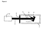
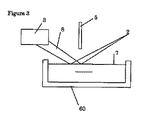
- プラズマ形成部位を囲む容器と、前記容器へまたは前記容器から光放射を伝達する光デバイスと、前記光デバイスと前記プラズマ形成部位源との間の光路に配置され、前記光デバイスと前記プラズマ形成部位との間で前記光放射を反射するリフレクタと、溶融金属を収容する槽とを含むプラズマ源を含み、
前記リフレクタは、前記槽内の前記溶融金属に前記リフレクタを接触させることによって形成される反射面を備える、
リソグラフィ装置。 - 前記プラズマ形成部位の見通し線内に配置され、前記光デバイスをデブリから保護するシールドをさらに含む、請求項1に記載のリソグラフィ装置。
- 前記溶融金属は、スズ溶融物を含む、請求項1または2に記載のリソグラフィ装置。
- 前記プラズマ形成部位は、スズまたはリチウムを含む、請求項1〜3のいずれか一項に記載のリソグラフィ装置。
- 前記光デバイスは、前記プラズマ形成部位の放電領域においてプラズマを生成するレーザデバイスである、請求項1〜4のいずれか一項に記載のリソグラフィ装置。
- 前記リフレクタは、重力方向に対して傾斜した角度において前記槽内に配置される、
請求項1〜5のいずれか一項に記載のリソグラフィ装置。 - 前記槽の中で前記リフレクタが回転可能に構成されている、請求項1〜6のいずれか一項に記載のリソグラフィ装置。
- 前記リフレクタの前記反射面は、前記光放射の集束力を与えるために湾曲される、請求項1〜7のいずれか一項に記載のリソグラフィ装置。
- 前記リフレクタは、金またはモリブデンを含む層を有する、請求項1〜8のいずれか一項に記載のリソグラフィ装置。
- 水素ガスを供給するインレットと、
前記リフレクタを加熱するヒータと、
をさらに有する請求項1〜9のいずれか一項に記載のリソグラフィ装置。 - 水素ラジカルガスを供給するインレットをさらに有する、請求項1〜9のいずれか一項に記載のリソグラフィ装置。
- プラズマ形成部位を囲む容器と、
前記容器へまたは前記容器から放射を伝達する光デバイスと、
前記光デバイスと前記プラズマ形成部位との間の光路に配置され、前記光デバイスと前記プラズマ形成部位との間で前記放射を反射する、リフレクタと、
溶融金属を収容する槽と、
を含み、
前記リフレクタは、前記槽内の前記溶融金属に前記リフレクタを接触させることによって形成される反射面を備える、プラズマ源。
Applications Claiming Priority (3)
| Application Number | Priority Date | Filing Date | Title |
|---|---|---|---|
| US6438508P | 2008-03-03 | 2008-03-03 | |
| US61/064,385 | 2008-03-03 | ||
| PCT/NL2009/050096 WO2009110793A1 (en) | 2008-03-03 | 2009-03-03 | Lithographic apparatus, plasma source, and reflecting method |
Publications (2)
| Publication Number | Publication Date |
|---|---|
| JP2011513987A JP2011513987A (ja) | 2011-04-28 |
| JP5583033B2 true JP5583033B2 (ja) | 2014-09-03 |
Family
ID=40718751
Family Applications (1)
| Application Number | Title | Priority Date | Filing Date |
|---|---|---|---|
| JP2010549598A Expired - Fee Related JP5583033B2 (ja) | 2008-03-03 | 2009-03-03 | リソグラフィ装置およびプラズマ源 |
Country Status (7)
| Country | Link |
|---|---|
| US (1) | US8593617B2 (ja) |
| JP (1) | JP5583033B2 (ja) |
| KR (1) | KR101591686B1 (ja) |
| CN (1) | CN101971100B (ja) |
| NL (1) | NL1036613A1 (ja) |
| TW (1) | TWI420251B (ja) |
| WO (1) | WO2009110793A1 (ja) |
Families Citing this family (13)
| Publication number | Priority date | Publication date | Assignee | Title |
|---|---|---|---|---|
| JP5511705B2 (ja) * | 2011-02-10 | 2014-06-04 | ギガフォトン株式会社 | ターゲット供給装置及び極端紫外光生成装置 |
| WO2013186008A1 (en) * | 2012-06-14 | 2013-12-19 | University College Dublin, National University Of Ireland, Dublin | A self-cleaning optical system |
| JP6182601B2 (ja) | 2012-06-22 | 2017-08-16 | エーエスエムエル ネザーランズ ビー.ブイ. | 放射源及びリソグラフィ装置 |
| CN103837913B (zh) * | 2012-11-26 | 2016-05-04 | 中国科学院理化技术研究所 | 反光镜及其制作工艺 |
| US9429858B2 (en) | 2013-09-24 | 2016-08-30 | Taiwan Semiconductor Manufacturing Co., Ltd. | Rotary EUV collector |
| WO2016174752A1 (ja) | 2015-04-28 | 2016-11-03 | ギガフォトン株式会社 | チャンバ装置、ターゲット生成方法および極端紫外光生成装置 |
| US20170311429A1 (en) * | 2016-04-25 | 2017-10-26 | Asml Netherlands B.V. | Reducing the effect of plasma on an object in an extreme ultraviolet light source |
| JP6763959B2 (ja) | 2016-09-30 | 2020-09-30 | ギガフォトン株式会社 | チャンバ装置、ターゲット生成方法および極端紫外光生成装置 |
| US10775700B2 (en) * | 2018-08-14 | 2020-09-15 | Taiwan Semiconductor Manufacturing Co., Ltd. | Lithography system and method for exposing wafer |
| CN109215818B (zh) * | 2018-08-22 | 2022-04-15 | 中国科学院合肥物质科学研究院 | 用于聚变堆等离子体与材料相互作用测试平台的限制器 |
| US11340531B2 (en) * | 2020-07-10 | 2022-05-24 | Taiwan Semiconductor Manufacturing Company, Ltd. | Target control in extreme ultraviolet lithography systems using aberration of reflection image |
| KR20230015672A (ko) | 2021-07-23 | 2023-01-31 | 주식회사 에프에스티 | 잔해 차폐 막 및 그 제조방법 |
| KR20230168383A (ko) | 2022-06-07 | 2023-12-14 | 주식회사 에프에스티 | 잔해 차폐 막 및 그 제조방법 |
Family Cites Families (12)
| Publication number | Priority date | Publication date | Assignee | Title |
|---|---|---|---|---|
| JPS55143502A (en) | 1979-04-25 | 1980-11-08 | Toshikatsu Omiya | Production of paraboloid-of-revolution mirror |
| JP4238390B2 (ja) * | 1998-02-27 | 2009-03-18 | 株式会社ニコン | 照明装置、該照明装置を備えた露光装置および該露光装置を用いて半導体デバイスを製造する方法 |
| JP2004140390A (ja) | 2003-12-01 | 2004-05-13 | Canon Inc | 照明光学系、露光装置及びデバイス製造方法 |
| US7109503B1 (en) | 2005-02-25 | 2006-09-19 | Cymer, Inc. | Systems for protecting internal components of an EUV light source from plasma-generated debris |
| US7482609B2 (en) * | 2005-02-28 | 2009-01-27 | Cymer, Inc. | LPP EUV light source drive laser system |
| US7233010B2 (en) * | 2005-05-20 | 2007-06-19 | Asml Netherlands B.V. | Radiation system and lithographic apparatus |
| ATE430369T1 (de) * | 2005-11-02 | 2009-05-15 | Univ Dublin | Spiegel für hochleistungs-euv-lampensystem |
| US7468521B2 (en) * | 2005-12-28 | 2008-12-23 | Asml Netherlands B.V. | Lithographic apparatus and device manufacturing method |
| JP4702107B2 (ja) | 2006-03-03 | 2011-06-15 | 株式会社日立製作所 | 生体光計測装置 |
| DE102006034755A1 (de) | 2006-07-24 | 2008-01-31 | Carl Zeiss Smt Ag | Optische Vorrichtung sowie Verfahren zur Korrektur bzw. Verbesserung des Abbildungsverhaltens einer optischen Vorrichtung |
| US7724349B2 (en) | 2007-05-02 | 2010-05-25 | Asml Netherlands B.V. | Device arranged to measure a quantity relating to radiation and lithographic apparatus |
| US7839482B2 (en) | 2007-05-21 | 2010-11-23 | Asml Netherlands B.V. | Assembly comprising a radiation source, a reflector and a contaminant barrier |
-
2009
- 2009-02-23 NL NL1036613A patent/NL1036613A1/nl active Search and Examination
- 2009-03-03 WO PCT/NL2009/050096 patent/WO2009110793A1/en active Application Filing
- 2009-03-03 JP JP2010549598A patent/JP5583033B2/ja not_active Expired - Fee Related
- 2009-03-03 TW TW098106870A patent/TWI420251B/zh not_active IP Right Cessation
- 2009-03-03 KR KR1020107022051A patent/KR101591686B1/ko not_active IP Right Cessation
- 2009-03-03 US US12/920,417 patent/US8593617B2/en not_active Expired - Fee Related
- 2009-03-03 CN CN200980107377.4A patent/CN101971100B/zh not_active Expired - Fee Related
Also Published As
| Publication number | Publication date |
|---|---|
| JP2011513987A (ja) | 2011-04-28 |
| TW200942992A (en) | 2009-10-16 |
| US20110007292A1 (en) | 2011-01-13 |
| TWI420251B (zh) | 2013-12-21 |
| NL1036613A1 (nl) | 2009-09-07 |
| WO2009110793A1 (en) | 2009-09-11 |
| CN101971100B (zh) | 2013-10-16 |
| CN101971100A (zh) | 2011-02-09 |
| KR20100124308A (ko) | 2010-11-26 |
| KR101591686B1 (ko) | 2016-02-04 |
| US8593617B2 (en) | 2013-11-26 |
Similar Documents
| Publication | Publication Date | Title |
|---|---|---|
| JP5583033B2 (ja) | リソグラフィ装置およびプラズマ源 | |
| JP4335868B2 (ja) | リソグラフィ装置、照明系及びデブリ捕捉システム | |
| JP5191541B2 (ja) | 極端紫外線を生成するモジュールおよび方法、並びにリソグラフィ投影装置 | |
| JP4369420B2 (ja) | デブリ粒子を抑制するための放射線源装置、リソグラフィ装置、照明システム、および方法 | |
| JP5732525B2 (ja) | コレクタミラーアセンブリおよび極端紫外線放射の生成方法 | |
| JP4799620B2 (ja) | 放射システムおよびリソグラフィ装置 | |
| US9363879B2 (en) | Module and method for producing extreme ultraviolet radiation | |
| JP5070264B2 (ja) | ソースモジュール、放射ソースおよびリソグラフィ装置 | |
| JP2011530819A (ja) | 放射源、リソグラフィ装置、およびデバイス製造方法 | |
| JP4875754B2 (ja) | 回転電極を備える放射源、および放射源を備えるリソグラフィ装置 | |
| JP6291477B2 (ja) | リソグラフィ装置用の汚染トラップ | |
| JP2013524525A (ja) | Euv放射源およびeuv放射生成方法 | |
| JP4875753B2 (ja) | EUV源におけるデブリ抑制用影つけ電極(shadowingelectrode) | |
| KR101790074B1 (ko) | 방사선 소스, 리소그래피 장치 및 디바이스 제조 방법 | |
| US8319200B2 (en) | Radiation source, lithographic apparatus and device manufacturing method | |
| JP4778542B2 (ja) | リソグラフィ装置、放射システム、デバイス製造方法、及び放射生成方法 | |
| JP4814922B2 (ja) | リソグラフィ装置の光エレメントの保護方法、リソグラフィ装置、およびデバイス製造方法 | |
| JP2010045355A (ja) | 放射源、リソグラフィ装置、および、デバイス製造方法 | |
| JP2011513967A (ja) | 放射を発生させるように構成されたデバイス、リソグラフィ装置、およびデバイス製造方法 | |
| JP2010522953A (ja) | 電磁放射を発生させるための放射源及び電磁放射の発生方法 |
Legal Events
| Date | Code | Title | Description |
|---|---|---|---|
| A621 | Written request for application examination |
Free format text: JAPANESE INTERMEDIATE CODE: A621 Effective date: 20120301 |
|
| A977 | Report on retrieval |
Free format text: JAPANESE INTERMEDIATE CODE: A971007 Effective date: 20130118 |
|
| A131 | Notification of reasons for refusal |
Free format text: JAPANESE INTERMEDIATE CODE: A131 Effective date: 20130123 |
|
| A131 | Notification of reasons for refusal |
Free format text: JAPANESE INTERMEDIATE CODE: A131 Effective date: 20131028 |
|
| A521 | Request for written amendment filed |
Free format text: JAPANESE INTERMEDIATE CODE: A523 Effective date: 20140116 |
|
| TRDD | Decision of grant or rejection written | ||
| A01 | Written decision to grant a patent or to grant a registration (utility model) |
Free format text: JAPANESE INTERMEDIATE CODE: A01 Effective date: 20140619 |
|
| A61 | First payment of annual fees (during grant procedure) |
Free format text: JAPANESE INTERMEDIATE CODE: A61 Effective date: 20140715 |
|
| R150 | Certificate of patent or registration of utility model |
Ref document number: 5583033 Country of ref document: JP Free format text: JAPANESE INTERMEDIATE CODE: R150 |
|
| LAPS | Cancellation because of no payment of annual fees |