JP5580045B2 - Silicon carbide and related wide band gap transistors on semi-insulating epitaxy - Google Patents
Silicon carbide and related wide band gap transistors on semi-insulating epitaxy Download PDFInfo
- Publication number
- JP5580045B2 JP5580045B2 JP2009516677A JP2009516677A JP5580045B2 JP 5580045 B2 JP5580045 B2 JP 5580045B2 JP 2009516677 A JP2009516677 A JP 2009516677A JP 2009516677 A JP2009516677 A JP 2009516677A JP 5580045 B2 JP5580045 B2 JP 5580045B2
- Authority
- JP
- Japan
- Prior art keywords
- epitaxial layer
- boron
- substrate
- region
- semi
- Prior art date
- Legal status (The legal status is an assumption and is not a legal conclusion. Google has not performed a legal analysis and makes no representation as to the accuracy of the status listed.)
- Expired - Fee Related
Links
- 229910010271 silicon carbide Inorganic materials 0.000 title claims description 55
- HBMJWWWQQXIZIP-UHFFFAOYSA-N silicon carbide Chemical compound [Si+]#[C-] HBMJWWWQQXIZIP-UHFFFAOYSA-N 0.000 title claims description 52
- 238000000407 epitaxy Methods 0.000 title description 4
- 229910052796 boron Inorganic materials 0.000 claims description 113
- ZOXJGFHDIHLPTG-UHFFFAOYSA-N Boron Chemical compound [B] ZOXJGFHDIHLPTG-UHFFFAOYSA-N 0.000 claims description 103
- 239000000758 substrate Substances 0.000 claims description 74
- 238000000034 method Methods 0.000 claims description 31
- 238000002513 implantation Methods 0.000 claims description 28
- 239000000463 material Substances 0.000 claims description 23
- 238000009792 diffusion process Methods 0.000 claims description 14
- -1 boron ions Chemical class 0.000 claims description 11
- 239000007943 implant Substances 0.000 claims description 7
- 238000000137 annealing Methods 0.000 claims description 5
- 238000005530 etching Methods 0.000 claims description 5
- 238000004519 manufacturing process Methods 0.000 claims description 3
- 239000007790 solid phase Substances 0.000 claims 1
- 239000010410 layer Substances 0.000 description 155
- 239000004065 semiconductor Substances 0.000 description 15
- 230000015572 biosynthetic process Effects 0.000 description 11
- VYPSYNLAJGMNEJ-UHFFFAOYSA-N Silicium dioxide Chemical compound O=[Si]=O VYPSYNLAJGMNEJ-UHFFFAOYSA-N 0.000 description 4
- 238000002955 isolation Methods 0.000 description 4
- 239000007787 solid Substances 0.000 description 4
- 239000002019 doping agent Substances 0.000 description 3
- IJGRMHOSHXDMSA-UHFFFAOYSA-N Atomic nitrogen Chemical compound N#N IJGRMHOSHXDMSA-UHFFFAOYSA-N 0.000 description 2
- 239000013078 crystal Substances 0.000 description 2
- 230000007547 defect Effects 0.000 description 2
- 230000005669 field effect Effects 0.000 description 2
- 238000004377 microelectronic Methods 0.000 description 2
- 238000012986 modification Methods 0.000 description 2
- 230000004048 modification Effects 0.000 description 2
- 235000012239 silicon dioxide Nutrition 0.000 description 2
- 239000000377 silicon dioxide Substances 0.000 description 2
- 229910004298 SiO 2 Inorganic materials 0.000 description 1
- XUIMIQQOPSSXEZ-UHFFFAOYSA-N Silicon Chemical group [Si] XUIMIQQOPSSXEZ-UHFFFAOYSA-N 0.000 description 1
- 230000003321 amplification Effects 0.000 description 1
- 230000005540 biological transmission Effects 0.000 description 1
- 238000004891 communication Methods 0.000 description 1
- 238000005094 computer simulation Methods 0.000 description 1
- 230000003750 conditioning effect Effects 0.000 description 1
- 230000006735 deficit Effects 0.000 description 1
- 238000013461 design Methods 0.000 description 1
- 238000010586 diagram Methods 0.000 description 1
- 238000005516 engineering process Methods 0.000 description 1
- 239000010408 film Substances 0.000 description 1
- 239000012212 insulator Substances 0.000 description 1
- 229910052757 nitrogen Inorganic materials 0.000 description 1
- 238000003199 nucleic acid amplification method Methods 0.000 description 1
- 238000005192 partition Methods 0.000 description 1
- 238000003672 processing method Methods 0.000 description 1
- 229910052710 silicon Inorganic materials 0.000 description 1
- 239000010703 silicon Substances 0.000 description 1
- 238000006467 substitution reaction Methods 0.000 description 1
- 239000002344 surface layer Substances 0.000 description 1
- 239000010409 thin film Substances 0.000 description 1
- 230000007704 transition Effects 0.000 description 1
- 239000002918 waste heat Substances 0.000 description 1
Images


Classifications
-
- H—ELECTRICITY
- H01—ELECTRIC ELEMENTS
- H01L—SEMICONDUCTOR DEVICES NOT COVERED BY CLASS H10
- H01L29/00—Semiconductor devices adapted for rectifying, amplifying, oscillating or switching, or capacitors or resistors with at least one potential-jump barrier or surface barrier, e.g. PN junction depletion layer or carrier concentration layer; Details of semiconductor bodies or of electrodes thereof ; Multistep manufacturing processes therefor
- H01L29/02—Semiconductor bodies ; Multistep manufacturing processes therefor
- H01L29/12—Semiconductor bodies ; Multistep manufacturing processes therefor characterised by the materials of which they are formed
- H01L29/15—Structures with periodic or quasi periodic potential variation, e.g. multiple quantum wells, superlattices
-
- H—ELECTRICITY
- H01—ELECTRIC ELEMENTS
- H01L—SEMICONDUCTOR DEVICES NOT COVERED BY CLASS H10
- H01L21/00—Processes or apparatus adapted for the manufacture or treatment of semiconductor or solid state devices or of parts thereof
- H01L21/70—Manufacture or treatment of devices consisting of a plurality of solid state components formed in or on a common substrate or of parts thereof; Manufacture of integrated circuit devices or of parts thereof
- H01L21/77—Manufacture or treatment of devices consisting of a plurality of solid state components or integrated circuits formed in, or on, a common substrate
- H01L21/78—Manufacture or treatment of devices consisting of a plurality of solid state components or integrated circuits formed in, or on, a common substrate with subsequent division of the substrate into plural individual devices
- H01L21/82—Manufacture or treatment of devices consisting of a plurality of solid state components or integrated circuits formed in, or on, a common substrate with subsequent division of the substrate into plural individual devices to produce devices, e.g. integrated circuits, each consisting of a plurality of components
- H01L21/8213—Manufacture or treatment of devices consisting of a plurality of solid state components or integrated circuits formed in, or on, a common substrate with subsequent division of the substrate into plural individual devices to produce devices, e.g. integrated circuits, each consisting of a plurality of components the substrate being a semiconductor, using SiC technology
-
- H—ELECTRICITY
- H01—ELECTRIC ELEMENTS
- H01L—SEMICONDUCTOR DEVICES NOT COVERED BY CLASS H10
- H01L29/00—Semiconductor devices adapted for rectifying, amplifying, oscillating or switching, or capacitors or resistors with at least one potential-jump barrier or surface barrier, e.g. PN junction depletion layer or carrier concentration layer; Details of semiconductor bodies or of electrodes thereof ; Multistep manufacturing processes therefor
- H01L29/02—Semiconductor bodies ; Multistep manufacturing processes therefor
- H01L29/12—Semiconductor bodies ; Multistep manufacturing processes therefor characterised by the materials of which they are formed
- H01L29/16—Semiconductor bodies ; Multistep manufacturing processes therefor characterised by the materials of which they are formed including, apart from doping materials or other impurities, only elements of Group IV of the Periodic System
- H01L29/1608—Silicon carbide
-
- H—ELECTRICITY
- H01—ELECTRIC ELEMENTS
- H01L—SEMICONDUCTOR DEVICES NOT COVERED BY CLASS H10
- H01L29/00—Semiconductor devices adapted for rectifying, amplifying, oscillating or switching, or capacitors or resistors with at least one potential-jump barrier or surface barrier, e.g. PN junction depletion layer or carrier concentration layer; Details of semiconductor bodies or of electrodes thereof ; Multistep manufacturing processes therefor
- H01L29/66—Types of semiconductor device ; Multistep manufacturing processes therefor
- H01L29/66007—Multistep manufacturing processes
- H01L29/66053—Multistep manufacturing processes of devices having a semiconductor body comprising crystalline silicon carbide
- H01L29/66068—Multistep manufacturing processes of devices having a semiconductor body comprising crystalline silicon carbide the devices being controllable only by the electric current supplied or the electric potential applied, to an electrode which does not carry the current to be rectified, amplified or switched, e.g. three-terminal devices
-
- H—ELECTRICITY
- H01—ELECTRIC ELEMENTS
- H01L—SEMICONDUCTOR DEVICES NOT COVERED BY CLASS H10
- H01L29/00—Semiconductor devices adapted for rectifying, amplifying, oscillating or switching, or capacitors or resistors with at least one potential-jump barrier or surface barrier, e.g. PN junction depletion layer or carrier concentration layer; Details of semiconductor bodies or of electrodes thereof ; Multistep manufacturing processes therefor
- H01L29/66—Types of semiconductor device ; Multistep manufacturing processes therefor
- H01L29/68—Types of semiconductor device ; Multistep manufacturing processes therefor controllable by only the electric current supplied, or only the electric potential applied, to an electrode which does not carry the current to be rectified, amplified or switched
- H01L29/76—Unipolar devices, e.g. field effect transistors
- H01L29/772—Field effect transistors
- H01L29/78—Field effect transistors with field effect produced by an insulated gate
Description
本発明は、全般的には半導体デバイスおよび二次加工方法、およびより具体的には炭化ケイ素半絶縁層を採用する半導体デバイスに関する。 The present invention relates generally to semiconductor devices and secondary processing methods, and more specifically to semiconductor devices employing silicon carbide semi-insulating layers.
(関連明細書の参照)
本明細書は、その全内容を参照文献として援用する2006年6月19日に出願された米国仮特許出願番号第60/805,139号に基づき、且つこれに優先して請求する。
(Refer to related statement)
This specification is based on and preempts US Provisional Patent Application No. 60 / 805,139, filed Jun. 19, 2006, the entire contents of which are incorporated by reference.
本発明の1つの態様は、半絶縁エピタキシャル層を生成する方法を提供することである。方法は、基板の表面上あるいは第1のエピタキシャル層の表面上にホウ素注入領域を形成するためにホウ素イオンを基板あるいは基板上に形成された第1のエピタキシャル層に注入すること、および半絶縁エピタキシャル層を形成するために基板のホウ素注入領域上あるいは第1のエピタキシャル層のホウ素注入領域上に第2のエピタキシャル層を成長させることを含む。 One aspect of the present invention is to provide a method for producing a semi-insulating epitaxial layer. The method includes implanting boron ions into a substrate or a first epitaxial layer formed on the substrate to form a boron implanted region on the surface of the substrate or on the surface of the first epitaxial layer, and semi-insulating epitaxial. Growing a second epitaxial layer on the boron implanted region of the substrate or on the boron implanted region of the first epitaxial layer to form a layer.
本発明の他の態様はマイクロエレクトロニクスデバイスを提供することである。デバイスは基板、基板上に形成された半絶縁炭化ケイ素エピタキシャル層を含む。半絶縁炭化ケイ素エピタキシャル層はホウ素およびホウ素関連D−センター欠損を含む。マイクロエレクトロニクスデバイスは、半絶縁炭化ケイ素層上に形成された第1の半導体デバイスも含む。半絶縁エピタキシャル炭化ケイ素層は、基板の表面上あるいは第1のエピタキシャル層の表面上にホウ素注入領域を形成するために基板あるいは基板上に形成された第1のエピタキシャル層にホウ素イオンを注入すること、および基板のホウ素注入領域上あるいは第1のエピタキシャル層のホウ素注入領域上に第2のエピタキシャル層を成長させることにより形成される。 Another aspect of the present invention is to provide a microelectronic device. The device includes a substrate, a semi-insulating silicon carbide epitaxial layer formed on the substrate. The semi-insulating silicon carbide epitaxial layer includes boron and boron related D-center defects. The microelectronic device also includes a first semiconductor device formed on the semi-insulating silicon carbide layer. The semi-insulating epitaxial silicon carbide layer implants boron ions into the substrate or the first epitaxial layer formed on the substrate to form a boron implantation region on the surface of the substrate or on the surface of the first epitaxial layer. And growing a second epitaxial layer on the boron implantation region of the substrate or on the boron implantation region of the first epitaxial layer.
図1は、本発明の1つの実施形態による、SiC MOSFETデバイスの断面の模式図である。デバイス10は、その上にエピタキシャル成長などにより半絶縁炭化ケイ素エピタキシャル層13を形成する基板12(例:n+6H炭化ケイ素)を含む。p−炭化ケイ素層14は半絶縁(SI)炭化ケイ素エピタキシャル層13上に形成される。p−炭化ケイ素層14は、n型ドリフト領域などの段階的注入領域17を含む。
FIG. 1 is a schematic diagram of a cross section of a SiC MOSFET device, according to one embodiment of the present invention. The
たとえばコンタクト領域20を伴うn+ソース領域、n+ソースウェル21およびp+ボディコンタクト22などを含むソース/ボディS、さらにはたとえばコンタクト領域15を伴うn+ドレイン領域およびn+ドレインウェル16を含むドレインDが、p−炭化ケイ素層14上に形成される。p−炭化ケイ素層14上には、ゲートおよびコンタクト領域19に沿って二酸化ケイ素層18も形成される。
For example, an n + source region with
1つの実施形態においては、MOSFETデバイス10の全ての層はエピタキシャル成長する。1つの実施形態においては、以下の段落で詳細に記載する多数の方法のうち1つによってSI SiC層13が形成される。
In one embodiment, all layers of
図2は、本発明の1つの実施形態による、同じSiCチップ40上に形成された第1の半導体デバイス44および第2の半導体デバイス49の断面の模式図である。図2に示すように、SiCチップ40はn+基板などの基板41、エピタキシャル層などのSI層42を含む。たとえばデバイスの形成、第1の半導体デバイス44と第2の半導体デバイス49の分離(例:電気的分離)などのために、必要に応じて任意の浅いトレンチ分離(STI)43が提供される。
FIG. 2 is a schematic cross-sectional view of a
1つの実施形態においては、第1の半導体デバイス44は垂直バイポーラ接合トランジスタ(BJT)であり、且つ第2の半導体デバイス49は垂直接合電界効果トランジスタ(JFET)である。BJTデバイス44はn−コレクター45,n+サブコレクター46,p−ベース47およびn+エミッタ48などの多様な形態を含む。垂直JFET49はソース層50などの多様な形態を含む。ソース層50はたとえばn+層などとすることができる。垂直JFET49はp+層とすることのできるゲート領域51および52、およびn+層とすることのできるドレイン領域53も含む。コンタクト54はドレイン領域53内に提供される。
In one embodiment, the
図2のデバイス44および49はそれぞれ単にSI層42上に形成することのできるデバイスの例となることを意図している。SIエピタキシーにより、これらの垂直電源デバイスは、「スマートパワーIC」としても知られる、SiCにおいて複雑な多機能(例:電源調節、制御、増幅)モノリシック回路の基盤を形成する、水平電源デバイスあるいは水平制御サーキットリーと同じチップ上に集積することが可能である。多様なデバイスの詳細な説明は、その内容が本明細書に参照文献として援用される、「高速、高出力用途向けの半絶縁エピタキシー上の炭化ケイ素および関連ワイドバンドギャップトランジスタ」という名称のCasadyらの米国特許第7,009,209号において認めることができる。
第1に、デバイス間の電気的分離を達成することができる。より品質が高く安価な伝導性4H SiC基板上で半絶縁エピタキシャル層を成長させることにより、技術的性能も入手しやすさも高まる。第2に、シリコン・オン・インシュレータ(SOI)ではなくSiCを用いると、半絶縁SiCエピタキシャル層の熱伝導性がSOIで使用されるSiO2の熱伝導性をさらに上回るので、高出力密度集積回路がより良好に達成される。したがって、廃熱除去効率がはるかに高くなる。たとえば、熱伝導性の比率に基づけば、SI SiCバッファ層は、SOIで用いられる典型的な二酸化ケイ素バッファ層と比較して、単位面積あたり231倍の熱を伝導することができる。 First, electrical isolation between devices can be achieved. By growing a semi-insulating epitaxial layer on a higher quality and cheaper conductive 4H SiC substrate, technical performance and availability are also increased. Second, the use of SiC rather than silicon-on-insulator (SOI) increases the thermal conductivity of the semi-insulating SiC epitaxial layer further than the thermal conductivity of SiO 2 used in SOI, resulting in a high power density integrated circuit. Is better achieved. Therefore, the waste heat removal efficiency is much higher. For example, based on the thermal conductivity ratio, the SI SiC buffer layer can conduct 231 times more heat per unit area compared to a typical silicon dioxide buffer layer used in SOI.
本明細書の以下の段落には、SI SiCエピタキシャルフィルムを成長させる多様な方法を記載する。1つの方法は、SiCエピタキシャル層の成長時に浅い窒素ドナーを補償するためにホウ素関連D−センターを用いることを含む。D−センターはSiCにおいて価電子帯よりも0.7eV上にあり、研究された全てのSiCポリタイプで検出されている。「点欠損」としても知られるホウ素関連D−センターは、SiC結晶におけるケイ素置換部位を占めるホウ素原子に関連する。 The following paragraphs of this specification describe various methods of growing SI SiC epitaxial films. One method involves using boron-related D-centers to compensate for shallow nitrogen donors during the growth of the SiC epitaxial layer. The D-center is 0.7 eV above the valence band in SiC and has been detected in all SiC polytypes studied. Boron-related D-centers, also known as “point deficits”, relate to boron atoms that occupy silicon substitution sites in SiC crystals.
炭化ケイ素の各ポリタイプ(例:6H SiCおよび4H SiC)は半導体デバイスにおいて異なる特性をもたらすことができるので、多様な用途に用いることができる。たとえば、6H SiCと4H SiCの違いの1つはこれらのポリタイプのバンドギャップであり、6H SiCのバンドギャップは約2.9eVであるのに対し、4H SiCでは約3.2eVである。これらのポリタイプ間の0.3eVの差によって、それぞれが異なる用途に典型的に適する。たとえば、4H SiCはより大きなバンドギャップを利用するために高電圧あるいは高出力用途に対して好ましいことが多いのに対し、6H SiCは、たとえば発光ダイオードにおいて一般に商業使用されることから、一部の用途に使用されるのに好ましい。本発明は全てのSiCポリタイプにおいて良好に作動することが観察されている。 Each polytype of silicon carbide (eg, 6H SiC and 4H SiC) can provide different properties in semiconductor devices and can therefore be used in a variety of applications. For example, one of the differences between 6H SiC and 4H SiC is the band gap of these polytypes, which is about 2.9 eV compared to about 3.2 eV for 4H SiC. The 0.3 eV difference between these polytypes is typically suitable for different applications. For example, 4H SiC is often preferred for high voltage or high power applications to take advantage of the larger bandgap, whereas 6H SiC is commonly used commercially, for example in light emitting diodes, so some Preferred for use in applications. The invention has been observed to work well with all SiC polytypes.
ホウ素関連D−センターを含む補償エピタキシャル層を形成するために、多くの異なる固形ホウ素源を用いることができる。固形ホウ素源は、固形ドーピングソース以外にも、基板、もう1つの隣接するエピタキシャル層、あるいはエピタキシャル層それ自体にあってもよい。1つの実施形態においては、ホウ素の補償エピタキシャル層への輸送はその拡散による。ホウ素の拡散およびこれによる所望のD−センター欠損の形成は、基板上あるいは基板上で始めに成長する隣接する伝導エピタキシャル層上での補償エピタキシャル層の成長時に発生する可能性がある。 Many different solid boron sources can be used to form a compensated epitaxial layer that includes boron-related D-centers. Besides the solid doping source, the solid boron source may be in the substrate, another adjacent epitaxial layer, or the epitaxial layer itself. In one embodiment, the transport of boron to the compensating epitaxial layer is due to its diffusion. Boron diffusion and thereby the formation of the desired D-center defect can occur during the growth of the compensation epitaxial layer on the substrate or on the adjacent conductive epitaxial layer that initially grows on the substrate.
拡散についての必須条件は、基板および/あるいは第1の伝導性エピタキシャル層の表面へのホウ素の注入である。注入した材料の結晶構造における損傷により、変則的に速いホウ素の拡散および高いD−センター形成効率を促進する。 A prerequisite for diffusion is the implantation of boron into the surface of the substrate and / or the first conductive epitaxial layer. Damage in the crystal structure of the implanted material promotes irregularly fast boron diffusion and high D-center formation efficiency.
1つの実施形態では、標的エピタキシャル層それ自体に直接ホウ素を注入する均一法を用いることもできる。他の実施形態では、隣接するSiC材料内でドーピングする固形ソースの不均一法を用いることもできる。始めにエピタキシャル層が成長し、その後ホウ素がその層に注入されるのであれば、ホウ素はこれに続く熱アニーリング段階で再分布してD−センターを形成するであろう。不均一なあるいは均一な実施形態のいずれかにより、炭化ケイ素のエピタキシャル成長半絶縁薄型フィルムを含むデバイスが生成する。 In one embodiment, a uniform method of implanting boron directly into the target epitaxial layer itself can be used. In other embodiments, a non-uniform method of solid source doping in adjacent SiC material may be used. If an epitaxial layer is first grown and then boron is implanted into the layer, the boron will redistribute in a subsequent thermal annealing step to form a D-center. Either a non-uniform or uniform embodiment produces a device comprising an epitaxially grown semi-insulating thin film of silicon carbide.
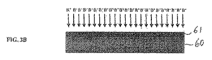
図3A〜3Cは、本発明の1つの実施形態による、半絶縁(SI)エピタキシャル層を形成するための各手順を描出する。この実施形態においては、基板をホウ素源として利用してもよい。始めに、図3Aに描出するように基板60を提供する。基板60は炭化ケイ素を含んでもよい。基板は、たとえばp型SiC基板などとすることができる。図3Bに描出するように、基板60の表面がホウ素イオンで衝撃されて基板60内にホウ素注入領域61が形成される。ホウ素注入領域61の形成後、ホウ素注入領域61上にエピタキシャル層を成長させる。1つの実施形態においては、エピタキシャル層の成長は約1,500℃〜1,700℃の温度、たとえば約1,600℃の温度で約1時間〜3時間の間、たとえば約1時間の間実施する。1つの実施形態においては、エピタキシャル層62はn型エピタキシャル層である。図3Cに示すように、エピタキシャル層62の成長時、ホウ素領域61内のホウ素がエピタキシャル層62に拡散して半絶縁エピタキシャル層62を形成する。ホウ素注入領域61はホウ素源として働き、またホウ素注入領域61内のホウ素が、ホウ素注入領域61上で成長するエピタキシャル層内に拡散する。ホウ素のエピタキシャル層62への拡散により、浅いドナーを補償するホウ素関連D−センターが形成される。成長エピタキシャル層62の表面近くの材料がn型であるとき、ホウ素注入基板とのインターフェースにより近いプロフィールより明白なp型への転位が判明する。 3A-3C depict steps for forming a semi-insulating (SI) epitaxial layer, according to one embodiment of the present invention. In this embodiment, the substrate may be used as a boron source. First, a substrate 60 is provided as depicted in FIG. 3A. The substrate 60 may include silicon carbide. The substrate can be, for example, a p-type SiC substrate. As depicted in FIG. 3B, the surface of the substrate 60 is bombarded with boron ions to form a boron implanted region 61 in the substrate 60. After forming the boron implantation region 61, an epitaxial layer is grown on the boron implantation region 61. In one embodiment, the epitaxial layer growth is performed at a temperature of about 1,500 ° C. to 1,700 ° C., for example, at a temperature of about 1,600 ° C., for about 1 hour to 3 hours, for example, about 1 hour. To do. In one embodiment, the epitaxial layer 62 is an n-type epitaxial layer. As shown in FIG. 3C, when the epitaxial layer 62 is grown, boron in the boron region 61 diffuses into the epitaxial layer 62 to form a semi-insulating epitaxial layer 62. The boron implantation region 61 serves as a boron source, and boron in the boron implantation region 61 diffuses into the epitaxial layer grown on the boron implantation region 61. The diffusion of boron into the epitaxial layer 62 forms boron-related D-centers that compensate for shallow donors. When the material near the surface of the grown epitaxial layer 62 is n-type, a clearer transition to p-type is found than a profile closer to the interface with the boron implanted substrate.
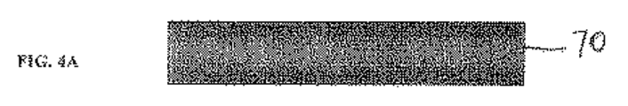
図4A〜4Dは、本発明の他の実施形態による、半絶縁(SI)エピタキシャル層を形成するための各手順を描出する。この実施形態においては、エピタキシャル層が基板上に形成され、すなわち基板に隣接するエピタキシャル層をホウ素源として使用してもよい。図4Aに描出するように、基板70が提供される。基板70は炭化ケイ素を含んでもよい。基板はあらゆる種類、たとえばp型SiC基板などとすることができる。図4Bに描出するように、第1のエピタキシャル層71を基板70上に形成する。1つの実施形態においては、第1のエピタキシャル層71はn型エピタキシャル層である。第1のエピタキシャル層71の形成後、図4Cに描出するように、第1のエピタキシャル層71の表面はホウ素イオンで衝撃され、第1のエピタキシャル層71内にホウ素注入領域72が形成される。ホウ素注入領域72の形成後、ホウ素注入領域72上に第2のエピタキシャル層74を成長させる。1つの実施形態においては、第2のエピタキシャル層74の成長は約1,500℃〜1,700℃の温度、たとえば約1,600℃の温度で約1時間〜3時間の間、たとえば約1時間の間実施する。1つの実施形態においては、第2のエピタキシャル層74はn型エピタキシャル層である。図4Dに示すように、第2のエピタキシャル層74の成長時、ホウ素領域72内のホウ素が第1のエピタキシャル層71に拡散して半絶縁層73を形成し、また第2のエピタキシャル層74内に拡散して半絶縁エピタキシャル層74を形成する。ホウ素注入領域72はホウ素源として作用し且つ第1および第2のエピタキシャル層内に拡散する。ホウ素の第1および第2のエピタキシャル層71、74への拡散により、第1のエピタキシャル層の中にも第2のエピタキシャル層の中にもホウ素関連D−センターが形成される。その結果は、ホウ素注入領域72のそれぞれ下および上におけるSI層73および74の形成である。
4A-4D depict steps for forming a semi-insulating (SI) epitaxial layer according to another embodiment of the present invention. In this embodiment, an epitaxial layer is formed on the substrate, i.e., an epitaxial layer adjacent to the substrate may be used as the boron source. As depicted in FIG. 4A, a substrate 70 is provided. The substrate 70 may include silicon carbide. The substrate can be any kind, such as a p-type SiC substrate. A
図5A〜5Dは、本発明の他の実施形態による、半絶縁(SI)エピタキシャル層を形成するための各手順を描出する。図5A〜5Dは、図3A〜3Cおよび4A〜4Dに描出した実施形態の均一な代替法である実施形態を例示する。この実施形態においては、図4A〜4Dに描出された実施形態と同様に、基板上に形成されたエピタキシャル層、すなわち基板に隣接するエピタキシャル層をホウ素源として使用してもよい。図5Aに描出するように、基板80が提供される。基板80は炭化ケイ素を含んでもよい。基板はあらゆる種類、たとえばp型SiC基板などとすることができる。図5Bに描出するように、エピタキシャル層81を基板80上に形成する。1つの実施形態においては、エピタキシャル層81はn型エピタキシャル層である。第1のエピタキシャル層81の形成後、図5Cに描出するように、エピタキシャル層81の表面はホウ素イオンで衝撃されてエピタキシャル層81内にホウ素注入領域82が形成される。1つの実施形態においては、エピタキシャル層の成長は約1,500〜1,700℃の温度、たとえば約1,600℃の温度で約1時間〜3時間の間、たとえば約1時間の間実施する。図5Dに示すように、ホウ素領域82内のホウ素がエピタキシャル層81に拡散して半絶縁層83を形成する。ホウ素注入領域82はホウ素源として作用し且つ基板80上に形成されたエピタキシャル層81内に拡散する。ホウ素のエピタキシャル層への拡散は、エピタキシャル層81内にホウ素関連D−センターを形成してSI層83を得る。SI層83を形成した後、たとえば技術上既知である何らかのエッチング法を用いるなどして、残ったホウ素注入領域82を除去することができる。得られたSI層は、下層の基板よりも高度にドーピングされたp型でなければならないといわれるp型であると規定される。
5A-5D depict steps for forming a semi-insulating (SI) epitaxial layer according to another embodiment of the present invention. 5A-5D illustrate an embodiment that is a uniform alternative to the embodiment depicted in FIGS. 3A-3C and 4A-4D. In this embodiment, as in the embodiment depicted in FIGS. 4A-4D, an epitaxial layer formed on the substrate, ie, an epitaxial layer adjacent to the substrate, may be used as the boron source. As depicted in FIG. 5A, a
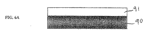
図6A〜6Dは、本発明の他の実施形態による、半絶縁(SI)エピタキシャル層を形成するための各手順を描出する。図6A〜6Dは図5A〜5Dに例示される方法の変法である実施形態を例示する。この実施形態においては、図5A〜5Dに描出された実施形態と同様に、基板上に形成されたエピタキシャル層、すなわち基板に隣接するエピタキシャル層をホウ素源として使用してもよい。しかし、この実施形態においてはマスク材料をエピタキシャル層の表面に適用する。具体的には、図6Aに描出するように基板90が提供される。基板90は炭化ケイ素を含んでもよい。基板90はあらゆる種類、たとえばn+型SiC基板などとすることができる。図6Aに描出するように、エピタキシャル層91を基板90上に形成する。1つの実施形態においては、エピタキシャル層91はn型エピタキシャル層である。第1のエピタキシャル層91の形成後、エピタキシャル層91の表面上にマスク領域および非マスク領域を形成するよう、エピタキシャル層91の表面にマスク材料92を適用する。マスク材料92をエピタキシャル層91の表面上に適用した後、図6Bに描出するように、たとえばエピタキシャル層91の非マスク(非保護)領域をエッチングすることなどにより、トレンチ93を形成する。トレンチ93を形成した後、その上にマスク材料92が蒸着されたエピタキシャル層91の表面をホウ素イオンで衝撃する。マスク材料92は、トレンチ93を形成するための選択的エッチングのためのマスクであるだけでなく、下層にあるエピタキシャル層91のマスク領域の注入を防止するためにも選択される。このようにして、マスク材料92はエピタキシャル層の選択的領域にドーピング材料を注入するための「ドーパントマスク」として用いることもできる。しかし、マスク材料92がドーパントマスクでない場合、マスク材料92を除去し、ドーパントマスクとして適した他のマスク材料をエピタキシャル層91の表面に適用することができる。ホウ素イオンは、トレンチ93の底面およびトレンチ93の側面を含むエピタキシャル層91の非保護領域に衝突する。その結果、図6Cに描出するように、エピタキシャル層91のトレンチ93内にホウ素注入領域94が形成される。ホウ素注入領域94を形成した後、図6Dに示すようにマスク領域94を取り除き、高温アニーリング工程を適用してホウ素をエピタキシャル層91により深く拡散させる。1つの実施形態においては、アニーリング工程は約1500℃から約1700℃の温度で約1時間から約3時間の間実施する。1つの実施例においては、アニーリング工程は約1,600℃の温度で約1時間の間実施する。一方、ホウ素のエピタキシャル層91への拡散により、D−センターが生成されて半絶縁エピタキシャル層95が作成される。トレンチ93の側壁におけるホウ素の注入は、トレンチにおける注入に伴う現象であり、トレンチ93によって形成されるチャンネルへのホウ素の拡散を支援する。上述の方法を用いた実施例は、その全内容を本明細書に参照文献として援用する「選択的エピタキシーあるいは選択的注入の使用による炭化ケイ素における自己配列トランジスタおよびダイオードトポロジー」という名称のCasadyらの米国特許第6,767,783号中に認めることができる。チャンネルのサイズは、数μm単位であるホウ素の予測拡散長およびホウ素関連D−センターの生成範囲と一致しなければならない。
6A-6D depict steps for forming a semi-insulating (SI) epitaxial layer according to another embodiment of the present invention. 6A-6D illustrate an embodiment that is a variation of the method illustrated in FIGS. 5A-5D. In this embodiment, similar to the embodiment depicted in FIGS. 5A-5D, an epitaxial layer formed on the substrate, ie, an epitaxial layer adjacent to the substrate, may be used as the boron source. However, in this embodiment, the mask material is applied to the surface of the epitaxial layer. Specifically, a substrate 90 is provided as depicted in FIG. 6A. The substrate 90 may include silicon carbide. The substrate 90 can be of any kind, such as an n + type SiC substrate. An
上述の方法の変法は、D−センター補償の深度も決定し、したがって形成された半絶縁エピタキシャル層95の厚さも決定するホウ素の予想拡散深度よりも厚いわずかにn型のエピタキシャル層91を用いることができる。その結果、基板90と半絶縁エピタキシャル層95の間に残った半導体は残留n型エピタキシャル層91によって占められる。
A variation of the above method uses a slightly n-
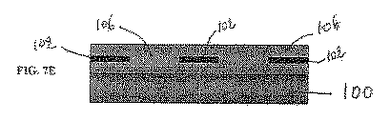
図7A〜7Eは、本発明の他の実施形態による、半絶縁(SI)エピタキシャル層を形成するための各手順を描出する。図7A〜7Dは図4A〜4Dに例示される方法の変法である実施形態を例示する。この実施形態においては、図4A〜4Dに描出された実施形態と同様に、基板上に形成されたエピタキシャル層、すなわち基板に隣接するエピタキシャル層をホウ素源として使用してもよい。しかし、この実施形態においてはマスク材料をホウ素注入領域の表面に適用する。具体的には、図7Aに描出するように、基板100が提供される。基板100は炭化ケイ素を含んでもよい。基板100はあらゆる種類、たとえばn+型SiC基板などとすることができる。図6Aに描出するように、エピタキシャル層101を基板100上に形成する。1つの実施形態においては、エピタキシャル層101はn型エピタキシャル層である。エピタキシャル層101の形成後、図7Bに描出するように、エピタキシャル層101の表面がホウ素イオンで衝撃されてホウ素注入領域102が形成される。エピタキシャル層101の表面上にマスク領域および非マスク領域を区画するよう、エピタキシャル層101のホウ素注入領域102上にマスク材料103を適用する。マスク材料103を適用した後、図7Cに描出するように、たとえばエピタキシャル層101の非マスク(非保護)領域およびホウ素注入領域102の非マスク領域をエッチングすることなどにより、トレンチ104を形成する。
7A-7E depict steps for forming a semi-insulating (SI) epitaxial layer according to another embodiment of the present invention. 7A-7D illustrate an embodiment that is a variation of the method illustrated in FIGS. 4A-4D. In this embodiment, as in the embodiment depicted in FIGS. 4A-4D, an epitaxial layer formed on the substrate, ie, an epitaxial layer adjacent to the substrate, may be used as the boron source. However, in this embodiment, the mask material is applied to the surface of the boron implantation region. Specifically, a
トレンチ104を形成した後、図7Dに描出するようにマスク材料103を除去し、さらにエピタキシャル層101上およびホウ素注入領域102上にもう1つのエピタキシャル層105を成長させる。これはトレンチ104を充填しかつトレンチ104上で自己平坦化するプロセスを用いて実施する。図7Eに描出するように、エピタキシャル層105の成長時、ホウ素領域102内のホウ素がエピタキシャル層101および105に拡散してD−センターを生成し、半絶縁エピタキシャル層106を形成する。
After the
上述の方法は、その全内容を本明細書に参照文献として援用する、「炭化ケイ素内にエピタキシャル成長ドリフト、埋没ゲートおよびガードリング、自己平坦化チャンネルおよびソース領域を有する垂直トレンチ接合電界効果トランジスタ」という標題の、2005年8月8日出願のLin ChengとMichael S.Mazzolaによる米国特許明細書第11/198,298号内にその実施例を確認できる多様なデバイスの二次加工に使用することができる。チャンネルのサイズは、数μm単位であるホウ素の予測拡散長およびホウ素関連D−センターの生成範囲と一致しなければならない。 The above-described method is referred to as a “vertical trench junction field effect transistor having epitaxial growth drift, buried gate and guard ring, self-planarized channel and source region in silicon carbide,” the entire contents of which are incorporated herein by reference. In the title, Lin Cheng and Michael S., filed Aug. 8, 2005. It can be used for the secondary fabrication of a variety of devices whose examples can be found in US patent application Ser. No. 11 / 198,298 by Mazzola. The channel size must be consistent with the expected diffusion length of boron, which is in the order of several μm, and the range of formation of boron-related D-centers.
上述の方法の変法は、D−センター補償の深度も決定し、したがって形成された半絶縁エピタキシャル層106の厚さも決定するホウ素の予想拡散深度よりも厚いわずかにn型のエピタキシャル層101を用いることができる。その結果、基板100と半絶縁エピタキシャル層106の間に残った半導体は残留n型エピタキシャル層101によって占められる。
Variations on the above method use a slightly n-type epitaxial layer 101 that also determines the depth of the D-center compensation, and thus also the expected diffusion depth of boron, which also determines the thickness of the formed semi-insulating epitaxial layer 106. be able to. As a result, the remaining semiconductor between the
1つの実施形態では、基板あるいは隣接するエピタキシャル層内にホウ素を注入するために、基板あるいは隣接するエピタキシャル層を約80keV〜160keVのエネルギーを有するホウ素イオンで衝撃する。1つの実施形態では、合計線量1.23×1015cm−2を有する3つのエネルギー(80keV、115keVおよび160keV)のホウ素注入スキームを適用して、ホウ素に富んだ表面近傍層を形成する。 In one embodiment, the substrate or adjacent epitaxial layer is bombarded with boron ions having an energy of about 80 keV to 160 keV to implant boron into the substrate or adjacent epitaxial layer. In one embodiment, a three energy (80 keV, 115 keV, and 160 keV) boron implantation scheme with a total dose of 1.23 × 10 15 cm −2 is applied to form a boron rich near-surface layer.
本発明の多様な実施形態を、超短波(VHF)からXバンド(10GHz)の上より操作するコンパクトソリッドステートテレビジョンおよびレーダートランスミッターにおける用途に使用することができる。本発明の多様な実施形態は、たとえば最新型軍用機の空中レーダーシステムなどの軍事用途に対しても用いることができる。商業用途には、テレビ放送局、携帯電話基地局、および電話、音声および画像送信のための衛星通信リンクにおける本発明の実施形態の使用が含まれる。さらに、コンパクトな直流−直流(DC−DC)コンバーターを利用した効率のよい電源切り替えおよびモータードライブ制御サーキットリーも、たとえばハイブリッド電気自動車および蛍光照明バラストなどにおいて本発明の実施形態を利用することができる。 Various embodiments of the present invention can be used for applications in compact solid-state televisions and radar transmitters operating from the very high frequency (VHF) to the X band (10 GHz). Various embodiments of the present invention can also be used for military applications such as, for example, aerial radar systems for modern military aircraft. Commercial applications include the use of embodiments of the present invention in television broadcast stations, mobile phone base stations, and satellite communication links for telephone, voice and image transmission. In addition, efficient power supply switching and motor drive control circuitry utilizing a compact DC-DC (DC-DC) converter can also utilize embodiments of the present invention, such as in hybrid electric vehicles and fluorescent lighting ballasts. .
本発明の多様な実施形態が上に記載されているものの、例示の意図で提示されたものであって制限ではないことを理解すべきである。本発明の趣旨および範囲を逸脱することなくその形態および詳細に多様な変更を行えることが、当業者に明らかとなるであろう。実際に、上記の記述を読んだ後で、本発明をどのようにして代替的な実施形態で実行するかが当業者に明らかになるであろう。したがって、本発明は上記の例示的実施形態のいずれによっても制限されるべきではない。 While various embodiments of the present invention have been described above, it should be understood that they have been presented for purposes of illustration and not limitation. It will be apparent to those skilled in the art that various modifications can be made in form and detail without departing from the spirit and scope of the invention. Indeed, after reading the above description, it will become apparent to one skilled in the art how to implement the invention in alternative embodiments. Accordingly, the present invention should not be limited by any of the above-described exemplary embodiments.
さらに、本発明の方法および機器は、半導体技術において使用される関連機器及び方法と同様、本質的に複雑であり、操作パラメータの適切な数値を経験的に決定することにより、あるいはコンピュータシミュレーションを実施して所与の用途にとって最良のデザインに到達することにより最良に実現されることが多い。したがって、全ての適切な変更、組合せおよび同等物は本発明の趣旨および範囲内にあると見なすべきである。 Furthermore, the method and apparatus of the present invention are inherently complex, as are the related equipment and methods used in semiconductor technology, and by performing empirical determinations of appropriate numerical values of operating parameters or performing computer simulations. Thus, it is often best achieved by reaching the best design for a given application. Accordingly, all suitable modifications, combinations and equivalents are to be considered within the spirit and scope of the invention.
さらに、図面は例示の目的のみで提示されることを理解すべきである。本発明の方法およびデバイスは十分に柔軟性および適合性があるので、添付の図面に示す方法以外の方法で使用してもよい。 Further, it should be understood that the drawings are presented for illustrative purposes only. The methods and devices of the present invention are sufficiently flexible and compatible that they may be used in ways other than those shown in the accompanying drawings.
さらに、開示の要約の目的は、一般に米国特許庁および公衆、および特に特許あるいは法律の用語あるいは文体に精通していない科学者、技術者および当技術分野の実践者が、本明細書の技術的開示の性質および本質のおおざっぱな検証から迅速に判断できるようにすることである。開示の要約は、いかなる意味においても本発明の範囲について限定することを意図していない。 Further, the purpose of the disclosure summary is generally that the US Patent Office and the public, and in particular, scientists, engineers, and practitioners in the field who are not familiar with patent or legal terminology or style, To be able to quickly determine from a rough examination of the nature and nature of the disclosure. The summary of the disclosure is not intended to limit the scope of the invention in any way.
Claims (10)
前記基板の前記ホウ素注入領域上あるいは前記第1のエピタキシャル層の前記ホウ素注入領域上に第2のエピタキシャル層を成長させること、および
前記基板あるいは前記第1のエピタキシャル層の前記ホウ素注入領域から前記第2のエピタキシャル層に固相拡散によりホウ素を拡散させることにより、前記第2のエピタキシャル層の少なくとも一部に半絶縁エピタキシャル層を形成することを含む、半絶縁エピタキシャル層を製造する方法。 Implanting boron ions into the substrate or the first epitaxial layer formed on the substrate to form a boron implanted region on the surface of the substrate or the surface of the first epitaxial layer;
Growing a second epitaxial layer on the boron implantation region of the substrate or on the boron implantation region of the first epitaxial layer; and from the boron implantation region of the substrate or the first epitaxial layer. A method for producing a semi-insulating epitaxial layer, comprising: forming a semi-insulating epitaxial layer on at least a part of the second epitaxial layer by diffusing boron into the two epitaxial layers by solid phase diffusion.
(a) 約1500℃と約1700℃の間の温度で前記第2のエピタキシャル層を成長させることを含むか、又は、
(b) 約1時間と約3時間の間の時間で前記第2のエピタキシャル層を成長させることを含むか、又は、
(c)n型の第2のエピタキシャル層を成長させることを含む、
請求項1〜4のいずれか一項に記載の方法。 Growing the second epitaxial layer;
(a) growing the second epitaxial layer at a temperature between about 1500 ° C. and about 1700 ° C., or
(b) growing the second epitaxial layer in a time between about 1 hour and about 3 hours, or
(c) growing an n-type second epitaxial layer;
The method as described in any one of Claims 1-4.
(a)前記第1のエピタキシャル層上および前記ホウ素注入領域上に前記第2のエピタキシャル層を成長させることが前記トレンチを充填することおよび前記トレンチ上で前記第2のエピタキシャル層を平坦化すること含むか、又は、
(b) 前記半絶縁エピタキシャル層を形成するために前記第1のエピタキシャル層上で前記第2のエピタキシャル層が成長する際に前記ホウ素注入領域内のホウ素が前記第1および前記第2のエピタキシャル層内に拡散する、
請求項9に記載の方法。 Further comprising removing the mask material and growing the second epitaxial layer on the first epitaxial layer and on the boron implanted region,
(a) growing the second epitaxial layer on the first epitaxial layer and on the boron implanted region filling the trench and planarizing the second epitaxial layer on the trench Contains or
(b) When the second epitaxial layer is grown on the first epitaxial layer to form the semi-insulating epitaxial layer, boron in the boron implantation region is converted into the first and second epitaxial layers. Diffuse in,
The method of claim 9.
Applications Claiming Priority (5)
| Application Number | Priority Date | Filing Date | Title |
|---|---|---|---|
| US80513906P | 2006-06-19 | 2006-06-19 | |
| US60/805,139 | 2006-06-19 | ||
| US11/764,593 | 2007-06-18 | ||
| US11/764,593 US7821015B2 (en) | 2006-06-19 | 2007-06-18 | Silicon carbide and related wide-bandgap transistors on semi insulating epitaxy |
| PCT/US2007/071549 WO2007149849A1 (en) | 2006-06-19 | 2007-06-19 | Silicon carbide and related wide-bandgap transistors on semi insulating epitaxy |
Publications (3)
| Publication Number | Publication Date |
|---|---|
| JP2009542005A JP2009542005A (en) | 2009-11-26 |
| JP2009542005A5 JP2009542005A5 (en) | 2012-11-29 |
| JP5580045B2 true JP5580045B2 (en) | 2014-08-27 |
Family
ID=38833766
Family Applications (1)
| Application Number | Title | Priority Date | Filing Date |
|---|---|---|---|
| JP2009516677A Expired - Fee Related JP5580045B2 (en) | 2006-06-19 | 2007-06-19 | Silicon carbide and related wide band gap transistors on semi-insulating epitaxy |
Country Status (10)
| Country | Link |
|---|---|
| US (3) | US7821015B2 (en) |
| EP (1) | EP2030243A1 (en) |
| JP (1) | JP5580045B2 (en) |
| KR (1) | KR101418615B1 (en) |
| CN (1) | CN102723360A (en) |
| AU (1) | AU2007261054B2 (en) |
| CA (1) | CA2654634A1 (en) |
| NZ (1) | NZ572662A (en) |
| PH (1) | PH12012501605A1 (en) |
| WO (1) | WO2007149849A1 (en) |
Families Citing this family (21)
| Publication number | Priority date | Publication date | Assignee | Title |
|---|---|---|---|---|
| US7821015B2 (en) | 2006-06-19 | 2010-10-26 | Semisouth Laboratories, Inc. | Silicon carbide and related wide-bandgap transistors on semi insulating epitaxy |
| US8193537B2 (en) | 2006-06-19 | 2012-06-05 | Ss Sc Ip, Llc | Optically controlled silicon carbide and related wide-bandgap transistors and thyristors |
| US8330170B2 (en) * | 2008-12-05 | 2012-12-11 | Micron Technology, Inc. | Semiconductor device structures including transistors with energy barriers adjacent to transistor channels and associated methods |
| EP2443658A4 (en) * | 2009-06-19 | 2013-08-07 | Ss Sc Ip Llc | Methods of making vertical junction field effect transistors and bipolar junction transistors without ion implantation and devices made therewith |
| JP5343904B2 (en) * | 2010-03-23 | 2013-11-13 | 住友電気工業株式会社 | Semiconductor device |
| US8980737B2 (en) * | 2012-05-24 | 2015-03-17 | International Business Machines Corporation | Methods of forming contact regions using sacrificial layers |
| US8889529B2 (en) | 2012-05-24 | 2014-11-18 | International Business Machines Corporation | Heterojunction bipolar transistors with thin epitaxial contacts |
| US9064924B2 (en) | 2012-05-24 | 2015-06-23 | International Business Machines Corporation | Heterojunction bipolar transistors with intrinsic interlayers |
| US9093548B2 (en) | 2012-06-06 | 2015-07-28 | International Business Machines Corporation | Thin film hybrid junction field effect transistor |
| US8665013B2 (en) * | 2012-07-25 | 2014-03-04 | Raytheon Company | Monolithic integrated circuit chip integrating multiple devices |
| US11309389B2 (en) * | 2012-11-30 | 2022-04-19 | Lx Semicon Co., Ltd. | Epitaxial wafer and switch element and light-emitting element using same |
| US9087705B2 (en) | 2013-06-05 | 2015-07-21 | International Business Machines Corporation | Thin-film hybrid complementary circuits |
| SE1430022A1 (en) * | 2013-07-01 | 2015-01-02 | Cheap semi-insulating SiC substrates | |
| EP3036770B1 (en) * | 2013-08-23 | 2022-03-02 | Intel Corporation | High resistance layer for iii-v channel deposited on group iv substrates for mos transistors |
| US10128364B2 (en) | 2016-03-28 | 2018-11-13 | Nxp Usa, Inc. | Semiconductor devices with an enhanced resistivity region and methods of fabrication therefor |
| US10644142B2 (en) | 2017-12-22 | 2020-05-05 | Nxp Usa, Inc. | Semiconductor devices with doped regions functioning as enhanced resistivity regions or diffusion barriers, and methods of fabrication therefor |
| CN108417624B (en) * | 2018-05-11 | 2021-02-02 | 安徽工业大学 | IGBT for improving short circuit robustness and preparation method thereof |
| CN108417638B (en) * | 2018-05-11 | 2021-02-02 | 安徽工业大学 | MOSFET (Metal-oxide-semiconductor field Effect transistor) containing semi-insulating region and preparation method thereof |
| CN108417623B (en) * | 2018-05-11 | 2021-02-02 | 安徽工业大学 | IGBT (insulated Gate Bipolar transistor) containing semi-insulating region and preparation method thereof |
| CN108649064B (en) * | 2018-05-11 | 2021-03-16 | 安徽工业大学 | MOSFET for improving UIS avalanche tolerance and preparation method thereof |
| CN113774494B (en) * | 2021-11-15 | 2022-03-29 | 浙江大学杭州国际科创中心 | Stripping method and stripping device for semi-insulating silicon carbide single crystal wafer |
Family Cites Families (33)
| Publication number | Priority date | Publication date | Assignee | Title |
|---|---|---|---|---|
| JPS5226974B2 (en) * | 1973-02-14 | 1977-07-18 | ||
| US4207583A (en) * | 1978-07-27 | 1980-06-10 | Electric Power Research Institute, Inc. | Multiple gated light fired thyristor with non-critical light pipe coupling |
| JPS5625743A (en) | 1979-08-08 | 1981-03-12 | Matsushita Electric Ind Co Ltd | Electrophotographic receptor |
| US4465750A (en) * | 1981-12-22 | 1984-08-14 | Canon Kabushiki Kaisha | Photoconductive member with a -Si having two layer regions |
| US4825061A (en) * | 1987-08-07 | 1989-04-25 | Center For Innovative Technology | Optically controlled bulk semiconductor switch not requiring radiation to sustain conduction |
| US4947218A (en) * | 1987-11-03 | 1990-08-07 | North Carolina State University | P-N junction diodes in silicon carbide |
| US5135885A (en) * | 1989-03-27 | 1992-08-04 | Sharp Corporation | Method of manufacturing silicon carbide fets |
| US5270554A (en) * | 1991-06-14 | 1993-12-14 | Cree Research, Inc. | High power high frequency metal-semiconductor field-effect transistor formed in silicon carbide |
| US5385855A (en) * | 1994-02-24 | 1995-01-31 | General Electric Company | Fabrication of silicon carbide integrated circuits |
| USH1717H (en) * | 1995-11-16 | 1998-04-07 | The United States Of America As Represented By The Secretary Of The Navy | Bistable photoconductive switches particularly suited for frequency-agile, radio-frequency sources |
| US6680489B1 (en) * | 1995-12-20 | 2004-01-20 | Advanced Technology Materials, Inc. | Amorphous silicon carbide thin film coating |
| US6046466A (en) * | 1997-09-12 | 2000-04-04 | Nikon Corporation | Solid-state imaging device |
| US6063186A (en) * | 1997-12-17 | 2000-05-16 | Cree, Inc. | Growth of very uniform silicon carbide epitaxial layers |
| US6100169A (en) * | 1998-06-08 | 2000-08-08 | Cree, Inc. | Methods of fabricating silicon carbide power devices by controlled annealing |
| JP3430083B2 (en) * | 1999-10-21 | 2003-07-28 | 本田技研工業株式会社 | Battery voltage measuring device |
| WO2002054449A2 (en) * | 2001-01-03 | 2002-07-11 | Mississippi State University | Silicon carbide and related wide-bandgap transistors on semi-insulating epitaxy for high-speed, high-power applications |
| WO2003075319A2 (en) * | 2001-07-12 | 2003-09-12 | Mississippi State University | Self-aligned transistor and diode topologies |
| US7498066B2 (en) | 2002-05-08 | 2009-03-03 | Btu International Inc. | Plasma-assisted enhanced coating |
| US20060228497A1 (en) | 2002-05-08 | 2006-10-12 | Satyendra Kumar | Plasma-assisted coating |
| US20050233091A1 (en) | 2002-05-08 | 2005-10-20 | Devendra Kumar | Plasma-assisted coating |
| JP2004247545A (en) * | 2003-02-14 | 2004-09-02 | Nissan Motor Co Ltd | Semiconductor device and its fabrication process |
| KR100593264B1 (en) | 2003-06-26 | 2006-06-26 | 학교법인 포항공과대학교 | P-n heterojunction structure of zinc oxide nanorod with semiconductive substrate, preparation thereof, and device using same |
| TWI228320B (en) * | 2003-09-09 | 2005-02-21 | Ind Tech Res Inst | An avalanche photo-detector(APD) with high saturation power, high gain-bandwidth product |
| US7470967B2 (en) * | 2004-03-12 | 2008-12-30 | Semisouth Laboratories, Inc. | Self-aligned silicon carbide semiconductor devices and methods of making the same |
| JP4832723B2 (en) * | 2004-03-29 | 2011-12-07 | 日本碍子株式会社 | Semiconductor device having active high resistance semiconductor layer |
| US20060062897A1 (en) | 2004-09-17 | 2006-03-23 | Applied Materials, Inc | Patterned wafer thickness detection system |
| US7569900B2 (en) * | 2004-11-16 | 2009-08-04 | Kabushiki Kaisha Toshiba | Silicon carbide high breakdown voltage semiconductor device |
| US7642205B2 (en) | 2005-04-08 | 2010-01-05 | Mattson Technology, Inc. | Rapid thermal processing using energy transfer layers |
| US20070029573A1 (en) * | 2005-08-08 | 2007-02-08 | Lin Cheng | Vertical-channel junction field-effect transistors having buried gates and methods of making |
| JP2006080560A (en) | 2005-10-31 | 2006-03-23 | Kansai Electric Power Co Inc:The | Optical coupling power semiconductor device |
| US7582917B2 (en) | 2006-03-10 | 2009-09-01 | Bae Systems Information And Electronic Systems Integration Inc. | Monolithically integrated light-activated thyristor and method |
| US7274083B1 (en) | 2006-05-02 | 2007-09-25 | Semisouth Laboratories, Inc. | Semiconductor device with surge current protection and method of making the same |
| US7821015B2 (en) | 2006-06-19 | 2010-10-26 | Semisouth Laboratories, Inc. | Silicon carbide and related wide-bandgap transistors on semi insulating epitaxy |
-
2007
- 2007-06-18 US US11/764,593 patent/US7821015B2/en not_active Expired - Fee Related
- 2007-06-19 EP EP07784481A patent/EP2030243A1/en not_active Withdrawn
- 2007-06-19 WO PCT/US2007/071549 patent/WO2007149849A1/en active Application Filing
- 2007-06-19 CN CN2012101529494A patent/CN102723360A/en active Pending
- 2007-06-19 NZ NZ572662A patent/NZ572662A/en not_active IP Right Cessation
- 2007-06-19 JP JP2009516677A patent/JP5580045B2/en not_active Expired - Fee Related
- 2007-06-19 KR KR1020097000874A patent/KR101418615B1/en active IP Right Grant
- 2007-06-19 AU AU2007261054A patent/AU2007261054B2/en not_active Ceased
- 2007-06-19 CA CA002654634A patent/CA2654634A1/en not_active Abandoned
-
2010
- 2010-09-14 US US12/881,771 patent/US8183124B2/en active Active - Reinstated
-
2012
- 2012-04-18 US US13/449,502 patent/US8592826B2/en active Active
- 2012-08-09 PH PH12012501605A patent/PH12012501605A1/en unknown
Also Published As
| Publication number | Publication date |
|---|---|
| KR101418615B1 (en) | 2014-07-14 |
| CN102723360A (en) | 2012-10-10 |
| US8183124B2 (en) | 2012-05-22 |
| AU2007261054B2 (en) | 2013-09-26 |
| CA2654634A1 (en) | 2007-12-27 |
| US20110003456A1 (en) | 2011-01-06 |
| JP2009542005A (en) | 2009-11-26 |
| PH12012501605A1 (en) | 2015-01-26 |
| AU2007261054A1 (en) | 2007-12-27 |
| US20120199940A1 (en) | 2012-08-09 |
| KR20090033224A (en) | 2009-04-01 |
| US8592826B2 (en) | 2013-11-26 |
| US20070290212A1 (en) | 2007-12-20 |
| NZ572662A (en) | 2012-02-24 |
| WO2007149849A1 (en) | 2007-12-27 |
| US7821015B2 (en) | 2010-10-26 |
| EP2030243A1 (en) | 2009-03-04 |
Similar Documents
| Publication | Publication Date | Title |
|---|---|---|
| JP5580045B2 (en) | Silicon carbide and related wide band gap transistors on semi-insulating epitaxy | |
| US7432171B2 (en) | Silicon carbide and related wide-bandgap transistors on semi-insulating epitaxy for high-speed, high-power applications | |
| US7183175B2 (en) | Shallow trench isolation structure for strained Si on SiGe | |
| JP2004014856A (en) | Method for manufacturing semiconductor substrate and semiconductor device | |
| JP2009542005A5 (en) | ||
| KR100858154B1 (en) | A wafer and a process for forming wafer | |
| US20050217566A1 (en) | Method for producing one or more monocrystalline layers, each with a different lattice structure, on one plane of a series of layers | |
| JP2002203965A (en) | Semiconductor device | |
| JP6125568B2 (en) | Optimization layer for semiconductors | |
| CN101473442B (en) | Silicon carbide and related wide-bandgap transistors on semi insulating epitaxy | |
| JP7163575B2 (en) | Silicon carbide semiconductor substrate and method for manufacturing silicon carbide semiconductor substrate | |
| JP2009147246A (en) | Silicon carbide semiconductor substrate, method of manufacturing silicon carbide semiconductor substrate, silicon carbide semiconductor bulk crystal, method of manufacturing silicon carbide semiconductor bulk crystal, silicon carbide semiconductor device and method of manufacturing silicon carbide semiconductor device | |
| US8658500B2 (en) | Single crystal U-MOS gates using microwave crystal regrowth | |
| CN1624921A (en) | CMOS on hybrid substrate with different crystal orientations using silicon-to-silicon direct wafer bonding | |
| JPWO2020012605A1 (en) | Semiconductor devices and methods for manufacturing semiconductor devices | |
| JP2007123469A (en) | Semiconductor device and its manufacturing method | |
| US10431454B2 (en) | Semiconductor substrate and manufacturing method thereof | |
| CN104716045A (en) | Manufacturing method for improving interface state after SiC thermal oxidation | |
| Regolini et al. | Epitaxial growth of SiGe layers for BiCMOS applications | |
| JP2021019164A (en) | Method for manufacturing epitaxial silicon wafer, epitaxial silicon wafer, method for manufacturing silicon wafer, silicon wafer, and method for manufacturing semiconductor device | |
| JP2001189320A (en) | Semiconductor device and manufacturing method therefor | |
| JPH06120241A (en) | Manufacture of semiconductor device | |
| JPH0428235A (en) | Manufacture of semiconductor device |
Legal Events
| Date | Code | Title | Description |
|---|---|---|---|
| A521 | Written amendment |
Free format text: JAPANESE INTERMEDIATE CODE: A523 Effective date: 20100618 |
|
| A621 | Written request for application examination |
Free format text: JAPANESE INTERMEDIATE CODE: A621 Effective date: 20100618 |
|
| A711 | Notification of change in applicant |
Free format text: JAPANESE INTERMEDIATE CODE: A711 Effective date: 20111102 |
|
| A521 | Written amendment |
Free format text: JAPANESE INTERMEDIATE CODE: A523 Effective date: 20121008 |
|
| A977 | Report on retrieval |
Free format text: JAPANESE INTERMEDIATE CODE: A971007 Effective date: 20121018 |
|
| A131 | Notification of reasons for refusal |
Free format text: JAPANESE INTERMEDIATE CODE: A131 Effective date: 20121113 |
|
| A601 | Written request for extension of time |
Free format text: JAPANESE INTERMEDIATE CODE: A601 Effective date: 20130212 |
|
| A602 | Written permission of extension of time |
Free format text: JAPANESE INTERMEDIATE CODE: A602 Effective date: 20130219 |
|
| A601 | Written request for extension of time |
Free format text: JAPANESE INTERMEDIATE CODE: A601 Effective date: 20130311 |
|
| A521 | Written amendment |
Free format text: JAPANESE INTERMEDIATE CODE: A523 Effective date: 20130318 |
|
| A602 | Written permission of extension of time |
Free format text: JAPANESE INTERMEDIATE CODE: A602 Effective date: 20130318 |
|
| A131 | Notification of reasons for refusal |
Free format text: JAPANESE INTERMEDIATE CODE: A131 Effective date: 20130709 |
|
| A601 | Written request for extension of time |
Free format text: JAPANESE INTERMEDIATE CODE: A601 Effective date: 20131008 |
|
| A602 | Written permission of extension of time |
Free format text: JAPANESE INTERMEDIATE CODE: A602 Effective date: 20131016 |
|
| A131 | Notification of reasons for refusal |
Free format text: JAPANESE INTERMEDIATE CODE: A131 Effective date: 20140304 |
|
| A521 | Written amendment |
Free format text: JAPANESE INTERMEDIATE CODE: A523 Effective date: 20140505 |
|
| TRDD | Decision of grant or rejection written | ||
| A01 | Written decision to grant a patent or to grant a registration (utility model) |
Free format text: JAPANESE INTERMEDIATE CODE: A01 Effective date: 20140617 |
|
| A61 | First payment of annual fees (during grant procedure) |
Free format text: JAPANESE INTERMEDIATE CODE: A61 Effective date: 20140710 |
|
| R150 | Certificate of patent or registration of utility model |
Ref document number: 5580045 Country of ref document: JP Free format text: JAPANESE INTERMEDIATE CODE: R150 |
|
| LAPS | Cancellation because of no payment of annual fees |