JP5577859B2 - Manufacturing method of electronic device - Google Patents
Manufacturing method of electronic device Download PDFInfo
- Publication number
- JP5577859B2 JP5577859B2 JP2010128771A JP2010128771A JP5577859B2 JP 5577859 B2 JP5577859 B2 JP 5577859B2 JP 2010128771 A JP2010128771 A JP 2010128771A JP 2010128771 A JP2010128771 A JP 2010128771A JP 5577859 B2 JP5577859 B2 JP 5577859B2
- Authority
- JP
- Japan
- Prior art keywords
- substrate
- resin sheet
- electronic components
- resin
- connection
- Prior art date
- Legal status (The legal status is an assumption and is not a legal conclusion. Google has not performed a legal analysis and makes no representation as to the accuracy of the status listed.)
- Expired - Fee Related
Links
Images


Classifications
-
- H—ELECTRICITY
- H01—ELECTRIC ELEMENTS
- H01L—SEMICONDUCTOR DEVICES NOT COVERED BY CLASS H10
- H01L24/00—Arrangements for connecting or disconnecting semiconductor or solid-state bodies; Methods or apparatus related thereto
- H01L24/93—Batch processes
- H01L24/95—Batch processes at chip-level, i.e. with connecting carried out on a plurality of singulated devices, i.e. on diced chips
-
- H—ELECTRICITY
- H01—ELECTRIC ELEMENTS
- H01L—SEMICONDUCTOR DEVICES NOT COVERED BY CLASS H10
- H01L2924/00—Indexing scheme for arrangements or methods for connecting or disconnecting semiconductor or solid-state bodies as covered by H01L24/00
- H01L2924/10—Details of semiconductor or other solid state devices to be connected
- H01L2924/11—Device type
- H01L2924/13—Discrete devices, e.g. 3 terminal devices
- H01L2924/1304—Transistor
- H01L2924/1306—Field-effect transistor [FET]
- H01L2924/13091—Metal-Oxide-Semiconductor Field-Effect Transistor [MOSFET]
-
- H—ELECTRICITY
- H01—ELECTRIC ELEMENTS
- H01L—SEMICONDUCTOR DEVICES NOT COVERED BY CLASS H10
- H01L2924/00—Indexing scheme for arrangements or methods for connecting or disconnecting semiconductor or solid-state bodies as covered by H01L24/00
- H01L2924/15—Details of package parts other than the semiconductor or other solid state devices to be connected
- H01L2924/151—Die mounting substrate
- H01L2924/156—Material
- H01L2924/15786—Material with a principal constituent of the material being a non metallic, non metalloid inorganic material
- H01L2924/15787—Ceramics, e.g. crystalline carbides, nitrides or oxides
Description
本発明は、基板の一面上に電子部品を搭載するとともに、電子部品を封止樹脂で封止してなる電子装置の製造方法に関する。 The present invention relates to a method for manufacturing an electronic device in which an electronic component is mounted on one surface of a substrate and the electronic component is sealed with a sealing resin.
一般に、この種の電子装置は、一面上に基板電極を有する基板を用い、この基板の一面上に、電子部品を搭載して、電子部品と基板電極とを導電性接着剤やはんだなどにより電気的に接続し、その後、トランスファーモールド法などにより、基板の一面上にて電子部品、および、電子部品と基板電極との接続部を、封止樹脂で封止することにより、製造される。 In general, this type of electronic device uses a substrate having a substrate electrode on one surface, the electronic component is mounted on one surface of the substrate, and the electronic component and the substrate electrode are electrically connected by a conductive adhesive or solder. After that, the electronic component and the connection part between the electronic component and the substrate electrode are sealed with a sealing resin on one surface of the substrate by a transfer molding method or the like.
ここにおいて、電子部品は複数個存在するため、これら複数個の電子部品を一括して基板の一面上に実装することによって、タクトタイムを短縮したいという要望がある。 Here, since there are a plurality of electronic components, there is a desire to shorten the tact time by mounting the plurality of electronic components together on one surface of the substrate.
これに対して、特許文献1には、電子部品に応じた彫りこみを有する治具を用い、この治具の彫り込みに電子部品をその実装面を上にして搭載し、その上に、はんだペーストを印刷した基板を治具に合わせて載せた後、一括してリフローにかける方法が提案されている。 On the other hand, in Patent Document 1, a jig having an engraving corresponding to an electronic component is used, and the electronic component is mounted with the mounting surface facing upward in engraving the jig, and a solder paste is placed thereon. There has been proposed a method in which a printed substrate is put together with a jig and then reflowed together.
これにより、複数の電子部品を一括して基板に搭載することができるが、その後、さらに封止樹脂によって、電子部品および電子部品と基板電極との接続部の封止を行うため、部品搭載後に、別途、これら樹脂による封止工程が必要となる。 As a result, a plurality of electronic components can be mounted on the substrate in a lump. After that, the sealing portion further seals the electronic component and the connection portion between the electronic component and the substrate electrode. Separately, a sealing step with these resins is required.
一方、特許文献2では、複数の電子部品を一括して基板に搭載する方法として、あらかじめ複数の発熱素子をヒートシンク上に接着剤で貼り付けておくことにより、基板上に複数の発熱素子を一括してはんだ付けする方法が提案されている。これにより、電子部品の一括接続を達成することができるが、電子部品の高さが異なる場合には、対応することができない。
On the other hand, in
また、特許文献3、4には、複数の電子部品を仮基板に置き、その状態で樹脂による封止を行い、樹脂の硬化を完了させた後、樹脂ごと仮基板からはずすことで複数の電子部品を一個のワークとして扱うことにより、正規の基板への複数の電子部品の一括接続を可能とする方法が提案されている。
In
しかし、この場合、電子部品は封止樹脂で封止されているものの、封止樹脂から露出する電子部品の接続面と基板上の基板電極との電気的な接続部に対して、さらに、別の樹脂などを用いて封止する必要があり、そのためのコストや手間が必要となる。 However, in this case, although the electronic component is sealed with the sealing resin, it is further separated from the electrical connection portion between the connection surface of the electronic component exposed from the sealing resin and the substrate electrode on the substrate. It is necessary to seal using a resin or the like, which requires cost and labor.
いずれにせよ、従来では、基板の一面上に電子部品を搭載して電子部品と基板電極とを電気的に接続し、さらに、基板の一面上にて電子部品および電子部品と基板電極との接続部を封止樹脂で封止してなる電子装置を製造するにあたって、電子部品の搭載と封止樹脂による封止とを一括して行える方法はなかった。なお、このことは、電子部品が複数であれ単数であれ、共通の問題である。 In any case, conventionally, an electronic component is mounted on one surface of the substrate to electrically connect the electronic component and the substrate electrode, and further, the electronic component and the electronic component are connected to the substrate electrode on one surface of the substrate. In manufacturing an electronic device in which a portion is sealed with a sealing resin, there has been no method capable of collectively mounting electronic components and sealing with a sealing resin. This is a common problem regardless of whether the electronic component is plural or singular.
本発明は、上記問題に鑑みてなされたものであり、基板の一面上に電子部品を搭載するとともに、電子部品を封止樹脂で封止してなる電子装置を製造するにあたって、電子部品の搭載と、封止樹脂による電子部品および電子部品と基板電極との接続部封止とを一括して行えるようにすることを目的とする。 The present invention has been made in view of the above problems, and in mounting an electronic component on one surface of a substrate and manufacturing an electronic device in which the electronic component is sealed with a sealing resin, the mounting of the electronic component is performed. It is another object of the present invention to collectively perform sealing of an electronic component using a sealing resin and a connection portion between the electronic component and a substrate electrode.
上記目的を達成するため、請求項1に記載の発明では、一面(11)上に基板電極(20)を有する基板(10)の当該一面(11)上に、電子部品(30)を搭載して電子部品(30〜34)と基板電極(20)とを電気的に接続するとともに、基板(10)の一面(11)上にて電子部品(30〜34)を封止樹脂(40)で封止してなる電子装置の製造方法において、次のような点を有することを特徴としている。 In order to achieve the above object, according to the first aspect of the present invention, the electronic component (30) is mounted on the one surface (11) of the substrate (10) having the substrate electrode (20) on the one surface (11). The electronic component (30-34) and the substrate electrode (20) are electrically connected to each other, and the electronic component (30-34) is sealed with a sealing resin (40) on one surface (11) of the substrate (10). The manufacturing method of the electronic device formed by sealing has the following points.
・Bステージ状態の熱硬化性樹脂よりなる板状の樹脂シート(110)の内部に電子部品(30〜34)を埋め込むとともに、電子部品(30〜34)における基板電極(20)との接続面を樹脂シート(110)の一方の板面(111)にて露出させてなるシート部材(100)と、基板(10)とを用意すること。 The electronic component (30 to 34) is embedded in the plate-shaped resin sheet (110) made of the thermosetting resin in the B stage state, and the connection surface with the substrate electrode (20) in the electronic component (30 to 34) A sheet member (100) that is exposed on one plate surface (111) of the resin sheet (110) and a substrate (10).
・シート部材(100)における樹脂シート(110)の一方の板面(111)と基板(10)の一面(11)とを対向させて、樹脂シート(110)の一方の板面(111)にて露出する電子部品(30〜34)の接続面と、これに接続される基板電極(20)とを位置合わせする位置合わせ工程を行うこと。 -One plate surface (111) of the resin sheet (110) in the sheet member (100) and one surface (11) of the substrate (10) are opposed to one plate surface (111) of the resin sheet (110). And performing an alignment step of aligning the connection surfaces of the electronic components (30 to 34) exposed to the substrate electrodes (20) connected thereto.
・続いて、シート部材(100)を基板(10)側へ押し付けることにより、電子部品(30〜34)の接続面と基板電極(20)とを電気的に接続するとともに、基板電極(20)間にて、樹脂シート(110)が、基板(10)の一面(11)側へ押し込まれるように変形し、基板(10)の一面(11)のうちの基板電極(20)の間の部位に貼り付き、電子部品(30〜34)の直下部分のうち基板電極(20)以外の部位に、変形した樹脂シート(110)が回り込むようにすることで、当該接続面と基板電極(20)との接続部を樹脂シート(110)で封止する封止工程を行うこと。 Subsequently, the sheet member (100) is pressed against the substrate (10) side to electrically connect the connection surfaces of the electronic components (30 to 34) and the substrate electrode (20), and the substrate electrode (20). In the meantime, the resin sheet (110) is deformed so as to be pushed into the one surface (11) side of the substrate (10), and the portion between the substrate electrodes (20) in the one surface (11) of the substrate (10). -out paste to, a part other than the substrate electrode (20) of the portion immediately below the electronic part (30 to 34), the resin sheet (110) which has been deformed by so goes around, the connection surface and the substrate electrode (20 A sealing step of sealing the connecting portion with the resin sheet (110).
・その後、樹脂シート(110)をその硬化温度以上に加熱して完全に硬化させ、この硬化した樹脂シート(110)を封止樹脂(40)とする硬化工程を行うこと。本製造方法は、これらの点を備えることを特徴としている。 -Then, the resin sheet (110) is heated more than the curing temperature to be completely cured, and a curing process is performed in which the cured resin sheet (110) is used as the sealing resin (40). The manufacturing method is characterized by including these points.
本発明は、封止樹脂が熱硬化性樹脂よりなることに着目してなされたもので、それによれば、電子部品(30〜34)を、半硬化状態であるBステージの熱硬化性樹脂よりなる樹脂シート(110)に埋め込んで一体化したシート部材(100)を用い、これを基板(10)の一面(11)上に搭載して、樹脂シート(110)より露出する電子部品(30〜34)の接続面と基板電極(20)とを接続することで、電子部品(30〜34)を封止状態にて搭載することが実現される。 The present invention has been made by paying attention to the fact that the sealing resin is made of a thermosetting resin. According to this, the electronic components (30 to 34) are made from the thermosetting resin of the B stage which is in a semi-cured state. An electronic component (30˜) exposed from the resin sheet (110) is mounted on one surface (11) of the substrate (10) using a sheet member (100) embedded and integrated in the resin sheet (110). By connecting the connection surface 34) and the substrate electrode (20), it is possible to mount the electronic components (30 to 34) in a sealed state.
それとともに、この電子部品(30〜34)の搭載のときに、Bステージの樹脂シート(110)を基板(10)に押し付けて変形させて、基板(10)の一面(11)のうちの基板電極(20)の間の部位に貼り付けることで、当該接続面と基板電極(20)との接続部が樹脂シート(110)で封止されるから、当該接続部の封止が実現される。 At the same time, when the electronic components (30 to 34) are mounted, the resin sheet (110) of the B stage is pressed against the substrate (10) to be deformed, and the substrate of the one surface (11) of the substrate (10). Since the connection portion between the connection surface and the substrate electrode (20) is sealed with the resin sheet (110) by being attached to the portion between the electrodes (20), the connection portion is sealed. .
よって、本発明によれば、電子部品(30〜34)の搭載と、封止樹脂(40)による電子部品(30〜34)および電子部品(30〜34)と基板電極(20)との接続部の封止とを一括して行える。なお、この本発明の効果は、電子部品が単数でも複数でも同様に発揮されることは明らかである。 Therefore, according to the present invention, the mounting of the electronic components (30 to 34) and the connection between the electronic components (30 to 34) and the electronic components (30 to 34) and the substrate electrode (20) by the sealing resin (40). The parts can be sealed together. It is obvious that the effect of the present invention can be similarly achieved regardless of whether the number of electronic components is one or more.
ここで、請求項2に記載の発明では、請求項1に記載の電子装置の製造方法において、電子部品(30〜34)の接続面および当該接続面に接続される基板電極(20)のいずれか一方に、当該一方からこれに接続される相手側に向かって突出する導電性のバンプ(60)を設け、このバンプ(60)を介して当該接続面と基板電極(20)との電気的接続を行い、電子部品(30〜34)の接続面と基板電極(20)との接続部は、当該接続面、バンプ(60)および基板電極(20)により構成されたものとすることを特徴としている。
Here, in the invention according to
樹脂シート(110)の一方の板面(111)からバンプ(60)が突出する形となり、電子部品(30〜34)の接続面と当該一方の板面(111)とが同一平面にある場合に比べれば、基板電極(20)への接続が容易となる。 The bump (60) protrudes from one plate surface (111) of the resin sheet (110), and the connection surface of the electronic component (30 to 34) and the one plate surface (111) are in the same plane. As compared with the above, connection to the substrate electrode (20) is facilitated.
また、請求項3に記載の発明では、請求項1または請求項2に記載の電子装置の製造方法において、用意される前記シート部材(100)においては、電子部品(30〜34)の接続面が樹脂シート(110)の一方の板面(111)より突出させた状態としておき、電子部品(30〜34)の接続面と基板電極(20)との接続部は、樹脂シート(110)の一方の板面(111)より突出する接続面および基板電極(20)により構成されたものとすることを特徴としている。 According to a third aspect of the present invention, in the electronic device manufacturing method according to the first or second aspect, in the prepared sheet member (100), the connection surface of the electronic component (30 to 34). Is protruded from one plate surface (111) of the resin sheet (110), and a connection portion between the connection surface of the electronic component (30 to 34) and the substrate electrode (20) is formed on the resin sheet (110). It is characterized by comprising a connection surface protruding from one plate surface (111) and a substrate electrode (20).
この場合、樹脂シート(110)の一方の板面(111)から電子部品(30〜34)の接続面が突出する形となり、当該接続面と当該一方の板面(111)とが同一平面にある場合に比べれば、基板電極(20)への接続が容易となる。 In this case, the connection surface of the electronic components (30 to 34) protrudes from one plate surface (111) of the resin sheet (110), and the connection surface and the one plate surface (111) are in the same plane. Compared to a certain case, the connection to the substrate electrode (20) becomes easier.
また、請求項1に記載の発明では、用意されるシート部材(100)においては、樹脂シート(110)の他方の板面(112)に金属シート(80)を貼り付けておくことを特徴としている。 Further, characterized in that according the invention described in claim 1, in the sheet member to be use meaning (100), to be affixed to the metal sheet (80) on the other plate surface of the resin sheet (110) (112) It is said.
それによれば、樹脂シート(110)の他方の板面(112)の粘着部分が金属シート(80)で被覆されるので、取り扱い性に優れる。 According to that, since the adhesion part of the other board surface (112) of the resin sheet (110) is coat | covered with the metal sheet (80), it is excellent in handleability.
また、請求項4に記載の発明では、請求項1ないし請求項3のいずれか1つに記載の電子装置の製造方法において、樹脂シート(110)の内部に電子部品(30〜34)を埋め込む工程では、Bステージ状態の熱硬化性樹脂よりなる樹脂シート(110)に、電子部品(30〜34)に対応した形状の凹み(113)を設け、この凹み(113)に電子部品(30〜34)を入れて樹脂シート(110)のタック力により電子部品(30〜34)を樹脂シート(110)に固定することを特徴としている。 According to a fourth aspect of the present invention, in the electronic device manufacturing method according to any one of the first to third aspects, the electronic components (30 to 34) are embedded in the resin sheet (110). In the process, a recess (113) having a shape corresponding to the electronic component (30 to 34) is provided in the resin sheet (110) made of a thermosetting resin in a B stage state, and the electronic component (30 to 34) is provided in the recess (113). 34) and the electronic components (30 to 34) are fixed to the resin sheet (110) by the tack force of the resin sheet (110).
このように樹脂シート(110)がBステージであるから、そのタック力により電子部品(30〜34)を固定することが可能となり、電子部品(30〜34)と樹脂シート(110)の一体化が容易に行える。 Thus, since the resin sheet (110) is a B stage, the electronic component (30 to 34) can be fixed by the tack force, and the electronic component (30 to 34) and the resin sheet (110) are integrated. Can be done easily.
また、請求項5に記載の発明では、請求項1ないし請求項3のいずれか1つに記載の電子装置の製造方法において、樹脂シート(110)の内部に電子部品(30〜34)を埋め込む工程では、Bステージ状態の熱硬化性樹脂よりなる樹脂シート(110)を、電子部品(30〜34)における接続面とは反対側から電子部品(30〜34)に押し付けて、樹脂シート(110)に電子部品(30〜34)をめり込ませることを特徴としている。 According to a fifth aspect of the present invention, in the electronic device manufacturing method according to any one of the first to third aspects, the electronic components (30 to 34) are embedded in the resin sheet (110). In the process, a resin sheet (110) made of a thermosetting resin in a B-stage state is pressed against the electronic component (30-34) from the side opposite to the connection surface of the electronic component (30-34), and the resin sheet (110 ) Is embedded with electronic components (30 to 34).
このように、樹脂シート(110)が加重により変形するBステージであることを利用して、電子部品(30〜34)をめり込ませることで、電子部品(30〜34)と樹脂シート(110)の一体化が容易に行える。 Thus, the electronic component (30-34) and the resin sheet (the resin sheet (110)) are inserted into the electronic component (30-34) by using the B stage that is deformed by weight. 110) can be easily integrated.
なお、特許請求の範囲およびこの欄で記載した各手段の括弧内の符号は、後述する実施形態に記載の具体的手段との対応関係を示す一例である。 In addition, the code | symbol in the bracket | parenthesis of each means described in the claim and this column is an example which shows a corresponding relationship with the specific means as described in embodiment mentioned later.
以下、本発明の実施形態について図に基づいて説明する。なお、以下の各実施形態相互において、互いに同一もしくは均等である部分には、説明の簡略化を図るべく、図中、同一符号を付してある。 Hereinafter, embodiments of the present invention will be described with reference to the drawings. In the following embodiments, parts that are the same or equivalent to each other are given the same reference numerals in the drawings in order to simplify the description.
(第1実施形態)
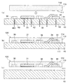
図1は、本発明の第1実施形態に係る電子装置の概略構成を示す図であり、図1において(a)は概略断面図、(b)は概略平面図である。なお、図1(b)は図1(a)の上面図であり、封止樹脂40を透過して、その内部の構成要素を示している。
(First embodiment)
FIG. 1 is a diagram illustrating a schematic configuration of an electronic device according to a first embodiment of the present invention, in which (a) is a schematic cross-sectional view and (b) is a schematic plan view. Note that FIG. 1B is a top view of FIG. 1A and shows the components inside through the sealing
本実施形態の電子装置は、大きくは、一面11上に基板電極20を有する基板10の当該一面11上に、電子部品30〜34を搭載して電子部品30〜34と基板電極20とを電気的に接続するとともに、基板10の一面11上にて電子部品30〜34を封止樹脂40で封止してなる。
The electronic device according to the present embodiment is broadly configured to mount the
基板10は、板状をなすもので、その一方の板面を一面11とし、他方の板面を他面12とする。この基板10としては、プリント基板、セラミック基板などの配線基板が挙げられる。
The
ここでは、基板10は、一面11に表面電極としての基板電極20、他面12に裏面電極21を有する。これら両電極20、21は、たとえばAlやCuなどよりなる一般的なものであり、電子部品30〜34の接続面に対応した形状に、印刷やエッチングなどによりパターニングされている。
Here, the
そして、基板10において、これら両面11、12の電極20、21同士は、基板10の内部に設けられているビアや層間配線としての内部配線22により電気的に接続されている。
In the
そして、ここでは一面11の基板電極20に電子部品30〜34が電気的に接続され、他面12の裏面電極21にて外部との電気的接続が行われるようになっている。これにより、電子部品30〜34は、基板電極20、内部配線22、裏面電極21を介して外部と導通状態とされるようになっている。
Here, the
電子部品30〜34は、基板10の一面11に搭載可能なものならば、特に限定されるものではない。ここでは、複数個の電子部品30〜34が基板10の一面11に搭載されている。電子部品30〜34が複数個の場合、これら複数個のものは同一種類でもよいし、異種のものでもよい。
The
図1の例では、電子部品30〜34としては、チップ抵抗30、突出電極を有するフリップチップ32、チップコンデンサ32、MOSトランジスタなどのパワー素子33、および、このパワー素子33に電気的に接続されたリード部材34が示されている。
In the example of FIG. 1, the
そして、これら電子部品30〜34の接続面、具体的には、チップ抵抗30の電極、フリップチップ31のAuなどよりなる突出電極、チップコンデンサ32の電極、パワー素子33の裏面電極、リード部材34の一端部は、これに対向する基板電極20に対して、一般的なはんだや導電性接着剤などの導電性接合部材50を介して、電気的に接続されている。
The connection surfaces of these
また、封止樹脂40は、電子装置のモールド材料として用いられるエポキシ樹脂などの熱硬化性樹脂よりなる。この封止樹脂40は、基板10の一面11にて、電子部品30〜34、電子部品30〜34と基板電極20との電気的接続部、および、基板10の一面11のうち基板電極20間の部位を封止し、これら被封止部位を保護している。
The sealing
なお、ここでは、電子部品30〜34と基板電極20との電気的接続部は、互いに接続されている電子部品30〜34の接続面と導電性接合部材50と基板電極20とにより構成されるものである。
Here, the electrical connection portion between the
ここで、封止樹脂40について、さらに述べると、封止樹脂40は熱硬化性樹脂であり、半硬化状態(硬化中間状態)であるBステージから完全硬化状態(硬化終了状態)であるCステージまで、硬化されたものである。たとえば、一般的なエポキシ樹脂の場合、たとえば120℃、30分の加熱でBステージ状態とされ、150℃、30分の加熱でCステージ状態とされる。
Here, the sealing
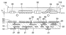
次に、本実施形態の電子装置の製造方法について、図2〜図4を参照して述べる。本製造方法では、予め、電子部品30〜34と封止樹脂40の素材である樹脂とが一体化されたシート部材100を形成し、これを基板10の一面11に取り付けることにより電子装置を製造する。
Next, a method for manufacturing the electronic device of this embodiment will be described with reference to FIGS. In the present manufacturing method, the electronic device is manufactured by previously forming the
ここで、シート部材100の形成は、Bステージ状態の熱硬化性樹脂よりなる板状の樹脂シート110の内部に電子部品30〜34を埋め込むとともに、電子部品30〜34における基板電極20との接続面を樹脂シート110の一方の板面111にて露出させることにより行われる。
Here, the
このシート部材100の具体的な形成方法として、図2に示される第1の形成方法と、図3に示される第2の形成方法とを示す。図2は、シート部材の第1の形成方法を示す工程図であり、各ワークを断面的に示している。図3は、シート部材の第2の形成方法を示す工程図であり、各ワークを断面的に示している。
As a specific method for forming the
まず、第1の形成方法では、金型などにより、Bステージ状態の熱硬化性樹脂よりなる板状の樹脂シート110を形成する。具体的には、金型に投入した熱硬化性樹脂を完全硬化温度未満の温度に加熱してBステージ状態とする。エポキシ樹脂の場合、上述のように、たとえば120℃、30分の加熱を行う。これにより、表裏の関係にある両板面111、112を有する板状の樹脂シート110が形成される。
First, in the first forming method, a plate-shaped
なお、Bステージ状態とは、上記したように、熱硬化性樹脂の硬化中間状態をいうものであり、このBステージについては、たとえば特許第4407456号公報、特許第4390056号公報、特許第4096394号公報等にも記載されている。そして、このBステージの状態での樹脂は、粘着力(タック力)を有するとともに、加重や加熱により軟化する。 As described above, the B stage state refers to an intermediate curing state of the thermosetting resin. For example, Japanese Patent No. 4407456, Japanese Patent No. 4390056, and Japanese Patent No. 4096394 are used for this B stage. It is also described in publications. The resin in the state of the B stage has an adhesive force (tack force) and is softened by weighting or heating.
そして、第1の形成方法では、図2(a)に示されるように、樹脂シート110の一面111に、プレス加工により電子部品30〜34の形状に応じた形に凹んだ凹み113を形成する。その後、図2(b)に示されるように、その凹み113に対して、電子部品30〜34をその接続面を樹脂シート110の一面111に露出させつつ、埋め込む。
And in the 1st formation method, as shown in Drawing 2 (a),
こうして、樹脂シート110の内部に電子部品30〜34を埋め込むことができ、凹み113に入った電子部品30〜34は、Bステージにある樹脂シート110のタック力により樹脂シート110に固定される。なお、このとき樹脂シート110を加熱してタック力を大きくしてもよい。以上が、樹脂シート110の内部に電子部品30〜34を埋め込む工程としての第1の形成方法である。
Thus, the
このように樹脂シート110がBステージであるから、そのタック力により電子部品30〜34を固定することが可能となり、電子部品30〜34と樹脂シート110の一体化が容易に行える。
Thus, since the
また、樹脂シート110の内部に電子部品30〜34を埋め込む工程としては、図3に示される第2の形成方法でもよい。
Further, the step of embedding the
この場合、図3(a)に示されるように、平坦面を有する治具K1の当該平坦面上に電子部品30〜34を、基板10の一面11上の配置と同様の配置となるように搭載する。このとき、各電子部品30〜34は、真空吸着の孔K2を介した吸着により治具K1から位置ずれしないように、治具K1に固定される。なお、この吸着に代えて、テープなどの粘着剤による固定を行ってもよい。
In this case, as shown in FIG. 3A, the
そして、図3(a)に示されるように、上記同様のBステージの熱硬化性樹脂よりなる板状の樹脂シート110を用意し、その一面111を電子部品30〜34に対向させる。そして、図3(b)に示されるように、樹脂シート110を、その一面111側から電子部品30〜34における接続面とは反対側から電子部品30〜34に押し付けて、樹脂シート110に電子部品30〜34をめり込ませる。
Then, as shown in FIG. 3A, a plate-
その後は、図3(c)に示されるように、樹脂シート110をBステージ状態のまま、治具K1から引き剥がす。このように、本第2の形成方法では、樹脂シート110が加重により変形するBステージであることを利用して、電子部品30〜34をめり込ませることで、電子部品30〜34と樹脂シート110の一体化が容易に行える。
After that, as shown in FIG. 3C, the
こうして、上記第1または第2の形成方法によって、シート部材100が用意される。また、一方で、上記各電極20、21、内部配線22が形成された上記基板10を用意する。この基板10は、一般的なセラミック基板やプリント基板の製造方法により製造される。
Thus, the
続いて、これら用意されたシート部材100と基板10との取り付けを行う。図4は、本実施形態の電子装置の製造方法において、シート部材の形成工程以降の工程を示す工程図である。
Subsequently, the
図4(a)に示される位置合わせ工程では、シート部材100における樹脂シート110の一方の板面111と基板10の一面11とを対向させて、樹脂シート110の一方の板面111にて露出する電子部品30〜34の接続面と、これに接続される基板電極20とを位置合わせする。このとき、基板電極20上または電子部品30〜34の接続面には、はんだや導電性接着剤よりなる導電性接合部材50を、めっきや印刷などにより配置しておく。
In the alignment step shown in FIG. 4A, one
続いて、図4(b)、(c)に示される封止工程では、シート部材100を基板10側へ押し付ける。この押し付けは、シート部材100に荷重をかけるなどにより、シート部材100を加圧すればよい。
Subsequently, in the sealing step shown in FIGS. 4B and 4C, the
そして、このシート部材100の押し付けにより、電子部品30〜34の接続面と基板電極20とを電気的に接続する(図4(b)参照)。ここでは、導電性接合部材50を介して当該電気的接続が行われる。それとともに、さらに当該押し付けを進め、樹脂シート110を変形させて基板10の一面11のうちの基板電極20の間の部位に貼り付けるようにする。
And the connection surface of the electronic components 30-34 and the board |
このさらなる押し付けによれば、基板電極20間にて、樹脂シート110は、基板10の一面11側へ押し込まれるように変形し、基板10の一面11のうちの基板電極20の間の部位に接触し貼り付く。そうすることで、電子部品30〜34の接続面と基板電極20との電気的接続部が樹脂シート110で封止される。なお、このとき、電子部品30〜34の直下部分のうち基板電極20以外の部位には、変形した樹脂シート110が回り込む。以上が封止工程である。
According to this further pressing, the
その後、硬化工程では、樹脂シート110をその硬化温度以上に加熱して完全に硬化させる。この場合、上述したが、たとえばエポキシ樹脂の場合、150℃以上、30分の加熱で完全硬化、すなわちCステージとなる。こうして、この硬化した樹脂シート110が封止樹脂40とされる。以上が、硬化工程である。
Thereafter, in the curing step, the
なお、この硬化工程では、導電性接合部材50による接続も同時に完了させるようにすることが望ましい。たとえば、導電性接合部材50が熱により硬化する導電性接着剤の場合、上記封止工程では、電子部品30〜34の接続面と基板電極20との間に、導電性接着剤50を介在させた状態で、シート部材100の基板10側への押し付けを行って、電子部品30〜34の接続面と基板電極20との電気的接続を行う。
In this curing step, it is desirable to complete the connection by the
そして、硬化工程において、樹脂シート110をその硬化温度以上に加熱するときには、当該硬化温度以上且つ導電性接着剤50の硬化温度以上(たとえば150℃以上)とする。これにより、本硬化工程では、樹脂シート110の硬化と導電性接着剤50の硬化とが完了する。
In the curing step, when the
また、たとえば、導電性接合部材50が熱によりはんだの場合、上記封止工程では、電子部品30〜34の接続面と基板電極20との間に、はんだ50を介在させた状態で、シート部材100の基板10側への押し付けを行って、電子部品30〜34の接続面と基板電極20との電気的接続を行う。
Further, for example, when the conductive joining
そして、硬化工程において、樹脂シート110をその硬化温度以上に加熱するときには、当該硬化温度以上且つはんだ50の溶融温度以上(たとえば180℃以上)とする。これにより、樹脂シート110の硬化とはんだ50のリフロー・固化とが一括して行える。こうして、硬化工程の終了に伴い、本実施形態の電子装置ができあがる。
In the curing step, when the
ところで、本実施形態によれば、Bステージ状態の熱硬化性樹脂よりなる板状の樹脂シート110と、樹脂シート110の内部に埋め込まれた電子部品30〜34とを備え、電子部品30〜34における外部との接続面が樹脂シート110の一方の板面111にて露出していることを特徴とするシート部材100が提供される。
By the way, according to this embodiment, the plate-shaped
そして、本実施形態では、このようなシート部材100を用い、これを基板10の一面11上に搭載して、樹脂シート110より露出する電子部品30〜34の接続面と基板電極20とを接続することで、電子部品30〜34を封止状態にて搭載することが実現される。
In this embodiment, such a
それとともに、この電子部品30〜34の搭載のときに、Bステージの樹脂シート110を基板10に押し付けて変形させて、基板10の一面11のうちの基板電極20の間の部位に貼り付けることで、電子部品30〜34の接続面と基板電極20との接続部が樹脂シート110で封止されるから、当該接続部の封止が実現される。
At the same time, when the
よって、本実施形態によれば、電子部品30〜34の搭載と、封止樹脂40による電子部品30〜34および電子部品30〜34と基板電極20との接続部の封止とを一括して行える。
Therefore, according to the present embodiment, the mounting of the
(第2実施形態)
図5は、本発明の第2実施形態に係る電子装置の製造方法における位置合わせ工程を示す工程図であり、ワークを断面的に示したものである。本実施形態は、上記第1実施形態に比べて、電子部品30〜34の接続面と基板電極20との接続部の構成が相違するものであり、ここでは、その相違点を中心に述べることとする。
(Second Embodiment)
FIG. 5 is a process diagram showing an alignment process in the method for manufacturing an electronic device according to the second embodiment of the present invention, and shows a workpiece in cross section. This embodiment is different from the first embodiment in the configuration of the connection portion between the connection surfaces of the
図5に示されるように、本実施形態では、用意されるシート部材100において電子部品30〜34の接続面に、基板電極20側に向かって突出する導電性のバンプ60を設ける。このバンプ60は、はんだやAuなどよりなる。
As shown in FIG. 5, in this embodiment,
そして、位置合わせ工程では、シート部材100における樹脂シート110の一方の板面111と基板10の一面11とを対向させて、電子部品30〜34の接続面のバンプ60と、これに接続される基板電極20とを位置合わせする。
In the alignment step, one
続いて、封止工程では、上記同様、シート部材100を基板10側へ押し付けることにより、電子部品30〜34の接続面と基板電極20とを、バンプ60および導電性接合部材50を介して電気的に接続するとともに、樹脂シート110を変形させて基板10の一面11のうちの基板電極20の間の部位に貼り付ける。
Subsequently, in the sealing step, the
それにより、基板電極20間にて、樹脂シート110は、基板10の一面11のうちの基板電極20の間の部位に貼り付き、結果的に、電子部品30〜34の接続面と基板電極20との電気的接続部が樹脂シート110で封止される。ここでは、当該電気的接続部は、電子部品30〜34の接続面、バンプ60および基板電極20により構成されたものとなる。
As a result, the
その後は、上記したものと同様に、硬化工程を行い、樹脂シート110を完全に硬化させ、導電性接合部材50による接続も同時に完了させることで、本実施形態の電子装置ができあがる。本実施形態の電子装置は、上記図1において電子部品30〜34と基板電極20との間にバンプ60が介在する構成となる。
Thereafter, in the same manner as described above, the curing process is performed, the
本実施形態によれば、用意されたシート部材100において、樹脂シート110の一方の板面111からバンプ60が突出する形となるから、電子部品30〜34の接続面と当該一方の板面111とが同一平面にある場合に比べれば、基板電極20への接続が容易となる。
According to this embodiment, in the
図6は、本第2実施形態に係る電子装置の製造方法の位置合わせ工程のもう一つの例を示す工程図であり、ワークを断面的に示したものである。図5に示される例では、シート部材100側つまり電子部品30〜34側にバンプ60を設けたが、この図6の例のように、基板電極20側にバンプ60を設けてもよい。
FIG. 6 is a process diagram showing another example of the alignment process of the manufacturing method of the electronic device according to the second embodiment, and shows the workpiece in cross section. In the example shown in FIG. 5, the
この場合、用意される基板10において、基板電極20上に、はんだやAuなどよりなるバンプ60を設け、その上に導電性接合部材50を配置する。そして、この状態で、図6に示されるように、位置合わせ工程では、シート部材100における樹脂シート110の一方の板面111と基板10の一面11とを対向させて、電子部品30〜34の接続面と、これに接続される基板電極20のバンプ60とを位置合わせする。
In this case, in the
続いて、封止工程では、上記同様にして、電子部品30〜34の接続面と基板電極20とを、バンプ60および導電性接合部材50を介して電気的に接続するとともに、電子部品30〜34の接続面、バンプ60および基板電極20により構成される電気的接続部を樹脂シート110で封止する。その後の硬化工程は上記同様である。
Subsequently, in the sealing process, in the same manner as described above, the connection surfaces of the
本実施形態によれば、用意された基板10において、基板電極20から、さらにバンプ60が突出する形となるから、基板電極20への接続が容易となる。
According to the present embodiment, in the
(第3実施形態)
図7は、本発明の第3実施形態に係る電子装置の製造方法の位置合わせ工程を示す工程図であり、ワークを断面的に示したものである。本実施形態では、上記第1実施形態との相違点を中心に述べることとする。
(Third embodiment)
FIG. 7 is a process diagram showing an alignment process of the method for manufacturing an electronic device according to the third embodiment of the present invention, and shows a work in section. In this embodiment, the difference from the first embodiment will be mainly described.
図7に示されるように、本実施形態では、用意されるシート部材100において、電子部品30〜34の接続面側の部分を樹脂シート110より突出させることで、電子部品30〜34の接続面が樹脂シート110の一方の板面111より突出させた状態とするものである。
As shown in FIG. 7, in the present embodiment, in the
このような状態は、たとえば上記図2に示される第1の形成方法において凹み113の深さを調整したり、上記図3に示される第2の形成方法において樹脂シート110のめり込ませ度合を調整したりすることにより、容易に実現される。
In such a state, for example, the depth of the
そして、上記同様に、位置合わせ工程、封止工程を行うが、このとき、電子部品30〜34の接続面と基板電極20との接続部は、樹脂シート110の一方の板面111より突出する上記接続面および基板電極20により構成されたものとなる。そして、その後、上記同様の硬化工程を行えば、本実施形態においても、上記図1と同様の電子装置ができあがる。
Then, in the same manner as described above, the alignment step and the sealing step are performed. At this time, the connection portion between the connection surface of the
このように、本実施形態の製造方法によれば、樹脂シート110の一方の板面111から電子部品30〜34の接続面が突出する形となり、当該接続面と当該一方の板面111とが同一平面にある場合に比べれば、基板電極20への接続が容易となる。なお、本実施形態において、上記突出する電子部品30〜34の接続面に、さらに上記第2実施形態のバンプを設けたり、基板10側に当該バンプを設けてもよい。
Thus, according to the manufacturing method of the present embodiment, the connection surface of the
(第4実施形態)
図8は、本発明の第4実施形態に係る電子装置の製造方法の位置合わせ工程を示す工程図であり、ワークを断面的に示したものである。
(Fourth embodiment)
FIG. 8 is a process diagram showing an alignment process of the method for manufacturing an electronic device according to the fourth embodiment of the present invention, and shows a workpiece in cross section.
本実施形態のように、位置合わせ工程では、基板10の一面11に予めNCF(ノン−コンダクティブ−フィルム、非導電性フィルム)よりなる非導電性シート70を設けておき、この非導電性シート70を介して、シート部材100と基板10とを貼り合わせるようにしてもよい。この場合、電子部品30〜34の接続面と基板電極20とは、非導電性シート70を突き破って接続される。
As in the present embodiment, in the alignment step, a
これは、封止樹脂40による電子部品30〜34の直下部位のアンダーフィル性が確保できない場合に、この非導電性シート70がアンダーフィルの機能を果たすので、有効な方法である。この非導電性シート70は、すべての電子部品に設けてもよいし、必要な電子部品にだけ設けてもよい。なお、本実施形態は、上記各実施形態と組み合わせて適用できることはもちろんである。
This is an effective method because the
(第5実施形態)
図9は、本発明の第5実施形態に係る電子装置を示す概略断面図である。本実施形態では、上記第1実施形態との相違点を中心に述べることとする。
(Fifth embodiment)
FIG. 9 is a schematic sectional view showing an electronic apparatus according to the fifth embodiment of the present invention. In this embodiment, the difference from the first embodiment will be mainly described.
図9に示されるように、本実施形態では、用意されるシート部材100において、樹脂シート110における電子部品30〜34の接続面が露出する一方の板面111とは反対側の他方の板面112に、金属シート80を貼り付けておく。この金属シート80は、CuやAlなどよりなり、樹脂シート110のタック力により貼り付け固定される。
As shown in FIG. 9, in the present embodiment, in the
それによれば、樹脂シート110の他方の板面112の粘着部分が金属シート80で被覆されるので、製造工程時中にシート部材100を取り扱うときなどに、当該粘着部分でくっついたりすることがなく、取り扱い性に優れたものとなる。また、できあがった電子装置にそのまま金属シート80を残せば、装置の熱容量を増加させ放熱性に優れると共に、ノイズに対するシールドの効果が期待できる。
According to this, since the adhesive portion of the
なお、本第5実施形態は、シート部材100において、樹脂シート110の他方の板面112に金属シート80を貼り付けるものであるから、上記第1実施形態以外にも、上記各実施形態に組み合わせて適用することができる。
In addition, since the
(第6実施形態)
図10は、本発明の第6実施形態に係る電子装置を示す概略断面図である。本実施形態では、上記第1実施形態との相違点を中心に述べることとする。
(Sixth embodiment)
FIG. 10 is a schematic sectional view showing an electronic apparatus according to the sixth embodiment of the present invention. In this embodiment, the difference from the first embodiment will be mainly described.
上記第1実施形態では、基板10の他面12の裏面電極21にて外部との電気的接続が行われるようになっていたが、本実施形態の電子装置のように、さらに、外部との接続を接続端子フレーム90によって行うようにしてもよい。なお、この場合、外部との接続を接続端子フレーム90のみによって行い、裏面電極21は用いないか、または、省略した構成としてもよい。
In the first embodiment, the
図10に示されるように、このフレーム90は、他の電子部品30〜34と同様に封止樹脂40に保持されつつ、一部が封止樹脂40より突出した状態で基板10に固定されている。具体的には、封止樹脂40内にて、当該フレーム90は、導電性接合部材50を介して基板電極20と電気的に接続されている。
As shown in FIG. 10, the
この場合、フレーム90は、電子部品30〜34と同様に、シート部材100として樹脂シート110と一体化した状態で、基板10に搭載されてもよいし、予め基板10にフレーム90を搭載した状態で、シート部材100の取り付けを行い、樹脂シート110によるフレーム90の封止を行うようにしてもよい。
In this case, the
なお、本第6実施形態は、上記フレーム90を追加する構成であるから、上記第1実施形態以外にも、上記各実施形態に組み合わせて適用することができる。
In addition, since the sixth embodiment has a configuration in which the
(第7実施形態)
図11は、本発明の第7実施形態に係る電子装置を示す概略断面図である。本実施形態では、上記第1実施形態との相違点を中心に述べることとする。
(Seventh embodiment)
FIG. 11 is a schematic cross-sectional view showing an electronic device according to a seventh embodiment of the present invention. In this embodiment, the difference from the first embodiment will be mainly described.
上記第1実施形態では、基板10の他面12の裏面電極21にて外部との電気的接続が行われるようになっていた。それに対して、本実施形態では、図11に示されるように、封止樹脂40を基板10の一面11の全面ではなく、当該一面11の一部を露出した状態で配置し、この露出部分に位置する基板電極20を外部との接続を行う端子として構成している。
In the first embodiment, electrical connection with the outside is performed by the
なお、この場合、この外部接続端子としての基板電極20に対して、さらに、上記第6実施形態に示した接続端子フレーム90を接続し、このフレーム90を介して、外部との接続を行うようにしてもよい。
In this case, the
なお、本第7実施形態は、基板10の一面11の一部を封止樹脂40より露出させ、その露出部に位置する基板電極20を外部接続端子とする構成であるから、上記第1実施形態以外にも、上記各実施形態に組み合わせて適用することができる。
In the seventh embodiment, a part of one
(第8実施形態)
図12は、本発明の第8実施形態に係る電子装置を示す概略断面図である。本実施形態は、上記第1実施形態の電子装置を2個重ねて一体化した構成としたものである。なお、図12では、電子装置30〜34の配置や基板10の内部配線22の配置などが、上記第1実施形態の図1とは異なるが、基本構成は同じものである。
(Eighth embodiment)
FIG. 12 is a schematic sectional view showing an electronic apparatus according to the eighth embodiment of the present invention. In the present embodiment, two electronic devices of the first embodiment are stacked and integrated. In FIG. 12, the arrangement of the
本実施形態では、図12に示されるように、各電子装置における封止樹脂40における基板10とは反対側の面にて、両電子装置が接合されている。そして、両基板10間の電気的接続は、基板10の基板電極20や電子部品上に設けられた接続用のポスト100を用いて行われている。
In this embodiment, as shown in FIG. 12, both electronic devices are bonded to each other on the surface of the sealing
このポスト100は、両封止樹脂40を超えて、両基板10同士を電気的に接続するものであり、一方の基板10側から延びるポスト100と他方の基板10側から延びるポスト100とが、両封止樹脂40の界面にて接触しているものであってもよいし、当該一方から当該他方まで延びる単一のものであってもよい。
The
そして、本実施形態の構造は、次のようにして形成される。まず、互いに接続されるシート部材100および基板10の組を2組用意し、これら各組について、上記同様、位置合わせ工程、封止工程までを行うことにより、当該各組について、シート部材100および基板10が接続されてなる接続構造体を形成する。
And the structure of this embodiment is formed as follows. First, two sets of the
その後、一方の接続構造体における樹脂シート110の他方の板面112と、他方の接続構造体における樹脂シート110の他方の板面112とを貼り合わせる。このとき、上記したように、ポスト100が2本の場合、両樹脂シート110の界面で両ポスト100を接触させ、上記したように、単一のポスト100の場合、一方から突出するポスト100の部分を他方の樹脂シートへめり込ませればよい。
Thereafter, the
続いて、両接続構造体について上記同様の硬化工程を行えば、図12に示される本実施形態の電子装置ができあがる。 Subsequently, when the same curing process is performed on both connection structures, the electronic device of this embodiment shown in FIG. 12 is completed.
(第9実施形態)
図13は、本発明の第9実施形態に係る電子装置を示す概略断面図である。本実施形態は、上記第1実施形態の電子装置に対して、基板10の一面11側と同様に、基板10の他面12側にも、上記同様のシート部材100を用いて、電子部品30、32、33、34を搭載し、これを封止樹脂40で封止したものである。
(Ninth embodiment)
FIG. 13 is a schematic sectional view showing an electronic device according to the ninth embodiment of the present invention. This embodiment uses the
図13に示されるように、本実施形態では、基板10の他面12側においては、各電子部品30、32、33、34は、基板10の他面12における基板電極としての裏面電極21に、導電性接合部材50を介して電気的に接続されており、これら電子部品およびその電気的接続部は、封止樹脂40により封止されている。
As shown in FIG. 13, in this embodiment, on the
この基板10の他面12における構成は、次のようにして形成する。上記同様、電子部品30、32、33、34が樹脂シート110に埋設されてなるシート部材100を用意し、これを用いて、上記同様、位置合わせ工程、封止工程を行い、基板10の他面12の裏面電極21に導電性接合部材50を介して各電子部品を接続するとともに、その電気的接続部を樹脂シート110で封止する。
The configuration on the
その後は、上記同様に、硬化工程を行い、樹脂シート110を完全に硬化させ、導電性接合部材50による接続も同時に完了させればよい。基板10の一面11側および他面12側で、これらの工程を行うことで、本実施形態の電子装置ができあがる。なお、基板10の両面11、12の電極20、21は、内部配線22によって導通される。
Thereafter, similarly to the above, the curing step is performed, the
(第10実施形態)
図14は、本発明の第10実施形態に係る電子装置を示す概略断面図である。本実施形態は、上記第8実施形態と同じく、上記第1実施形態の電子装置を2個重ねて一体化した構成としたものであるが、その重ね方が相違する。
(10th Embodiment)
FIG. 14 is a schematic sectional view showing an electronic apparatus according to the tenth embodiment of the present invention. In the present embodiment, like the eighth embodiment, two electronic devices of the first embodiment are stacked and integrated, but the stacking method is different.
図14に示されるように、本実施形態では、1個の電子装置における封止樹脂40における基板10とは反対側の面に、もう1個の電子装置における基板10の他面12が接合されている。
As shown in FIG. 14, in this embodiment, the
そして、ここでも、両基板10間の電気的接続は、一方の基板10の基板電極20と他方の基板10の裏面電極21との間や、一方の基板10上の電子部品と他方の基板10の裏面電極21との間をつなぐ接続用のポスト100を用いて行われている。
Also here, the electrical connection between the two
このような本実施形態の電子装置は、一方の基板10、他方の基板10のそれぞれにおいて、上記位置合わせ工程、封止工程を行った後、一方の基板10上の樹脂シート110の他面112に、他方の基板10の他面12を貼り付け、その後、硬化工程を行うことで製造することができる。
In such an electronic device of the present embodiment, after the alignment process and the sealing process are performed on each of the one
なお、この場合、基板10が2枚重ねられた構成が図14に示されているが、さらに、同様に重ねる工程を行うことにより、3枚、4枚・・・と、より多くの基板10を重ねていってもよい。
In this case, FIG. 14 shows a configuration in which two
(第11実施形態)
図15は、本発明の第11実施形態に係る電子装置の製造方法を示す工程図であり、図16は、図15に続く電子装置の製造方法を示す工程図であり、これら両図では、各ワークを断面的に示している。
(Eleventh embodiment)
FIG. 15 is a process diagram showing a method for manufacturing an electronic device according to an eleventh embodiment of the present invention, and FIG. 16 is a process diagram showing a method for manufacturing an electronic device following FIG. Each workpiece is shown in cross section.
上記各実施形態は、基板10の1個ずつに対して行ってもよいものであるが、本実施形態のように、多連状態の基板10に対して、これも多連状態のシート部材100を取り付け、その後、これらを1個の電子装置の単位に分断して、電子装置を形成するようにしてもよい。
Each of the above-described embodiments may be performed for each of the
具体的には、図15に示されるように、複数個の基板が一体に連結された多連状態の基板10を用意し、一方で、その多連状態の基板10に対応して、電子部品30〜34が樹脂シート110に埋め込まれてなるシート部材100を用意する。そして、これら両者10、100を用いて、上記同様の位置合わせ工程、封止工程を行う。
Specifically, as shown in FIG. 15, a multiple-
次に、このものを上記同様の硬化工程に供した後、図16(a)に示されるように、このものをダイシングラインDLに沿って個々の電子装置の単位に、ダイシングカットにより分断する。それにより、図16(b)に示されるように、複数個の電子装置ができあがる。なお、この場合、硬化工程の前に、ダイシングカットを行い、個片化されたワークに対して硬化工程を行うようにしてもよい。 Next, after subjecting this to the same curing process as described above, as shown in FIG. 16A, this is divided into individual electronic device units along the dicing line DL by dicing cut. Thereby, as shown in FIG. 16B, a plurality of electronic devices are completed. In this case, dicing cut may be performed before the curing process, and the curing process may be performed on the separated workpiece.
(第12実施形態)
図17は、本発明の第12実施形態に係る電子装置の製造方法の位置合わせ工程を示す工程図であり、ワークを断面的に示したものである。本実施形態では、上記第1実施形態との相違点を中心に述べることとする。
(Twelfth embodiment)
FIG. 17 is a process diagram showing an alignment process of the electronic device manufacturing method according to the twelfth embodiment of the present invention, and shows a workpiece in cross section. In this embodiment, the difference from the first embodiment will be mainly described.
図17に示されるように、本実施形態では、シート部材100における樹脂シート110の一面111にて、樹脂シート110の一部を突出成形してなる突起114を設け、それとともに、この突起114に対応する基板10の一面11に、当該突起114がはまり込む凹部10aを形成している。たとえば、突起114は柱状であり、凹部10aは柱状の孔である。
As shown in FIG. 17, in this embodiment, a
これにより、上記位置合わせ工程および封止工程では、これら突起114と凹部10aとが位置合わせの用をなし、突起114を凹部10aに挿入するようにすれば、シート部材100と基板10とを所望の位置にて組み付けることが容易に行える。
As a result, in the alignment step and the sealing step, the
なお、本第12実施形態は、用意されるシート部材100における樹脂シート110の一面111に位置合わせ用の突起114を形成し、且つ、基板10の一面11側にもそれに対応する凹部10aを設ければよいものであるから、上記第1実施形態以外にも、上記各実施形態に組み合わせて適用することができる。
In the twelfth embodiment, the
(第13実施形態)
図18は、本発明の第13実施形態に係る電子装置の要部を示す概略平面図である。図18において、(a)は基板10の一面11上の基板電極20の概略平面図、(b)は(a)の基板電極20上に電子装置30を搭載した状態を示す概略平面図である。
(13th Embodiment)
FIG. 18 is a schematic plan view showing the main part of the electronic device according to the thirteenth embodiment of the present invention. 18A is a schematic plan view of the
上記した各実施形態では、隣り合う電子部品同士の間隔は、シート部材100におけるBステージ状態の樹脂シート110によって拘束されている。それゆえ、図18(b)に示される当該電子部品30同士の間隔Lは極力小さいものとできるから、基板10の一面11上において電子部品の高密度実装が可能となる。
In each of the above-described embodiments, the interval between adjacent electronic components is constrained by the B-
(第14実施形態)
図19は、本発明の第14実施形態に係る電子装置の製造方法の位置合わせ工程を示す工程図であり、ワークを断面的に示したものである。本実施形態は、上記第1実施形態に比べて、樹脂シート110の構成が相違するものであり、ここでは、その相違点を中心に述べることとする。
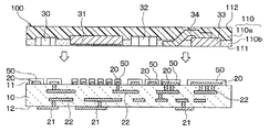
(14th Embodiment)
FIG. 19 is a process diagram showing an alignment process of an electronic device manufacturing method according to a fourteenth embodiment of the present invention, and shows a workpiece in cross section. This embodiment is different from the first embodiment in the configuration of the
図19に示されるように、本実施形態では、用意される樹脂シート110を、その厚さ方向において他面112側に位置する第1の樹脂110aと、一面111側に位置する第2の樹脂110bとが積層された構成としている。
As shown in FIG. 19, in the present embodiment, the
ここで、第1および第2の樹脂110a、110bは共に熱硬化性樹脂であるが、第1の樹脂110aは、第2の樹脂110bよりも硬化温度が低いものである。このような硬化温度の違いは、たとえばエポキシ樹脂などの一般的な熱硬化性樹脂においては、硬化触媒の種類や量を調整することにより容易に実現できる。
Here, the first and
本実施形態では、このような2層の樹脂よりなる樹脂シート110を用いて、電子部品30〜34を埋め込むことにより、シート部材100を形成する。このとき、電子部品30〜34における接続面側の部位は第2の樹脂110bに埋設され、電子部品30〜34における接続面とは反対側の部位は、第1の樹脂110aに埋設されている。
In the present embodiment, the
そして、位置合わせ工程に用いるシート部材100としては、第2の樹脂110bはBステージであり、第1の樹脂110aは完全に硬化したCステージのものを用いる。このことは、上記第1および第2の樹脂110a、110bの硬化温度の相違により、容易に実現できる。
As the
具体的には、両樹脂110a、110bがともにBステージである樹脂シート110を用意し、これに、上記第1実施形態と同様の方法にて、電子部品30〜34を埋め込むようにすればよい。
Specifically, a
そして、このようなシート部材100においては、第1の樹脂110aが完全硬化していることにより、この第1の樹脂110aにより電子部品30〜34が拘束されつつ、電子部品30〜34の接続面側の第2の樹脂110bはBステージであるから、上記各実施形態と同様に、上記封止工程における電子部品30〜34の接続面と基板電極20との電気的接続部の樹脂シート110による封止が容易に行える。
And in such a sheet |
つまり、本実施形態によれば、位置合わせ工程および封止工程において、樹脂シート110のうち第1の樹脂110aによって、電子部品30〜34の位置を確実に固定できるため、当該工程における電子部品30〜34の位置ずれを、より確実に防止することが可能となる。また、本実施形態は、上記各実施形態と組み合わせることができることは、もちろんである。
That is, according to the present embodiment, the positions of the
(他の実施形態)
なお、上記各実施形態では、電子部品30〜34の接続面と基板電極20との電気的接続は、はんだや導電性接着剤などの導電性接合部材50を介して行っていたが、可能ならば、これら電子部品30〜34の接続面と基板電極20とを直接接触させた状態で、固相接合などによる電気的接続を行ってもよい。
(Other embodiments)
In each of the above embodiments, the electrical connection between the connection surfaces of the
また、これも可能ならば、上記したバンプ60を介して接続する場合においても、当該バンプ60と基板電極20との直接接触、あるいは、当該バンプ60と電子部品の接続面との直接接触により、電気的接続を行うようにしてもよい、
また、上記各実施形態では、電子部品は複数であったが、単数でもよく、その場合も、上記各実施形態の効果は発揮されることは、もちろんである。
If this is also possible, even when connecting via the
In each of the above embodiments, there are a plurality of electronic components. However, a single electronic component may be used, and in that case as well, the effect of each of the above embodiments is exhibited.
10 基板
11 基板の一面
12 基板の他面
20 基板電極
30 電子部品
31 電子部品
32 電子部品
33 電子部品
34 電子部品
40 封止樹脂
60 バンプ
100 シート部材
110 樹脂シート
111 樹脂シートの一方の板面
112 樹脂シートの他方の板面
113 凹み
DESCRIPTION OF
Claims (5)
Bステージ状態の熱硬化性樹脂よりなる板状の樹脂シート(110)の内部に前記電子部品(30〜34)を埋め込むとともに、前記電子部品(30〜34)における前記基板電極(20)との接続面を前記樹脂シート(110)の一方の板面(111)にて露出させ、前記樹脂シート(110)の他方の板面(112)に金属シート(80)を貼り付けてなるシート部材(100)と、
前記基板(10)とを用意し、
前記シート部材(100)における前記樹脂シート(110)の一方の板面(111)と前記基板(10)の一面(11)とを対向させて、前記樹脂シート(110)の一方の板面(111)にて露出する前記電子部品(30〜34)の前記接続面と、これに接続される前記基板電極(20)とを位置合わせする位置合わせ工程を行い、
続いて、前記シート部材(100)を前記基板(10)側へ押し付けることにより、前記電子部品(30〜34)の前記接続面と前記基板電極(20)とを電気的に接続するとともに、前記基板電極(20)間にて、前記樹脂シート(110)が、前記基板(10)の一面(11)側へ押し込まれるように変形し、前記基板(10)の一面(11)のうちの前記基板電極(20)の間の部位に貼り付き、前記電子部品(30〜34)の直下部分のうち前記基板電極(20)以外の部位に、変形した前記樹脂シート(110)が回り込むようにすることで、当該接続面と前記基板電極(20)との接続部を前記樹脂シート(110)で封止する封止工程を行い、
その後、前記樹脂シート(110)をその硬化温度以上に加熱して完全に硬化させ、この硬化した前記樹脂シート(110)を前記封止樹脂(40)とする硬化工程を行うことを特徴とする電子装置の製造方法。 An electronic component (30) is mounted on the one surface (11) of the substrate (10) having the substrate electrode (20) on the one surface (11), and the electronic component (30 to 34) and the substrate electrode (20) are mounted. And electrically connecting the electronic components (30-34) with a sealing resin (40) on one surface (11) of the substrate (10),
The electronic component (30-34) is embedded in a plate-shaped resin sheet (110) made of a thermosetting resin in a B-stage state, and the substrate electrode (20) in the electronic component (30-34) is embedded. A sheet member formed by exposing a connection surface at one plate surface (111) of the resin sheet (110) and attaching a metal sheet (80) to the other plate surface (112) of the resin sheet (110). 100)
Preparing the substrate (10);
One plate surface (111) of the resin sheet (110) in the sheet member (100) and one surface (11) of the substrate (10) are opposed to each other, and one plate surface ( 111) performing an alignment step of aligning the connection surfaces of the electronic components (30 to 34) exposed at 111) and the substrate electrodes (20) connected thereto,
Then, by the sheet member (100) pressed into the substrate (10) side, as well as electrically connecting the said connection surface and the substrate electrode of the electronic component (30 to 34) (20), wherein The resin sheet (110) is deformed so as to be pushed into the one surface (11) side of the substrate (10) between the substrate electrodes (20), and the one of the one surfaces (11) of the substrate (10) -out paste at a site between the substrate electrode (20), wherein a part other than the substrate electrode (20) of the portion immediately below the electronic part (30 to 34), wherein the resin sheet (110) such that wrap around the deformed doing, a sealing step of sealing the connection part between the between the connecting surface the substrate electrode (20) in the resin sheet (110),
Thereafter, the resin sheet (110) is heated to a temperature equal to or higher than its curing temperature to be completely cured, and a curing process is performed using the cured resin sheet (110) as the sealing resin (40). A method for manufacturing an electronic device.
前記電子部品(30〜34)の接続面と前記基板電極(20)との接続部は、当該接続面、前記バンプ(60)および前記基板電極(20)により構成されたものとすることを特徴とする請求項1に記載の電子装置の製造方法。 Conductive bumps projecting from one of the connection surfaces of the electronic components (30 to 34) and the substrate electrode (20) connected to the connection surface to the other side connected to the one of the substrate electrodes (20) (60) is provided, and the connection surface and the substrate electrode (20) are electrically connected via the bump (60),
A connection portion between the connection surface of the electronic component (30 to 34) and the substrate electrode (20) is configured by the connection surface, the bump (60), and the substrate electrode (20). A method for manufacturing an electronic device according to claim 1.
前記電子部品(30〜34)の接続面と前記基板電極(20)との接続部は、前記樹脂シート(110)の一方の板面(111)より突出する前記接続面および前記基板電極(20)により構成されたものとすることを特徴とする請求項1または2に記載の電子装置の製造方法。 In the prepared sheet member (100), the connection surface of the electronic components (30 to 34) is left in a state of protruding from one plate surface (111) of the resin sheet (110),
A connection portion between the connection surface of the electronic component (30 to 34) and the substrate electrode (20) includes the connection surface protruding from one plate surface (111) of the resin sheet (110) and the substrate electrode (20). 3. The method of manufacturing an electronic device according to claim 1, wherein:
Priority Applications (1)
| Application Number | Priority Date | Filing Date | Title |
|---|---|---|---|
| JP2010128771A JP5577859B2 (en) | 2010-06-04 | 2010-06-04 | Manufacturing method of electronic device |
Applications Claiming Priority (1)
| Application Number | Priority Date | Filing Date | Title |
|---|---|---|---|
| JP2010128771A JP5577859B2 (en) | 2010-06-04 | 2010-06-04 | Manufacturing method of electronic device |
Related Child Applications (1)
| Application Number | Title | Priority Date | Filing Date |
|---|---|---|---|
| JP2013239737A Division JP5768864B2 (en) | 2013-11-20 | 2013-11-20 | Manufacturing method of electronic device |
Publications (2)
| Publication Number | Publication Date |
|---|---|
| JP2011254047A JP2011254047A (en) | 2011-12-15 |
| JP5577859B2 true JP5577859B2 (en) | 2014-08-27 |
Family
ID=45417716
Family Applications (1)
| Application Number | Title | Priority Date | Filing Date |
|---|---|---|---|
| JP2010128771A Expired - Fee Related JP5577859B2 (en) | 2010-06-04 | 2010-06-04 | Manufacturing method of electronic device |
Country Status (1)
| Country | Link |
|---|---|
| JP (1) | JP5577859B2 (en) |
Families Citing this family (4)
| Publication number | Priority date | Publication date | Assignee | Title |
|---|---|---|---|---|
| JP6055387B2 (en) * | 2013-09-18 | 2016-12-27 | 東京エレクトロン株式会社 | Joining method, program, computer storage medium, and joining system |
| JP2015070034A (en) * | 2013-09-27 | 2015-04-13 | 日東電工株式会社 | Resin sheet and manufacturing method of electronic device package |
| JP6444269B2 (en) | 2015-06-19 | 2018-12-26 | 新光電気工業株式会社 | Electronic component device and manufacturing method thereof |
| CN108039415B (en) * | 2017-11-02 | 2019-06-07 | 厦门市三安光电科技有限公司 | The packaging method of microcomponent |
Family Cites Families (4)
| Publication number | Priority date | Publication date | Assignee | Title |
|---|---|---|---|---|
| JP2004055967A (en) * | 2002-07-23 | 2004-02-19 | Matsushita Electric Ind Co Ltd | Manufacturing method of board with built-in electronic component |
| JP4073830B2 (en) * | 2003-06-20 | 2008-04-09 | 松下電器産業株式会社 | Manufacturing method of semiconductor chip built-in module |
| JP2010010313A (en) * | 2008-06-26 | 2010-01-14 | Murata Mfg Co Ltd | Method of manufacturing substrate with built-in component |
| JP5200870B2 (en) * | 2008-11-12 | 2013-06-05 | 株式会社村田製作所 | Manufacturing method of module with built-in components |
-
2010
- 2010-06-04 JP JP2010128771A patent/JP5577859B2/en not_active Expired - Fee Related
Also Published As
| Publication number | Publication date |
|---|---|
| JP2011254047A (en) | 2011-12-15 |
Similar Documents
| Publication | Publication Date | Title |
|---|---|---|
| TWI400774B (en) | Semiconductor device and manufacturing method of the semiconductor device | |
| JP5579402B2 (en) | Semiconductor device, method for manufacturing the same, and electronic device | |
| JP5198265B2 (en) | Apparatus and method for forming a flat surface of a thin flexible substrate | |
| JP3838331B2 (en) | Semiconductor device and manufacturing method thereof, circuit board, and electronic apparatus | |
| JP4992310B2 (en) | Manufacturing method of laminated substrate | |
| JP2005203497A (en) | Semiconductor device and method for manufacturing same | |
| WO1998025303A1 (en) | Chip scale ball grid array for integrated circuit package | |
| KR20030083553A (en) | Semiconductor device and manufacturing method thereof | |
| WO2009110376A1 (en) | Leadframe substrate, semiconductor module and method for manufacturing leadframe substrate | |
| JP4846633B2 (en) | Manufacturing method of component-embedded substrate | |
| CN100580911C (en) | Circuit module and circuit device using the circuit module | |
| US20090315163A1 (en) | Semiconductor Die Packages with Stacked Flexible Modules Having Passive Components, Systems Using the Same, and Methods of Making the Same | |
| JP5577859B2 (en) | Manufacturing method of electronic device | |
| KR20140100488A (en) | Connection device, method for manufacturing connection structure, method for manufacturing stacked chip component and method for mounting electronic component | |
| US8269343B2 (en) | Semiconductor device including a pressure-contact section | |
| JP2010272556A (en) | Mold package, and method for manufacturing the same | |
| WO2009107342A1 (en) | Method for manufacturing electronic component module | |
| JP6433604B2 (en) | Non-reciprocal circuit device, non-reciprocal circuit device and manufacturing method thereof | |
| KR20040045017A (en) | Semiconductor device and semiconductor device manufacturing method | |
| JP5768864B2 (en) | Manufacturing method of electronic device | |
| JP2012253263A (en) | Semiconductor chip and method of manufacturing the same | |
| JP4062305B2 (en) | Manufacturing method of semiconductor device | |
| JP5056429B2 (en) | Manufacturing method of semiconductor device | |
| JP2012015446A (en) | Method of manufacturing semiconductor device | |
| JP5229200B2 (en) | Manufacturing method of semiconductor device |
Legal Events
| Date | Code | Title | Description |
|---|---|---|---|
| A621 | Written request for application examination |
Free format text: JAPANESE INTERMEDIATE CODE: A621 Effective date: 20120725 |
|
| A977 | Report on retrieval |
Free format text: JAPANESE INTERMEDIATE CODE: A971007 Effective date: 20130328 |
|
| A131 | Notification of reasons for refusal |
Free format text: JAPANESE INTERMEDIATE CODE: A131 Effective date: 20130924 |
|
| TRDD | Decision of grant or rejection written | ||
| A01 | Written decision to grant a patent or to grant a registration (utility model) |
Free format text: JAPANESE INTERMEDIATE CODE: A01 Effective date: 20140610 |
|
| A61 | First payment of annual fees (during grant procedure) |
Free format text: JAPANESE INTERMEDIATE CODE: A61 Effective date: 20140623 |
|
| R151 | Written notification of patent or utility model registration |
Ref document number: 5577859 Country of ref document: JP Free format text: JAPANESE INTERMEDIATE CODE: R151 |
|
| R250 | Receipt of annual fees |
Free format text: JAPANESE INTERMEDIATE CODE: R250 |
|
| R250 | Receipt of annual fees |
Free format text: JAPANESE INTERMEDIATE CODE: R250 |
|
| R250 | Receipt of annual fees |
Free format text: JAPANESE INTERMEDIATE CODE: R250 |
|
| LAPS | Cancellation because of no payment of annual fees |