JP5491969B2 - Transmitter, interface device, in-vehicle communication system - Google Patents
Transmitter, interface device, in-vehicle communication system Download PDFInfo
- Publication number
- JP5491969B2 JP5491969B2 JP2010123950A JP2010123950A JP5491969B2 JP 5491969 B2 JP5491969 B2 JP 5491969B2 JP 2010123950 A JP2010123950 A JP 2010123950A JP 2010123950 A JP2010123950 A JP 2010123950A JP 5491969 B2 JP5491969 B2 JP 5491969B2
- Authority
- JP
- Japan
- Prior art keywords
- transistor
- current
- source
- gate
- voltage
- Prior art date
- Legal status (The legal status is an assumption and is not a legal conclusion. Google has not performed a legal analysis and makes no representation as to the accuracy of the status listed.)
- Active
Links
- 230000006854 communication Effects 0.000 title claims description 16
- 238000004891 communication Methods 0.000 title claims description 16
- 230000005540 biological transmission Effects 0.000 claims description 40
- 239000003990 capacitor Substances 0.000 claims description 40
- 230000005669 field effect Effects 0.000 claims description 23
- 239000004065 semiconductor Substances 0.000 claims description 11
- 238000007599 discharging Methods 0.000 claims description 10
- 239000000758 substrate Substances 0.000 claims description 7
- 230000008054 signal transmission Effects 0.000 claims description 4
- 230000007175 bidirectional communication Effects 0.000 claims description 3
- 238000007667 floating Methods 0.000 claims description 3
- 230000002093 peripheral effect Effects 0.000 claims description 3
- 238000006243 chemical reaction Methods 0.000 claims description 2
- 238000010586 diagram Methods 0.000 description 27
- 230000015556 catabolic process Effects 0.000 description 15
- 238000000034 method Methods 0.000 description 13
- 230000008569 process Effects 0.000 description 11
- 101710170230 Antimicrobial peptide 1 Proteins 0.000 description 9
- 101100464779 Saccharomyces cerevisiae (strain ATCC 204508 / S288c) CNA1 gene Proteins 0.000 description 9
- 230000003071 parasitic effect Effects 0.000 description 7
- 230000007423 decrease Effects 0.000 description 5
- 238000004519 manufacturing process Methods 0.000 description 5
- 238000012986 modification Methods 0.000 description 5
- 230000004048 modification Effects 0.000 description 5
- 230000004044 response Effects 0.000 description 5
- 230000015572 biosynthetic process Effects 0.000 description 2
- 230000008859 change Effects 0.000 description 2
- 238000013461 design Methods 0.000 description 2
- 238000005516 engineering process Methods 0.000 description 2
- 230000000630 rising effect Effects 0.000 description 2
- 210000000746 body region Anatomy 0.000 description 1
- 230000009194 climbing Effects 0.000 description 1
- 238000010276 construction Methods 0.000 description 1
- 238000007796 conventional method Methods 0.000 description 1
- 230000008878 coupling Effects 0.000 description 1
- 238000010168 coupling process Methods 0.000 description 1
- 238000005859 coupling reaction Methods 0.000 description 1
- 230000003247 decreasing effect Effects 0.000 description 1
- 230000001419 dependent effect Effects 0.000 description 1
- 230000000694 effects Effects 0.000 description 1
- 239000012212 insulator Substances 0.000 description 1
- 238000002955 isolation Methods 0.000 description 1
- 229910044991 metal oxide Inorganic materials 0.000 description 1
- 150000004706 metal oxides Chemical class 0.000 description 1
- YMXREWKKROWOSO-VOTSOKGWSA-N methyl (e)-3-(2-hydroxyphenyl)prop-2-enoate Chemical compound COC(=O)\C=C\C1=CC=CC=C1O YMXREWKKROWOSO-VOTSOKGWSA-N 0.000 description 1
- 238000012544 monitoring process Methods 0.000 description 1
- 230000009467 reduction Effects 0.000 description 1
- 229910052710 silicon Inorganic materials 0.000 description 1
- 239000010703 silicon Substances 0.000 description 1
- 238000012546 transfer Methods 0.000 description 1
Images


Classifications
-
- H—ELECTRICITY
- H03—ELECTRONIC CIRCUITRY
- H03K—PULSE TECHNIQUE
- H03K19/00—Logic circuits, i.e. having at least two inputs acting on one output; Inverting circuits
- H03K19/003—Modifications for increasing the reliability for protection
- H03K19/00346—Modifications for eliminating interference or parasitic voltages or currents
- H03K19/00361—Modifications for eliminating interference or parasitic voltages or currents in field effect transistor circuits
Description
本発明は、スルーレート制御機能を備えたトランスミッタ、並びに、これを用いたインタフェイス装置及び車載通信システムに関するものである。 The present invention relates to a transmitter having a slew rate control function, an interface device using the transmitter, and an in-vehicle communication system.
図6は、スルーレート制御機能を備えたトランスミッタの一従来例を示した回路図である。本従来例のトランスミッタにおいて、スイッチ制御部306は、入力信号INの立ち上がりに応じて、スイッチ301をオンとし、スイッチ302をオフとする。このようなスイッチ制御により、コンデンサ305(容量値:C)には、定電流源303からスイッチ301を介して充電電流I1(電流値:+I)が流し込まれる。その結果、コンデンサ305の一端(高電位側)から引き出される出力信号OUTの電圧値は、充電電流I1の電流値とコンデンサ305の容量値に応じた一定のスルーレートSR1(=+I/C[V/s])で上昇し始める。
FIG. 6 is a circuit diagram showing a conventional example of a transmitter having a slew rate control function. In the conventional transmitter, the
また、スイッチ制御部306は、出力信号OUTの電圧値が所定の基準電圧Vrefに達したとき、スイッチ301をオフとする。このようなスイッチ制御により、出力電圧VOUTは、コンデンサ305によりほぼ基準電圧Vrefに維持される。
Further, the
また、スイッチ制御部306は、入力信号INの立ち下がりに応じて、スイッチ301をオフとし、スイッチ302をオンとする。このようなスイッチ制御により、コンデンサ305からは、スイッチ302を介して定電流源304に向けた放電電流I2(電流値:−I)が引き抜かれる。その結果、出力信号OUTの電圧値は、放電電流I2の電流値とコンデンサ305の容量値に応じた一定のスルーレートSR2(=−I/C[V/s])で低下し始める。
Further, the
なお、車載通信システムに関連する従来技術の一例としては、特許文献1を挙げることができる。
Note that
上記従来例のトランスミッタでは、充電電流I1及び放電電流I2の電流値がいずれも固定的に設定されており、延いては、出力信号OUTの立ち上がり時/立ち下り時におけるスルーレートSR1及びSR2がいずれも固定的に設定されていた。そのため、基準電圧Vrefが常に一定であれば、出力信号OUTのライズタイム/フォールタイムは常に一定に維持されるが、基準電圧Vrefが大きく変動する場合には、図7に示すように、出力信号OUTのライズタイム/フォールタイムも大きく変動してしまい、入力信号INと出力信号OUTの間でデューティばらつきを生じるという問題があった。 In the conventional transmitter, the charging current I1 and the discharging current I2 are both fixedly set, and as a result, the slew rates SR1 and SR2 at the rising / falling of the output signal OUT Was also fixedly set. Therefore, if the reference voltage Vref is always constant, the rise time / fall time of the output signal OUT is always kept constant. However, if the reference voltage Vref fluctuates greatly, as shown in FIG. The rise time / fall time of OUT also fluctuates greatly, and there is a problem that duty variation occurs between the input signal IN and the output signal OUT.
本発明は、本願の発明者によって見い出された上記の問題点に鑑み、電源電圧の変動に起因する入力信号と出力信号のデューティばらつきを抑制することが可能なトランスミッタ、並びに、これを用いたインタフェイス装置及び車載通信システムを提供することを目的とする。 In view of the above-described problems found by the inventors of the present application, the present invention provides a transmitter capable of suppressing duty variation between an input signal and an output signal due to fluctuations in power supply voltage, and an interface using the transmitter. An object is to provide a face device and an in-vehicle communication system.
上記目的を達成するために、本発明に係るトランスミッタは、その一端から充電電圧が引き出されるコンデンサと;前記コンデンサの充電電流を生成する第1定電流源と;前記コンデンサの放電電流を生成する第2定電流源と;送信入力信号の論理レベル、及び、前記充電電圧と基準電圧との比較結果に基づいて、前記コンデンサの充放電制御を行う充放電制御部と;前記充電電圧に応じてスルーレートが設定され、出力側電源電圧に応じて信号振幅が設定される送信出力信号を生成する出力段と;前記出力側電源電圧に依存して前記基準電圧を変動させる基準電圧生成部と;前記基準電圧に依存して前記充電電流及び前記放電電流の各電流値を変動させる定電流制御部と;を有する構成(第1の構成)とされている。 To achieve the above object, a transmitter according to the present invention includes a capacitor from which a charging voltage is drawn; a first constant current source that generates a charging current for the capacitor; a first current that generates a discharging current for the capacitor. Two constant current sources; a charge / discharge control unit that performs charge / discharge control of the capacitor based on a logic level of a transmission input signal and a comparison result between the charge voltage and a reference voltage; and through according to the charge voltage An output stage for generating a transmission output signal in which a rate is set and a signal amplitude is set in accordance with an output side power supply voltage; a reference voltage generation unit that varies the reference voltage depending on the output side power supply voltage; A constant current control unit that varies each current value of the charging current and the discharging current depending on a reference voltage (first configuration).
上記第1の構成から成るトランスミッタにおいて、前記出力段は、前記充電電圧に応じて導通度が制御されるオープンドレイン型トランジスタを含む構成(第2の構成)にするとよい。 In the transmitter having the first configuration, the output stage may have a configuration (second configuration) including an open drain transistor whose conductivity is controlled according to the charging voltage.
また、上記第2の構成から成るトランスミッタは、前記オープンドレイン型トランジスタが飽和領域で動作し得る状態になるまで前記放電電流にブースト電流を加え、前記オープンドレイン型トランジスタが飽和領域で動作し得る状態になった時点で前記ブースト電流を切るブースト部をさらに有する構成(第3の構成)にするとよい。 In the transmitter having the second configuration, a boost current is added to the discharge current until the open drain transistor can operate in a saturation region, and the open drain transistor can operate in a saturation region. It is preferable to have a configuration (third configuration) that further includes a boost unit that cuts off the boost current at the point of time.
また、上記第1〜第3いずれかの構成から成るトランスミッタにおいて、前記充放電制御部は、前記コンデンサと前記第1定電流源との間を導通/遮断する第1スイッチと;前記コンデンサと前記第2定電流源との間を導通/遮断する第2スイッチと;前記第1スイッチ及び前記第2スイッチのオン/オフ制御を行うスイッチ制御部と;を含む構成(第4の構成)にするとよい。 Further, in the transmitter having any one of the first to third configurations, the charge / discharge control unit includes a first switch that conducts / cuts off between the capacitor and the first constant current source; A configuration (fourth configuration) including: a second switch that conducts / cuts off between the second constant current source; and a switch control unit that performs on / off control of the first switch and the second switch. Good.
また、上記第1〜第4いずれかの構成から成るトランスミッタにおいて、前記基準電圧生成部は、前記出力側電源電圧を分圧して前記基準電圧を生成する抵抗ラダーである構成(第5の構成)にするとよい。 In the transmitter having any one of the first to fourth configurations, the reference voltage generation unit is a resistor ladder that divides the output-side power supply voltage to generate the reference voltage (fifth configuration). It is good to.
また、上記第1〜第5いずれかの構成から成るトランスミッタにおいて、前記定電流制御部は、前記基準電圧を電圧/電流変換して基準電流を生成する基準電流生成部と;前記基準電流を前記充電電流及び前記放電電流として複製するカレントミラー部と;を含む構成(第6の構成)にするとよい。 Further, in the transmitter having any one of the first to fifth configurations, the constant current control unit includes a reference current generation unit configured to generate a reference current by performing voltage / current conversion on the reference voltage; And a current mirror section that replicates as the charging current and the discharging current (sixth configuration).
また、上記第2の構成から成るトランスミッタにおいて、前記出力段は、アノードが前記送信出力信号の出力端に接続され、カソードが前記オープンドレイン型トランジスタのドレインに接続されたダイオードを含む構成(第7の構成)にするとよい。 In the transmitter having the second configuration, the output stage includes a diode having an anode connected to the output terminal of the transmission output signal and a cathode connected to the drain of the open drain transistor (seventh). (Configuration).
また、上記第7の構成から成るトランスミッタにおいて、前記ダイオードは、半導体基板上の一領域に形成された埋め込み絶縁層と、前記埋め込み絶縁層の上部周縁上に形成されたコレクタウォールと、によって取り囲まれたフローティング領域内に形成されている構成(第8の構成)にするとよい。 In the transmitter having the seventh configuration, the diode is surrounded by a buried insulating layer formed in a region on the semiconductor substrate and a collector wall formed on the upper peripheral edge of the buried insulating layer. It is preferable to adopt a configuration (eighth configuration) formed in the floating region.
また、上記第7または第8の構成から成るトランスミッタにおいて、前記出力段は、前記オープンドレイン型トランジスタのドレインと前記ダイオードのカソードとの間に接続されたDMOS電界効果トランジスタを含む構成(第9の構成)にするとよい。 Further, in the transmitter having the seventh or eighth configuration, the output stage includes a DMOS field effect transistor connected between a drain of the open drain transistor and a cathode of the diode (a ninth configuration). Configuration).
また、本発明に係るインタフェイス装置は、信号送信経路に設けられた上記第1〜第9いずれかの構成から成るトランスミッタと;信号受信経路に設けられたレシーバと;を有する構成(第10の構成)にするとよい。 In addition, an interface apparatus according to the present invention includes: a transmitter having any one of the first to ninth configurations provided in the signal transmission path; and a receiver provided in the signal reception path. Configuration).
なお、上記第10の構成から成るインタフェイス装置において、前記レシーバは、互いのソースが共通接続されて、一方のドレインから受信出力信号が引き出される一対の第1トランジスタ及び第2トランジスタと;ゲートが受信入力信号の入力端に接続され、ソースが第1トランジスタのゲートに接続された第3トランジスタと;ゲートが受信基準電圧の入力端に接続され、ソースが第2トランジスタのゲートに接続された第4トランジスタと;カソードが前記第1トランジスタのゲートに接続され、アノードが前記第1トランジスタのソースに接続された第1ツェナダイオードと;カソードが前記第2トランジスタのゲートに接続され、アノードが前記第2トランジスタのソースに接続された第2ツェナダイオードと;カソードが前記第3トランジスタのゲートに接続され、アノードが前記第3トランジスタのソースに接続された第3ツェナダイオードと;カソードが前記第4トランジスタのゲートに接続され、アノードが前記第4トランジスタのソースに接続された第4ツェナダイオードと;前記第1トランジスタと前記第2トランジスタのソース電流を生成する第1電流源と;前記第3トランジスタのソース電流を生成する第2電流源と;前記第4トランジスタのソース電流を生成する第3電流源と;を含む構成(第11の構成)にするとよい。 In the interface device having the tenth configuration, the receiver includes a pair of first and second transistors whose sources are connected in common and a reception output signal is drawn from one drain; A third transistor having a source connected to the input terminal of the reception reference voltage and a source connected to the input terminal of the reception reference voltage; a source connected to the gate of the second transistor; Four transistors; a first Zener diode having a cathode connected to the gate of the first transistor and an anode connected to a source of the first transistor; a cathode connected to the gate of the second transistor, and an anode connected to the first transistor A second Zener diode connected to the source of two transistors; A third Zener diode connected to the gate of the transistor and having an anode connected to the source of the third transistor; a cathode connected to the gate of the fourth transistor; and an anode connected to the source of the fourth transistor. 4 Zener diodes; a first current source that generates source currents of the first transistor and the second transistor; a second current source that generates source currents of the third transistor; and a source current of the fourth transistor A third current source to be generated may be included (an eleventh configuration).
また、上記第11の構成から成るインタフェイス装置において、前記レシーバは、前記第1トランジスタのゲートと前記第3トランジスタのソースとの間に挿入された電流制限抵抗をさらに含む構成(第12の構成)にするとよい。 Further, in the interface device having the eleventh configuration, the receiver further includes a current limiting resistor inserted between the gate of the first transistor and the source of the third transistor (twelfth configuration). ).
また、上記第10の構成から成るインタフェイス装置において、前記レシーバは、互いのソースが共通接続され、一方のドレインから受信出力信号が引き出される一対の第1トランジスタ及び第2トランジスタと;カソードが前記第1トランジスタのゲートに接続され、アノードが前記第1トランジスタのソースに接続された第1ツェナダイオードと;カソードが前記第2トランジスタのゲートに接続され、アノードが前記第2トランジスタのソースに接続された第2ツェナダイオードと;前記第1トランジスタと前記第2トランジスタのソース電流を生成する電流源と;アノードが前記第1トランジスタのソースに接続され、カソードが前記電流源に接続された第1ダイオードと;アノードが前記第2トランジスタのソースに接続され、カソードが前記電流源に接続された第2ダイオードと;を含む構成(第13の構成)にするとよい。 In the interface device having the tenth configuration, the receiver has a pair of first and second transistors whose sources are connected in common and a reception output signal is drawn from one drain; A first Zener diode connected to the gate of the first transistor and having an anode connected to the source of the first transistor; a cathode connected to the gate of the second transistor; and an anode connected to the source of the second transistor. A second Zener diode; a current source for generating a source current of the first transistor and the second transistor; a first diode having an anode connected to a source of the first transistor and a cathode connected to the current source And the anode is connected to the source of the second transistor, Better to configure containing (Configuration 13); over de and a second diode connected to the current source.
また、上記第13の構成から成るインタフェイス装置において、前記第1ダイオード及び前記第2ダイオードは、ダイオード接続されたpnp型バイポーラトランジスタである構成(第14の構成)にするとよい。 In the interface device having the thirteenth configuration, the first diode and the second diode may be a diode-connected pnp bipolar transistor (fourteenth configuration).
また、本発明に係る車載通信システムは、ECUと;バスと;前記ECUと前記バスとの双方向通信を仲介する上記第10〜第14いずれかの構成から成るインタフェイス装置と;を有する構成(第15の構成)とされている。 Further, an in-vehicle communication system according to the present invention includes an ECU, a bus, and an interface device having any one of the tenth to fourteenth configurations that mediate bidirectional communication between the ECU and the bus. (Fifteenth configuration).
本発明に係るトランスミッタ、並びに、これを用いたインタフェイス装置及び車載通信システムによれば、電源電圧の変動に起因する入力信号と出力信号のデューティばらつきを抑制することが可能となる。 According to the transmitter according to the present invention, the interface device using the transmitter, and the in-vehicle communication system, it is possible to suppress the duty variation of the input signal and the output signal due to the fluctuation of the power supply voltage.
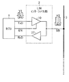
(車載通信システムのブロック図)
図1は、車載通信システムの一構成例を示すブロック図である。本図に例示した車載通信システムは、ECU[Electronic Control Unit]1と、LIN[Local Interconnect Network]インターフェイス部2と、LINバス3と、を有する。
(Block diagram of in-vehicle communication system)
FIG. 1 is a block diagram illustrating a configuration example of an in-vehicle communication system. The in-vehicle communication system illustrated in this figure includes an ECU [Electronic Control Unit] 1, a LIN [Local Interconnect Network]
ECU1は、車両に搭載されている各種デバイスの制御主体となるマイクロコンピュータユニットである。特に、LINバス3に接続されるECU1は、それほど高速な応答性を必要としないデバイス(操作部、ドアミラー駆動部、パワーウィンドウ駆動部など)に組み込まれるものである。
The ECU 1 is a microcomputer unit that is a main control body of various devices mounted on the vehicle. In particular, the
LINインタフェイス部2は、ECU1とLINバス3との双方向通信を仲介するインタフェイス装置であり、トランスミッタ10とレシーバ20を有する。トランスミッタ10は、ECU1からLINバス3への信号送信経路上に設けられており、ECU1から入力される送信データTxDをバス信号SBとしてLINバス3に出力する。レシーバ20は、LINバス3からECU1への信号受信経路上に設けられており、LINバス3から入力されるバス信号SBを受信データRxDとしてECU1に出力する。なお、トランスミッタ10及びレシーバ20の構成及び動作については、後ほど詳細に説明を行う。
The
LINバス3にバス信号SBを出力するときには、ECU1からトランスミッタ10に入力されるイネーブル制御信号ENが出力許可状態を示す論理レベルとされ、トランスミッタ10の出力段が出力許可状態とされる。一方、LINバス3からバス信号SBを受信するときには、イネーブル制御信号ENが出力禁止状態を示す論理レベルとされ、トランスミッタ10の出力段が出力禁止状態(ハイインピーダンス状態)とされる。
When the bus signal SB is output to the
なお、ECU1(3V系や5V系など)で取り扱われる送信データTxDや受信データRxDは、ハイレベルをECU側電源電圧V1とし、ローレベルをグランド電圧としてスイングされる小振幅信号(例えば、ハイレベルが2V以下、ローレベルが0.8V以下として規定されているLVTTL[Low Voltage Transistor Transistor Logic]信号)である。一方、バス信号SBは、オープンドレイン型トランジスタなどを用いて、ハイレベルをバス側電源電圧V2(例えば5V〜27V)とし、ローレベルをグランド電圧としてスイングされる大振幅信号である。つまり、トランスミッタ10及びレシーバ20には、いずれも、レベルシフタ機能が備えられている。また、トランスミッタ10には、スルーレート制御機能も備えられている。
The transmission data TxD and reception data RxD handled by the ECU 1 (3V system, 5V system, etc.) are small amplitude signals (for example, high level) that are swung with the high level as the ECU-side power supply voltage V1 and the low level as the ground voltage. Is an LVTTL (Low Voltage Transistor Transistor Logic) signal defined as 2 V or less and a low level of 0.8 V or less. On the other hand, the bus signal SB is a large-amplitude signal that is swung using an open drain transistor or the like with the high level as the bus-side power supply voltage V2 (for example, 5 V to 27 V) and the low level as the ground voltage. That is, both the
LINバス3は、CAN[Controller Area Network]やFlexRayに比べて、それほど広い帯域幅や多用途性が要求されていない車載通信ネットワーク(LIN)の構築に用いられる低コストのシリアル信号伝送ラインである。LINバス3では、LINマスタと1つまたは複数のLINスレーブから成るマスタ/スレーブ方式が採用されている。なお、LINバス3を介してやり取りされるバス信号SBの転送レートは、非常に小さい(最大20kb/s)。
The
(トランスミッタの概略的構成)
図2は、トランスミッタ10の概略的構成を示す回路図である。本構成例のトランスミッタ10は、スイッチ101及び102と、定電流源103及び104と、コンデンサ105と、スイッチ制御部106と、基準電圧生成部107と、定電流制御部108と、アンプ109と、Nチャネル型MOS[Metal Oxide Semiconductor]電界効果トランジスタ110〜112と、Pチャネル型MOS電界効果トランジスタ113及び114と、抵抗115及び116と、を有する。
(Schematic configuration of transmitter)
FIG. 2 is a circuit diagram showing a schematic configuration of the
スイッチ101は、スイッチ制御部106からの指示に基づいて、コンデンサ105と定電流源103との間を導通/遮断する。スイッチ102は、スイッチ制御部106からの指示に基づいて、コンデンサ105と定電流源104との間を導通/遮断する。
The
定電流源103は、コンデンサ105の充電電流I1を生成する。なお、定電流源103の一端はECU側電源電圧V1の印加端に接続されており、他端はスイッチ101に接続されている。定電流源104は、コンデンサ105の放電電流I2を生成する。なお、定電流源104の一端はスイッチ102に接続されており、他端は接地端に接続されている。コンデンサ105は、その一端(高電位端)から充電電圧Vaが引き出される。
The constant
スイッチ制御部106は、ECU側電源電圧V1の入力を受けて動作し、送信入力信号IN(図1の送信データTxDに相当)の論理レベル、及び、充電電圧Vaと基準電圧Vrefとの比較結果に基づいて、スイッチ101及び102のオン/オフ制御を行う。例えば、スイッチ101をオンとし、スイッチ102をオフとすれば、コンデンサ105に充電電流I1を流し込む状態となる。逆に、スイッチ101をオフとし、スイッチ102をオンとすれば、コンデンサ105から放電電流I2を引き込む状態となる。また、コンデンサ105に充電電圧Vaが蓄えられている状態で、スイッチ101及び102をいずれもオフとすれば、コンデンサ105の充電電圧Vaを維持する状態となる。すなわち、スイッチ101及び102と、スイッチ制御部106によって、コンデンサ105の充放電制御を行う充放電制御部が形成されている。なお、充放電制御部(101、102、及び、106)の構成及び動作については、後ほど具体的に説明する。
The
基準電圧生成部107は、バス側電源電圧V2に依存して基準電圧Vrefを変動させる。定電流制御部108は、ECU側電源電圧V1の入力を受けて動作し、基準電圧Vrefに依存して充電電流I1及び放電電流I2の各電流値を変動させる。なお、基準電圧生成部107、及び、定電流制御部108の構成及び動作については、後ほど具体的に説明する。
The reference
アンプ109、トランジスタ110〜114、並びに、抵抗115及び116は、トランスミッタ10の出力段を形成する回路要素である。アンプ109の非反転入力端(+)は、充電電圧Vaの印加端(コンデンサ105の高電位端)に接続されている。アンプ109の反転入力端(−)は、抵抗115の第1端に接続されている。アンプ109の出力端は、トランジスタ110のゲートに接続されている。アンプ109の上側電源端は、ECU側電源電圧V1の入力端に接続されている。アンプ109の下側電源端は、接地端に接続されている。トランジスタ110のソース及びバックゲートは、いずれも抵抗115の第1端に接続されている。抵抗115の第2端は接地端に接続されている。トランジスタ110のドレインは、トランジスタ113のドレインに接続されている。トランジスタ113及び114のソース及びバックゲートは、いずれもECU側電源電圧V1の印加端に接続されている。トランジスタ113及び114のゲートは、いずれもトランジスタ113のソースに接続されている。トランジスタ114のドレインは、トランジスタ111のドレインに接続されている。トランジスタ111及び112のソース及びバックゲートは、いずれも接地端に接続されている。トランジスタ111及び112のゲートはいずれもトランジスタ111のドレインに接続されている。トランジスタ112のドレインは、送信出力信号OUT(図1のバス信号SBに相当)の出力端に接続されるとともに、抵抗116を介してバス側電源電圧V2の印加端にも接続されている。
The
アンプ109は、抵抗115(抵抗値:R115)の第1端に印加される電圧が充電電圧Vaと一致するように、トランジスタ110のゲート信号を帰還制御する。従って、トランジスタ113に流れる電流I3は、充電電圧Vaに比例した電流値(最大値:Vref/R115)を持つことになる。トランジスタ113と114はカレントミラー(ミラー比1:1)を形成しており、電流I3はトランジスタ114に流れる電流I4として複製される。従って、電流I4についても充電電圧Vaに比例した電流値(最大値:Vref/R115)を持つことになる。また、トランジスタ111と112はカレントミラー(ミラー比1:1)を形成しており、電流I4の電流値に応じてトランジスタ112のゲート電圧が変動する。より具体的には、電流I4の電流値が大きいほど、トランジスタ112のゲート電圧が高くなり、延いては、トランジスタ112の導通度が大きくなる。すなわち、トランジスタ112は、充電電圧Vaに応じて導通度が制御されるオープンドレイン型トランジスタであると言うことができる。従って、トランジスタ112のドレインから引き出される送信出力信号OUTは、そのスルーレートが充電電圧Vaに応じて設定され、その信号振幅がバス側電源電圧V2に応じて設定されることになる。
The
(トランスミッタ前段部分の具体的構成)
図3は、トランスミッタ10(前段部分に設けられた充電電圧Vaの生成機能部)の具体的構成を示す回路図である。
(Specific configuration of transmitter front part)
FIG. 3 is a circuit diagram showing a specific configuration of the transmitter 10 (a function unit for generating the charging voltage Va provided in the preceding stage).
スイッチ101としては、Pチャネル型MOS電界効果トランジスタP1が用いられている。スイッチ102としては、Nチャネル型MOS電界効果トランジスタN1が用いられている。定電流源103としては、Pチャネル型MOS電界効果トランジスタP2が用いられている。定電流源104としては、Nチャネル型MOS電界効果トランジスタN2が用いられている。
As the
トランジスタP1のソース及びバックゲートは、トランジスタP2のドレインに接続されている。トランジスタP2のソース及びバックゲートは、ECU側電源電圧V1の印加端に接続されている。トランジスタP1及びN1のドレインは、充電電圧Vaの印加端に接続されている。トランジスタN1のソース及びバックゲートは、トランジスタN2のドレインに接続されている。トランジスタN2のソース及びバックゲートは、接地端に接続されている。 The source and back gate of the transistor P1 are connected to the drain of the transistor P2. The source and back gate of the transistor P2 are connected to the application end of the ECU side power supply voltage V1. The drains of the transistors P1 and N1 are connected to the application end of the charging voltage Va. The source and back gate of the transistor N1 are connected to the drain of the transistor N2. The source and back gate of the transistor N2 are connected to the ground terminal.
スイッチ制御部106は、コンパレータCMP1と、論理和演算器OR1と、を含んでいる。コンパレータCMP1の非反転入力端(+)は、充電電圧Vaの印加端に接続されている。コンパレータCMP1の反転入力端(−)は、基準電圧Vrefの印加端に接続されている。コンパレータCMP1の上側電源端は、ECU側電源電圧V1の印加端に接続されている。コンパレータCMP1の下側電源端は、接地端に接続されている。論理和演算器OR1の第1入力端は、コンパレータCMP1の出力端に接続されている。論理和演算器OR1の第2入力端は、送信入力信号INの入力端に接続されている。なお、送信信号INの入力端は、トランジスタN1のゲートにも接続されている。論理和演算器OR1の出力端は、トランジスタP1のゲートに接続されている。論理和演算器OR1の上側電源端は、ECU側電源電圧V1の印加端に接続されている。論理和演算器OR1の下側電源端は、接地端に接続されている。
The
基準電圧生成部107は、バス側電源電圧V2と接地端との間に直列接続され、その接続ノードから基準電圧Vrefが引き出される抵抗R1及びR2を含んでいる。つまり、基準電圧生成部107としては、バス側電源電圧V2を所定の分圧比α(=R2/(R1+R2)、例えばα=1/2)で分圧することにより、基準電圧Vref(=α×V2)を生成する抵抗ラダーが採用されている。このような構成であれば、極めて容易に、バス側電源電圧V2に依存(比例)して基準電圧Vrefを変動させることが可能となる。
The
定電流制御部108は、アンプAMP1と、Nチャネル型MOS電界効果トランジスタN3及びN4と、Pチャネル型MOS電界効果トランジスタP3及びP4と、抵抗R3とを含んでいる。アンプAMP1の非反転入力端(+)は、基準電圧Vrefの印加端に接続されている。アンプAMP1の反転入力端(−)は、抵抗R3の第1端に接続されている。アンプAMP1の出力端は、トランジスタN3のゲートに接続されている。アンプAMP1の上側電源端は、ECU側電源電圧V1の入力端に接続されている。アンプAMP1の下側電源端は、接地端に接続されている。トランジスタN3のソース及びバックゲートは、いずれも抵抗R3の第1端に接続されている。抵抗R3の第2端は、接地端に接続されている。トランジスタN3のドレインは、トランジスタP3のドレインに接続されている。トランジスタP3及びP4のソース及びバックゲートは、いずれもECU側電源電圧V1の印加端に接続されている。トランジスタP2〜P4のゲートは、いずれもトランジスタN3のソースに接続されている。トランジスタP4のドレインは、トランジスタN4のドレインに接続されている。トランジスタN4のソース及びバックゲートは、接地端に接続されている。トランジスタN2及びN4のゲートは、いずれもトランジスタN4のソースに接続されている。
The constant
アンプAMP1は、抵抗R3の第1端に印加される電圧が基準電圧Vrefと一致するように、トランジスタN3のゲート信号を帰還制御する。従って、トランジスタP3に流れる基準電流I0は、基準電圧Vref(延いてはバス側電源電圧V2)に比例した電流値I(=Vref/R3=(α×V2)/R3)を持つことになる。トランジスタP2とP3はカレントミラー(ミラー比1:1)を形成しており、基準電流I0はトランジスタP2に流れる充電電流I1として複製される。また、トランジスタP3とP4、及び、トランジスタN2とN4は、それぞれカレントミラー(ミラー比1:1)を形成しており、基準電流I0はトランジスタN2に流れる放電電流I2として複製される。 The amplifier AMP1 feedback-controls the gate signal of the transistor N3 so that the voltage applied to the first terminal of the resistor R3 matches the reference voltage Vref. Therefore, the reference current I0 flowing through the transistor P3 has a current value I (= Vref / R3 = (α × V2) / R3) proportional to the reference voltage Vref (and thus the bus-side power supply voltage V2). The transistors P2 and P3 form a current mirror (mirror ratio 1: 1), and the reference current I0 is duplicated as the charging current I1 flowing through the transistor P2. The transistors P3 and P4 and the transistors N2 and N4 form a current mirror (mirror ratio 1: 1), respectively, and the reference current I0 is duplicated as a discharge current I2 flowing through the transistor N2.
すなわち、定電流制御部108は、基準電圧Vrefを電圧/電流変換して基準電流I0を生成する基準電流生成部(AMP1、N3、及び、R3)と、基準電流I0を充電電流I1及び放電電流I2として複製するカレントミラー部(P3、P4、及び、N4)とを含んでいると言うことができる。
In other words, the constant
(トランスミッタの動作説明)
図4は、図2及び図3の構成から成るトランスミッタ10の動作を説明するための信号波形図であり、上から順に、送信入力信号IN、コンパレータCMP1の比較信号Scmp、トランジスタP1のゲート信号G1、トランジスタN1のゲート信号G2(送信入力信号INと同一)、充電電圧Va、及び、送信出力信号OUTが描写されている。
(Description of transmitter operation)
FIG. 4 is a signal waveform diagram for explaining the operation of the
時刻t11以前には、送信入力信号INがハイレベルに維持されており、出力信号OUTがハイレベル(=バス側電源電圧V2)に維持されているものとする。 Prior to time t11, it is assumed that the transmission input signal IN is maintained at a high level and the output signal OUT is maintained at a high level (= bus side power supply voltage V2).
時刻t11において、送信入力信号INがハイレベルからローレベルに立ち下げられると、ゲート信号G1及びG2はいずれもローレベルに立ち下げられる。その結果、トランジスタP1がオンとなり、トランジスタN1がオフとなる。このようなスイッチ制御により、コンデンサ105(容量値:C)には、トランジスタP2からトランジスタP1を介して充電電流I1(電流値:+I)が流し込まれる。その結果、コンデンサ105の一端(高電位側)から引き出される充電電圧Vaは、充電電流I1の電流値とコンデンサ105の容量値に応じた一定のスルーレートSR1(=+I/C[V/s])で上昇を開始する。このとき、充電電圧Vaは基準電圧Vrefに達していないため、比較信号Scmpはローレベルに維持されたままとなる。また、出力段に流れる電流I3及びI4は、いずれも充電電圧Vaに比例した電流値を持ち、トランジスタ112の導通度は、充電電圧Vaの上昇に伴って大きくなっていくので、送信出力信号OUTは、それまでのハイレベル(=バス側電源電圧V2)から一定のスルーレートSR3で低下し始める。すなわち、送信出力信号OUTの立ち下がり時におけるスルーレートSR3は、充電電圧Vaに応じて設定されることになる。
When the transmission input signal IN falls from the high level to the low level at time t11, both the gate signals G1 and G2 fall to the low level. As a result, the transistor P1 is turned on and the transistor N1 is turned off. By such switch control, the charging current I1 (current value: + I) flows into the capacitor 105 (capacitance value: C) from the transistor P2 via the transistor P1. As a result, the charging voltage Va drawn from one end (high potential side) of the
その後、時刻t12において、充電電圧Vaが基準電圧Vrefに達したとき、比較信号Scmpがローレベルからハイレベルに立ち上がるので、論理和回路OR1から出力されるゲート信号G1は、送信入力信号INの論理レベルに依ることなく、ハイレベルに立ち上げられる。その結果、トランジスタP1がオフとなり、充電電圧Vaは、コンデンサ105によりほぼ基準電圧Vrefに維持される。なお、比較信号Scmpの論理レベルが意図せず切り替わらないように、コンパレータCMP1には、ヒステリシス特性を持たせておくことが望ましい。また、時刻t12の時点で、送信出力信号OUTはローレベル(=0V近傍)まで低下している。
After that, when the charging voltage Va reaches the reference voltage Vref at time t12, the comparison signal Scmp rises from the low level to the high level, so that the gate signal G1 output from the OR circuit OR1 is the logic level of the transmission input signal IN. It is launched at a high level without depending on the level. As a result, the transistor P1 is turned off, and the charging voltage Va is maintained at the reference voltage Vref by the
その後、時刻t13において、送信入力信号INがローレベルからハイレベルに立ち上げられると、ゲート信号G1及びG2はいずれもハイレベル(ゲート信号G1は時刻t13以前からハイレベル)に立ち上げられる。その結果、トランジスタP1がオフに維持され、トランジスタN1がオンとなる。このようなスイッチ制御により、コンデンサ105からは、トランジスタN1を介してトランジスタN2に放電電流I2(電流値:−I)が引き抜かれる。その結果、充電電圧Vaは、放電電流I2の電流値とコンデンサ105の容量値に応じた一定のスルーレートSR2(=−I/C[V/s])で低下し始める。このとき、比較信号Scmpはハイレベルからローレベルに立ち下げられる。また、出力段を形成するトランジスタ112の導通度は、充電電圧Vaの低下に伴って小さくなっていくので、送信出力信号OUTは、それまでのローレベル(=0V近傍)から一定のスルーレートSR4で上昇し始める。すなわち、送信出力信号OUTの立ち上がり時におけるスルーレートSR4は、充電電圧Vaに応じて設定されることになる。
Thereafter, when the transmission input signal IN is raised from the low level to the high level at time t13, both the gate signals G1 and G2 are raised to the high level (the gate signal G1 is raised to the high level before time t13). As a result, the transistor P1 is kept off and the transistor N1 is turned on. By such switch control, the discharge current I2 (current value: -I) is drawn from the
その後、時刻t14において、出力段を形成するトランジスタ112の導通度がゼロとなり、送信出力信号OUTがハイレベル(=バス側電源電圧V2)に達する。また、この時点でコンデンサ105は完全に放電されており、充電電圧Vaは0Vとなっている。この状態は、時刻t11以前の状態と同一であり、時刻t15において、送信入力信号INがハイレベルからローレベルに立ち下げられると、上記と同様の動作が繰り返される。
After that, at time t14, the conductivity of the
ここで、重要となるポイントは、バス側電源電圧V2に依存して基準電圧Vrefを変動させるとともに、基準電圧Vref(延いてはバス側電源電圧V2)に依存して基準電流I0(延いては充電電流I1及び放電電流I2)を変動させることにより、充電電圧VaのスルーレートSR1及びSR2(延いては送信出力信号OUTのスルーレートSR3及びSR4)にV2依存性を持たせた点である(図4中の実線と破線を比較参照)。 Here, the important point is that the reference voltage Vref is changed depending on the bus-side power supply voltage V2, and the reference current I0 (and thus extended) depending on the reference voltage Vref (and thus the bus-side power supply voltage V2). By varying the charging current I1 and the discharging current I2), the slew rates SR1 and SR2 of the charging voltage Va (and hence the slew rates SR3 and SR4 of the transmission output signal OUT) are made V2 dependent ( Compare the solid line and the broken line in FIG. 4).
このような構成とすることにより、基準電圧Vrefと基準電流I0(延いては充電電流I1及び放電電流I2)との間で互いのV2依存性が相殺される。従って、バッテリの充電状況や車載デバイスの駆動状況などに応じてバス側電源電圧V2(出力信号OUTの信号振幅)が大きく変動したとしても、充電電圧Va(延いては送信出力信号OUT)のライズタイム/フォールタイムT(=C×Vref/I=C×R3)を常に一定に維持することができるので、送信入力信号INと送信出力信号OUTとの間のデューティばらつきを低減することが可能となる。 With such a configuration, the mutual V2 dependency is canceled between the reference voltage Vref and the reference current I0 (and thus the charging current I1 and the discharging current I2). Therefore, even if the bus-side power supply voltage V2 (signal amplitude of the output signal OUT) varies greatly depending on the battery charging status, the driving status of the in-vehicle device, etc., the charging voltage Va (and thus the transmission output signal OUT) rises. Since the time / fall time T (= C × Vref / I = C × R3) can always be kept constant, it is possible to reduce the duty variation between the transmission input signal IN and the transmission output signal OUT. Become.
また、上記の構成であれば、上記の演算式(T=C×Vref/I=C×R3)に基づいて、容易に所望のライズタイム/フォールタイムTを設定することが可能である。例えば、ライズタイム/フォールタイムTを長くしたければ、充電電圧VaのスルーレートSR1及びSR2を小さくすればよいので、抵抗R3の抵抗値を大きくして基準電流I0を小さくするか、或いは、コンデンサ105の容量値Cを大きくすればよい。逆に、ライズタイム/フォールタイムTを短くしたければ、充電電圧VaのスルーレートSR1及びSR2を大きくすればよいので、抵抗R3の抵抗値を小さくして基準電流I0を大きくするか、或いは、コンデンサ105の容量値Cを小さくすればよい。
Also, with the above configuration, it is possible to easily set a desired rise time / fall time T based on the arithmetic expression (T = C × Vref / I = C × R3). For example, if the rise time / fall time T is to be increased, the slew rates SR1 and SR2 of the charging voltage Va may be reduced, so that the resistance value of the resistor R3 is increased to reduce the reference current I0, or the capacitor The capacitance value C of 105 may be increased. Conversely, if the rise time / fall time T is to be shortened, the slew rates SR1 and SR2 of the charging voltage Va may be increased, so that the resistance value of the resistor R3 is decreased to increase the reference current I0, or The capacitance value C of the
また、上記のスルーレート制御機能を備えたLINインタフェイス部2であれば、車両毎に異なるバス側電源電圧V2を考慮することなく汎用的に適用することができるので、LINインタフェイス部2(または、これが組み込まれた車載デバイス)の生産性を高めて、そのコストダウンに貢献することが可能となる。
Further, the
なお、上記のスルーレート制御技術は、本実施形態で例示されている車載通信システムだけでなく、送信信号のデューティ精度が重要となる全てのアプリケーションの信頼性を高める上で有用である。 The above slew rate control technique is useful not only for improving the reliability of not only the in-vehicle communication system exemplified in this embodiment but also all applications in which the duty accuracy of the transmission signal is important.
(トランスミッタの変形例)
次に、トランスミッタ10の変形例について図5を参照しながら説明する。図5は、トランスミッタ10(後段部分)の一変形例を示す回路図である。
(Transmitter variation)
Next, a modification of the
LINの標準規格では、3種類の負荷(500Ω/10nF、660Ω/6.8nF、1000Ω/1nF)を接続することが可能である。しかしながら、LINバス3に接続される負荷の特性が変化すると、トランスミッタ10で生成される送信出力信号OUTのスルーレートSR3及びSR4に意図しない変動が生じるおそれがあり、特に、負荷が重い場合には、送信出力信号OUTの立ち上がりが鈍ってしまう。
In the LIN standard, three types of loads (500Ω / 10 nF, 660Ω / 6.8 nF, 1000Ω / 1 nF) can be connected. However, if the characteristics of the load connected to the
そこで、本変形例のトランスミッタ10は、出力段を形成するオープンドレイン型トランジスタ112が飽和領域で動作し得る状態になるまで放電電流I2にブースト電流Ibstを加え、オープンドレイン型トランジスタ112が飽和領域で動作し得る状態になった時点、すなわち、トランジスタ112のドレイン・ソース間電圧Vdsがトランジスタ112のゲート・ソース間電圧Vgsからトランジスタ112のオンスレッショルド電圧Vthを差し引いた値よりも大きくなった時点で、ブースト電流Ibstを切るブースト部BSTをさらに有する構成とされている。
Therefore, the
ブースト部BSTは、Nチャネル型MOS電界効果トランジスタ117と、定電流源118及び119と、スイッチ120と、コンパレータ121と、を有する。トランジスタ117は、トランジスタ112と同一のオンスレッショルド電圧Vthを有するように、トランジスタ112と同一の製造プロセスで形成されたモニタ用トランジスタである。定電流源118は、トランジスタ112に僅かな電流(例えば100nA)を流す。定電流源119は、ブースト電流Ibstを生成する。スイッチ120は、ブースト電流Ibstの流れる電流経路を導通/遮断する。コンパレータ121は、トランジスタ117のソースから引き出される電圧信号Vx(=Vgs−Vth)と、トランジスタ112のドレインから引き出される電圧信号Vy(=Vds)とを比較し、その比較結果に基づいてスイッチ120のオン/オフ制御を行う。
The boost unit BST includes an N-channel MOS
各回路要素の接続関係について具体的に説明する。トランジスタ117のドレインは、ECU側電源電圧V1の印加端に接続されている。トランジスタ117のソース及びバックゲートは、いずれもコンパレータ121の反転入力端(−)と、定電流源118の第1端に接続されている。トランジスタ117のゲートは、トランジスタ111及び112のゲートと共に、トランジスタ111のドレインに接続されている。定電流源118の第2端は、接地端に接続されている。コンパレータ121の非反転入力端(+)は、トランジスタ112のドレイン(送信出力信号OUTの出力端)に接続されている。コンパレータ121の出力端は、スイッチ120の制御端に接続されている。コンパレータ121の上側電源端は、ECU側電源電圧V1の印加端に接続されている。コンパレータ121の下側電源端は、接地端に接続されている。スイッチ120の第1端はスイッチ102と定電流源104との接続ノードに接続されている。スイッチ120の第2端は、定電流源118の第1端に接続されている。定電流源118の第2端は、接地端に接続されている。
The connection relationship of each circuit element will be specifically described. The drain of the
上記構成から成るブースト部BSTにおいて、トランジスタ117のゲートには、トランジスタ112のゲート・ソース間電圧Vgsが印加されている。また、先にも述べた通り、トランジスタ117は、トランジスタ112と同一のオンスレッショルド電圧Vthを有するように、トランジスタ112と同一の製造プロセスで形成されている。従って、トランジスタ112と共にトランジスタ117がオンされるとき、トランジスタ117のドレインから引き出される電圧信号Vxは、トランジスタ112のゲート・ソース間電圧Vgsからトランジスタ112のオンスレッショルド電圧Vthを差し引いた値となる。一方、トランジスタ112のドレインから引き出される電圧信号Vyは、トランジスタ112のドレイン・ソース間電圧Vdsに相当する。従って、コンパレータ121は、トランジスタ112のVdsと(Vgs−Vth)とを比較している形となり、延いては、トランジスタ112が飽和領域で動作し得る状態となったか否かを判定している形となる。
In the boost unit BST configured as described above, the gate-source voltage Vgs of the
従って、トランジスタ112が飽和領域で動作し得る状態になるまでは、放電電流I2にブースト電流Ibstを加えたブースト放電電流I2’でコンデンサ105の放電を行い、トランジスタ112が飽和領域で動作し得る状態になった時点で、ブースト電流Ibstを切るようにコンパレータ121の出力に応じてスイッチ120のオン/オフ制御を行うことにより、LINバス3に接続される負荷が重い場合であっても、送信出力信号OUT(バス信号SB)の立ち上がりが鈍らないので、所望のスルーレートを維持することが可能となる。
Therefore, until the
(オープンドレイン出力段の耐圧向上)
図8は、オープンドレイン出力段の第1構成例を示す回路図であり、図2や図5のオープンドレイン出力段のみを改めて描写し直したものである。図8に示すように、トランジスタ112のドレイン・ソース間には、寄生ダイオードDpが付随している。そのため、送信出力信号OUTの出力端に負電位のサージが入力された場合には、接地端から寄生ダイオードDpを介する経路で大量の順方向電流が流れ、トランジスタ112が破壊する恐れがある。
(Improved breakdown voltage of open drain output stage)
FIG. 8 is a circuit diagram showing a first configuration example of the open drain output stage, in which only the open drain output stage of FIGS. 2 and 5 is redrawn. As shown in FIG. 8, a parasitic diode Dp is attached between the drain and source of the
図9は、オープンドレイン出力段の第2構成例を示す回路図である。上記した負電位のサージに対する耐性を高めるべく、第2構成例のオープンドレイン出力段は、アノードが送信出力信号OUTの出力端に接続され、カソードがトランジスタ112のドレインに接続されたダイオード122を含む構成とされている。このような構成とすることにより、送信出力信号OUTの出力端に負電位のサージが入力された場合であっても、接地端から寄生ダイオードDpを介する経路は、逆バイアス状態のダイオード122によって遮断されるため、寄生ダイオードDpに大量の順方向電流が流れることはなく、トランジスタ112の破壊を防止することが可能となる。
FIG. 9 is a circuit diagram showing a second configuration example of the open drain output stage. In order to enhance the resistance against the negative potential surge described above, the open drain output stage of the second configuration example includes a
なお、半導体装置の製造プロセスとして、SOI[Silicon On Insulator]プロセスが採用されている場合には、回路素子を形成するためのエピタキシャル成膜層と半導体基板(GND)とが中間絶縁層で完全に分離されているので、上記のダイオード122を容易に形成することが可能である。しかしながら、半導体装置の製造プロセスとして、より安価で一般的なCMOSプロセスやBiCMOSプロセスを採用する場合には、半導体基板とダイオード122との間に生じる寄生素子により、ダイオード122の挿入によって本来得られるべき耐圧性能が十全に機能しなくなる。そのため、このような問題を解消するためには、ダイオード122の構造に工夫を凝らす必要がある。
When an SOI [Silicon On Insulator] process is employed as a semiconductor device manufacturing process, the epitaxial film formation layer for forming circuit elements and the semiconductor substrate (GND) are completely separated by an intermediate insulating layer. Therefore, the
図10は、ダイオード122の模式的構造を示す縦断面図である。本構造のダイオード122は、p−型の半導体基板P−sub上の一領域に形成されたn+型の埋め込み絶縁層B/L[Burried Layer]と、埋め込み絶縁層B/Lの上部周縁上に形成されたn−型のコレクタウォールC/W[Collector Wall]と、によって取り囲まれたフローティング領域内に形成されている。このような構造を採用することにより、ダイオード122を半導体基板P−subから電気的に分離することができるので、半導体基板P−subとダイオード122との間に寄生素子を生じることがなくなり、ダイオード122の挿入によって本来得られるべき耐圧性能を十全に機能させることが可能となる。
FIG. 10 is a longitudinal sectional view showing a schematic structure of the
なお、図10に描写された他の符号について簡単に説明する。L/I及び1stLIはp−型の低絶縁層[Low Isolation]、Epiはn−型のエピタキシャル成膜層、Pwellはp+型のウェル領域、及び、NBodyはn+型のボディ領域を各々示している。 The other symbols depicted in FIG. 10 will be briefly described. L / I and 1stLI are p-type low insulating layers [Low Isolation], Epi is an n-type epitaxial film formation layer, Pwell is a p + type well region, and NBody is an n + type body region. .
図11は、オープンドレイン出力段の第3構成例を示す回路図である。図9のダイオード122を挿入することにより、オープンドレイン出力段の負電位耐圧を高めることはできるが、送信出力信号OUTの出力端に正電位のサージが入力された場合には、ダイオード122が順バイアス状態となるため、トランジスタ112のドレイン・ソース間耐圧を十分高く設計しておかない限り、トランジスタ112が破壊する恐れがある。しかしながら、CMOSプロセスで形成されているオープンドレイン出力段のうち、トランジスタ112のみを高耐圧なDMOSプロセスで形成すると、カレントミラーを形成するトランジスタ111とトランジスタ112とのカップリング特性(ミラー比のばらつき特性)が悪化し、スルーレート制御が困難となってしまう。
FIG. 11 is a circuit diagram showing a third configuration example of the open drain output stage. Although the negative potential withstand voltage of the open drain output stage can be increased by inserting the
そこで、第3構成例のオープンドレイン出力段は、CMOSプロセスで形成されたトランジスタ112のドレインとダイオード122のカソードとの間に接続されたDMOSプロセスで形成されたNチャネル型MOS電界効果トランジスタ123を含む構成とされている。すなわち、第3構成例のオープンドレイン出力段では、その正電位耐圧を高めるために、ドレイン・ソース間耐圧の高いトランジスタ123がソースフォロワとして用いられている。このような構成とすることにより、トランジスタ112をCMOSプロセスで形成したまま、オープンドレイン出力段の正電位耐性を高めることが可能となる。
Therefore, the open drain output stage of the third configuration example includes an N-channel MOS
なお、トランジスタ123のゲートには、トランジスタ112を常に飽和領域で動作させ得るだけのバイアス電圧BIAS(≧VgsC−VthC+VgsD)が与えられている。なお、上記パラメータのうち、VgsCはトランジスタ112のゲート・ソース間電圧、VthCはトランジスタ112のオンスレッショルド電圧、VgsDはトランジスタ123のゲート・ソース間電圧を示している。このようなバイアス電圧BIASを印加しておけば、LINバス3に接続される負荷の状態に依らず、トランジスタ112を常に飽和領域で動作させることができるので、図5で示したブースト部BSTが不要となる。
Note that a bias voltage BIAS (≧ VgsC−VthC + VgsD) that can always operate the
また、図9〜図11に示した構成ないし構造を全て実現する場合であっても、半導体装置の製造プロセスとしては、SOIプロセスよりも安価で一般的なBiCDMOSプロセスを採用することが可能である。従って、高価なSOIプロセスを用いることなく、正電位サージ及び負電位サージの双方に対して高耐圧なオープンドレイン出力段を実現することが可能となる。 Even when all the configurations and structures shown in FIGS. 9 to 11 are realized, it is possible to employ a general BiCDMOS process which is cheaper than the SOI process and is used as a semiconductor device manufacturing process. . Therefore, an open drain output stage having a high withstand voltage against both positive potential surge and negative potential surge can be realized without using an expensive SOI process.
特に、LINインタフェイス部2には、正負双方の高耐圧(例えば−27V〜40V)が要求されているので、上記のオープンドレイン出力段を採用することにより、この要求に応えることが可能となる。
In particular, since the
ただし、上記の高耐圧化技術は、本実施形態で例示されている車載通信システムだけでなく、高サージ耐性を必要とするNチャネル型オープンドレイン出力段全般に適用することが可能であることは言うまでもない。 However, the high withstand voltage technology described above can be applied not only to the in-vehicle communication system exemplified in this embodiment but also to all N-channel open drain output stages that require high surge resistance. Needless to say.
(レシーバの構成例)
図12は、レシーバ20の第1構成例を示す回路図である。第1構成例のレシーバ20は、Nチャネル型電界効果トランジスタ201及び202と、抵抗203及び204と、定電流源205と、レベルシフタ206と、を有する。
(Example of receiver configuration)
FIG. 12 is a circuit diagram illustrating a first configuration example of the
トランジスタ201及び202のドレインは、それぞれ抵抗203及び204を介してバス側電源電圧V2の印加端に接続されている。トランジスタ201及び202のソース及びバックゲートは、いずれも定電流源205を介して接地端に接続されている。トランジスタ201のゲートは、受信入力信号RIN(図1のバス信号SBに相当)の入力端に接続されている。トランジスタ202のゲートは、受信基準電圧VREFの入力端に接続されている。レベルシフタ206の入力端は、トランジスタ202のドレインに接続されている。レベルシフタ206の出力端は、受信出力信号ROUT(図1の受信データRxDに相当)の出力端に接続されている。
The drains of the
なお、レベルシフタ206は、トランジスタ202のドレインから引き出される電圧信号(ハイレベルをバス側電源電圧V2とし、ローレベルをグランド電圧としてスイングされる大振幅信号)の入力を受け、これを受信出力信号ROUT(ハイレベルをECU側電源V1とし、ローレベルをグランド電圧としてスイングされる小振幅信号)に変換する。
The
しかしながら、第1構成例のレシーバ20では、トランジスタ201のゲートに入力される受信入力信号RINがバス側電源電圧V2となったときに、トランジスタ201及び202のソースには、バス側電源電圧V2からトランジスタ201のゲート・ソース間電圧Vgs1を差し引いたソース電圧(V2−Vgs1)が現れる。そのため、トランジスタ202のゲート・ソース間には、上記のソース電圧(V2−Vgs1)から受信基準電圧VREFを差し引いたゲート・ソース間電圧(V2−Vgs1−REF)が印加されるため、これがトランジスタ202のゲート・ソース間耐圧を超えていると、トランジスタ202が破壊されてしまうおそれがある。
However, in the
図13は、レシーバ20の第2構成例を示す回路図である。第2構成例のレシーバ20は、第1構成例の回路要素201〜206に加えて、Nチャネル型MOS電界効果トランジスタ207及び208と、定電流源209及び210と、ツェナダイオード211〜214と、抵抗215と、を有する。
FIG. 13 is a circuit diagram illustrating a second configuration example of the
トランジスタ207のドレインは、バス側電源電圧V2の印加端に接続されている。トランジスタ207のソースとバックゲートは、いずれも定電流源209を介して接地端に接続される一方、抵抗215を介してトランジスタ201のゲートにも接続されている。トランジスタ207のゲートは、トランジスタ201のゲートに代わる形で、受信入力信号RINの入力端に接続されている。トランジスタ208のドレインは、バス側電源電圧V2の印加端に接続されている。トランジスタ208のソースとバックゲートは、いずれも定電流源210を介して接地端に接続される一方、トランジスタ202のゲートにも接続されている。トランジスタ208のゲートは、トランジスタ202のゲートに代わる形で、受信基準電圧VREFの入力端に接続されている。
The drain of the
ツェナダイオード211のカソードはトランジスタ201のゲートに接続されている。ツェナダイオード211のアノードは、トランジスタ201のソースに接続されている。ツェナダイオード212のカソードは、トランジスタ202のゲートに接続されている。ツェナダイオード212のアノードは、トランジスタ202のソースに接続されている。ツェナダイオード213のカソードは、トランジスタ207のゲートに接続されている。ツェナダイオード213のアノードは、トランジスタ207のソースに接続されている。ツェナダイオード214のカソードは、トランジスタ208のゲートに接続されている。ツェナダイオード214のアノードは、トランジスタ208のソースに接続されている。
The cathode of the
すなわち、第2構成例のレシーバ20は、互いのソースが共通接続されて、一方のドレインから受信出力信号ROUTが引き出される一対のトランジスタ201及び202と;ゲートが受信入力信号RINの入力端に接続され、ソースがトランジスタ201のゲートに接続されたトランジスタ207と;ゲートが受信基準電圧VREFの入力端に接続されて、ソースがトランジスタ202のゲートに接続されたトランジスタ208と;カソードがトランジスタ201のゲートに接続され、アノードがトランジスタ201のソースに接続されたツェナダイオード211と;カソードがトランジスタ202のゲートに接続されて、アノードがトランジスタ202のソースに接続されたツェナダイオード212と;カソードがトランジスタ207のゲートに接続されて、アノードがトランジスタ207のソースに接続されたツェナダイオード213と;カソードがトランジスタ208のゲートに接続されて、アノードがトランジスタ208のソースに接続されたツェナダイオード214と;トランジスタ201とトランジスタ202のソース電流を生成する定電流源205と;トランジスタ207のソース電流を生成する定電流源209と;トランジスタ208のソース電流を生成する定電流源210と;を含む構成とされている。
That is, the
なお、ツェナダイオード211〜214のツェナ電圧は、いずれもNチャネル型MOS電界効果トランジスタ201、202、207、及び、208のゲート・ソース間耐圧を超えない値(=5V程度)に設計されている。
Note that the Zener voltages of the
このように、トランジスタ対を形成するトランジスタ201及び202とは別に、ソースフォロワとして用いられるトランジスタ207及び208を用意し、受信入力信号RINと受信基準電圧VREFをそれぞれトランジスタ207及び208のゲートに入力した上で、さらに、トランジスタ201、202、207、及び、208のゲート・ソース間に、各々のクランプ素子としてツェナダイオード211〜214を接続することにより、トランジスタ201、202、207、及び208の各ゲート・ソース間電圧が各々の設計耐圧を超えないレベルでクランプされるので、トランジスタの破壊を未然に防止することが可能となり、延いては、第1構成例のレシーバ20よりもバス側電源電圧V2のダイナミックレンジを広げることが可能となる。また、トランジスタ201及び202として高耐圧、低速度の素子を用いる必要がなくなるので、LINインタフェイス部2の高速化に貢献することが可能となる。
As described above, the
また、第2構成例のレシーバ20は、トランジスタ201のゲートとトランジスタ207のソースとの間に挿入された電流制限抵抗をさらに含む構成とされている。このような構成とすることにより、受信入力信号RINの入力端から、降伏したツェナダイオード213及び211を経た後、順バイアス状態のツェナダイオード212及び214を介して受信基準電圧VREFの入力端に至る電流経路、若しくは、その逆に、受信基準電圧VREFの入力端から、降伏したツェナダイオード214及び212を経た後、順バイアス状態のツェナダイオード211及び213を介して受信入力信号RINの入力端に至る電流経路に流れる電流を抑制することが可能となる。
Further, the
図14は、レシーバ20の第3構成例を示す回路図である。第3構成例のレシーバ20は、第1構成例の回路要素201〜206に加えて、ツェナダイオード211及び212と、ダイオード216及び217と、を有する。
FIG. 14 is a circuit diagram illustrating a third configuration example of the
ツェナダイオード211のカソードはトランジスタ201のゲートに接続されている。ツェナダイオード211及びダイオード216のアノードは、いずれもトランジスタ201のソースに接続されている。ツェナダイオード212のカソードは、トランジスタ202のゲートに接続されている。ツェナダイオード212及びダイオード217のアノードは、いずれもトランジスタ202のソースに接続されている。ダイオード216及び217のカソードは、定電流源205に共通接続されている。
The cathode of the
すなわち、第2構成例のレシーバ20は、互いのソースが共通接続され、一方のドレインから受信出力信号ROUTが引き出される一対のトランジスタ201及び202と;カソードがトランジスタ201のゲートに接続されて、アノードがトランジスタ201のソースに接続されたツェナダイオード211と;カソードがトランジスタ202のゲートに接続されて、アノードがトランジスタ202のソースに接続されたツェナダイオード212と;トランジスタ201とトランジスタ202のソース電流を生成する定電流源205と;アノードがトランジスタ201のソースに接続され、カソードが定電流源205に接続されたダイオード216と;アノードがトランジスタ202のソースに接続され、カソードが定電流源205に接続されたダイオード217と;を含む構成とされている。
That is, the
このように、トランジスタ201及び202のゲート・ソース間に、各々のクランプ素子としてツェナダイオード211及び212を接続することにより、第2構成例と同様、トランジスタ201及び202の各ゲート・ソース間電圧が各々の設計耐圧を超えないレベルでクランプされるので、トランジスタの破壊を未然に防止することが可能となる。
In this way, by connecting the
また、トランジスタ201及び202の各ソースと定電流源205との間に、ダイオード216及び217を挿入することにより、受信入力信号RINの入力端から降伏したツェナダイオード211と順バイアス状態のダイオード216を介して受信基準電圧VREFの入力端に至る電流経路上には、逆バイアス状態のトランジスタ217が挿入された形となり、その逆に、受信基準電圧VREFの入力端から降伏したツェナダイオード212と順バイアス状態のダイオード217を介して受信入力信号RINの入力端に至る電流経路上には、逆バイアス状態のトランジスタ216が挿入された形となるため、各々の電流経路に流れる電流を完全に遮断することが可能となる。
Further, by inserting the
すなわち、第3構成例のレシーバ20であれば、第2構成例よりも少ない素子数で、これと同等以上の作用効果を享受することが可能となる。
In other words, with the
また、第3構成例のレシーバ20において、ダイオード216及び217は、図15に示すように、ダイオード接続されたpnp型バイポーラトランジスタで形成することが望ましい。なぜなら、pnp型バイポーラトランジスタのベース・コレクタ間における順方向耐圧は非常に高い(50V程度)ので、大きな逆バイアス電圧が印加されたとしてもブレイクされることなく、これが挿入された電流経路を確実に遮断することが可能となる。
Further, in the
特に、LINインタフェイス部2には、正負双方の高耐圧(例えば−27V〜40V)が要求されているので、上記のレシーバ20を採用することにより、この要求に応えることが可能となる。
In particular, since the
ただし、上記の高耐圧化技術は、本実施形態で例示されている車載通信システムだけでなく、大振幅の信号を受信する必要のあるレシーバ全般に適用することが可能であることは言うまでもない。 However, it goes without saying that the high withstand voltage technology described above can be applied not only to the in-vehicle communication system exemplified in the present embodiment but also to all receivers that need to receive a signal with a large amplitude.
(その他の変形例)
また、本発明の構成は、上記実施形態のほか、発明の主旨を逸脱しない範囲で種々の変更を加えることが可能である。すなわち、上記実施形態は、全ての点で例示であって、制限的なものではないと考えられるべきであり、本発明の技術的範囲は、上記実施形態の説明ではなく、特許請求の範囲によって示されるものであり、特許請求の範囲と均等の意味及び範囲内に属する全ての変更が含まれると理解されるべきである。
(Other variations)
The configuration of the present invention can be variously modified within the scope of the present invention in addition to the above embodiment. That is, the above-described embodiment is an example in all respects and should not be considered as limiting, and the technical scope of the present invention is not the description of the above-described embodiment, but the claims. It should be understood that all modifications that come within the meaning and range of equivalents of the claims are included.
本発明は、例えば、車載通信システムの信頼性を高めるために有用な技術である。 The present invention is a useful technique for increasing the reliability of an in-vehicle communication system, for example.
1 ECU
2 LINインタフェイス部
3 LINバス
4 操作部
5 ドアミラー駆動部
6 パワーウィンドウ駆動部
10 トランスミッタ
20 レシーバ
101、102 スイッチ
103、104 定電流源
105 コンデンサ
106 スイッチ制御部
107 基準電圧生成部
108 定電流制御部
109 アンプ
110〜112 Nチャネル型MOS電界効果トランジスタ
113、114 Pチャネル型MOS電界効果トランジスタ
115、116 抵抗
117 Nチャネル型MOS電界効果トランジスタ
118、119 定電流源
120 スイッチ
121 コンパレータ
122 ダイオード
123 Nチャネル型DMOS電界効果トランジスタ
201、202 Nチャネル型MOS電界効果トランジスタ
203、204 抵抗
205 定電流源
206 レベルシフタ
207、208 Nチャネル型MOS電界効果トランジスタ
209、210 定電流源
211〜214 ツェナダイオード
215 抵抗
216、217 ダイオード
N1〜N4 Nチャネル型MOS電界効果トランジスタ
P1〜P4 Pチャネル型MOS電界効果トランジスタ
R1〜R4 抵抗
AMP1 アンプ
CMP1 コンパレータ
OR1 論理和演算器
BST ブースト部
Dp 寄生ダイオード
1 ECU
2
Claims (15)
前記コンデンサの充電電流を生成する第1定電流源と;
前記コンデンサの放電電流を生成する第2定電流源と;
送信入力信号の論理レベル、及び、前記充電電圧と基準電圧との比較結果に基づいて、前記コンデンサの充放電制御を行う充放電制御部と;
前記充電電圧に応じて論理レベルが切り替わる送信出力信号を生成する出力段と;
前記送信出力信号の信号振幅に相当する出力側電源電圧に依存して前記基準電圧を変動させる基準電圧生成部と;
前記基準電圧に依存して前記充電電流及び前記放電電流の各電流値を変動させる定電流制御部と;
を有することを特徴とするトランスミッタ。 A capacitor from which the charging voltage is drawn from one end;
A first constant current source for generating a charging current for the capacitor;
A second constant current source for generating a discharge current of the capacitor;
A charge / discharge control unit that performs charge / discharge control of the capacitor based on a logic level of a transmission input signal and a comparison result between the charge voltage and a reference voltage;
An output stage for generating a transmission output signal whose logic level switches according to the charging voltage;
A reference voltage generator that varies the reference voltage depending on an output-side power supply voltage corresponding to the signal amplitude of the transmission output signal ;
A constant current control unit that varies each current value of the charging current and the discharging current depending on the reference voltage;
A transmitter characterized by comprising:
前記コンデンサと前記第1定電流源との間を導通/遮断する第1スイッチと;
前記コンデンサと前記第2定電流源との間を導通/遮断する第2スイッチと;
前記第1スイッチ及び前記第2スイッチのオン/オフ制御を行うスイッチ制御部と;
を含むことを特徴とする請求項1〜請求項3のいずれかに記載のトランスミッタ。 The charge / discharge control unit
A first switch for conducting / cutting off between the capacitor and the first constant current source;
A second switch for conducting / cutting off between the capacitor and the second constant current source;
A switch control unit that performs on / off control of the first switch and the second switch;
The transmitter according to any one of claims 1 to 3, further comprising:
前記基準電圧を電圧/電流変換して基準電流を生成する基準電流生成部と;
前記基準電流を前記充電電流及び前記放電電流として複製するカレントミラー部と;
を含むことを特徴とする請求項1〜請求項5のいずれかに記載のトランスミッタ。 The constant current controller is
A reference current generator for generating a reference current by performing voltage / current conversion on the reference voltage;
A current mirror unit that replicates the reference current as the charging current and the discharging current;
The transmitter according to claim 1, comprising:
信号受信経路に設けられたレシーバと;
を有することを特徴とするインタフェイス装置。 A transmitter according to any one of claims 1 to 9 provided in a signal transmission path;
A receiver provided in the signal receiving path;
An interface device comprising:
互いのソースが共通接続され、一方のドレインから受信出力信号が引き出される一対の第1トランジスタ及び第2トランジスタと;
ゲートが受信入力信号の入力端に接続され、ソースが第1トランジスタのゲートに接続された第3トランジスタと;
ゲートが受信基準電圧の入力端に接続され、ソースが第2トランジスタのゲートに接続された第4トランジスタと;
カソードが前記第1トランジスタのゲートに接続され、アノードが前記第1トランジスタのソースに接続された第1ツェナダイオードと;
カソードが前記第2トランジスタのゲートに接続され、アノードが前記第2トランジスタのソースに接続された第2ツェナダイオードと;
カソードが前記第3トランジスタのゲートに接続され、アノードが前記第3トランジスタのソースに接続された第3ツェナダイオードと;
カソードが前記第4トランジスタのゲートに接続され、アノードが前記第4トランジスタのソースに接続された第4ツェナダイオードと;
前記第1トランジスタと前記第2トランジスタのソース電流を生成する第1電流源と;
前記第3トランジスタのソース電流を生成する第2電流源と;
前記第4トランジスタのソース電流を生成する第3電流源と;
を含むことを特徴とする請求項10に記載のインタフェイス装置。 The receiver is
A pair of first and second transistors whose sources are connected in common and from which one of the drains receives a received output signal;
A third transistor having a gate connected to the input end of the received input signal and a source connected to the gate of the first transistor;
A fourth transistor having a gate connected to the input end of the received reference voltage and a source connected to the gate of the second transistor;
A first Zener diode having a cathode connected to the gate of the first transistor and an anode connected to the source of the first transistor;
A second Zener diode having a cathode connected to the gate of the second transistor and an anode connected to the source of the second transistor;
A third Zener diode having a cathode connected to the gate of the third transistor and an anode connected to the source of the third transistor;
A fourth Zener diode having a cathode connected to the gate of the fourth transistor and an anode connected to the source of the fourth transistor;
A first current source for generating a source current of the first transistor and the second transistor;
A second current source for generating a source current of the third transistor;
A third current source for generating a source current of the fourth transistor;
The interface device according to claim 10, comprising:
互いのソースが共通接続され、一方のドレインから受信出力信号が引き出される一対の第1トランジスタ及び第2トランジスタと;
カソードが前記第1トランジスタのゲートに接続され、アノードが前記第1トランジスタのソースに接続された第1ツェナダイオードと;
カソードが前記第2トランジスタのゲートに接続され、アノードが前記第2トランジスタのソースに接続された第2ツェナダイオードと;
前記第1トランジスタと前記第2トランジスタのソース電流を生成する電流源と;
アノードが前記第1トランジスタのソースに接続され、カソードが前記電流源に接続された第1ダイオードと;
アノードが前記第2トランジスタのソースに接続され、カソードが前記電流源に接続された第2ダイオードと;
を含むことを特徴とする請求項10に記載のインタフェイス装置。 The receiver is
A pair of first and second transistors whose sources are connected in common and from which one of the drains receives a received output signal;
A first Zener diode having a cathode connected to the gate of the first transistor and an anode connected to the source of the first transistor;
A second Zener diode having a cathode connected to the gate of the second transistor and an anode connected to the source of the second transistor;
A current source for generating a source current of the first transistor and the second transistor;
A first diode having an anode connected to the source of the first transistor and a cathode connected to the current source;
A second diode having an anode connected to the source of the second transistor and a cathode connected to the current source;
The interface device according to claim 10, comprising:
バスと;
前記ECUと前記バスとの双方向通信を仲介する請求項10〜請求項14のいずれかに記載のインタフェイス装置と;
を有することを特徴とする車載通信システム。 With ECU;
With bus;
The interface device according to any one of claims 10 to 14, which mediates bidirectional communication between the ECU and the bus;
An in-vehicle communication system characterized by comprising:
Priority Applications (3)
| Application Number | Priority Date | Filing Date | Title |
|---|---|---|---|
| JP2010123950A JP5491969B2 (en) | 2010-05-31 | 2010-05-31 | Transmitter, interface device, in-vehicle communication system |
| US13/113,235 US8410827B2 (en) | 2010-05-31 | 2011-05-23 | Transmitter, interface device, and car mounted communication system |
| CN201110142968.4A CN102290982B (en) | 2010-05-31 | 2011-05-30 | Transmitter, interface device, and car mounted communication system |
Applications Claiming Priority (1)
| Application Number | Priority Date | Filing Date | Title |
|---|---|---|---|
| JP2010123950A JP5491969B2 (en) | 2010-05-31 | 2010-05-31 | Transmitter, interface device, in-vehicle communication system |
Publications (3)
| Publication Number | Publication Date |
|---|---|
| JP2011250345A JP2011250345A (en) | 2011-12-08 |
| JP2011250345A5 JP2011250345A5 (en) | 2013-07-04 |
| JP5491969B2 true JP5491969B2 (en) | 2014-05-14 |
Family
ID=45021591
Family Applications (1)
| Application Number | Title | Priority Date | Filing Date |
|---|---|---|---|
| JP2010123950A Active JP5491969B2 (en) | 2010-05-31 | 2010-05-31 | Transmitter, interface device, in-vehicle communication system |
Country Status (3)
| Country | Link |
|---|---|
| US (1) | US8410827B2 (en) |
| JP (1) | JP5491969B2 (en) |
| CN (1) | CN102290982B (en) |
Families Citing this family (27)
| Publication number | Priority date | Publication date | Assignee | Title |
|---|---|---|---|---|
| WO2011160305A1 (en) * | 2010-06-25 | 2011-12-29 | 北京中星微电子有限公司 | Ac-dc power supply converter and current modulation circuit therein |
| US8860398B2 (en) * | 2011-02-11 | 2014-10-14 | Fairchild Semiconductor Corporation | Edge rate control gate driver for switching power converters |
| TW201306416A (en) * | 2011-07-28 | 2013-02-01 | Raydium Semiconductor Corp | Electric apparatus with ESD protection effect |
| CN103684400B (en) * | 2012-09-25 | 2017-04-05 | 联咏科技股份有限公司 | Interface circuit |
| US8742803B2 (en) * | 2012-09-26 | 2014-06-03 | Broadcom Corporation | Output driver using low voltage transistors |
| US8848770B2 (en) * | 2012-12-17 | 2014-09-30 | Em Microelectronic-Marin S.A. | Automatic gain control unit for a low power receiver or transceiver |
| JP6013214B2 (en) * | 2013-02-04 | 2016-10-25 | ルネサスエレクトロニクス株式会社 | Bus communication transceiver |
| JP6065737B2 (en) | 2013-05-10 | 2017-01-25 | 株式会社ソシオネクスト | Output circuit and voltage signal output method |
| JP2015015643A (en) * | 2013-07-05 | 2015-01-22 | ローム株式会社 | Signal transmission circuit |
| JP6296535B2 (en) | 2013-12-09 | 2018-03-20 | ローム株式会社 | Diode and signal output circuit including the same |
| CN103684398B (en) * | 2013-12-26 | 2016-08-31 | 中国科学院上海微系统与信息技术研究所 | A kind of anti-EMI filter LIN bus signals driver |
| CN104900199B (en) * | 2014-03-05 | 2017-08-15 | 矽创电子股份有限公司 | Driving module and display device thereof |
| KR102182572B1 (en) * | 2014-04-15 | 2020-11-25 | 삼성디스플레이 주식회사 | Interface circuit |
| CN104202024B (en) * | 2014-08-29 | 2017-06-30 | 杭州士兰微电子股份有限公司 | It is adapted to the open-drain circuit on the floating ground of high pressure |
| JP2017118185A (en) * | 2015-12-21 | 2017-06-29 | 富士電機株式会社 | Semiconductor integrated circuit |
| CN106788392B (en) * | 2017-01-09 | 2023-05-09 | 四川埃姆克伺服科技有限公司 | Single-ended analog input interface circuit for servo controller |
| CN108732462B (en) * | 2018-04-12 | 2020-02-21 | 华为技术有限公司 | Detection device and method |
| CN109546999B (en) * | 2018-11-28 | 2022-11-15 | 中国电子科技集团公司第四十七研究所 | Programmable USB current-limiting switch |
| JP2021013142A (en) * | 2019-07-09 | 2021-02-04 | 株式会社村田製作所 | Power amplifier circuit |
| US11164784B2 (en) | 2019-08-22 | 2021-11-02 | Micron Technology, Inc. | Open-drain transistor monitoring circuit in a multi-chip package to control power |
| US10884480B1 (en) | 2019-08-22 | 2021-01-05 | Micron Technology, Inc. | Current summing monitoring circuit in a multi-chip package to control power |
| US11237612B2 (en) | 2019-08-22 | 2022-02-01 | Micron Technology, Inc. | Charge-sharing capacitive monitoring circuit in a multi-chip package to control power |
| TWI773968B (en) * | 2020-03-02 | 2022-08-11 | 瑞昱半導體股份有限公司 | Transmitter circuit and operation method |
| CN113381774B (en) * | 2020-03-09 | 2022-07-19 | 瑞昱半导体股份有限公司 | Transmitting circuit and working method thereof |
| US10938387B1 (en) * | 2020-06-24 | 2021-03-02 | Cypress Semiconductor Corporation | Local interconnect network (LIN) driver circuit |
| WO2024053216A1 (en) * | 2022-09-08 | 2024-03-14 | ローム株式会社 | Signal transmitting apparatus |
| WO2024053217A1 (en) * | 2022-09-08 | 2024-03-14 | ローム株式会社 | Signal transmission device |
Family Cites Families (15)
| Publication number | Priority date | Publication date | Assignee | Title |
|---|---|---|---|---|
| JPS5160142A (en) * | 1974-10-25 | 1976-05-25 | Nippon Electric Co | CHOKURYUZOFUKUKI |
| JPS61118010A (en) * | 1984-11-14 | 1986-06-05 | Mitsubishi Electric Corp | Semiconductor integrated circuit |
| ATE100256T1 (en) * | 1987-06-29 | 1994-01-15 | Digital Equipment Corp | BUS TRANSMITTER WITH CONTROLLED, TRAPEZOIDAL OUTPUT VOLTAGE. |
| JPS6451710A (en) * | 1987-08-21 | 1989-02-28 | Mitsubishi Electric Corp | Voltage controlled oscillation circuit |
| JPH07221568A (en) * | 1994-02-09 | 1995-08-18 | Fuji Electric Co Ltd | Amplifier circuit device |
| JP2000323973A (en) * | 1999-05-06 | 2000-11-24 | Nec Corp | Output slew rate control circuit |
| DE19962523A1 (en) * | 1999-12-23 | 2001-08-02 | Texas Instruments Deutschland | DC voltage converter and method for operating a DC voltage converter |
| US6459602B1 (en) * | 2000-10-26 | 2002-10-01 | O2 Micro International Limited | DC-to-DC converter with improved transient response |
| WO2006102927A1 (en) * | 2005-04-01 | 2006-10-05 | Freescale Semiconductor, Inc. | Charge pump and control scheme |
| CN101449451B (en) * | 2006-08-28 | 2011-07-20 | 半导体元件工业有限责任公司 | A charge pump controller and a method thereof |
| JP4630381B2 (en) * | 2007-05-30 | 2011-02-09 | パナソニック株式会社 | Spread spectrum control PLL circuit and startup method thereof |
| CN101420223B (en) * | 2007-10-23 | 2012-05-23 | 三星电子株式会社 | Differential transmitter |
| JP5071151B2 (en) | 2008-02-27 | 2012-11-14 | トヨタ自動車株式会社 | COMMUNICATION SYSTEM, ABNORMALITY ESTIMATION METHOD, AND INFORMATION READING DEVICE |
| JP2010105632A (en) * | 2008-10-31 | 2010-05-13 | Autonetworks Technologies Ltd | Communication apparatus consolidated device |
| US8305053B2 (en) * | 2010-08-18 | 2012-11-06 | Texas Instruments Incorporated | System and method for controlling a power switch in a power supply system |
-
2010
- 2010-05-31 JP JP2010123950A patent/JP5491969B2/en active Active
-
2011
- 2011-05-23 US US13/113,235 patent/US8410827B2/en active Active
- 2011-05-30 CN CN201110142968.4A patent/CN102290982B/en active Active
Also Published As
| Publication number | Publication date |
|---|---|
| CN102290982A (en) | 2011-12-21 |
| US20110291733A1 (en) | 2011-12-01 |
| CN102290982B (en) | 2015-07-08 |
| US8410827B2 (en) | 2013-04-02 |
| JP2011250345A (en) | 2011-12-08 |
Similar Documents
| Publication | Publication Date | Title |
|---|---|---|
| JP5491969B2 (en) | Transmitter, interface device, in-vehicle communication system | |
| US8427220B2 (en) | Ringing suppression circuit | |
| US10461634B2 (en) | Charge pump circuit for providing voltages to multiple switch circuits | |
| US9041439B2 (en) | Transmitter having voltage driver and current driver | |
| US20090134930A1 (en) | Level shift circuit | |
| US20160308515A1 (en) | Low-Cost, Capacitive-Coupled Level Shifter Scalable for High-Voltage Applications | |
| US10018680B2 (en) | Semiconductor device, battery monitoring system, and method for activating semiconductor device | |
| US6859089B2 (en) | Power switching circuit with controlled reverse leakage | |
| CN209948734U (en) | Automatic load detection circuit | |
| EP2487795B1 (en) | Output circuit, system including output circuit, and method of controlling output circuit | |
| EP2933923B1 (en) | Interface circuit | |
| US10025749B2 (en) | Tracking circuit and method | |
| US9991882B2 (en) | Semiconductor apparatus | |
| CN107562671B (en) | Communication bus power supply circuit | |
| EP2876812B1 (en) | Input circuit with mirroring | |
| US20090167359A1 (en) | Current mode logic circuit and control apparatus therefor | |
| US8495273B2 (en) | Switch employing precharge circuits | |
| CN102655407B (en) | Bidirectional input/output circuit | |
| CN103389768A (en) | Differential signaling driver | |
| US8686763B2 (en) | Receiver circuit | |
| US8320471B2 (en) | Transmission device for differential communication | |
| JP6231793B2 (en) | Differential signal transmission circuit | |
| JP5689778B2 (en) | Input circuit | |
| US20140320176A1 (en) | Semiconductor device | |
| JP6429665B2 (en) | ESD protection circuit |
Legal Events
| Date | Code | Title | Description |
|---|---|---|---|
| A521 | Request for written amendment filed |
Free format text: JAPANESE INTERMEDIATE CODE: A523 Effective date: 20130520 |
|
| A621 | Written request for application examination |
Free format text: JAPANESE INTERMEDIATE CODE: A621 Effective date: 20130524 |
|
| A977 | Report on retrieval |
Free format text: JAPANESE INTERMEDIATE CODE: A971007 Effective date: 20131115 |
|
| A131 | Notification of reasons for refusal |
Free format text: JAPANESE INTERMEDIATE CODE: A131 Effective date: 20131126 |
|
| A521 | Request for written amendment filed |
Free format text: JAPANESE INTERMEDIATE CODE: A523 Effective date: 20140117 |
|
| TRDD | Decision of grant or rejection written | ||
| A01 | Written decision to grant a patent or to grant a registration (utility model) |
Free format text: JAPANESE INTERMEDIATE CODE: A01 Effective date: 20140204 |
|
| A61 | First payment of annual fees (during grant procedure) |
Free format text: JAPANESE INTERMEDIATE CODE: A61 Effective date: 20140228 |
|
| R150 | Certificate of patent or registration of utility model |
Ref document number: 5491969 Country of ref document: JP Free format text: JAPANESE INTERMEDIATE CODE: R150 |
|
| R250 | Receipt of annual fees |
Free format text: JAPANESE INTERMEDIATE CODE: R250 |
|
| RD03 | Notification of appointment of power of attorney |
Free format text: JAPANESE INTERMEDIATE CODE: R3D03 |
|
| R250 | Receipt of annual fees |
Free format text: JAPANESE INTERMEDIATE CODE: R250 |
|
| R250 | Receipt of annual fees |
Free format text: JAPANESE INTERMEDIATE CODE: R250 |
|
| R250 | Receipt of annual fees |
Free format text: JAPANESE INTERMEDIATE CODE: R250 |
|
| R250 | Receipt of annual fees |
Free format text: JAPANESE INTERMEDIATE CODE: R250 |