JP5475785B2 - マイクロリソグラフィ投影露光装置の照明システム - Google Patents
マイクロリソグラフィ投影露光装置の照明システム Download PDFInfo
- Publication number
- JP5475785B2 JP5475785B2 JP2011528238A JP2011528238A JP5475785B2 JP 5475785 B2 JP5475785 B2 JP 5475785B2 JP 2011528238 A JP2011528238 A JP 2011528238A JP 2011528238 A JP2011528238 A JP 2011528238A JP 5475785 B2 JP5475785 B2 JP 5475785B2
- Authority
- JP
- Japan
- Prior art keywords
- mirror
- illumination system
- mirror element
- control device
- temperature control
- Prior art date
- Legal status (The legal status is an assumption and is not a legal conclusion. Google has not performed a legal analysis and makes no representation as to the accuracy of the status listed.)
- Active
Links
- 238000005286 illumination Methods 0.000 title claims description 73
- 238000001393 microlithography Methods 0.000 title description 4
- 210000001747 pupil Anatomy 0.000 claims description 46
- 230000003287 optical effect Effects 0.000 claims description 35
- 238000009826 distribution Methods 0.000 claims description 34
- 230000005855 radiation Effects 0.000 claims description 29
- 238000000576 coating method Methods 0.000 claims description 28
- 239000011248 coating agent Substances 0.000 claims description 26
- 238000010438 heat treatment Methods 0.000 claims description 25
- 230000008859 change Effects 0.000 claims description 22
- 239000000463 material Substances 0.000 claims description 21
- 230000004888 barrier function Effects 0.000 claims description 15
- 238000001816 cooling Methods 0.000 claims description 14
- 238000005452 bending Methods 0.000 claims description 12
- 230000003044 adaptive effect Effects 0.000 claims description 6
- 238000002310 reflectometry Methods 0.000 description 13
- 230000004075 alteration Effects 0.000 description 11
- 201000009310 astigmatism Diseases 0.000 description 11
- 239000003990 capacitor Substances 0.000 description 11
- 230000000694 effects Effects 0.000 description 11
- 239000000758 substrate Substances 0.000 description 11
- 238000000034 method Methods 0.000 description 10
- 229920002120 photoresistant polymer Polymers 0.000 description 9
- 230000008569 process Effects 0.000 description 7
- 238000004519 manufacturing process Methods 0.000 description 6
- 238000012937 correction Methods 0.000 description 5
- 238000010521 absorption reaction Methods 0.000 description 3
- 230000009471 action Effects 0.000 description 3
- 238000003491 array Methods 0.000 description 3
- 230000008901 benefit Effects 0.000 description 3
- 238000005516 engineering process Methods 0.000 description 3
- 238000005530 etching Methods 0.000 description 3
- 239000010409 thin film Substances 0.000 description 3
- XUIMIQQOPSSXEZ-UHFFFAOYSA-N Silicon Chemical compound [Si] XUIMIQQOPSSXEZ-UHFFFAOYSA-N 0.000 description 2
- 238000004364 calculation method Methods 0.000 description 2
- 230000006866 deterioration Effects 0.000 description 2
- 230000004907 flux Effects 0.000 description 2
- 239000002184 metal Substances 0.000 description 2
- 230000004048 modification Effects 0.000 description 2
- 238000012986 modification Methods 0.000 description 2
- 230000009467 reduction Effects 0.000 description 2
- 239000004065 semiconductor Substances 0.000 description 2
- 229910052710 silicon Inorganic materials 0.000 description 2
- 239000010703 silicon Substances 0.000 description 2
- 229910004298 SiO 2 Inorganic materials 0.000 description 1
- 230000006978 adaptation Effects 0.000 description 1
- 238000013459 approach Methods 0.000 description 1
- 239000012809 cooling fluid Substances 0.000 description 1
- 239000013078 crystal Substances 0.000 description 1
- 230000003247 decreasing effect Effects 0.000 description 1
- 230000007547 defect Effects 0.000 description 1
- 230000001419 dependent effect Effects 0.000 description 1
- 238000010586 diagram Methods 0.000 description 1
- 239000011810 insulating material Substances 0.000 description 1
- 239000004973 liquid crystal related substance Substances 0.000 description 1
- 238000001459 lithography Methods 0.000 description 1
- 238000000465 moulding Methods 0.000 description 1
- 238000000206 photolithography Methods 0.000 description 1
- 238000012545 processing Methods 0.000 description 1
- 230000004044 response Effects 0.000 description 1
- 230000035945 sensitivity Effects 0.000 description 1
- 239000007787 solid Substances 0.000 description 1
- 230000001052 transient effect Effects 0.000 description 1
Images


Classifications
-
- G—PHYSICS
- G03—PHOTOGRAPHY; CINEMATOGRAPHY; ANALOGOUS TECHNIQUES USING WAVES OTHER THAN OPTICAL WAVES; ELECTROGRAPHY; HOLOGRAPHY
- G03F—PHOTOMECHANICAL PRODUCTION OF TEXTURED OR PATTERNED SURFACES, e.g. FOR PRINTING, FOR PROCESSING OF SEMICONDUCTOR DEVICES; MATERIALS THEREFOR; ORIGINALS THEREFOR; APPARATUS SPECIALLY ADAPTED THEREFOR
- G03F7/00—Photomechanical, e.g. photolithographic, production of textured or patterned surfaces, e.g. printing surfaces; Materials therefor, e.g. comprising photoresists; Apparatus specially adapted therefor
- G03F7/20—Exposure; Apparatus therefor
-
- G—PHYSICS
- G03—PHOTOGRAPHY; CINEMATOGRAPHY; ANALOGOUS TECHNIQUES USING WAVES OTHER THAN OPTICAL WAVES; ELECTROGRAPHY; HOLOGRAPHY
- G03F—PHOTOMECHANICAL PRODUCTION OF TEXTURED OR PATTERNED SURFACES, e.g. FOR PRINTING, FOR PROCESSING OF SEMICONDUCTOR DEVICES; MATERIALS THEREFOR; ORIGINALS THEREFOR; APPARATUS SPECIALLY ADAPTED THEREFOR
- G03F7/00—Photomechanical, e.g. photolithographic, production of textured or patterned surfaces, e.g. printing surfaces; Materials therefor, e.g. comprising photoresists; Apparatus specially adapted therefor
- G03F7/70—Microphotolithographic exposure; Apparatus therefor
- G03F7/70058—Mask illumination systems
-
- F—MECHANICAL ENGINEERING; LIGHTING; HEATING; WEAPONS; BLASTING
- F21—LIGHTING
- F21V—FUNCTIONAL FEATURES OR DETAILS OF LIGHTING DEVICES OR SYSTEMS THEREOF; STRUCTURAL COMBINATIONS OF LIGHTING DEVICES WITH OTHER ARTICLES, NOT OTHERWISE PROVIDED FOR
- F21V33/00—Structural combinations of lighting devices with other articles, not otherwise provided for
-
- G—PHYSICS
- G03—PHOTOGRAPHY; CINEMATOGRAPHY; ANALOGOUS TECHNIQUES USING WAVES OTHER THAN OPTICAL WAVES; ELECTROGRAPHY; HOLOGRAPHY
- G03F—PHOTOMECHANICAL PRODUCTION OF TEXTURED OR PATTERNED SURFACES, e.g. FOR PRINTING, FOR PROCESSING OF SEMICONDUCTOR DEVICES; MATERIALS THEREFOR; ORIGINALS THEREFOR; APPARATUS SPECIALLY ADAPTED THEREFOR
- G03F7/00—Photomechanical, e.g. photolithographic, production of textured or patterned surfaces, e.g. printing surfaces; Materials therefor, e.g. comprising photoresists; Apparatus specially adapted therefor
- G03F7/70—Microphotolithographic exposure; Apparatus therefor
- G03F7/70058—Mask illumination systems
- G03F7/70091—Illumination settings, i.e. intensity distribution in the pupil plane or angular distribution in the field plane; On-axis or off-axis settings, e.g. annular, dipole or quadrupole settings; Partial coherence control, i.e. sigma or numerical aperture [NA]
- G03F7/70116—Off-axis setting using a programmable means, e.g. liquid crystal display [LCD], digital micromirror device [DMD] or pupil facets
-
- G—PHYSICS
- G03—PHOTOGRAPHY; CINEMATOGRAPHY; ANALOGOUS TECHNIQUES USING WAVES OTHER THAN OPTICAL WAVES; ELECTROGRAPHY; HOLOGRAPHY
- G03F—PHOTOMECHANICAL PRODUCTION OF TEXTURED OR PATTERNED SURFACES, e.g. FOR PRINTING, FOR PROCESSING OF SEMICONDUCTOR DEVICES; MATERIALS THEREFOR; ORIGINALS THEREFOR; APPARATUS SPECIALLY ADAPTED THEREFOR
- G03F7/00—Photomechanical, e.g. photolithographic, production of textured or patterned surfaces, e.g. printing surfaces; Materials therefor, e.g. comprising photoresists; Apparatus specially adapted therefor
- G03F7/70—Microphotolithographic exposure; Apparatus therefor
- G03F7/70058—Mask illumination systems
- G03F7/70141—Illumination system adjustment, e.g. adjustments during exposure or alignment during assembly of illumination system
-
- G—PHYSICS
- G03—PHOTOGRAPHY; CINEMATOGRAPHY; ANALOGOUS TECHNIQUES USING WAVES OTHER THAN OPTICAL WAVES; ELECTROGRAPHY; HOLOGRAPHY
- G03F—PHOTOMECHANICAL PRODUCTION OF TEXTURED OR PATTERNED SURFACES, e.g. FOR PRINTING, FOR PROCESSING OF SEMICONDUCTOR DEVICES; MATERIALS THEREFOR; ORIGINALS THEREFOR; APPARATUS SPECIALLY ADAPTED THEREFOR
- G03F7/00—Photomechanical, e.g. photolithographic, production of textured or patterned surfaces, e.g. printing surfaces; Materials therefor, e.g. comprising photoresists; Apparatus specially adapted therefor
- G03F7/70—Microphotolithographic exposure; Apparatus therefor
- G03F7/70216—Mask projection systems
- G03F7/70258—Projection system adjustments, e.g. adjustments during exposure or alignment during assembly of projection system
- G03F7/70266—Adaptive optics, e.g. deformable optical elements for wavefront control, e.g. for aberration adjustment or correction
-
- G—PHYSICS
- G03—PHOTOGRAPHY; CINEMATOGRAPHY; ANALOGOUS TECHNIQUES USING WAVES OTHER THAN OPTICAL WAVES; ELECTROGRAPHY; HOLOGRAPHY
- G03F—PHOTOMECHANICAL PRODUCTION OF TEXTURED OR PATTERNED SURFACES, e.g. FOR PRINTING, FOR PROCESSING OF SEMICONDUCTOR DEVICES; MATERIALS THEREFOR; ORIGINALS THEREFOR; APPARATUS SPECIALLY ADAPTED THEREFOR
- G03F7/00—Photomechanical, e.g. photolithographic, production of textured or patterned surfaces, e.g. printing surfaces; Materials therefor, e.g. comprising photoresists; Apparatus specially adapted therefor
- G03F7/70—Microphotolithographic exposure; Apparatus therefor
- G03F7/70216—Mask projection systems
- G03F7/70283—Mask effects on the imaging process
- G03F7/70291—Addressable masks, e.g. spatial light modulators [SLMs], digital micro-mirror devices [DMDs] or liquid crystal display [LCD] patterning devices
-
- G—PHYSICS
- G03—PHOTOGRAPHY; CINEMATOGRAPHY; ANALOGOUS TECHNIQUES USING WAVES OTHER THAN OPTICAL WAVES; ELECTROGRAPHY; HOLOGRAPHY
- G03F—PHOTOMECHANICAL PRODUCTION OF TEXTURED OR PATTERNED SURFACES, e.g. FOR PRINTING, FOR PROCESSING OF SEMICONDUCTOR DEVICES; MATERIALS THEREFOR; ORIGINALS THEREFOR; APPARATUS SPECIALLY ADAPTED THEREFOR
- G03F7/00—Photomechanical, e.g. photolithographic, production of textured or patterned surfaces, e.g. printing surfaces; Materials therefor, e.g. comprising photoresists; Apparatus specially adapted therefor
- G03F7/70—Microphotolithographic exposure; Apparatus therefor
- G03F7/708—Construction of apparatus, e.g. environment aspects, hygiene aspects or materials
- G03F7/70858—Environment aspects, e.g. pressure of beam-path gas, temperature
- G03F7/70883—Environment aspects, e.g. pressure of beam-path gas, temperature of optical system
- G03F7/70891—Temperature
-
- H—ELECTRICITY
- H01—ELECTRIC ELEMENTS
- H01L—SEMICONDUCTOR DEVICES NOT COVERED BY CLASS H10
- H01L21/00—Processes or apparatus adapted for the manufacture or treatment of semiconductor or solid state devices or of parts thereof
- H01L21/02—Manufacture or treatment of semiconductor devices or of parts thereof
- H01L21/027—Making masks on semiconductor bodies for further photolithographic processing not provided for in group H01L21/18 or H01L21/34
Description
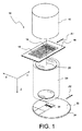
図1は、投影光ビームを生成するための照明システム12を備える投影露光装置10の高度に単純化した斜視図である。投影光ビームは、微細構造18を含むマスク16上の視野14を照明する。この実施形態では、照明視野14は、ほぼリングセグメントの形状を有する。しかしながら、照明視野14の他の形状、例えば矩形も考えられる。
図2は、図1に示す照明システム12のより詳細な子午線断面図である。明確にするために、図2の図は、大幅に簡略化されており一定の縮尺ではない。これは特に、種々の光学ユニットが非常に少数の光学素子によってしか表されていないことを意味する。現実には、これらのユニットは、それよりも大幅に多いレンズ及び他の光学素子を備え得る。
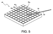
照明システム12は、第1の実施形態によるレーザビーム94を生成する赤外レーザ源92を含む温度制御デバイス90を備え、これはハウジング28内に収容される。温度制御デバイス90は、ミラー素子Mijの標的領域上でレーザビーム94を移動させるように構成される空間光変調器96をさらに含む。この実施形態では、空間光変調器96は、適当なアクチュエータを用いて2つの直交軸に関して傾斜させることができる傾斜可能ミラー98を備える。このような傾斜可能ミラー98は、Microvisionにより出願された国際公開第2005/078506号に記載のようにMEMS技術を用いて実現することもできる。傾斜可能ミラー98を用いて、ミラー98を適宜傾斜させることによりミラーアレイ46の任意の点にレーザビーム94を向けることが可能である。代替的な実施形態では、空間光変調器96は、回転可能なプリズム又は電気光学素子の組み合わせを含み、これは、素子に印加される電圧を変えることにより素子を通過する光ビームの方向を変えることを可能にする。
図8は、別の実施形態によるミラー素子Mijの斜視図である。ミラー素子Mijは、固体関節(solid state articulations)112a、112b、112c、及び112dを用いてキャリア構造110に接続される。これらの関節112a、112b、112c、及び112dは、長手方向スリット113が作られた後でキャリア構造110に残るブリッジにより形成される。簡単のために、対向する関節対112a、112c及び112b、112dによりそれぞれ定められる傾斜軸56x、56yを中心にミラー素子Mijを傾斜させるように構成されるアクチュエータは、図8に示されていない。
本発明の上記の実施形態は、全てDUV照明システムに関する。しかしながら、後述する実施形態から明らかとなるように、本発明は、EUV照明システムでも有利に用いられ得る。このようなシステムでは、投影光の波長(動作波長とも呼ぶ)は、50nm未満、好ましくは25nm未満、最も好ましくは13nm〜14nm未満である。このような短い波長では透明屈折材料が利用不可能であるため、EUV投影露光装置の全光学素子(当然ながら絞り以外)がカトプトリック(すなわち、反射性)タイプである。
Claims (17)
- マイクロリソグラフィ投影露光装置(10)の照明システムであって、
a)一次光源(30)と、
b)システム瞳面(70)と、
c)ミラーアレイ(46)であって、
i)前記一次光源(30)と前記システム瞳面(70)との間に配置され、
ii)複数のアダプティブミラー素子(Mij)を含み、該ミラー素子(Mij)はそれぞれ、
ミラー支持体(100)及び反射性コーティング(102)を含むと共に、
前記一次光源(30)により生成される光(34)を前記システム瞳面(70)に向けるように構成される、
ミラーアレイ(46)と、
を備え、前記ミラー素子(Mij)は、異なる熱膨張係数を有し互いに取り付け固定される構造(100、102)を含み、
該照明システム(12)は、前記ミラー素子(Mij)の形状を個別に変えるために前記構造内の温度分布を可変に変更するように構成される温度制御デバイス(90)を備える、照明システム。
- 前記構造は、前記ミラー支持体(100)及び前記反射性コーティング(102)を含む、請求項1に記載の照明システム。
- 前記構造は、前記反射性コーティング(102)を形成する層を含む、請求項1又は2に記載の照明システム。
- 前記温度制御デバイス(90)は、前記ミラー支持体(100)に取着される加熱部材又は冷却部材(114、114’)を備える、請求項1〜3のいずれか1項に記載の照明システム。
- 前記加熱部材は、導電抵抗線(114’)のパターンを含む、請求項4に記載の照明システム。
- 前記加熱部材又は冷却部材は、ペルチェ素子(130)を含む、請求項4又は5に記載の照明システム。
- 前記温度制御デバイス(90)は、前記ミラー素子(Mij)の前記反射性コーティング(102)の標的領域(106)に放射線を選択的に向けるように構成される放射システムを含む、請求項1〜6のいずれか1項に記載の照明システム。
- 前記反射性コーティング(102)は、前記放射線に対して吸収性がある、請求項7に記載の照明システム。
- 前記放射システムは、放射線ビーム(94)を生成する二次光源(92)と、前記標的領域(106)上で前記放射線ビームを移動させるように構成される空間光変調器(96)とを備える、請求項7又は8に記載の照明システム。
- 前記標的領域(106)は、ミラー素子(Mij)ごとに異なる、請求項7〜9のいずれか1項に記載の照明システム。
- 前記温度制御デバイス(90)は、前記異なる熱膨張係数により生じる屈曲力を考慮に入れることにより前記ミラー素子(Mij)の形状を予測するように構成される、請求項1〜10のいずれか1項に記載の照明システム。
- 前記温度制御デバイス(90)は、前記ミラー素子(Mij)の不均一な温度プロファイルにより生じる屈曲力を考慮に入れることにより前記ミラー素子の形状を予測するように構成される、請求項1〜11のいずれか1項に記載の照明システム。
- 前記ミラー素子(Mij)は、凹面鏡面を有し、前記温度制御デバイス(290)は、前記ミラー素子(Mij)が2つの直交面で異なる焦点距離(fa及びfb)を有するように前記構造内の温度分布を変更するように構成される、請求項1〜12のいずれか1項に記載の照明システム。
- 前記一次光源(230)は、50nm未満の波長を有する投影光を生成するように構成され、前記ミラー素子(Mij)の光軸が、光伝播方向で前記ミラーアレイ(246)の直前にあるミラー(272)の光軸と共に20度よりも大きい角度を形成する、請求項13に記載の照明システム。
- 前記光源(230)に対称軸(AX)が関連付けられ、該対称軸は、水平面に対して45度未満の角度を形成する、請求項14に記載の照明システム。
- 前記ミラー素子(Mij)は、熱障壁(118a、118b)を備え、該熱障壁(118a、118b)は、該熱障壁(118a、118b)の両側に配置される材料(124、100)よりも小さな熱伝導係数を有する、請求項1〜15のいずれか1項に記載の照明システム。
- 各ミラー素子(Mij)が、支持構造に対して傾斜可能に装着される、請求項1〜16のいずれか1項に記載の照明システム。
Applications Claiming Priority (3)
| Application Number | Priority Date | Filing Date | Title |
|---|---|---|---|
| EP08017088A EP2169464A1 (en) | 2008-09-29 | 2008-09-29 | Illumination system of a microlithographic projection exposure apparatus |
| EP08017088.9 | 2008-09-29 | ||
| PCT/EP2009/006856 WO2010034472A1 (en) | 2008-09-29 | 2009-09-23 | Illumination system of a microlithographic projection exposure apparatus |
Publications (3)
| Publication Number | Publication Date |
|---|---|
| JP2012504324A JP2012504324A (ja) | 2012-02-16 |
| JP2012504324A5 JP2012504324A5 (ja) | 2012-11-01 |
| JP5475785B2 true JP5475785B2 (ja) | 2014-04-16 |
Family
ID=40673627
Family Applications (1)
| Application Number | Title | Priority Date | Filing Date |
|---|---|---|---|
| JP2011528238A Active JP5475785B2 (ja) | 2008-09-29 | 2009-09-23 | マイクロリソグラフィ投影露光装置の照明システム |
Country Status (6)
| Country | Link |
|---|---|
| US (2) | US8797507B2 (ja) |
| EP (1) | EP2169464A1 (ja) |
| JP (1) | JP5475785B2 (ja) |
| KR (1) | KR101704069B1 (ja) |
| TW (1) | TWI464542B (ja) |
| WO (1) | WO2010034472A1 (ja) |
Families Citing this family (19)
| Publication number | Priority date | Publication date | Assignee | Title |
|---|---|---|---|---|
| EP2169464A1 (en) | 2008-09-29 | 2010-03-31 | Carl Zeiss SMT AG | Illumination system of a microlithographic projection exposure apparatus |
| DE102010025222A1 (de) * | 2010-06-23 | 2011-12-29 | Carl Zeiss Smt Gmbh | Steuerbare Spiegelanordnung, optisches System mit einer steuerbaren Spiegelanordnung und Verfahren zur Ansteuerung einer steuerbaren Spiegelanordnung |
| WO2012013748A1 (en) * | 2010-07-30 | 2012-02-02 | Carl Zeiss Smt Gmbh | Euv exposure apparatus |
| WO2012034571A1 (en) * | 2010-09-14 | 2012-03-22 | Carl Zeiss Smt Gmbh | Illumination system of a microlithographic projection exposure apparatus |
| DE102010061950A1 (de) * | 2010-11-25 | 2012-05-31 | Carl Zeiss Smt Gmbh | Verfahren sowie Anordnung zum Bestimmen des Erwärmungszustandes eines Spiegels in einem optischen System |
| DE102011005778A1 (de) | 2011-03-18 | 2012-09-20 | Carl Zeiss Smt Gmbh | Optisches Element |
| DE102011005840A1 (de) * | 2011-03-21 | 2012-09-27 | Carl Zeiss Smt Gmbh | Steuerbare Mehrfachspiegelanordnung, optisches System mit einer steuerbaren Mehrfachspiegelanordnung sowie Verfahren zum Betreiben einer steuerbaren Mehrfachspiegelanordnung |
| WO2012169090A1 (ja) * | 2011-06-06 | 2012-12-13 | 株式会社ニコン | 照明方法、照明光学装置、及び露光装置 |
| DE102011104543A1 (de) * | 2011-06-18 | 2012-12-20 | Carl Zeiss Smt Gmbh | Beleuchtungssystem einer mikrolithographischen Projektionsbelichtungsanlage und Verfahren zur mikrolithographischen Projektion einer Maske |
| FR2996016B1 (fr) * | 2012-09-25 | 2014-09-19 | Sagem Defense Securite | Illuminateur de photolithographie telecentrique selon deux directions |
| KR102089310B1 (ko) * | 2013-01-25 | 2020-03-16 | 엘지디스플레이 주식회사 | 마스크리스 노광장치 |
| DE102013204316B4 (de) * | 2013-03-13 | 2015-07-23 | Carl Zeiss Smt Gmbh | Projektionsanordnung |
| US9854226B2 (en) * | 2014-12-22 | 2017-12-26 | Google Inc. | Illuminator for camera system having three dimensional time-of-flight capture with movable mirror element |
| JP6643466B2 (ja) * | 2015-09-23 | 2020-02-12 | カール・ツァイス・エスエムティー・ゲーエムベーハー | マイクロリソグラフィ投影装置を動作させる方法およびそのような装置の照明システム |
| CN110520799B (zh) * | 2017-04-12 | 2022-06-10 | Asml荷兰有限公司 | 反射镜阵列 |
| DE102017221420A1 (de) | 2017-11-29 | 2018-11-29 | Carl Zeiss Smt Gmbh | Euv-beleuchtungssystem und verfahren zum erzeugen einer beleuchtungsstrahlung |
| DE102018123328B4 (de) * | 2018-09-21 | 2022-09-08 | Carl Zeiss Smt Gmbh | Baugruppe eines optischen Systems, insbesondere in einer mikrolithographischen Projektionsbelichtungsanlage, sowie Verfahren zum Betreiben eines solchen optischen Systems |
| KR20200043767A (ko) * | 2018-10-18 | 2020-04-28 | 삼성전자주식회사 | Euv 노광 장치와 노광 방법, 및 그 노광 방법을 포함한 반도체 소자 제조 방법 |
| EP4261580A1 (en) * | 2022-04-14 | 2023-10-18 | Airbus Defence and Space GmbH | Apparatus and method for altering an optical surface of a mirror |
Family Cites Families (26)
| Publication number | Priority date | Publication date | Assignee | Title |
|---|---|---|---|---|
| CA2077572C (en) | 1991-09-07 | 1998-08-18 | Masahito Niibe | Method of and apparatus for stabilizing shapes of objects, such as optical elements, as well as exposure apparatus using same and method of manufacturing semiconductr devices |
| DE10140208C2 (de) | 2001-08-16 | 2003-11-06 | Zeiss Carl | Optische Anordnung |
| JP4320999B2 (ja) * | 2002-02-04 | 2009-08-26 | 株式会社ニコン | X線発生装置及び露光装置 |
| JP4324957B2 (ja) | 2002-05-27 | 2009-09-02 | 株式会社ニコン | 照明光学装置、露光装置および露光方法 |
| WO2004034447A1 (ja) * | 2002-10-10 | 2004-04-22 | Nikon Corporation | 極短紫外線光学系用反射ミラー、極短紫外線光学系、極短紫外線光学系の使用方法、極短紫外線光学系の製造方法、極短紫外線露光装置、及び極短紫外線露光装置の使用方法 |
| US6996343B2 (en) * | 2003-03-21 | 2006-02-07 | Lucent Technologies Inc. | Dispersion compensator |
| DE10317662A1 (de) | 2003-04-17 | 2004-11-18 | Carl Zeiss Smt Ag | Projektionsobjektiv, mikrolithographische Projektionsbelichtungsanlage und Verfahren zur Herstellung einer Halbleiterschaltung |
| DE10327733C5 (de) | 2003-06-18 | 2012-04-19 | Limo Patentverwaltung Gmbh & Co. Kg | Vorrichtung zur Formung eines Lichtstrahls |
| TWI220097B (en) * | 2003-07-21 | 2004-08-01 | Avision Inc | Image calibration method |
| JP4717813B2 (ja) * | 2003-09-12 | 2011-07-06 | カール・ツァイス・エスエムティー・ゲーエムベーハー | マイクロリソグラフィ投影露光設備のための照明系 |
| US20050280879A1 (en) | 2004-02-09 | 2005-12-22 | Gibson Gregory T | Method and apparatus for scanning a beam of light |
| KR101170182B1 (ko) | 2004-02-17 | 2012-08-01 | 칼 짜이스 에스엠티 게엠베하 | 마이크로 리소그래피 투영 노광 장치용 조명 시스템 |
| WO2005083512A2 (de) * | 2004-02-26 | 2005-09-09 | Carl Zeiss Smt Ag | Beleuchtungssystem für eine mikrolithographie-projektionsbelichtungsanlage |
| US7079225B2 (en) * | 2004-09-14 | 2006-07-18 | Asml Netherlands B.V | Lithographic apparatus and device manufacturing method |
| US20100014063A1 (en) * | 2005-05-31 | 2010-01-21 | Fujifilm Corporation | Image exposure apparatus |
| JP2007150295A (ja) * | 2005-11-10 | 2007-06-14 | Carl Zeiss Smt Ag | ラスタ要素を有する光学装置、及びこの光学装置を有する照射システム |
| JP4778834B2 (ja) * | 2006-05-24 | 2011-09-21 | 富士フイルム株式会社 | 画像記録方法及び装置 |
| US8052289B2 (en) * | 2006-06-07 | 2011-11-08 | Asml Netherlands B.V. | Mirror array for lithography |
| EP1890191A1 (en) * | 2006-08-14 | 2008-02-20 | Carl Zeiss SMT AG | Catadioptric projection objective with pupil mirror |
| DE102006039895A1 (de) * | 2006-08-25 | 2008-03-13 | Carl Zeiss Smt Ag | Verfahren zur Korrektur von durch Intensitätsverteilungen in optischen Systemen erzeugten Abbildungsveränderungen sowie entsprechendes optisches System |
| US7804603B2 (en) * | 2006-10-03 | 2010-09-28 | Asml Netherlands B.V. | Measurement apparatus and method |
| JP5098306B2 (ja) * | 2006-11-22 | 2012-12-12 | 株式会社ニコン | 露光装置、デバイス製造方法、及び露光方法 |
| DE102008002377A1 (de) * | 2007-07-17 | 2009-01-22 | Carl Zeiss Smt Ag | Beleuchtungssystem sowie Projektionsbelichtungsanlage für die Mikrolithografie mit einem derartigen Beleuchtungssystem |
| JP5579063B2 (ja) * | 2007-08-24 | 2014-08-27 | カール・ツァイス・エスエムティー・ゲーエムベーハー | 制御可能な光学素子、熱アクチュエータによる光学素子の操作方法および半導体リソグラフィのための投影露光装置 |
| TWI531872B (zh) * | 2008-09-22 | 2016-05-01 | Asml荷蘭公司 | 微影裝置、可程式化圖案化器件及微影方法 |
| EP2169464A1 (en) * | 2008-09-29 | 2010-03-31 | Carl Zeiss SMT AG | Illumination system of a microlithographic projection exposure apparatus |
-
2008
- 2008-09-29 EP EP08017088A patent/EP2169464A1/en not_active Withdrawn
-
2009
- 2009-09-23 WO PCT/EP2009/006856 patent/WO2010034472A1/en active Application Filing
- 2009-09-23 KR KR1020117009693A patent/KR101704069B1/ko active IP Right Grant
- 2009-09-23 JP JP2011528238A patent/JP5475785B2/ja active Active
- 2009-09-25 TW TW098132466A patent/TWI464542B/zh active
-
2011
- 2011-03-09 US US13/044,160 patent/US8797507B2/en active Active
-
2014
- 2014-06-25 US US14/314,725 patent/US9523922B2/en active Active
Also Published As
| Publication number | Publication date |
|---|---|
| US20110181850A1 (en) | 2011-07-28 |
| TW201022854A (en) | 2010-06-16 |
| KR20110059800A (ko) | 2011-06-03 |
| TWI464542B (zh) | 2014-12-11 |
| WO2010034472A1 (en) | 2010-04-01 |
| JP2012504324A (ja) | 2012-02-16 |
| US20140307239A1 (en) | 2014-10-16 |
| EP2169464A1 (en) | 2010-03-31 |
| US8797507B2 (en) | 2014-08-05 |
| US9523922B2 (en) | 2016-12-20 |
| KR101704069B1 (ko) | 2017-02-07 |
Similar Documents
| Publication | Publication Date | Title |
|---|---|---|
| JP5475785B2 (ja) | マイクロリソグラフィ投影露光装置の照明システム | |
| US10191382B2 (en) | Illumination system for illuminating a mask in a microlithographic exposure apparatus | |
| JP5337304B2 (ja) | マイクロリソグラフィ投影露光装置及びそこに収容される光学面に関連するパラメータを測定する方法 | |
| JP5727005B2 (ja) | 光学系及びマルチファセットミラー | |
| JP5863974B2 (ja) | マイクロリソグラフィ投影露光装置の投影対物レンズ | |
| JP5587917B2 (ja) | マイクロリソグラフィ投影露光装置 | |
| JP6186623B2 (ja) | マイクロリソグラフィ投影露光装置 | |
| US20130293861A1 (en) | Illumination system of a microlithographic projection exposure apparatus | |
| US8724080B2 (en) | Optical raster element, optical integrator and illumination system of a microlithographic projection exposure apparatus | |
| WO2012034571A1 (en) | Illumination system of a microlithographic projection exposure apparatus | |
| JP2017526969A (ja) | Euv投影リソグラフィのための照明光学ユニット | |
| US9261695B2 (en) | Illumination system of a microlithographic projection exposure apparatus |
Legal Events
| Date | Code | Title | Description |
|---|---|---|---|
| A521 | Request for written amendment filed |
Free format text: JAPANESE INTERMEDIATE CODE: A523 Effective date: 20120911 |
|
| A621 | Written request for application examination |
Free format text: JAPANESE INTERMEDIATE CODE: A621 Effective date: 20120911 |
|
| A977 | Report on retrieval |
Free format text: JAPANESE INTERMEDIATE CODE: A971007 Effective date: 20130911 |
|
| A131 | Notification of reasons for refusal |
Free format text: JAPANESE INTERMEDIATE CODE: A131 Effective date: 20130917 |
|
| A521 | Request for written amendment filed |
Free format text: JAPANESE INTERMEDIATE CODE: A523 Effective date: 20131216 |
|
| TRDD | Decision of grant or rejection written | ||
| A01 | Written decision to grant a patent or to grant a registration (utility model) |
Free format text: JAPANESE INTERMEDIATE CODE: A01 Effective date: 20140114 |
|
| A61 | First payment of annual fees (during grant procedure) |
Free format text: JAPANESE INTERMEDIATE CODE: A61 Effective date: 20140206 |
|
| R150 | Certificate of patent or registration of utility model |
Ref document number: 5475785 Country of ref document: JP Free format text: JAPANESE INTERMEDIATE CODE: R150 Free format text: JAPANESE INTERMEDIATE CODE: R150 |
|
| R250 | Receipt of annual fees |
Free format text: JAPANESE INTERMEDIATE CODE: R250 |
|
| R250 | Receipt of annual fees |
Free format text: JAPANESE INTERMEDIATE CODE: R250 |
|
| R250 | Receipt of annual fees |
Free format text: JAPANESE INTERMEDIATE CODE: R250 |
|
| R250 | Receipt of annual fees |
Free format text: JAPANESE INTERMEDIATE CODE: R250 |
|
| R250 | Receipt of annual fees |
Free format text: JAPANESE INTERMEDIATE CODE: R250 |
|
| R250 | Receipt of annual fees |
Free format text: JAPANESE INTERMEDIATE CODE: R250 |
|
| R250 | Receipt of annual fees |
Free format text: JAPANESE INTERMEDIATE CODE: R250 |
|
| R250 | Receipt of annual fees |
Free format text: JAPANESE INTERMEDIATE CODE: R250 |