JP5452155B2 - Surge voltage suppression device and motor control device - Google Patents
Surge voltage suppression device and motor control device Download PDFInfo
- Publication number
- JP5452155B2 JP5452155B2 JP2009232454A JP2009232454A JP5452155B2 JP 5452155 B2 JP5452155 B2 JP 5452155B2 JP 2009232454 A JP2009232454 A JP 2009232454A JP 2009232454 A JP2009232454 A JP 2009232454A JP 5452155 B2 JP5452155 B2 JP 5452155B2
- Authority
- JP
- Japan
- Prior art keywords
- surge voltage
- voltage
- unit
- voltage suppression
- terminal
- Prior art date
- Legal status (The legal status is an assumption and is not a legal conclusion. Google has not performed a legal analysis and makes no representation as to the accuracy of the status listed.)
- Expired - Fee Related
Links
Images


Description
本発明は、インバータによりモータが駆動される際に、そのモータ端にて発生するサージ電圧を抑制するサージ電圧抑制装置およびこのサージ電圧抑制装置を備えたモータ制御装置に関する。 The present invention relates to a surge voltage suppression device that suppresses a surge voltage generated at the motor end when a motor is driven by an inverter, and a motor control device including the surge voltage suppression device.
電圧形PWM方式のインバータは、矩形波状(パルス状)の電圧を出力する。このような出力電圧は、電圧変化率(dV/dt)が高いため、非常に高い周波数成分を含んでいる。また、インバータの出力電圧は、ケーブルを介してモータに供給される。このようなことから、ケーブルとモータのインピーダンスの相違による反射共振などが原因で、モータ端においてサージ電圧が発生する。このサージ電圧は、上記ケーブルの長さや種類(インピーダンス)、布設方法などに依存しており、その最大値はインバータの出力端における電圧の2倍以上になることが知られている。上記サージ電圧が原因で、モータの巻線のうち、特にインバータに近い側の巻線部分の絶縁が劣化してしまう。モータ巻線の絶縁劣化が進むと、最悪の場合には絶縁破壊に至る可能性もあり、その場合には非常に危険な状態となる。 The voltage-type PWM inverter outputs a rectangular wave (pulse) voltage. Since such an output voltage has a high voltage change rate (dV / dt), it includes a very high frequency component. The output voltage of the inverter is supplied to the motor via a cable. For this reason, a surge voltage is generated at the motor end due to reflection resonance due to the difference in impedance between the cable and the motor. This surge voltage depends on the length and type (impedance) of the cable, the laying method, etc., and the maximum value is known to be twice or more the voltage at the output terminal of the inverter. Due to the surge voltage, the insulation of the winding portion of the motor winding, particularly on the side close to the inverter, is deteriorated. If the insulation deterioration of the motor winding proceeds, there is a possibility that the insulation breakdown may occur in the worst case, and in this case, a very dangerous state is caused.
そこで、インバータ出力端またはモータ端に、交流リアクトル、サージ電圧抑制フィルタなどを付加し、サージ電圧の発生を抑制することが広く行われている。ただし、一般にこれらの付加装置は価格が高い上、大きく且つ重い。このため、その設置に多大な労力を要するとともに設置スペースを広くとらなければならない。
一方、特許文献1には、サージ吸収用の半導体素子を用いてサージ電圧を抑制する技術が開示されている。このものによれば、所定の電圧を超えるサージ電圧が印加されると、半導体素子が電流を流し、その電圧を所定値にクランプする。このような動作によってサージ電圧が抑制される。
Therefore, it is widely practiced to suppress the generation of a surge voltage by adding an AC reactor, a surge voltage suppression filter or the like to the inverter output terminal or the motor terminal. However, these additional devices are generally expensive and large and heavy. For this reason, the installation requires a great deal of labor and a large installation space.
On the other hand, Patent Document 1 discloses a technique for suppressing a surge voltage by using a semiconductor element for surge absorption. According to this device, when a surge voltage exceeding a predetermined voltage is applied, the semiconductor element passes a current and clamps the voltage to a predetermined value. Such an operation suppresses the surge voltage.
一般的に使用されるサージ吸収用の半導体素子としては、例えばツェナーダイオードが挙げられる。現状、ツェナーダイオードの定格電圧(ツェナー電圧の定格値)は、最大でも400V程度である。一方、モータに生じるサージ電圧の電圧値は、少なくとも1000V程度となる。このことから、特許文献1記載の半導体素子を、前述したインバータにより駆動されるモータ端の例えば各相間に接続してサージ電圧を抑制しようとする場合、次のような問題が生じる。 As a semiconductor element for surge absorption generally used, for example, a Zener diode can be cited. At present, the rated voltage of the Zener diode (rated value of the Zener voltage) is about 400 V at the maximum. On the other hand, the voltage value of the surge voltage generated in the motor is at least about 1000V. For this reason, when the semiconductor element described in Patent Document 1 is connected between, for example, each phase of the motor end driven by the above-described inverter, the following problem arises.
すなわち、モータ端に生じるサージ電圧を抑制するためには、各相間に複数の上記半導体素子を直列に接続することで単体でのクランプ電圧よりも高いクランプ電圧を実現する必要がある。しかし、このように複数の半導体素子を直列接続して用いると、各素子の特性のばらつきに起因して各半導体素子が分担する電圧が不平等になってしまう。分担電圧が不平等になると、高い電圧を分担している素子が故障してしまう可能性が生じる。 That is, in order to suppress the surge voltage generated at the motor end, it is necessary to realize a clamp voltage higher than the single clamp voltage by connecting a plurality of the semiconductor elements in series between the phases. However, when a plurality of semiconductor elements are connected in series as described above, the voltage shared by each semiconductor element becomes unequal due to variations in the characteristics of each element. If the shared voltage becomes unequal, there is a possibility that an element sharing a high voltage will fail.
半導体素子の故障には、大きく分けて短絡モードと開放モードとがあるが、開放モードで故障する場合でも、まず短絡故障が発生し、それに伴い流れる過大な電流により素子内部の最も弱い部分が溶断して最終的に開放モードになる。つまり、半導体素子が故障する際、必ず最初に短絡状態が生じる。このことから、直列接続された半導体素子の1つが故障すると、その半導体素子は必ず短絡状態となる。そして、この故障した半導体素子が分担していた電圧が残りの半導体素子に印加されることで、これらが連鎖的に故障するおそれがある。全ての半導体素子が故障状態になると、モータの各相間が短絡状態になる。 Semiconductor device failures can be broadly divided into short-circuit mode and open-mode. Even when a failure occurs in open-mode, a short-circuit failure occurs first, and the weakest part inside the device is blown out by excessive current that flows. Finally, it becomes the release mode. That is, when a semiconductor element fails, a short circuit state always occurs first. From this, when one of the semiconductor elements connected in series fails, the semiconductor element is always short-circuited. Then, when the voltage shared by the failed semiconductor element is applied to the remaining semiconductor elements, they may fail in a chained manner. When all the semiconductor elements are in a failure state, the motor phases are short-circuited.
通常、モータの各相間が短絡状態になると、インバータ側において、出力電流の過電流保護機能が動作してインバータ出力が遮断されるようになっている。しかし、この保護機能が動作する前に、故障した半導体素子が開放モードに移行した場合、モータの短絡状態が解消される。このようになると、半導体素子の故障によりサージ電圧抑制のための機能が無効化しているにもかかわらず、それに気付かずに運転が継続されてしまい、前述したサージ電圧による問題が生じるおそれがある。一方、上記保護機能が動作してインバータ出力が遮断された場合であっても、遮断される前の一時的な短絡状態において過大な電流が流れ、主系統の他の機器に悪影響を及ぼす可能性がある。 Normally, when each phase of the motor is short-circuited, an output current overcurrent protection function is operated on the inverter side to shut off the inverter output. However, if the failed semiconductor element enters the open mode before this protection function operates, the short circuit state of the motor is eliminated. In this case, although the function for suppressing the surge voltage is invalidated due to the failure of the semiconductor element, the operation is continued without noticing it, and there is a possibility that the above-described problem due to the surge voltage occurs. On the other hand, even when the above protective function is activated and the inverter output is shut off, excessive current may flow in the temporary short circuit state before the shutoff, possibly adversely affecting other devices in the main system There is.
そこで、このような半導体素子の故障を検出するための構成を付加することが考えられる。例えば、特許文献2には、サージ電圧吸収用の半導体素子と直列に発光ダイオードまたはフォトカプラの発光素子を接続し、半導体素子が完全な短絡状態となる前の低インピーダンス状態を発光ダイオードの発光状態またはフォトカプラの受光素子の駆動状態により検出する技術が開示されている。
Therefore, it is conceivable to add a configuration for detecting such a failure of the semiconductor element. For example, in
この特許文献2の技術を用いて、上記モータの各相間に接続したサージ吸収用の半導体素子の故障を検出しようとすると、以下のような問題が生じる。すなわち、素子が上述した低インピーダンス状態である期間は長いとは限らない。従って、この低インピーダンス状態を検出して何らかの保護動作を実行する前に、半導体素子が完全な短絡状態になる可能性がある。このようになると、短絡電流が流れることにより半導体素子および発光ダイオードなどの検出素子も故障する可能性があり、有効な故障検出ができないことになる。
If it is attempted to detect a failure of the semiconductor element for surge absorption connected between the phases of the motor using the technique of
本発明は上記事情に鑑みてなされたものであり、その目的は、サージ電圧を抑制するために用いる半導体素子の特性のばらつきに起因した故障を防ぐとともに、半導体素子の故障状態を直ちに検出することができるサージ電圧抑制装置およびこのサージ電圧抑制装置を備えたモータ制御装置を提供することにある。 The present invention has been made in view of the above circumstances, and an object of the present invention is to prevent a failure caused by variations in characteristics of a semiconductor element used for suppressing a surge voltage and to immediately detect a failure state of the semiconductor element. The present invention is to provide a surge voltage suppressing device capable of performing the above and a motor control device including the surge voltage suppressing device.
上記した目的を達成するために、本発明のサージ電圧抑制装置は、電圧形PWM方式のインバータによりモータが駆動される際に、そのモータ端にて発生するサージ電圧を抑制するサージ電圧抑制装置であって、前記モータ端の各相に対応して設けられ、当該各相の電圧が所定のクランプ電圧を超えて上昇しようとすると当該モータ端から電流を流すことで、当該各相の電圧を前記クランプ電圧に制限するクランプ部と、前記クランプ部に対応して設けられ、対応する前記クランプ部が短絡故障すると、直ちに当該クランプ部が介在する通電経路を遮断する保護動作を行う保護部と、前記保護部に対応して設けられ、対応する前記保護部により前記保護動作が行われたことを検出すると、その保護部に対応する前記クランプ部が故障状態であることを表す故障検出信号を外部に出力する故障検出部とを備え、前記クランプ部は、ドレイン・ソース間に内蔵されたボディダイオードを有する第1および第2のパワーMOSFETを備え、前記第1および第2のパワーMOSFETのゲート・ソース間をそれぞれ短絡するとともに、前記第1のパワーMOSFETと前記第2のパワーMOSFETとを前記ボディダイオードによる整流方向が互いに逆向きとなるように直列に接続して構成されていることを特徴とする。 In order to achieve the above object, the surge voltage suppression device of the present invention is a surge voltage suppression device that suppresses a surge voltage generated at the motor end when the motor is driven by a voltage-type PWM inverter. The voltage of each phase is provided corresponding to each phase of the motor end, and when the voltage of the phase exceeds the predetermined clamp voltage, current flows from the motor end, A clamping unit that limits to a clamping voltage, a protection unit that is provided corresponding to the clamping unit, and that performs a protective operation that immediately shuts off an energization path interposed by the clamping unit when the corresponding clamping unit is short-circuited; When it is detected that the protection operation has been performed by the corresponding protection unit, the clamp unit corresponding to the protection unit is in a failure state. A failure detection unit that outputs a failure detection signal representing the above to the outside, wherein the clamp unit includes first and second power MOSFETs having a body diode built in between a drain and a source, The gate and the source of the second power MOSFET are short-circuited, and the first power MOSFET and the second power MOSFET are connected in series so that the rectification directions by the body diodes are opposite to each other. It is configured.
上記構成によれば、従来はサージ吸収用途に用いられることがなかったパワーMOSFETによりクランプ部が構成されている。なお、このパワーMOSFETは、ドレイン・ソース間の耐圧実力値の高いものまで広く流通しており、所定のクランプ電圧に合わせて耐圧実力値を選定することが可能である。そして、第1および第2のパワーMOSFETは、各相の電圧の極性に応じていずれか一方のみがアバランシェ動作し、そのドレイン・ソース間電圧は耐圧実力値に制限され、これにより、モータ端におけるサージ電圧が所定のクランプ値に制限される。 According to the said structure, the clamp part is comprised with power MOSFET which was not used for the surge absorption use conventionally. The power MOSFETs are widely distributed up to those having a high withstand voltage value between the drain and the source, and the withstand voltage value can be selected according to a predetermined clamp voltage. Only one of the first and second power MOSFETs is avalanche-operated according to the polarity of the voltage of each phase, and the drain-source voltage is limited to the withstand voltage capability value. The surge voltage is limited to a predetermined clamp value.
本発明によれば、クランプ部を構成する第1および第2のパワーMOSFETは、各相の電圧の極性に応じていずれか一方のみがクランプ動作を行うので、各半導体素子の特性のばらつきに起因する故障が発生することはない。また、保護部による保護動作が行われたことを検出すると、その保護部に対応するクランプ部が故障状態であることを表す故障検出信号を外部に出力する検出部を備えているので、サージ電圧を抑制することができない状態で、インバータの運転が継続されることを確実に防止することができる。 According to the present invention, only one of the first and second power MOSFETs constituting the clamp unit performs the clamping operation according to the polarity of the voltage of each phase, which is caused by variations in characteristics of each semiconductor element. There will be no failure to occur. In addition, since it has a detection unit that outputs a failure detection signal indicating that the clamp unit corresponding to the protection unit is in a failure state when it detects that the protection operation by the protection unit has been performed, the surge voltage It is possible to reliably prevent the operation of the inverter from being continued in a state where it cannot be suppressed.
(第1の実施形態)
以下、本発明の第1の実施形態について図1〜図3を参照しながら説明する。
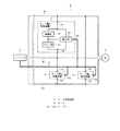
図1は、モータ制御装置の電気構成を概略的に示している。図1に示すモータ制御装置1は、汎用の電圧形インバータ2によりモータ3をPWM駆動して制御するものである。インバータ2の各出力端子には、電圧供給線4u、4v、4w(ケーブルに相当)を介してモータ3の各相端子が接続されている。モータ3は、例えば三相の交流モータである。
(First embodiment)
Hereinafter, a first embodiment of the present invention will be described with reference to FIGS.
FIG. 1 schematically shows the electrical configuration of the motor control device. A motor control device 1 shown in FIG. 1 controls a
インバータ2は、直流電源回路(図示せず)、インバータ主回路、ゲート駆動回路(図3に符号5を付して示す)、制御部(図3に符号6を付して示す)などから構成されている。直流電源回路は、交流電源より供給される交流を整流および平滑して出力する。インバータ主回路は、スイッチング素子を三相フルブリッジ接続して構成されたものであり、直流電源回路から出力される直流電圧を三相交流電圧に変換する。この三相交流電圧は、インバータ2の負荷であるモータ3に供給される。制御部6は、インバータ主回路からパルス幅変調された指定周波数の三相交流電圧が出力されるようにインバータ主回路の各スイッチング素子の駆動をゲート駆動回路5を介して制御する。
The
電圧供給線4u−4v間、電圧供給線4v−4w間および電圧供給線4u−4w間には、それぞれサージ電圧抑制装置7、8および9が接続されている。サージ電圧抑制装置7〜9は、モータ3端において発生するサージ電圧を抑制するものであり、クランプ部10、保護部11、検出部12および端子P1〜P3を備えている。
Surge
クランプ部10は、端子P1、P2間の電圧を所定のクランプ電圧VCPに制限する。保護部11は、クランプ部10が短絡故障した場合に、端子P1、P2間の通電経路を遮断する保護動作を行う。検出部12は、保護部11による保護動作が行われたことを検出するものであり、その保護動作を検出すると、クランプ部10が故障状態であることを表す故障検出信号を端子P3を介してインバータ2に出力する。なお、インバータ2と検出部12との間には、実際には複数の信号線が接続されるが、図1では、これら複数の信号線を1つの複合信号線13(多芯線ケーブル)として表している。
The
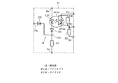
図2は、サージ電圧抑制装置の具体的な構成を示している。なお、図2には、サージ電圧抑制装置7の構成のみを示すが、サージ電圧抑制装置8、9についても同様に構成されている。クランプ部10は、トランジスタM1、M2を備えている。トランジスタM1、M2は、Nチャネル型のパワーMOSFETであり、それぞれドレイン・ソース間に接続されたボディダイオードBD1、BD2を備えている。トランジスタM1、M2は、ドレイン・ソース間の耐圧実力値(実力耐圧)が1000V程度のものを選定して使用している。これにより、詳細の動作は後述するが、クランプ部10のクランプ電圧VCPは、約1000Vとなっている。
FIG. 2 shows a specific configuration of the surge voltage suppressor. FIG. 2 shows only the configuration of the surge
トランジスタM1、M2は、いずれもゲート・ソース間が短絡されており、通常はオフ状態に固定されている。トランジスタM1、M2は、各ソースが互いに接続されている。トランジスタM1のドレインはノードNaに接続され、トランジスタM2のドレインはノードNbに接続されている。 In each of the transistors M1 and M2, the gate and the source are short-circuited and are normally fixed in an off state. The sources of the transistors M1 and M2 are connected to each other. The drain of the transistor M1 is connected to the node Na, and the drain of the transistor M2 is connected to the node Nb.
保護部11は、速断型のヒューズF1を備えている。ヒューズF1の両端子は、それぞれノードNc、Ndに接続されている。保護部11とクランプ部10とは、端子P1と端子P2の間に直列に接続されている。すなわち、端子P1とノードNcが接続され、ノードNdとノードNaが接続され、ノードNbが端子P2に接続されている。
The
検出部12は、フォトカプラPC1、ダイオードD1、D2および抵抗R1、R2を備えている。ノードNeとノードNfの間には、フォトカプラPC1の一次側発光素子である発光ダイオードLD1、ダイオードD1および抵抗R1が直列に接続されている。また、ノードNgとノードNfの間には、ダイオードD2および抵抗R1が直列に接続されている。ノードNeは端子P1に接続され、ノードNfは端子P2に接続され、ノードNgは、クランプ部10のノードNaと保護部11のノードNdと共通に接続されている。抵抗R1は、端子P1と端子P2の間の通電経路に流れる電流を制限するものであり、高抵抗値のものが使用される。ダイオードD2は、ダイオードD1と抵抗R1の相互接続点Nhの電位を、ヒューズF1が導通している状態且つ後述する特定の条件下において、端子P1の電圧からダイオードD2の順方向電圧VFを減じた電圧に固定するために設けられている。
The
フォトカプラPC1は、トランジスタ出力型のものであり、その二次側受光素子は、フォトダイオードPD1およびNPN形のトランジスタT1を集積化して構成されている。フォトダイオードPD1のカソードとトランジスタT1のコレクタとは共通に接続されるとともにノードNiに接続されている。トランジスタT1のエミッタは、ノードNjに接続されるとともに、抵抗R2を介してノードNkに接続されている。抵抗R2は、トランジスタT1のコレクタ電流を制限するとともに、トランジスタT1がオフしている期間にノードNjの電位をノードNkの電位に固定するプルダウン抵抗である。ノードNi、Nkは、それぞれ端子Vcc、端子Nに接続されている。サージ電圧抑制装置7は、インバータ2から端子Vcc、Nを介して直流電圧Vccの供給を受けるようになっている。ノードNjは、故障検出信号の出力端子である端子Voに接続されている。これら端子Vcc、Vo、Nは、図1における端子P3に相当する。
The photocoupler PC1 is of a transistor output type, and its secondary side light receiving element is configured by integrating a photodiode PD1 and an NPN transistor T1. The cathode of the photodiode PD1 and the collector of the transistor T1 are connected in common and connected to the node Ni. The emitter of the transistor T1 is connected to the node Nj and is connected to the node Nk via the resistor R2. The resistor R2 is a pull-down resistor that limits the collector current of the transistor T1 and fixes the potential of the node Nj to the potential of the node Nk while the transistor T1 is off. Nodes Ni and Nk are connected to terminal Vcc and terminal N, respectively. The surge
本実施形態では、トランジスタT1がオンして端子Voの電圧が端子Vccの電圧(直流電圧Vcc=Hレベル)と等しくなる状態が故障検出信号が出力された状態に相当する。また、トランジスタT1がオフして端子Voの電圧が端子Nの電圧(接地電位=Lレベル)と等しくなる状態が故障検出信号が出力されない状態に相当する。また、本実施形態では、ダイオードD1、D2および抵抗R1により検出電流供給部14が構成されている。
In this embodiment, the state in which the transistor T1 is turned on and the voltage at the terminal Vo becomes equal to the voltage at the terminal Vcc (DC voltage Vcc = H level) corresponds to the state in which the failure detection signal is output. A state in which the transistor T1 is turned off and the voltage at the terminal Vo becomes equal to the voltage at the terminal N (ground potential = L level) corresponds to a state in which no failure detection signal is output. In the present embodiment, the detection
図3は、モータ制御装置におけるクランプ部の故障検出に係る部分の構成を示している。サージ電圧抑制装置7〜9の端子Vccは、いずれもインバータ2の内部において、直流電圧Vccの供給端子に接続されている。サージ電圧抑制装置7〜9の端子Nは、いずれもインバータ2の内部において、接地電位(基準電位)の供給端子に接続されている。サージ電圧抑制装置7〜9の端子Voは、いずれもインバータ2の内部において、制御部6に接続されている。このような構成により、インバータ2からサージ電圧抑制装置7〜9に対し、接地電位を基準とした直流電圧Vccが供給される。また、サージ電圧抑制装置7〜9のそれぞれの端子Voの電圧がインバータ2の制御部6に入力される。
FIG. 3 shows a configuration of a portion related to failure detection of the clamp portion in the motor control device. The terminals Vcc of the surge
制御部6は、例えばCPU、ROM、RAMなどを備えたマイクロコンピュータを主体として構成されている。また、制御部6は、ソフトウエアにより構成されたラッチ回路を備えている。制御部6は、このラッチ回路を用いて入力される各端子Voの電圧の立ち上がりを検出する。制御部6は、端子Voの電圧の立ち上がりを所定回数だけ検出すると、それに対応するサージ電圧抑制装置から故障検出信号が与えられたと判断し、所定の故障対応制御を実行する。この故障対応制御としては、例えば、ゲート駆動回路5を介してインバータ2の出力を遮断する制御や、表示部15を介してサージ電圧抑制装置7〜9が故障である旨を表示する制御などがある。
The
次に、上記構成のサージ電圧抑制装置の動作について説明する。
以下では、電圧供給線4u−4v間に接続されたサージ電圧抑制装置7の動作を例にして説明を行うが、サージ電圧抑制装置8、9についても同様の動作となる。なお、以下では、端子P1の電圧をVP1とし、端子P2の電圧をVP2として表す。まず、トランジスタM1、M2がいずれも故障していない状態の動作について説明する。
Next, the operation of the surge voltage suppressor having the above configuration will be described.
Hereinafter, the operation of the surge
(1)「クランプ電圧VCP>電圧VP1−電圧VP2>0」であるときの動作
この場合には、モータ3端においてクランプ電圧VCPを超えるサージ電圧が発生していない。このとき、トランジスタM1、M2はいずれも通常のオフ状態である。このため、端子P1、ヒューズF1、ダイオードD2、抵抗R1、端子P2という経路で電流が流れる。なお、ノードNhの電位が、「電圧VP1−順方向電圧VF」に固定されるので、フォトカプラPC1の発光ダイオードLD1には電流は流れない。このため、トランジスタT1はオフとなり、端子Voの電圧はLレベルとなる。
(1) Operation when “Clamp Voltage VCP> Voltage VP1−Voltage VP2> 0” In this case, no surge voltage exceeding the clamp voltage VCP is generated at the
(2)「クランプ電圧VCP>電圧VP2−電圧VP1>0」であるときの動作
この場合にも、モータ3端においてクランプ電圧VCPを超えるサージ電圧が発生していない。このとき、トランジスタM1、M2はいずれも通常のオフ状態である。ただし、この場合、ダイオードD1、D2の逆流阻止作用(整流作用)により、端子P1、P2間には電流は流れない。従って、トランジスタT1はオフとなり、端子Voの電圧はLレベルとなる。
(2) Operation when “Clamp Voltage VCP> Voltage VP2−Voltage VP1> 0” Also in this case, no surge voltage exceeding the clamp voltage VCP is generated at the
(3)「電圧VP1−電圧VP2>クランプ電圧VCP」であるときの動作
端子P2の電位を基準とした端子P1、P2間の電圧がクランプ電圧VCPを超えて上昇しようとすると、トランジスタM1がアバランシェ動作を行う。すなわち、ゲート・ソース間が短絡されたトランジスタM1のドレイン・ソース間に電流が流れ、そのドレイン・ソース間電圧が耐圧実力値(=クランプ電圧VCP)で安定する。この際、トランジスタM1のドレイン電流は、ボディダイオードBD2を通じて端子P2へと流れる。このような動作により、端子P1、P2間の電圧、つまり、電圧供給線4u、4v間の電圧は、約1000Vのクランプ電圧VCPに制限される。この際にも、トランジスタT1はオフであり、端子Voの電圧はLレベルとなる。
(3) Operation when “Voltage VP1−Voltage VP2> Clamping Voltage VCP” When the voltage between the terminals P1 and P2 with respect to the potential of the terminal P2 is to exceed the clamp voltage VCP, the transistor M1 is avalanche. Perform the action. That is, a current flows between the drain and source of the transistor M1 whose gate and source are short-circuited, and the drain-source voltage is stabilized at the withstand voltage capability value (= clamp voltage VCP). At this time, the drain current of the transistor M1 flows to the terminal P2 through the body diode BD2. By such an operation, the voltage between the terminals P1 and P2, that is, the voltage between the
(4)「電圧VP2−電圧VP1>クランプ電圧VCP」であるときの動作
端子P1の電位を基準とした端子P2、P1間の電圧がクランプ電圧VCPを超えて上昇しようとすると、トランジスタM2がアバランシェ動作を行う。すなわち、ゲート・ソース間が短絡されたトランジスタM2のドレイン・ソース間に電流が流れ、そのドレイン・ソース間電圧が耐圧実力値(=クランプ電圧VCP)で安定する。この際、トランジスタM2のドレイン電流は、ボディダイオードBD1を通じて端子P1へと流れる。このような動作により、端子P2、P1間の電圧、つまり電圧供給線4v、4u間の電圧は、約1000Vのクランプ電圧VCPに制限される。この際にも、トランジスタT1はオフであり、端子Voの電圧はLレベルとなる。
(4) Operation when “Voltage VP2−Voltage VP1> Clamping Voltage VCP” When the voltage between the terminals P2 and P1 with reference to the potential of the terminal P1 is going to exceed the clamping voltage VCP, the transistor M2 becomes avalanche. Perform the action. That is, a current flows between the drain and source of the transistor M2 whose gate and source are short-circuited, and the drain-source voltage is stabilized at the withstand voltage capability value (= clamp voltage VCP). At this time, the drain current of the transistor M2 flows to the terminal P1 through the body diode BD1. By such an operation, the voltage between the terminals P2 and P1, that is, the voltage between the
続いて、トランジスタM1、M2の少なくともいずれか一方が故障した場合の動作について説明する。トランジスタM1、M2は、故障する場合には必ず短絡状態を伴う。トランジスタM1が短絡状態になると、上記した(1)、(3)の状態において、端子P1から端子P2へと過大な短絡電流が流れる。また、トランジスタM2が短絡状態になると、上記した(2)、(4)の状態において、端子P2から端子P1へと過大な短絡電流が流れる。このように過大な電流が流れると、直ちにヒューズF1が溶断し、端子P1、P2間の通電経路が遮断される。このように、故障したクランプ部10が主系統から素早く遮断される。
Next, an operation when at least one of the transistors M1 and M2 fails will be described. The transistors M1 and M2 are always accompanied by a short-circuit state when a failure occurs. When the transistor M1 is short-circuited, an excessive short-circuit current flows from the terminal P1 to the terminal P2 in the states (1) and (3) described above. Further, when the transistor M2 is short-circuited, an excessive short-circuit current flows from the terminal P2 to the terminal P1 in the states (2) and (4) described above. When an excessive current flows in this manner, the fuse F1 is immediately blown, and the energization path between the terminals P1 and P2 is interrupted. In this way, the failed
ただし、このままでは、電圧供給線4u、4v間において生じるサージ電圧を抑制できない状態のまま、インバータ2の運転が継続されてしまう可能性がある。そこで、本実施形態では、以下のようにしてクランプ部10が故障状態であることを検出し、それを表す故障検出信号をインバータ2に対して出力するようにしている。すなわち、ヒューズF1が溶断すると、ダイオードD2によるノードNhの電位固定状態が解除される。
However, in this state, there is a possibility that the operation of the
ノードNhの電位固定状態が解除されると、上記した(1)、(3)の状態(正確には、電圧VP1−電圧VP2が、発光ダイオードLD1の順方向電圧にダイオードD1の順方向電圧を加えた電圧よりも高い状態)において、端子P1、発光ダイオードLD1、ダイオードD1、抵抗R1、端子P2という経路で電流が流れる。つまり、フォトカプラPC1の発光ダイオードLD1に電流が流れるので、トランジスタT1がオンとなり、端子Voの電圧がHレベルとなる。 When the potential fixed state of the node Nh is released, the states (1) and (3) described above (exactly, the voltage VP1−voltage VP2 changes the forward voltage of the diode D1 to the forward voltage of the light emitting diode LD1). In a state higher than the applied voltage), a current flows through a path of the terminal P1, the light emitting diode LD1, the diode D1, the resistor R1, and the terminal P2. That is, since a current flows through the light emitting diode LD1 of the photocoupler PC1, the transistor T1 is turned on, and the voltage at the terminal Vo becomes H level.
一方、上記した(2)、(4)の状態(正確には、電圧VP1−電圧VP2が、発光ダイオードLD1の順方向電圧にダイオードD1の順方向電圧を加えた電圧よりも低い状態)においては、発光ダイオードLD1には電流が流れず、トランジスタT1がオフとなり、端子Voの電圧がLレベルとなる。このような動作により、サージ電圧抑制装置7からインバータ2に対し、断続的に故障検出信号が出力される。
On the other hand, in the above-described states (2) and (4) (more precisely, the state where the voltage VP1−the voltage VP2 is lower than the forward voltage of the light emitting diode LD1 plus the forward voltage of the diode D1). The current does not flow through the light emitting diode LD1, the transistor T1 is turned off, and the voltage at the terminal Vo becomes L level. By such an operation, a failure detection signal is intermittently output from the surge
インバータ2において、制御部6は、サージ電圧抑制装置7から故障検出信号が与えられたことを検出すると、所定の故障対応制御を実行する。すなわち、制御部6は、サージ電圧抑制装置7の端子Voの電圧の立ち上がりを所定回数検出すると、サージ電圧抑制装置7が故障状態であると判断し、インバータ2の出力を遮断する制御や、表示部15にサージ電圧抑制装置7が故障状態である旨を表示させる制御などを行う。
In the
以上説明したように、本実施形態のモータ制御装置1は、電圧供給線4u、4v間、電圧供給線4v、4w間、電圧供給線4u、4w間にそれぞれサージ電圧抑制装置7〜9を設けた構成であるので、モータ3端の各相間に発生するサージ電圧をクランプ電圧VCPに制限することができる。そして、サージ電圧抑制装置7〜9は、従来はサージ吸収用途として用いられることがなかったパワーMOSFETからなるトランジスタM1、M2により構成されたクランプ部10を備えている。なお、このパワーMOSFETは、ドレイン・ソース間の耐圧実力値の低いものから高いものまで広く流通している。
As described above, the motor control device 1 according to the present embodiment includes the surge
クランプ部10は、これらトランジスタM1、M2として耐圧実力値が高いパワーMOSFETを用いるとともに、各相電圧の極性に応じていずれか一方のみが動作するような接続形態として構成し、これによりサージ電圧の抑制動作を実現している。従って、本実施形態の構成によれば、複数の半導体素子を直列接続し、それら全ての動作によりクランプ動作を実現する構成の従来技術において問題であった各半導体素子の特性のばらつきに起因する故障が発生することはない。
The
サージ電圧抑制装置7〜9は、クランプ部10が故障した場合に、端子P1、P2間の通電経路を遮断する保護動作を行う保護部11を備えている。これにより、トランジスタM1、M2が短絡状態となって各相間に過大な短絡電流が流れ続けてしまう事態を防止できる。さらに、保護部11が速断型のヒューズF1により構成されているので、故障したクランプ部10が主系統から素早く遮断され、短絡電流によって主系統に及ぼす影響を小さくすることができる。
The surge
サージ電圧抑制装置7〜9は、保護部11による保護動作が行われたことを検出する検出部12を備えている。検出部12は、保護動作を検出するとクランプ部10が故障状態であることを表す故障検出信号をインバータ2に出力する。インバータ2は、故障検出信号が与えられると、インバータ2の運転を停止させるなど、所定の故障対応制御を実行する。これにより、モータ3端の各相間において生じるサージ電圧を抑制することができない状態で、インバータ2の運転が継続されることを確実に防止することができる。
The surge
(第2の実施形態)
以下、第1の実施形態に対し、クランプ部の構成を変更した第2の実施形態について図4を参照しながら説明する。
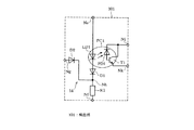
図4は、本実施形態のクランプ部を示している。図4に示すように、トランジスタM21、M22は、Pチャネル型のパワーMOSFETであり、それぞれドレイン・ソース間に接続されたボディダイオードBD21、BD22を備えている。トランジスタM21、M22は、ドレイン・ソース間の耐圧実力値(実力耐圧)が1000V程度のものを選定して使用している。
(Second Embodiment)
Hereinafter, a second embodiment in which the configuration of the clamp portion is changed with respect to the first embodiment will be described with reference to FIG.
FIG. 4 shows the clamp part of this embodiment. As shown in FIG. 4, the transistors M21 and M22 are P-channel type power MOSFETs, each having body diodes BD21 and BD22 connected between the drain and source. The transistors M21 and M22 are selected and used with a drain-source breakdown voltage capability value (effective breakdown voltage) of about 1000V.
トランジスタM21、M22は、いずれもゲート・ソース間が短絡されており、通常はオフ状態に固定されている。トランジスタM21、M22は、各ドレインが互いに接続されている。トランジスタM21のソースはノードNaに接続され、トランジスタM22のソースはノードNbに接続されている。このような構成のクランプ部21をサージ電圧抑制装置7〜9におけるクランプ部10に代えて用いた場合であっても、第1の実施形態と同様の作用および効果が得られる。
In each of the transistors M21 and M22, the gate and the source are short-circuited and are normally fixed in an off state. The drains of the transistors M21 and M22 are connected to each other. The source of the transistor M21 is connected to the node Na, and the source of the transistor M22 is connected to the node Nb. Even when the
(第3の実施形態)
以下、第1の実施形態に対し、検出部の構成を変更した第3の実施形態について図5を参照しながら説明する。
図5は、第1の実施形態における図2相当図であり、上記各実施形態と同一部分には同一符号を付して説明を省略する。本実施形態の検出部31は、第1の実施形態の検出部12に対し、ダイオードD2が省略されている点が異なる。また、発光ダイオードLD1、ダイオードD1および抵抗R1の接続状態が変更されている。すなわち、ノードNeとノードNgの間に、フォトカプラPC1の発光ダイオードLD1、ダイオードD1、抵抗R1が直列に接続されている。本実施形態では、ダイオードD1および抵抗R1により検出電流供給部32が構成されている。
(Third embodiment)
Hereinafter, a third embodiment in which the configuration of the detection unit is changed with respect to the first embodiment will be described with reference to FIG.
FIG. 5 is a view corresponding to FIG. 2 in the first embodiment. The same reference numerals are given to the same parts as those in the above-described embodiments, and the description thereof will be omitted. The
このような構成によれば、トランジスタM1、M2が故障して短絡状態となり、ヒューズF1が溶断すると、端子P1、発光ダイオードLD1、抵抗R1、トランジスタM1、ボディダイオードBD2、端子P2という経路で電流が流れ得る状態となる。従って、上記構成では、このような場合においてはクランプ部10の故障状態を検出できるので、検出部31の構成を簡素化しつつ、第1の実施形態と同様の効果が得られる。
According to such a configuration, when the transistors M1 and M2 fail and are short-circuited, and the fuse F1 is blown, current flows through the path of the terminal P1, the light emitting diode LD1, the resistor R1, the transistor M1, the body diode BD2, and the terminal P2. It will be in a state where it can flow. Therefore, in the above configuration, since the failure state of the
上記構成では、以下のような場合にはクランプ部10の故障状態を検出することができない。すなわち、トランジスタM1、M2が故障して一旦短絡状態となり、ヒューズF1が溶断する前に開放モードでの故障に移行した場合には、発光ダイオードLD1を通じた経路に電流を流すことができない。従って、クランプ部10が開放状態で故障しているにもかかわらず、その状態を検出することができない。ただし、本実施形態における上記問題点については、ヒューズF1として、一層早く溶断するタイプのものを用いることで解消可能である。
In the above configuration, the failure state of the
(第4の実施形態)
以下、第1の実施形態に対し、検出部の構成を変更した第4の実施形態について図6を参照しながら説明する。
図6は、本実施形態の検出部の構成を示しており、上記各実施形態と同一部分には同一符号を付して説明を省略する。本実施形態の検出部41は、第1の実施形態の検出部12に対し、フォトカプラPC1に代えてフォトカプラPC41を備えている点と、新たに抵抗R41を備えている点とが異なる。
(Fourth embodiment)
Hereinafter, a fourth embodiment in which the configuration of the detection unit is changed with respect to the first embodiment will be described with reference to FIG.
FIG. 6 shows the configuration of the detection unit of the present embodiment, and the same parts as those of the above-described embodiments are denoted by the same reference numerals and description thereof is omitted. The
フォトカプラPC41は、サイリスタ出力型のものであり、その受光素子であるフォトサイリスタPT41のゲート・カソード間には抵抗R41が接続されている。抵抗R41は、発光ダイオードLD1が発光したときに流れるゲート電流を制限するとともに、発光ダイオードLD1が発光していない期間に確実にゲート電流を流さないようにするために設けられている。フォトサイリスタPT41のアノードは、ノードNiに接続されている。フォトサイリスタPT41のカソードは、ノードNjに接続されるとともに抵抗R2を介してノードNkに接続されている。 The photocoupler PC41 is of a thyristor output type, and a resistor R41 is connected between the gate and cathode of a photothyristor PT41 which is a light receiving element. The resistor R41 is provided to limit the gate current that flows when the light emitting diode LD1 emits light and to ensure that the gate current does not flow during a period when the light emitting diode LD1 does not emit light. The anode of the photothyristor PT41 is connected to the node Ni. The cathode of the photothyristor PT41 is connected to the node Nj and to the node Nk via the resistor R2.
上記構成の検出部41をサージ電圧抑制装置7〜9の検出部12に代えて用いた場合には以下のような検出動作となる。すなわち、トランジスタM1、M2の故障に起因してヒューズF1が溶断すると、端子P1、発光ダイオードLD1、ダイオードD1、抵抗R1、端子P2という経路で電流が流れる。これにより、発光ダイオードLD1が発光してフォトサイリスタPT41にゲート電流が供給される。これにより、フォトサイリスタPT41がターンオンする。この状態は、ゲート電流の供給状態にかかわらず、フォトサイリスタPT41のアノード・カソード間に流れる電流が一定値以下になるまで継続される。従って、フォトサイリスタPT41がターンオンした後は、直流電圧Vccの供給が停止されるまで、ノードNjの電圧がノードNiの電圧に等しくなる状態が維持される。すなわち、サージ電圧抑制装置7〜9からインバータ2に対し、連続的に故障検出信号が出力される。
When the
このような構成の検出部41を用いた場合、インバータ2の制御部6は、端子Voの電圧を検出し、その電圧レベルがHレベルであるか否かの判断を行うだけで、サージ電圧抑制装置7〜9の故障状態を判断することができる。このため、制御部6において端子Voの電圧の立ち上がりを検出するラッチ回路を省略することができる。従って、本実施形態によれば、第1の実施形態と同様の効果が得られるとともに、第1の実施形態と比べて制御部6の構成および制御内容を簡素化することができる。
When the
(第5の実施形態)
以下、第1の実施形態に対し、検出部の構成を変更した第5の実施形態について図7を参照しながら説明する。
図7は、本実施形態の検出部の構成を示しており、上記各実施形態と同一部分には同一符号を付して説明を省略する。本実施形態の検出部51は、第1の実施形態の検出部12に対し、フォトカプラPC1に代えてフォトカプラPC51を備えている点と、新たに抵抗R51およびサイリスタ52を備えている点とが異なる。
(Fifth embodiment)
Hereinafter, a fifth embodiment in which the configuration of the detection unit is changed with respect to the first embodiment will be described with reference to FIG.
FIG. 7 shows the configuration of the detection unit of the present embodiment, and the same parts as those of the above-described embodiments are denoted by the same reference numerals and description thereof is omitted. The
フォトカプラPC51は、高速のIC出力型のものであり、その受光素子であるフォトIC53には、ノードNi、Nkを介して直流電圧Vccが供給されている。フォトIC53の出力信号は、電流制限用の抵抗R51を介してサイリスタ52のゲートに与えられる。サイリスタ52のアノードは、ノードNiに接続されている。サイリスタ52のカソードは、ノードNjに接続されるとともに抵抗R2を介してノードNkに接続されている。
The photocoupler PC51 is of a high-speed IC output type, and a DC voltage Vcc is supplied to the
上記構成の検出部51をサージ電圧抑制装置7〜9の検出部12に代えて用いた場合には以下のような検出動作となる。すなわち、トランジスタM1、M2の故障に起因してヒューズF1が溶断すると、端子P1、発光ダイオードLD1、ダイオードD1、抵抗R1、端子P2という経路で電流が流れる。これにより、フォトIC53から抵抗R51を通じてサイリスタ52にゲート電流が供給され、サイリスタ52がターンオンする。この状態は、ゲート電流の供給状態にかかわらず、サイリスタ52のアノード・カソード間に流れる電流が一定値以下になるまで継続される。従って、サイリスタ52がターンオンした後は、直流電圧Vccの供給が停止されるまで、ノードNjの電圧がノードNiの電圧に等しくなる状態が維持される。すなわち、サージ電圧抑制装置7〜9からインバータ2に対し、連続的に故障検出信号が出力される。
When the
従って、このような本実施形態の構成によっても、第4の実施形態と同様の作用および効果が得られる。さらに、フォトカプラPC51は、高速のIC出力型のものであるので、発光ダイオードLD1を通じて電流が流れる期間が短くてもサイリスタ52をターンオンさせ、故障検出信号を出力することができる。これにより、インバータ2の出力電圧のパルス幅が狭くなる低速運転時や低キャリア周波数設定時などにおいても、サージ電圧抑制装置7〜9の故障状態を検出することが可能となる。
Therefore, the same operation and effect as the fourth embodiment can be obtained by the configuration of the present embodiment. Further, since the photocoupler PC51 is of a high-speed IC output type, the
(第6の実施形態)
以下、第1の実施形態に対し、検出部の構成を変更した第6の実施形態について図8を参照しながら説明する。
図8は、本実施形態の検出部の構成を示しており、上記各実施形態と同一部分には同一符号を付して説明を省略する。本実施形態の検出部61は、第1の実施形態の検出部12に対し、抵抗R2に代えて抵抗R61を備えている点が異なる。
(Sixth embodiment)
Hereinafter, a sixth embodiment in which the configuration of the detection unit is changed with respect to the first embodiment will be described with reference to FIG.
FIG. 8 shows the configuration of the detection unit of the present embodiment, and the same parts as those of the above-described embodiments are denoted by the same reference numerals and description thereof is omitted. The
フォトダイオードPD1のカソードとトランジスタT1のコレクタとは共通に接続されている。トランジスタT1のコレクタは、ノードNjに接続されるとともに、抵抗R61を介してノードNiに接続されている。トランジスタT1のエミッタは、ノードNkに接続されている。抵抗R61は、トランジスタT1のコレクタ電流を制限するとともに、トランジスタT1がオフしている期間にノードNjの電位をノードNiの電位に固定するプルアップ抵抗である。 The cathode of the photodiode PD1 and the collector of the transistor T1 are connected in common. The collector of the transistor T1 is connected to the node Nj and to the node Ni through the resistor R61. The emitter of the transistor T1 is connected to the node Nk. The resistor R61 is a pull-up resistor that limits the collector current of the transistor T1 and fixes the potential of the node Nj to the potential of the node Ni while the transistor T1 is off.
本実施形態では、トランジスタT1がオンして端子Voの電圧が端子Nの電圧(接地電位=Lレベル)と等しくなる状態が故障検出信号が出力された状態に相当する。また、トランジスタT1がオフして端子Voの電圧が端子Vccの電圧(直流電圧Vcc=Hレベル)と等しくなる状態が故障検出信号が出力されない状態に相当する。 In the present embodiment, the state in which the transistor T1 is turned on and the voltage at the terminal Vo becomes equal to the voltage at the terminal N (ground potential = L level) corresponds to the state in which the failure detection signal is output. A state in which the transistor T1 is turned off and the voltage at the terminal Vo becomes equal to the voltage at the terminal Vcc (DC voltage Vcc = H level) corresponds to a state in which no failure detection signal is output.
また、インバータ2の制御部6は、ラッチ回路を用いて入力される各端子Voの電圧の立ち下がりを検出し、その立ち上がりを所定回数だけ検出すると、それに対応するサージ電圧抑制装置から故障検出信号が与えられたと判断し、所定の故障対応制御を実行するように構成されている。
Further, the
上記構成のように、故障検出信号の出力ノードである検出部61のノードNj(端子Vo)をプルアップする構成とした場合でも、故障検出信号の出力ノードをプルダウンする構成とした第1の実施形態と同様の作用および効果が得られる。なお、図6および図7に示した検出部41、51についても、本実施形態と同様にノードNjをプルアップする構成に変更することができる。
As in the above configuration, even when the node Nj (terminal Vo) of the
(第7の実施形態)
以下、第1の実施形態に対し、検出部の構成を変更した第7の実施形態について図9および図10を参照しながら説明する。
図9は、本実施形態の検出部の構成を示しており、上記各実施形態と同一部分には同一符号を付して説明を省略する。本実施形態の検出部71は、第1の実施形態の検出部12に対し、フォトカプラPC1および抵抗R2に代えて抵抗R71(抵抗素子に相当)および温度リレーTR71(信号出力部に相当)を備えている点とが異なる。
(Seventh embodiment)
Hereinafter, a seventh embodiment in which the configuration of the detection unit is changed with respect to the first embodiment will be described with reference to FIGS. 9 and 10.
FIG. 9 shows the configuration of the detection unit of the present embodiment, and the same parts as those of the above-described embodiments are denoted by the same reference numerals and description thereof is omitted. The
ノードNeとノードNfの間には、抵抗R71、ダイオードD1、抵抗R1が直列に接続されている。温度リレーTR71は、抵抗R71の近傍に設けられる温度検出素子(図示せず)と、その温度検出素子による検出温度が所定温度以上になると作動(閉鎖)する常開形の接点S71(A接点)とを備えている。すなわち、温度リレーTR71は、抵抗R71の温度が所定温度以上になると、その接点S71が閉じる。接点S71の両端子は、それぞれノードNl、Nmに接続されている。 A resistor R71, a diode D1, and a resistor R1 are connected in series between the node Ne and the node Nf. The temperature relay TR71 is a temperature detection element (not shown) provided in the vicinity of the resistor R71, and a normally open contact S71 (contact A) that operates (closes) when the temperature detected by the temperature detection element exceeds a predetermined temperature. And. That is, the contact S71 of the temperature relay TR71 closes when the temperature of the resistor R71 becomes equal to or higher than a predetermined temperature. Both terminals of the contact S71 are connected to nodes Nl and Nm, respectively.
ノードNl、Nmは、インバータ2の制御部6の接点入力端子(図示せず)に接続されている。制御部6は、接点入力端子に接続されるノードNl、Nmの接点信号に基づいて接点S71の作動状態を検出する回路を備えている(図示せず)。例えば、制御部6は、ノードNl、Nmの各接点信号が同電位である場合に接点S71が作動状態であると判断する。なお、本実施形態では、ダイオードD1、D2、抵抗R1、R71により検出電流供給部72が構成される。また、温度リレーTR71の接点S71が閉じた状態が、故障検出信号が出力された状態に相当する。
The nodes Nl and Nm are connected to a contact input terminal (not shown) of the
上記構成の検出部71をサージ電圧抑制装置7〜9の検出部12に代えて用いた場合には以下のような検出動作となる。すなわち、トランジスタM1、M2の故障に起因してヒューズF1が溶断すると、端子P1、抵抗R71、ダイオードD1、抵抗R1、端子P2という経路で電流が断続的に流れる。これに応じて、抵抗R71の温度が次第に上昇し、その温度が所定温度以上になると、温度リレーTR71の接点S71が閉じる。この状態は、抵抗R71の温度が所定温度未満になるまで継続される。すなわち、サージ電圧抑制装置7〜9からインバータ2に対し、連続的に故障検出信号が出力される。制御部6は、ノードNl、Nmの接点信号に基づいて接点S71が作動状態であることを検出すると、サージ電圧抑制装置が故障状態であると判断し、所定の故障対応制御を実行する。
When the
従って、このような本実施形態の構成によっても、第1の実施形態と同様の作用および効果が得られる。さらに、故障検出信号が連続的に出力されるので、それを入力する制御部6の入力部の構成を簡単化することができる。また、検出部71は、外部から電源供給を受けることなく動作可能であるので、第1の実施形態の検出部12などにおいて必要であった直流電圧Vccを供給する必要が無くなる。
Therefore, the same operation and effect as those of the first embodiment can be obtained also by the configuration of the present embodiment. Furthermore, since the failure detection signal is continuously output, the configuration of the input unit of the
また、検出部71をサージ電圧抑制装置7〜9に適用する場合、各ノードNl、Nmを図10のように接続してもよい。図10は、第1の実施形態における図1相当図である。図10では、サージ電圧抑制装置7〜9について接点S71以外の構成の図示は省略している。この図10に示すように、サージ電圧抑制装置7〜9の各ノードNlを共通に接続するとともに、各ノードNmを共通に接続する。すなわち、サージ電圧抑制装置7〜9の各接点S71を互いに並列に接続する。これら共通接続したノードNl、Nmを、インバータ2の制御部6の接点入力端子に接続する。
Moreover, when applying the
この場合、制御部6は、以下のような故障検出を行えばよい。すなわち、サージ電圧抑制装置7〜9の少なくともいずれか1つから故障検出信号が出力された場合、つまり少なくともいずれか1つの接点S71が閉じた場合には、共通接続したノードNl、Nmの各接点信号は同電位となる。制御部6は、ノードNl、Nmの接点信号が同電位である場合にサージ電圧抑制装置7〜9の少なくともいずれか1つが故障状態であると判断し、所定の故障対応制御を実行すればよい。なお、この場合、サージ電圧抑制装置7〜9の各温度リレーTR71の接点S71のうち、少なくとも1つが閉じた状態が、故障検出信号が出力された状態に相当する。
In this case, the
(第8の実施形態)
以下、第1の実施形態に対し、検出部の構成を変更した第8の実施形態について図11および図12を参照しながら説明する。
図11は、本実施形態の検出部の構成を示しており、上記各実施形態と同一部分には同一符号を付して説明を省略する。本実施形態の検出部81は、第7の実施形態の検出部71に対し、温度リレーTR71に代えてサーミスタTH81を備えている点が異なる。
(Eighth embodiment)
Hereinafter, an eighth embodiment in which the configuration of the detection unit is changed with respect to the first embodiment will be described with reference to FIGS. 11 and 12.
FIG. 11 shows the configuration of the detection unit of the present embodiment, and the same parts as those of the above-described embodiments are denoted by the same reference numerals and description thereof is omitted. The
サーミスタTH81は、抵抗R71の近傍に配置されている。これにより、抵抗R71の温度変化に応じてサーミスタTH81の抵抗値が変化する。サーミスタTH81の両端子は、それぞれノードNl、Nmに接続されている。制御部6は、ノードNl、Nm間の抵抗値を検出する抵抗値検出回路を備えている(図示せず)。この抵抗値検出回路は、例えば、ノードNl、Nm間に一定の電流を流し、その際にノードNl、Nm間に生じる電圧の値からサーミスタTH81の抵抗値を検出する。この場合、抵抗R71の温度が所定温度(例えば通常動作においては有り得ないような高い温度)であるときのサーミスタTH81の抵抗値を測定しておき、その所定の抵抗値を故障判定のしきい値として用いればよい。なお、本実施形態では、サーミスタTH81の抵抗値が所定の抵抗値以下になった状態が、故障検出信号が出力された状態に相当する。
The thermistor TH81 is disposed in the vicinity of the resistor R71. Thereby, the resistance value of the thermistor TH81 changes according to the temperature change of the resistor R71. Both terminals of the thermistor TH81 are connected to nodes Nl and Nm, respectively. The
上記構成の検出部81をサージ電圧抑制装置7〜9の検出部12に代えて用いた場合には以下のような検出動作となる。すなわち、トランジスタM1、M2の故障に起因してヒューズF1が溶断すると、抵抗R71に断続的に電流が流れて温度が上昇する。抵抗R71の温度が所定温度以上になると、サーミスタTH81の抵抗値が所定の抵抗値以下となる。この状態は、抵抗R71の温度が所定温度未満になるまで継続される。すなわち、サージ電圧抑制装置7〜9からインバータ2に対し、連続的に故障検出信号が出力される。制御部6は、ノードNl、Nm間の抵抗が所定の抵抗値以下になっていることを検出すると、サージ電圧抑制装置が故障状態であると判断し、所定の故障対応制御を実行する。
When the
従って、このような本実施形態の構成によっても、第1の実施形態と同様の作用および効果が得られる。さらに、検出部81は、外部から電源供給を受けることなく動作可能であるので、第1の実施形態の検出部12などにおいて必要であった直流電圧Vccを供給する必要がなくなる。
Therefore, the same operation and effect as those of the first embodiment can be obtained also by the configuration of the present embodiment. Furthermore, since the
また、検出部81をサージ電圧抑制装置7〜9に適用する場合、各ノードNl、Nmを図12のように接続してもよい。図12は、第1の実施形態における図1相当図である。図12では、サージ電圧抑制装置7〜9についてサーミスタTH81以外の構成の図示は省略している。この図12に示すように、サージ電圧抑制装置9のノードNmとサージ電圧抑制装置7のノードNlとを接続し、サージ電圧抑制装置7のノードNmとサージ電圧抑制装置8のノードNlとを接続する。サージ電圧抑制装置9のノードNl、サージ電圧抑制装置8のノードNmを、それぞれインバータ2の制御部6に接続する。すなわち、サージ電圧抑制装置7〜9の各サーミスタTH81を直列に接続する。
Moreover, when applying the
この場合、制御部6は、各サーミスタTH81の直列合成抵抗値を検出することになり、その値に基づいて以下のような故障検出を行えばよい。すなわち、サージ電圧抑制装置7〜9の少なくともいずれか1つから故障検出信号が出力された場合、つまり各サーミスタTH81の直列合成抵抗値が、少なくとも上記所定の抵抗値だけ低下したことを検出すると、サージ電圧抑制装置7〜9の少なくともいずれか1つが故障状態であると判断し、所定の故障対応制御を実行すればよい。なお、この場合、各サーミスタTH81の直列合成抵抗値が、少なくとも所定の抵抗値だけ低下した状態が、故障検出信号が出力された状態に相当する。
In this case, the
(第9の実施形態)
以下、第1の実施形態に対し、検出部の構成を変更した第9の実施形態について図13および図14を参照しながら説明する。
図13は、本実施形態の検出部の構成を示しており、上記各実施形態と同一部分には同一符号を付して説明を省略する。本実施形態の検出部91は、第1の実施形態の検出部12に対し、抵抗R2およびノードNkが省略されている点が異なる。すなわち、トランジスタT1のエミッタは、ノードNjに接続されている。
(Ninth embodiment)
Hereinafter, a ninth embodiment in which the configuration of the detection unit is changed with respect to the first embodiment will be described with reference to FIGS. 13 and 14.
FIG. 13 shows the configuration of the detection unit of the present embodiment, and the same parts as those of the above-described embodiments are denoted by the same reference numerals and description thereof is omitted. The
図14は、第1の実施形態における図3に相当するものであり、モータ制御装置におけるクランプ部の故障検出に係る部分の構成を示している。本実施形態のサージ電圧抑制装置7〜9は、サージ電圧抑制ユニット92として1つにまとめて構成されている。このサージ電圧抑制ユニット92は、抵抗R91および端子P91、端子P92、端子P93を備えている。
FIG. 14 corresponds to FIG. 3 in the first embodiment, and shows a configuration of a portion related to failure detection of the clamp portion in the motor control device. The surge
サージ電圧抑制装置7〜9の各端子Vcc(=各ノードNi)は、いずれもサージ電圧抑制ユニット92の端子P91に接続されている。サージ電圧抑制装置7〜9の各端子Vo(=ノードNj)は、いずれもサージ電圧抑制ユニット92の端子P92に接続されるとともに、抵抗R91を介して端子P93に接続されている。抵抗R91は、サージ電圧抑制装置7〜9の各トランジスタT1のコレクタ電流を制限するとともに、全てのトランジスタT1がオフしている期間に端子P92の電位を端子P93の電位に固定する。すなわち、本実施形態では、1つの抵抗R91が、第1の実施形態において各サージ電圧抑制装置7〜9にそれぞれ設けられた抵抗R2の代わりにプルダウン抵抗として機能する。
Each terminal Vcc (= each node Ni) of the surge
また、本実施形態では、サージ電圧抑制装置7〜9に設けられたトランジスタT1のうち、少なくとも1つがオンして端子P92の電圧が端子P91の電圧(直流電圧Vcc=Hレベル)と等しくなる状態が故障検出信号が出力された状態に相当する。また、全てのトランジスタT1がオフして端子P92の電圧が端子P93の電圧(接地電位=Lレベル)と等しくなる状態が故障検出信号が出力されない状態に相当する。
In the present embodiment, at least one of the transistors T1 provided in the surge
インバータ盤93は、インバータ2や周辺機器などが収容されるものであり、パトランプ94およびリレー95を備えている。リレー95は、励磁コイル95aおよび励磁コイル95aが励磁されると作動する接点95bを備えている。直流電圧Vccの供給端子と接地電位の供給端子との間には、パトランプ94および接点95bが直列に接続されている。励磁コイル95aの一方の端子は接地電位の供給端子に接続されている。
The
サージ電圧抑制ユニット92の端子P91は、インバータ盤93の内部において、直流電圧Vccの供給端子に接続されている。サージ電圧抑制ユニット92の端子P92は、インバータ盤93の内部において、励磁コイル95aの他方の端子に接続されている。サージ電圧抑制ユニット92の端子P93は、インバータ盤93の内部において、接地電位(基準電位)の供給端子に接続されている。このような構成により、インバータ盤93からサージ電圧抑制装置7〜9に対し、接地電位を基準とした直流電圧Vccが供給される。また、サージ電圧抑制ユニット92の端子P92の電圧がインバータ2の制御部6に入力される。
The terminal P91 of the surge
上記構成によれば、サージ電圧抑制装置7〜9のクランプ部10のうち少なくとも1つが故障すると、少なくとも1つのトランジスタT1がオンしてサージ電圧抑制ユニット92の端子P92の電圧が端子P91の電圧と等しくなる。すると、インバータ盤93において、励磁コイル95aの端子間に直流電圧Vccが印加され、接点95bが閉じる。接点95bが閉じることで、パトランプ94の両端に直流電圧Vccが印加され、パトランプ94が点灯する。
According to the above configuration, when at least one of the
以上説明したように、本実施形態では、サージ電圧抑制装置7〜9のうち少なくともいずれか1つが故障状態になると、インバータ盤93においてパトランプ94を点灯させることで、その状態を使用者に報知する。これにより、モータ3端の各相間において生じるサージ電圧を抑制することができない状態のまま、インバータ2の運転が継続されることを防止できる。従って、本実施形態によっても第1の実施形態と同様の効果が得られる。また、サージ電圧抑制装置7〜9の各端子Voを共通接続した上で、サージ電圧抑制ユニット92に設けた1つの抵抗R91によりプルダウンしている(ワイヤードOR接続)。従って、検出部91を構成する部品の点数を削減しつつ、3つのサージ電圧抑制装置7〜9の故障状態をOR条件で検出することができる。
As described above, in this embodiment, when at least one of the surge
(第10の実施形態)
以下、第6の実施形態に対し、検出部の構成を変更した第10の実施形態について図15および図16を参照しながら説明する。
図15は、本実施形態の検出部の構成を示しており、上記各実施形態と同一部分には同一符号を付して説明を省略する。本実施形態の検出部101は、図8に示した第6の実施形態の検出部61に対し、抵抗R61およびノードNiが省略されている点が異なる。すなわち、トランジスタT1のコレクタは、ノードNjに接続されている。
(Tenth embodiment)
Hereinafter, a tenth embodiment in which the configuration of the detection unit is changed with respect to the sixth embodiment will be described with reference to FIGS. 15 and 16.
FIG. 15 shows the configuration of the detection unit of the present embodiment, and the same parts as those of the above-described embodiments are denoted by the same reference numerals and description thereof is omitted. The
図16は、第1の実施形態における図3に相当するものであり、モータ制御装置におけるクランプ部の故障検出に係る部分の構成を示している。サージ電圧抑制装置7〜9の各端子Vo(=各ノードNj)は、いずれもインバータ2の端子P101に接続されている。サージ電圧抑制装置7〜9の各端子N(=ノードNk)は、いずれもインバータ2の端子P102に接続されている。
FIG. 16 corresponds to FIG. 3 in the first embodiment, and shows a configuration of a portion related to the failure detection of the clamp portion in the motor control device. Each terminal Vo (= each node Nj) of the surge
インバータ2において、端子P101は、制御部6に接続されるとともに、抵抗R101を介して直流電圧Vccの供給端子に接続されている。また、端子P102は、接地電位の供給端子に接続されている。抵抗R101は、サージ電圧抑制装置7〜9の各トランジスタT1のコレクタ電流を制限するとともに、全てのトランジスタT1がオフしている期間に各端子Voの電圧を直流電圧Vccに固定する。すなわち、本実施形態では、1つの抵抗R101が、第6の実施形態において各サージ電圧抑制装置7〜9にそれぞれ設けられた抵抗R61の代わりにプルアップ抵抗として機能する。このような構成により、インバータ2からサージ電圧抑制装置7〜9に対し、接地電位を基準とした直流電圧Vccが供給される。また、サージ電圧抑制装置7〜9の共通に接続された端子Voの電圧がインバータ2の制御部6に入力される。
In the
本実施形態では、サージ電圧抑制装置7〜9に設けられたトランジスタT1のうち、少なくとも1つがオンして各端子Voの電圧が端子Nの電圧(接地電位=Lレベル)と等しくなる状態が故障検出信号が出力された状態に相当する。また、全てのトランジスタT1がオフして端子Voの電圧が直流電圧Vcc(=Hレベル)と等しくなる状態が故障検出信号が出力されない状態に相当する。
In the present embodiment, a failure occurs when at least one of the transistors T1 provided in the surge
上記構成によれば、サージ電圧抑制装置7〜9のクランプ部10のうち少なくとも1つが故障すると、少なくとも1つのトランジスタT1がオンして端子Voの電圧がLレベルとなる。インバータ2の制御部6は、端子Voの電圧の立ち下がりを検出すると、サージ電圧抑制装置7〜9のうち少なくともいずれか1つが故障状態であると判断し、所定の故障対応制御を実行する。この故障対応制御としては、例えば以下の2つの制御などが挙げられる。
According to the above configuration, when at least one of the
インバータ2の端子P101が、非常停止信号入力端子として機能するように割り当てられている場合は以下のような制御が実行される。すなわち、インバータ2によりモータ3を駆動している際、サージ電圧抑制装置7〜9のうち少なくともいずれか1つが故障し、端子P101の電圧がLレベルになると、制御部6は、非常停止信号が入力されたと判断する。これにより、制御部6は、ゲート駆動回路5を介してインバータ2の出力を遮断してモータ3の駆動を停止させる(非常停止)。また、制御部6は、表示部15に対し、非常停止を表す‘E’を表示させ、使用者に対して異常を報知する。
When the terminal P101 of the
また、インバータ2の端子P101が、運転準備完了端子(ST端子)として機能するように割り当てられている場合には以下のような制御が実行される。なお、通常、ST端子は、端子電圧がLレベル(入力導通時)にインバータ2の運転を可能とするものであるが、ここでは、この機能を反転して使用する。つまり、端子電圧がHレベル(入力開放時)にインバータ2の運転を可能とする。インバータ2によりモータ3を駆動している際、サージ電圧抑制装置7〜9のうち少なくともいずれか1つが故障し、端子P101の電圧がLレベルになると、制御部6は、インバータ2の運転を行うことができないと判断する。これにより、制御部6は、ゲート駆動回路5からのゲート駆動信号の送出を停止する(フリーラン停止)。また、制御部6は、表示部15に対し、インバータ2の運転を行うことが不可能である(ST信号がオフである)ことを表す‘OFF’を表示させ、使用者に対して異常を報知する。
Further, when the terminal P101 of the
以上説明したように、本実施形態では、サージ電圧抑制装置7〜9のうち少なくともいずれか1つが故障状態になると、モータ3の駆動を停止するとともに、異常状態であることを使用者に報知する。これにより、モータ3端の各相間において生じるサージ電圧を抑制することができない状態で、インバータ2の運転が継続されることを防止できる。従って、本実施形態によっても第1の実施形態と同様の効果が得られる。また、サージ電圧抑制装置7〜9の各端子Voを共通接続した上で、インバータ2に設けた1つの抵抗R101によりプルアップしている(ワイヤードOR接続)。従って、検出部101を構成する部品の点数を削減しつつ、3つのサージ電圧抑制装置7〜9の故障状態をOR条件で検出することができる。
As described above, in the present embodiment, when at least one of the surge
(第11の実施形態)
以下、サージ電圧抑制装置を複数の分離可能なユニットから構成する第11の実施形態について図17を参照しながら説明する。
図17は、本実施形態のモータ制御装置の構成を示しており、上記各実施形態と同一部分には同一符号を付して説明を省略する。モータ制御装置111は、図1に示した第1の実施形態のモータ制御装置1に対し、サージ電圧抑制装置7〜9に代えてサージ電圧抑制装置7A〜9Aを備えている点が異なる。
(Eleventh embodiment)
Hereinafter, an eleventh embodiment in which the surge voltage suppression device is constituted by a plurality of separable units will be described with reference to FIG.
FIG. 17 shows the configuration of the motor control device of the present embodiment, and the same parts as those of the above-described embodiments are denoted by the same reference numerals and description thereof is omitted. The
サージ電圧抑制装置7Aは、クランプ部10および保護部11からなる第1ユニット112と、検出部12からなる第2ユニット113とから構成されている。第1ユニット112の保護部11のノードNcと、第2ユニット113の検出部12のノードNeとは着脱自在に接続される。第1ユニット112におけるクランプ部10のノードNaおよび保護部11のノードNdと、第2ユニット113の検出部12のノードNgとは着脱自在に接続される。第1ユニット112におけるクランプ部10のノードNbと、第2ユニット113の検出部12のノードNfとは着脱自在に接続される。このように、第1ユニット112と第2ユニット113とは、分離可能な状態で接続されている。なお、図17では、サージ電圧抑制装置8A、9Aの構成についての図示は省略しているが、サージ電圧抑制装置7Aと同様に構成されている。
The surge
上記したように、クランプ部10および保護部11からなる第1ユニット112と、検出部12からなる第2ユニット113とによってサージ電圧抑制装置7A〜9Aを構成した場合であっても、第1の実施形態と同様の作用および効果が得られる。さらに、第1ユニット112および第2ユニット113を分離可能な状態で接続するようにしたので、以下のような効果が得られる。
As described above, even if the surge
例えば、上記各実施形態における所定の構成のクランプ部および保護部を備えた第1ユニット112を1種類の基本ユニットとして準備する。そして、上記各実施形態における検出部にそれぞれ対応した構成の第2ユニット113を複数種類のオプションユニットとして準備する。このようにすれば、使用者は、複数種類のオプションユニットの中から希望する検出部を備えたものを選択することができる。さらに、第1ユニットを1種類とすることで、クランプ部および保護部について使用部品および組立作業が共通化され、その結果、サージ電圧抑制装置全体としての製造コストを低減することができる。
For example, the
(第12の実施形態)
以下、第1の実施形態に対し、サージ電圧抑制装置の構成を変更した第12の実施形態について図18を参照しながら説明する。
図18は、本実施形態のサージ電圧抑制装置121の構成を示しており、上記各実施形態と同一部分には同一符号を付して説明を省略する。本実施形態のサージ電圧抑制装置121は、図2に示した第1の実施形態のサージ電圧抑制装置7に対し、保護部11に代えて保護部122を備えている点と、検出部12に代えて検出部123を備えている点とが異なる。
(Twelfth embodiment)
Hereinafter, a twelfth embodiment in which the configuration of the surge voltage suppressor is changed with respect to the first embodiment will be described with reference to FIG.
FIG. 18 shows the configuration of the
保護部122および検出部123は、内部接点(警報接点)付きのヒューズ124により構成されている。ヒューズ124は、速断型のものであり、ヒューズ部124aが溶断すると接点部124bが作動するようになっている。この接点部124bは常開形の接点(A接点)である。ヒューズ部124aの両端子は、それぞれノードNc、Ndに接続されている。接点部125bの両端子は、それぞれノードNn、ノードNoに接続されている。
The
ノードNn、Noは、インバータ2の制御部6の接点入力端子(図示せず)に接続されている。制御部6は、接点入力端子に接続されるノードNn、Noの接点信号に基づいて接点部124bの作動状態を検出する回路を備えている(図示せず)。このように、本実施形態では、ヒューズ部124aにより保護部122が構成され、接点部124bにより検出部123が構成されている。また、接点部124bが作動して閉じた状態が、故障検出信号が出力された状態に相当する。
Nodes Nn and No are connected to contact input terminals (not shown) of the
上記構成のサージ電圧抑制装置121をサージ電圧抑制装置7〜9に代えて用いた場合には以下のような検出動作となる。すなわち、トランジスタM1、M2の故障に起因してヒューズ部124aが溶断すると、接点部124bが閉じる。制御部6は、ノードNn、Noの接点信号に基づいて接点部124bが作動状態であることを検出すると、サージ電圧抑制装置が故障状態であると判断し、所定の故障対応制御を実行する。
When the surge
従って、このような本実施形態の構成によっても、第1の実施形態と同様の作用および効果が得られる。さらに、上記各実施形態と比べ、検出部を構成する部品の点数を大幅に減らすことができる。また、検出部121は、外部から電源供給を受けることなく動作可能であるので、第1の実施形態の検出部12などにおいて必要であった直流電圧Vccを供給する必要が無くなる。
Therefore, the same operation and effect as those of the first embodiment can be obtained also by the configuration of the present embodiment. Furthermore, compared with the above embodiments, the number of parts constituting the detection unit can be greatly reduced. In addition, since the
また、サージ電圧抑制装置121をサージ電圧抑制装置7〜9に代えて用いる場合、ノードNn、Noを図10に示した第7の実施形態のように接続してもよい。すなわち、3つのサージ電圧抑制装置121の各ノードNnを共通に接続するとともに、各ノードNoを共通に接続する。これら共通接続したノードNn、Noを、インバータ2の制御部6の接点入力端子に接続する。そして、制御部6の制御を、第7の実施形態と同様に変更すればよい。このように構成すれば、第7の実施形態と同様の作用および効果が得られる。
Moreover, when using the surge
(第13の実施形態)
以下、第1の実施形態に対し、サージ電圧抑制装置の構成等を変更した第13の実施形態について図19および図20を参照しながら説明する。
図19および図20は、本実施形態のサージ電圧抑制装置およびそれを用いたモータ制御装置の構成を示しており、上記各実施形態と同一部分には同一符号を付して説明を省略する。図19に示すように、サージ電圧抑制装置131は、図2に示した第1の実施形態のサージ電圧抑制装置7に対し、端子P2に代えて端子Pa、Pbを備えている点と、新たに端子Pcを備えている点とが異なる。端子PaにはノードNbが接続され、端子PbにはノードNfが接続され、端子PcにはノードNa、Ndが接続されている。
(13th Embodiment)
Hereinafter, a thirteenth embodiment in which the configuration of the surge voltage suppression device is changed with respect to the first embodiment will be described with reference to FIGS. 19 and 20.
19 and 20 show the configuration of the surge voltage suppression device of this embodiment and the motor control device using the same, and the same parts as those of the above embodiments are given the same reference numerals and the description thereof is omitted. As shown in FIG. 19, the surge
上記構成のサージ電圧抑制装置131およびそれと同様に構成されたサージ電圧抑制装置132、133を、第1の実施形態のサージ電圧抑制装置7〜9に代えて用いる場合、図20に示すような接続形態となる。この図20に示すモータ制御装置134に設けられるサージ電圧抑制装置131〜133は、モータ3端において各相間に発生するサージ電圧を抑制する。
When the surge
サージ電圧抑制装置131において、端子P1は電圧供給線4uに接続され、端子Paはサージ電圧抑制装置132の端子Pcに接続され、端子Pbは電圧供給線4vに接続され、端子Pcはサージ電圧抑制装置133の端子Paに接続されている。サージ電圧抑制装置132において、端子P1は電圧供給線4vに接続され、端子Paはサージ電圧抑制装置133の端子Pcに接続され、端子Pbは電圧供給線4wに接続されている。サージ電圧抑制装置133において、端子P1は電圧供給線4wに接続され、端子Pbは電圧供給線4uに接続されている。
In the
上記接続形態によれば、サージ電圧抑制装置131〜133の各クランプ部10は、以下のようにモータ3端において各相間に発生するサージ電圧を抑制する。電圧供給線4u、4v間には、サージ電圧抑制装置131の保護部11およびクランプ部10、サージ電圧抑制装置132の保護部11が、この順に直列接続されている。従って、サージ電圧抑制装置131のクランプ部10は、電圧供給線4u、4v間に発生するサージ電圧を抑制するように機能する。また、サージ電圧抑制装置131、132の各保護部11により、サージ電圧抑制装置131のクランプ部10の短絡故障に対する保護が図られている。
According to the said connection form, each
電圧供給線4v、4w間には、サージ電圧抑制装置132の保護部11およびクランプ部10、サージ電圧抑制装置133の保護部11が、この順に直列接続されている。従って、サージ電圧抑制装置132のクランプ部10は、電圧供給線4v、4w間に発生するサージ電圧を抑制するように機能する。また、サージ電圧抑制装置132、133の各保護部11により、サージ電圧抑制装置132のクランプ部10の短絡故障に対する保護が図られている。
Between the
電圧供給線4w、4u間には、サージ電圧抑制装置133の保護部11およびクランプ部10、サージ電圧抑制装置131の保護部11が、この順に直列接続されている。従って、サージ電圧抑制装置133のクランプ部10は、電圧供給線4w、4u間に発生するサージ電圧を抑制するように機能する。また、サージ電圧抑制装置131、133の各保護部11により、サージ電圧抑制装置133のクランプ部10の短絡故障に対する保護が図られている。
Between the
このように、本実施形態のサージ電圧抑制装置131〜133によっても、モータ3端において各相間に発生するサージ電圧を抑制できる。また、サージ電圧抑制装置131〜133の各クランプ部10は、それぞれが2つの保護部11により保護される形態となっている。換言すると、サージ電圧抑制装置131〜133の各保護部11は、それぞれが2つのクランプ部10の短絡故障に対する保護動作を行うようになっている。さらに、サージ電圧抑制装置131〜133の各検出部12は、それぞれに対応する保護部11による保護動作の有無を検出する。従って、本実施形態によっても、第1の実施形態と同様の作用および効果が得られる。
As described above, the surge
(その他の実施形態)
なお、本発明は上記し且つ図面に記載した各実施形態に限定されるものではなく、次のような変形または拡張が可能である。
クランプ部10を構成するトランジスタM1、M2の接続位置を入れ替えてもよい。また、クランプ部21を構成するトランジスタM21、M22の接続位置を入れ替えてもよい。すなわち、トランジスタM1(M21)とM2(M22)とは、それぞれのボディダイオードによる整流方向が互いに逆向きとなるように直列に接続されていればよい。
第1の実施形態におけるトランジスタ出力型のフォトカプラとしては、2次側受光素子が集積化されたものに限らずともよく、例えば2次側素子がフォトトランジスタにより構成されたものでもよい。ただし、この場合、2次側素子の応答性能としては、インバータ2の出力周波数に応じて決定される1次側発光素子の点灯期間において、十分に駆動可能な程度の応答性を有する必要がある。
第1〜第8の実施形態における3つのサージ電圧抑制装置7〜9についても、第9の実施形態のように1つのサージ電圧抑制ユニットとしてまとめて構成してもよい。
サージ電圧抑制装置7〜9において使用する直流電圧Vccは、インバータ2や、インバータ盤93以外の装置から供給するようにしてもよい。また、インバータ2の出力電圧(電圧供給線4u〜4wの電圧)を元に直流電圧Vccを生成する構成をサージ電圧抑制装置に付加してもよい。
(Other embodiments)
The present invention is not limited to the embodiments described above and illustrated in the drawings, and the following modifications or expansions are possible.
The connection positions of the transistors M1 and M2 constituting the
The transistor output type photocoupler in the first embodiment is not limited to the one in which the secondary side light receiving element is integrated. For example, the secondary side element may be constituted by a phototransistor. However, in this case, as the response performance of the secondary side element, it is necessary to have a response that can be sufficiently driven during the lighting period of the primary side light emitting element determined according to the output frequency of the
The three surge
The DC voltage Vcc used in the surge
第7の実施形態における接点S71、第12の実施形態における接点部125bは、いずれも常開形の接点(A接点)であったが、これに代えて常閉形の接点(B接点)を用いてもよい。このような常閉形の接点を用いた場合には、3つのサージ電圧抑制装置の各接点を直列に接続し、その両端の接点信号を制御部6に入力すればよい。3つの常閉形接点のうち、少なくともいずれか1つが開放(作動)された場合には、接点信号は非導通状態となる。制御部6は、この接点信号が非導通状態である場合にサージ電圧抑制装置のいずれか1つが故障状態であると判断すればよい。
第8の実施形態において、インバータ2にサーミスタの抵抗値を検出する機能(サーミスタ温度検出機能)が内蔵されている場合にはこれを利用してもよい。このように予め設けられている機能を利用すれば、その分だけ制御部6の構成を簡単化できる。また、抵抗R71の温度変化を検出するためにサーミスタTH81を用いたが、これに限らずともよく、例えば熱電対を用いてもよい。
第7の実施形態において、モータ3に過熱保護用等の温度リレーが内蔵されている場合、その温度リレーの接点と各温度リレーTR71の接点S71とを直列に接続するとよい。このようにすれば、モータ3とインバータ2との間の配線を流用することができる。
The contact S71 in the seventh embodiment and the contact portion 125b in the twelfth embodiment are both normally open contacts (A contacts), but instead use normally closed contacts (B contacts). May be. When such a normally closed contact is used, the contacts of the three surge voltage suppression devices may be connected in series, and contact signals at both ends thereof may be input to the
In the eighth embodiment, when the
In the seventh embodiment, when a temperature relay for overheat protection or the like is built in the
第9の実施形態において、サージ電圧抑制装置7〜9に供給する直流電圧と、パトランプ94に供給する直流電圧とは、互いに別の電源回路により生成してもよい。また、パトランプ94は、直流電圧により点灯するものに限らず、例えば交流電圧により点灯するものを用いてもよい。
上記各実施形態では、3つのサージ電圧抑制装置をモータ3の各相間に接続したが、これに代えて或いはこれに加えて、サージ電圧抑制装置をモータ3の各相と接地との間に接続してもよい。このようにすれば、モータ3端において各相と接地との間に発生するサージ電圧を抑制することができる。
故障検出信号の出力端子である端子Voの電位をプルダウンするための抵抗およびプルアップするための抵抗は、サージ電圧抑制装置側に設ける必要はなく、例えばインバータ側やインバータ盤側に設けることも可能である。
In the ninth embodiment, the DC voltage supplied to the surge
In each of the above embodiments, three surge voltage suppression devices are connected between the phases of the
The resistor for pulling down the potential of the terminal Vo, which is the output terminal of the failure detection signal, and the resistor for pulling up need not be provided on the surge voltage suppressor side, but can be provided, for example, on the inverter side or the inverter panel side. It is.
図面中、1、111、134はモータ制御装置、2はインバータ、3はモータ、4u、4v、4wは電圧供給線(ケーブル)、7〜9、7A〜9A、121、131〜133はサージ電圧抑制装置、10、21はクランプ部、11、122は保護部、12、31、41、51、61、71、81、91、101、123は検出部、14、32、72は検出電流供給部、52はサイリスタ、53はフォトIC、124bは内部接点、BD1、BD2、BD21、BD22はボディダイオード、F1、124はヒューズ、LD1は発光ダイオード、M1、M21はトランジスタ(第1のパワーMOSFET)、M2、M22はトランジスタ(第2のパワーMOSFET)、PC1、PC41、PC51はフォトカプラ、PT41はフォトサイリスタ(サイリスタ)、R71は抵抗(抵抗素子)、S71は接点、T1はトランジスタ、TH81はサーミスタ(信号出力部)、TR71は温度リレー(信号出力部)を示す。
In the drawings, 1, 111, 134 are motor control devices, 2 is an inverter, 3 is a motor, 4u, 4v, 4w are voltage supply lines (cables), 7-9, 7A-9A, 121, 131-133 are surge voltages.
Claims (14)
前記モータ端の各相に対応して設けられ、当該各相の電圧が所定のクランプ電圧を超えて上昇しようとすると当該モータ端から電流を流すことで、当該各相の電圧を前記クランプ電圧に制限するクランプ部と、
前記クランプ部に対応して設けられ、対応する前記クランプ部が短絡故障すると、直ちに当該クランプ部が介在する通電経路を遮断する保護動作を行う保護部と、
前記保護部に対応して設けられ、対応する前記保護部により前記保護動作が行われたことを検出すると、その保護部に対応する前記クランプ部が故障状態であることを表す故障検出信号を外部に出力する検出部とを備え、
前記クランプ部は、
ドレイン・ソース間に内蔵されたボディダイオードを有する第1および第2のパワーMOSFETを備え、
前記第1および第2のパワーMOSFETのゲート・ソース間をそれぞれ短絡するとともに、前記第1のパワーMOSFETと前記第2のパワーMOSFETとを前記ボディダイオードによる整流方向が互いに逆向きとなるように直列に接続して構成されていることを特徴とするサージ電圧抑制装置。 When a motor is driven by a voltage-type PWM inverter, a surge voltage suppressing device that suppresses a surge voltage generated at the motor end,
It is provided corresponding to each phase of the motor end, and when the voltage of each phase exceeds the predetermined clamp voltage, a current is passed from the motor end, so that the voltage of each phase is changed to the clamp voltage. The clamping part to restrict,
A protection part that is provided corresponding to the clamp part, and that performs a protection operation to immediately shut off the energization path in which the clamp part is interposed when the corresponding clamp part is short-circuited;
When detecting that the protection operation is performed by the corresponding protection unit provided corresponding to the protection unit, a failure detection signal indicating that the clamp unit corresponding to the protection unit is in a failure state is externally provided. And a detector for outputting to
The clamp part is
Comprising first and second power MOSFETs having a body diode built in between the drain and source;
The gates and sources of the first and second power MOSFETs are short-circuited, and the first power MOSFET and the second power MOSFET are connected in series so that the rectification directions of the body diodes are opposite to each other. A surge voltage suppressor, characterized in that it is connected to the device.
The surge voltage suppression device according to claim 1 or 2, wherein the clamp part and the protection part are connected in series between each phase of the motor end and ground.
トランジスタ出力型のフォトカプラと、
前記保護動作が行われると、前記フォトカプラの一次側の発光ダイオードに対し順方向の電流を前記モータ端から供給する検出電流供給部とを備え、
前記フォトカプラの二次側のトランジスタがオン状態である期間に前記故障検出信号を出力することを特徴とする請求項1ないし4のいずれかに記載のサージ電圧抑制装置。 The detector is
A transistor output type photocoupler;
When the protection operation is performed, a detection current supply unit that supplies a forward current to the light emitting diode on the primary side of the photocoupler from the motor end,
The surge voltage suppression device according to any one of claims 1 to 4, wherein the failure detection signal is output during a period in which a transistor on the secondary side of the photocoupler is in an on state.
サイリスタ出力型のフォトカプラと、
前記保護動作が行われると、前記フォトカプラの一次側の発光ダイオードに対し順方向の電流を前記モータ端から供給する検出電流供給部とを備え、
前記フォトカプラの二次側のサイリスタがオン状態である期間に前記故障検出信号を出力することを特徴とする請求項1ないし4のいずれかに記載のサージ電圧抑制装置。 The detector is
A thyristor output type photocoupler;
When the protection operation is performed, a detection current supply unit that supplies a forward current to the light emitting diode on the primary side of the photocoupler from the motor end,
The surge voltage suppression device according to any one of claims 1 to 4, wherein the failure detection signal is output during a period when the thyristor on the secondary side of the photocoupler is in an ON state.
高速IC出力型のフォトカプラと、
前記保護動作が行われると、前記フォトカプラの一次側の発光ダイオードに対し順方向の電流を前記モータ端から供給する検出電流供給部と、
前記フォトカプラの二次側のフォトICの出力信号がゲートに与えられるサイリスタとを備え、
前記サイリスタがオン状態である期間に前記故障検出信号を出力することを特徴とする請求項1ないし4のいずれかに記載のサージ電圧抑制装置。 The detector is
High-speed IC output type photocoupler,
When the protection operation is performed, a detection current supply unit that supplies a forward current from the motor end to the light emitting diode on the primary side of the photocoupler;
A thyristor to which an output signal of a photo IC on the secondary side of the photocoupler is applied to a gate;
The surge voltage suppression device according to any one of claims 1 to 4, wherein the failure detection signal is output during a period in which the thyristor is in an on state.
抵抗素子と、
前記保護動作が行われると、前記抵抗素子に対し前記モータ端から電流を供給する検出電流供給部と、
前記抵抗素子の温度が所定温度以上になると前記故障検出信号を出力する信号出力部とを備えていることを特徴とする請求項1ないし4のいずれかに記載のサージ電圧抑制装置。 The detector is
A resistance element;
When the protection operation is performed, a detection current supply unit that supplies current from the motor end to the resistance element;
5. The surge voltage suppression device according to claim 1, further comprising a signal output unit that outputs the failure detection signal when a temperature of the resistance element becomes equal to or higher than a predetermined temperature. 6.
前記検出部は、前記内部接点が作動している期間に前記故障検出信号を出力することを特徴とする請求項4記載の記載のサージ電圧抑制装置。 The fuse includes an internal contact that operates when blown,
The surge voltage suppression device according to claim 4, wherein the detection unit outputs the failure detection signal during a period in which the internal contact is operating.
請求項1ないし12のいずれかに記載のサージ電圧抑制装置とを備えていることを特徴とするモータ制御装置。 A voltage-type PWM inverter that drives the motor via a cable;
A motor control device comprising the surge voltage suppression device according to claim 1.
前記インバータは、前記故障検出信号が与えられると、前記モータの駆動を停止させる故障対応制御を実行することを特徴とする請求項13記載のモータ制御装置。 The surge voltage suppressor sends the failure detection signal to the inverter;
The motor control device according to claim 13, wherein the inverter performs failure handling control for stopping driving of the motor when the failure detection signal is given.
Priority Applications (1)
| Application Number | Priority Date | Filing Date | Title |
|---|---|---|---|
| JP2009232454A JP5452155B2 (en) | 2009-10-06 | 2009-10-06 | Surge voltage suppression device and motor control device |
Applications Claiming Priority (1)
| Application Number | Priority Date | Filing Date | Title |
|---|---|---|---|
| JP2009232454A JP5452155B2 (en) | 2009-10-06 | 2009-10-06 | Surge voltage suppression device and motor control device |
Publications (2)
| Publication Number | Publication Date |
|---|---|
| JP2011083096A JP2011083096A (en) | 2011-04-21 |
| JP5452155B2 true JP5452155B2 (en) | 2014-03-26 |
Family
ID=44076575
Family Applications (1)
| Application Number | Title | Priority Date | Filing Date |
|---|---|---|---|
| JP2009232454A Expired - Fee Related JP5452155B2 (en) | 2009-10-06 | 2009-10-06 | Surge voltage suppression device and motor control device |
Country Status (1)
| Country | Link |
|---|---|
| JP (1) | JP5452155B2 (en) |
Families Citing this family (1)
| Publication number | Priority date | Publication date | Assignee | Title |
|---|---|---|---|---|
| JP7089463B2 (en) * | 2018-12-11 | 2022-06-22 | ルネサスエレクトロニクス株式会社 | Semiconductor devices and semiconductor device systems |
Family Cites Families (7)
| Publication number | Priority date | Publication date | Assignee | Title |
|---|---|---|---|---|
| JPS611220A (en) * | 1984-06-11 | 1986-01-07 | 日本電気株式会社 | Defect detecting circuit of surge voltage absorber |
| JPH0270231A (en) * | 1988-09-02 | 1990-03-09 | Matsushita Electron Corp | Semiconductor protective device |
| JP2766490B2 (en) * | 1988-12-05 | 1998-06-18 | 三菱電機株式会社 | Semiconductor device |
| JPH03164027A (en) * | 1989-11-20 | 1991-07-16 | New Japan Radio Co Ltd | Overcurrent protective circuit |
| JP3244921B2 (en) * | 1994-03-17 | 2002-01-07 | 株式会社東芝 | Inverter device |
| DE602004023293D1 (en) * | 2003-06-30 | 2009-11-05 | Nxp Bv | PROTECTION DEVICE FOR INTEGRATED CIRCUIT ARRANGEMENT |
| JP3742636B2 (en) * | 2003-08-27 | 2006-02-08 | ファナック株式会社 | Surge voltage suppressor |
-
2009
- 2009-10-06 JP JP2009232454A patent/JP5452155B2/en not_active Expired - Fee Related
Also Published As
| Publication number | Publication date |
|---|---|
| JP2011083096A (en) | 2011-04-21 |
Similar Documents
| Publication | Publication Date | Title |
|---|---|---|
| US8841940B2 (en) | System and method for a driver circuit | |
| US6396721B1 (en) | Power converter control device and power converter thereof | |
| US8488283B2 (en) | Load drive device | |
| CN107181420B (en) | Inverter driving device and semiconductor module | |
| JP2006166691A (en) | Semiconductor apparatus for electric power | |
| JP5673449B2 (en) | Semiconductor device | |
| JP2010158109A (en) | Load circuit protection device | |
| JP2017050804A (en) | Semiconductor switch protection circuit | |
| JP2007082036A (en) | Semiconductor integrated circuit device, power supply apparatus, and electric apparatus | |
| CN107466424B (en) | Power module | |
| JP2014155412A (en) | Motor Drive circuit | |
| JP5929959B2 (en) | Load drive device | |
| JP6394036B2 (en) | Driving device for power semiconductor element | |
| JP5953099B2 (en) | Load control and protection system, and operation and use thereof | |
| JP2004129378A (en) | Gate drive circuit for power semiconductor device | |
| KR100689328B1 (en) | Protection apparatus for inverter | |
| JP5452155B2 (en) | Surge voltage suppression device and motor control device | |
| JP2008061339A (en) | Inverter circuit | |
| JP5421049B2 (en) | Surge voltage suppression device and motor control device | |
| EP2405568A1 (en) | Electronic power apparatus for controlling the movement of alternating current (AC) electric motors stopping such motors in a safe way | |
| KR102388544B1 (en) | Over voltage protection circuit for protecting power semiconductor switching device | |
| JP2007174781A (en) | Drive protection device for inverter circuit | |
| JP2008263695A (en) | Inverter circuit | |
| KR20190106181A (en) | Methods for controlling EPS that cuts motor drive power when overcurrent occurs | |
| JP2019047698A (en) | Semiconductor device |
Legal Events
| Date | Code | Title | Description |
|---|---|---|---|
| A621 | Written request for application examination |
Free format text: JAPANESE INTERMEDIATE CODE: A621 Effective date: 20120724 |
|
| A977 | Report on retrieval |
Free format text: JAPANESE INTERMEDIATE CODE: A971007 Effective date: 20130821 |
|
| A131 | Notification of reasons for refusal |
Free format text: JAPANESE INTERMEDIATE CODE: A131 Effective date: 20130827 |
|
| A521 | Written amendment |
Free format text: JAPANESE INTERMEDIATE CODE: A523 Effective date: 20130926 |
|
| TRDD | Decision of grant or rejection written | ||
| A01 | Written decision to grant a patent or to grant a registration (utility model) |
Free format text: JAPANESE INTERMEDIATE CODE: A01 Effective date: 20131203 |
|
| A61 | First payment of annual fees (during grant procedure) |
Free format text: JAPANESE INTERMEDIATE CODE: A61 Effective date: 20131227 |
|
| R150 | Certificate of patent or registration of utility model |
Ref document number: 5452155 Country of ref document: JP Free format text: JAPANESE INTERMEDIATE CODE: R150 Free format text: JAPANESE INTERMEDIATE CODE: R150 |
|
| R250 | Receipt of annual fees |
Free format text: JAPANESE INTERMEDIATE CODE: R250 |
|
| R250 | Receipt of annual fees |
Free format text: JAPANESE INTERMEDIATE CODE: R250 |
|
| R250 | Receipt of annual fees |
Free format text: JAPANESE INTERMEDIATE CODE: R250 |
|
| R250 | Receipt of annual fees |
Free format text: JAPANESE INTERMEDIATE CODE: R250 |
|
| LAPS | Cancellation because of no payment of annual fees |