JP5445895B2 - Manufacturing method of semiconductor device - Google Patents
Manufacturing method of semiconductor device Download PDFInfo
- Publication number
- JP5445895B2 JP5445895B2 JP2008166113A JP2008166113A JP5445895B2 JP 5445895 B2 JP5445895 B2 JP 5445895B2 JP 2008166113 A JP2008166113 A JP 2008166113A JP 2008166113 A JP2008166113 A JP 2008166113A JP 5445895 B2 JP5445895 B2 JP 5445895B2
- Authority
- JP
- Japan
- Prior art keywords
- film
- forming
- substrate
- manufacturing
- gate
- Prior art date
- Legal status (The legal status is an assumption and is not a legal conclusion. Google has not performed a legal analysis and makes no representation as to the accuracy of the status listed.)
- Expired - Fee Related
Links
Images


Classifications
-
- H—ELECTRICITY
- H10—SEMICONDUCTOR DEVICES; ELECTRIC SOLID-STATE DEVICES NOT OTHERWISE PROVIDED FOR
- H10P—GENERIC PROCESSES OR APPARATUS FOR THE MANUFACTURE OR TREATMENT OF DEVICES COVERED BY CLASS H10
- H10P30/00—Ion implantation into wafers, substrates or parts of devices
- H10P30/20—Ion implantation into wafers, substrates or parts of devices into semiconductor materials, e.g. for doping
- H10P30/21—Ion implantation into wafers, substrates or parts of devices into semiconductor materials, e.g. for doping of electrically active species
-
- H—ELECTRICITY
- H10—SEMICONDUCTOR DEVICES; ELECTRIC SOLID-STATE DEVICES NOT OTHERWISE PROVIDED FOR
- H10D—INORGANIC ELECTRIC SEMICONDUCTOR DEVICES
- H10D30/00—Field-effect transistors [FET]
- H10D30/01—Manufacture or treatment
- H10D30/021—Manufacture or treatment of FETs having insulated gates [IGFET]
- H10D30/0223—Manufacture or treatment of FETs having insulated gates [IGFET] having source and drain regions or source and drain extensions self-aligned to sides of the gate
- H10D30/0227—Manufacture or treatment of FETs having insulated gates [IGFET] having source and drain regions or source and drain extensions self-aligned to sides of the gate having both lightly-doped source and drain extensions and source and drain regions self-aligned to the sides of the gate, e.g. lightly-doped drain [LDD] MOSFET or double-diffused drain [DDD] MOSFET
-
- H—ELECTRICITY
- H10—SEMICONDUCTOR DEVICES; ELECTRIC SOLID-STATE DEVICES NOT OTHERWISE PROVIDED FOR
- H10D—INORGANIC ELECTRIC SEMICONDUCTOR DEVICES
- H10D84/00—Integrated devices formed in or on semiconductor substrates that comprise only semiconducting layers, e.g. on Si wafers or on GaAs-on-Si wafers
- H10D84/01—Manufacture or treatment
- H10D84/0123—Integrating together multiple components covered by H10D12/00 or H10D30/00, e.g. integrating multiple IGBTs
- H10D84/0126—Integrating together multiple components covered by H10D12/00 or H10D30/00, e.g. integrating multiple IGBTs the components including insulated gates, e.g. IGFETs
- H10D84/0165—Integrating together multiple components covered by H10D12/00 or H10D30/00, e.g. integrating multiple IGBTs the components including insulated gates, e.g. IGFETs the components including complementary IGFETs, e.g. CMOS devices
- H10D84/017—Manufacturing their source or drain regions, e.g. silicided source or drain regions
-
- H—ELECTRICITY
- H10—SEMICONDUCTOR DEVICES; ELECTRIC SOLID-STATE DEVICES NOT OTHERWISE PROVIDED FOR
- H10D—INORGANIC ELECTRIC SEMICONDUCTOR DEVICES
- H10D84/00—Integrated devices formed in or on semiconductor substrates that comprise only semiconducting layers, e.g. on Si wafers or on GaAs-on-Si wafers
- H10D84/01—Manufacture or treatment
- H10D84/0123—Integrating together multiple components covered by H10D12/00 or H10D30/00, e.g. integrating multiple IGBTs
- H10D84/0126—Integrating together multiple components covered by H10D12/00 or H10D30/00, e.g. integrating multiple IGBTs the components including insulated gates, e.g. IGFETs
- H10D84/0165—Integrating together multiple components covered by H10D12/00 or H10D30/00, e.g. integrating multiple IGBTs the components including insulated gates, e.g. IGFETs the components including complementary IGFETs, e.g. CMOS devices
- H10D84/0184—Manufacturing their gate sidewall spacers
-
- H—ELECTRICITY
- H10—SEMICONDUCTOR DEVICES; ELECTRIC SOLID-STATE DEVICES NOT OTHERWISE PROVIDED FOR
- H10D—INORGANIC ELECTRIC SEMICONDUCTOR DEVICES
- H10D84/00—Integrated devices formed in or on semiconductor substrates that comprise only semiconducting layers, e.g. on Si wafers or on GaAs-on-Si wafers
- H10D84/01—Manufacture or treatment
- H10D84/02—Manufacture or treatment characterised by using material-based technologies
- H10D84/03—Manufacture or treatment characterised by using material-based technologies using Group IV technology, e.g. silicon technology or silicon-carbide [SiC] technology
- H10D84/038—Manufacture or treatment characterised by using material-based technologies using Group IV technology, e.g. silicon technology or silicon-carbide [SiC] technology using silicon technology, e.g. SiGe
-
- H—ELECTRICITY
- H10—SEMICONDUCTOR DEVICES; ELECTRIC SOLID-STATE DEVICES NOT OTHERWISE PROVIDED FOR
- H10P—GENERIC PROCESSES OR APPARATUS FOR THE MANUFACTURE OR TREATMENT OF DEVICES COVERED BY CLASS H10
- H10P30/00—Ion implantation into wafers, substrates or parts of devices
- H10P30/20—Ion implantation into wafers, substrates or parts of devices into semiconductor materials, e.g. for doping
- H10P30/202—Ion implantation into wafers, substrates or parts of devices into semiconductor materials, e.g. for doping characterised by the semiconductor materials
- H10P30/204—Ion implantation into wafers, substrates or parts of devices into semiconductor materials, e.g. for doping characterised by the semiconductor materials into Group IV semiconductors
-
- H—ELECTRICITY
- H10—SEMICONDUCTOR DEVICES; ELECTRIC SOLID-STATE DEVICES NOT OTHERWISE PROVIDED FOR
- H10P—GENERIC PROCESSES OR APPARATUS FOR THE MANUFACTURE OR TREATMENT OF DEVICES COVERED BY CLASS H10
- H10P30/00—Ion implantation into wafers, substrates or parts of devices
- H10P30/20—Ion implantation into wafers, substrates or parts of devices into semiconductor materials, e.g. for doping
- H10P30/225—Ion implantation into wafers, substrates or parts of devices into semiconductor materials, e.g. for doping of a molecular ion, e.g. decaborane
-
- H—ELECTRICITY
- H10—SEMICONDUCTOR DEVICES; ELECTRIC SOLID-STATE DEVICES NOT OTHERWISE PROVIDED FOR
- H10P—GENERIC PROCESSES OR APPARATUS FOR THE MANUFACTURE OR TREATMENT OF DEVICES COVERED BY CLASS H10
- H10P34/00—Irradiation with electromagnetic or particle radiation of wafers, substrates or parts of devices
- H10P34/40—Irradiation with electromagnetic or particle radiation of wafers, substrates or parts of devices with high-energy radiation
-
- H—ELECTRICITY
- H10—SEMICONDUCTOR DEVICES; ELECTRIC SOLID-STATE DEVICES NOT OTHERWISE PROVIDED FOR
- H10P—GENERIC PROCESSES OR APPARATUS FOR THE MANUFACTURE OR TREATMENT OF DEVICES COVERED BY CLASS H10
- H10P95/00—Generic processes or apparatus for manufacture or treatments not covered by the other groups of this subclass
- H10P95/90—Thermal treatments, e.g. annealing or sintering
-
- H—ELECTRICITY
- H10—SEMICONDUCTOR DEVICES; ELECTRIC SOLID-STATE DEVICES NOT OTHERWISE PROVIDED FOR
- H10D—INORGANIC ELECTRIC SEMICONDUCTOR DEVICES
- H10D30/00—Field-effect transistors [FET]
- H10D30/60—Insulated-gate field-effect transistors [IGFET]
- H10D30/601—Insulated-gate field-effect transistors [IGFET] having lightly-doped drain or source extensions, e.g. LDD IGFETs or DDD IGFETs
-
- H—ELECTRICITY
- H10—SEMICONDUCTOR DEVICES; ELECTRIC SOLID-STATE DEVICES NOT OTHERWISE PROVIDED FOR
- H10D—INORGANIC ELECTRIC SEMICONDUCTOR DEVICES
- H10D64/00—Electrodes of devices having potential barriers
- H10D64/01—Manufacture or treatment
- H10D64/021—Manufacture or treatment using multiple gate spacer layers, e.g. bilayered sidewall spacers
Landscapes
- Insulated Gate Type Field-Effect Transistor (AREA)
- Metal-Oxide And Bipolar Metal-Oxide Semiconductor Integrated Circuits (AREA)
- Electrodes Of Semiconductors (AREA)
Description
本発明は半導体素子の製造方法に係り、より詳細には高性能を有するPMOSトランジスタ及びこれを含むCMOSトランジスタの製造方法に関する。 The present invention relates to a method for manufacturing a semiconductor device, and more particularly to a PMOS transistor having high performance and a method for manufacturing a CMOS transistor including the same.
半導体メモリ素子を構成する基本的な単位素子として電界効果MOSトランジスタ(MOSFET、以下、トランジスタ)がある。前記トランジスタは低電圧で高速動作ができ、小型化、集積化する方向に発展しつつある。 There is a field effect MOS transistor (MOSFET, hereinafter, transistor) as a basic unit element constituting a semiconductor memory element. The transistor can operate at a high voltage with a low voltage, and is developing in the direction of miniaturization and integration.
具体的に、前記メモリ素子が高集積化することに応じて素子を形成するためのアクティブ領域の大きさが大幅に減少しつつある。そのため、前記アクティブ領域に形成されるトランジスタのゲートの長さが減少しつつある。このように、トランジスタのゲートの長さが短くなると、チャンネル領域における電界や電位に及ぶソース及びドレインの影響が著しくなり、ゲート電圧によってスイッチング動作を行いにくくなるというショートチャンネル効果が発生する。即ち、前記ゲート長さが短くなることによってチャンネル領域がゲート電圧のみならず、ソース及びドレイン領域の空乏層電荷や電界及び電位分布の影響を大きく受けるようになり、正常的なスイッチング動作が難しくなる。 Specifically, as the memory device is highly integrated, the size of the active region for forming the device is decreasing significantly. Therefore, the length of the gate of the transistor formed in the active region is decreasing. As described above, when the gate length of the transistor is shortened, the influence of the source and drain on the electric field and potential in the channel region becomes significant, and a short channel effect is generated in which the switching operation is difficult to be performed by the gate voltage. That is, as the gate length is shortened, the channel region is greatly affected by not only the gate voltage but also the depletion layer charge, electric field and potential distribution of the source and drain regions, and normal switching operation becomes difficult. .
また、ドレイン電圧が増加するほどドレインの空乏層が比例して増加してドレイン空乏層がソースに近接する。ゲートの長さが短くなるとドレイン空乏層とソース空乏層とが完全に連結されてしまう。この状態では、ドレイン電界がソース側にまで影響を及ぼしソース近傍の拡散電位を低下させるため、チャンネルが形成されていなくてもソースとドレインとの間に電流が流れるようになる。これがパンチスルーという現像である。パンチスルーが発生し出すと、飽和領域でもドレイン電流が飽和されず急激に増加するようになる。 Also, as the drain voltage increases, the drain depletion layer increases proportionally, and the drain depletion layer approaches the source. When the gate length is shortened, the drain depletion layer and the source depletion layer are completely connected. In this state, since the drain electric field affects the source side and the diffusion potential in the vicinity of the source is lowered, a current flows between the source and the drain even if a channel is not formed. This is a development called punch-through. When punch-through begins to occur, the drain current increases rapidly without being saturated even in the saturation region.
このようなショートチャンネル効果はソース/ドレイン領域の接合深さが深いほど、チャンネルドーピングが低いほど深刻になるので、これを減少させるためにソース/ドレインの接合深さを薄く形成しなければならない。このように、ソース/ドレインの接合深さが薄くなることによってソース/ドレイン抵抗が非常に増加する。 The short channel effect becomes more serious as the junction depth of the source / drain region is deeper and the channel doping is lower. Therefore, in order to reduce this, the junction depth of the source / drain must be thin. Thus, the source / drain resistance is greatly increased by reducing the source / drain junction depth.
また、ショートチャンネル効果を防止するための一方法としてソース/ドレインをLDD(Lightly Doped Drain)構造に形成することが挙げられる。半導体素子の高集積化が加速化して多用な半導体製造技術が開発されることに応じて、最近ではLDD領域を形成するために前記ゲート電極の両側壁にゲートスペーサを形成している。 Another method for preventing the short channel effect is to form the source / drain in an LDD (Lightly Doped Drain) structure. In response to the acceleration of high integration of semiconductor elements and the development of various semiconductor manufacturing techniques, recently, gate spacers are formed on both side walls of the gate electrode in order to form LDD regions.
一方、ソース/ドレインの形成は、ソース/ドレイン領域を露出した後、ソース/ドレインイオンをそれぞれドープした後、ドーパントを活性化するために高温の急速熱処理(Rapid Thermal Process;RTP)を進行する。前記急速熱処理の工程時に前記ソース/ドレイン領域の不純物が基板の下、上、及び側方に拡散する。よって、前記ソース/ドレイン領域間の間隔が更に減少するだけでなく、前記ソース/ドレイン領域の不純物の濃度が更に低くなり前記ソース/ドレイン領域の抵抗が増加する。特に、P型不順物であるホウ素の場合、拡散エネルギーが低くて前記基板の上部に拡散しやすいので、トランジスタの動作特性に悪影響を及ぼす。 On the other hand, in the formation of the source / drain, after exposing the source / drain region, doping the source / drain ions, respectively, followed by a rapid thermal process (RTP) to activate the dopant. During the rapid thermal process, impurities in the source / drain regions diffuse below, above and laterally of the substrate. Accordingly, not only the distance between the source / drain regions is further reduced, but also the impurity concentration in the source / drain regions is further reduced, and the resistance of the source / drain regions is increased. In particular, boron, which is a P-type irregular material, has a low diffusion energy and is likely to diffuse into the upper portion of the substrate, thus adversely affecting the operation characteristics of the transistor.
一方、前記トランジスタが使用者が希望するレベルのしきい電圧を有するためには、特定の仕事関数を有する物質でゲート電極を形成しなければならない。しかし、ポリシリコンの場合には前記ポリシリコンにドープされる不純物の導電型によって仕事関数を適切に調節することができるので、ゲート電極として広く用いられる。具体的に、PMOSトランジスタの場合、P型不純物であるホウ素をドープしたポリシリコンをゲート電極に用い、N型トランジスタの場合、N型不純物であるリンまたは砒素をドープしたポリシリコンをゲート電極に用いることができる。このように、前記不純物がドープされたポリシリコンをゲート電極に用いる場合には、前記ゲート電極内に不純物が拡散しないようにして前記不純物の濃度が減少しないことが望ましい。前記PMOSトランジスタのゲート電極内の不純物の濃度が減少すると、ゲート空乏現像が著しくなって電気的にゲート酸化膜の厚さが増加するので、動作特性が悪くなる。 On the other hand, in order for the transistor to have a threshold voltage desired by the user, the gate electrode must be formed of a material having a specific work function. However, in the case of polysilicon, the work function can be appropriately adjusted according to the conductivity type of the impurity doped into the polysilicon, so that it is widely used as a gate electrode. Specifically, in the case of a PMOS transistor, polysilicon doped with boron, which is a P-type impurity, is used as a gate electrode, and in the case of an N-type transistor, polysilicon doped with phosphorus or arsenic, which is an N-type impurity, is used as a gate electrode. be able to. As described above, when the polysilicon doped with the impurity is used for the gate electrode, it is preferable that the impurity concentration is not reduced by preventing the impurity from diffusing in the gate electrode. When the concentration of impurities in the gate electrode of the PMOS transistor is reduced, gate depletion development becomes remarkable and the thickness of the gate oxide film is electrically increased, so that the operating characteristics are deteriorated.
しかし、前記ソース/ドレイン領域及びゲート電極内における不純物は工程の進行期間に繰り返して行われる熱工程によって継続的に拡散するので、前記不純物の拡散を減少させることが容易でない。更に、PMOSトランジスタに用いられるホウ素の場合にはN型不純物であるリンや砒素に比べて相対的に更に速く拡散が行われるので、前記不純物の拡散によってPMOSトランジスタの特性が劣化することを防止することが容易でない。 However, since the impurities in the source / drain regions and the gate electrode are continuously diffused by a thermal process repeatedly performed during the process, it is not easy to reduce the diffusion of the impurities. Further, in the case of boron used in the PMOS transistor, diffusion is performed relatively faster than phosphorus and arsenic which are N-type impurities, so that the characteristics of the PMOS transistor are prevented from deteriorating due to the diffusion of the impurities. It is not easy.
よって、本発明の目的は、高性能を有するPMOSトランジスタを含む半導体素子の製造方法を提供することにある。
本発明の他の目的は、高性能を有するCMOSトランジスタを含む半導体素子の製造方法を提供することにある。
Accordingly, an object of the present invention is to provide a method for manufacturing a semiconductor device including a PMOS transistor having high performance.
Another object of the present invention is to provide a method for manufacturing a semiconductor device including a CMOS transistor having high performance.
前記の目的を達成するための本発明の一実施例による半導体素子の製造方法によると、基板上に導電膜パターンを形成する。前記基板表面及び前記導電膜パターンの表面上に酸化膜を形成する。不純物の拡散に要求されるエネルギーが上昇するように前記酸化膜を表面処理して拡散防止膜を形成する。その後、前記拡散防止膜を通じて前記導電膜パターン両側の基板及び前記導電膜パターンに前記不純物を注入して、前記基板に不純物領域を形成する。 According to a method of manufacturing a semiconductor device according to an embodiment of the present invention for achieving the above object, a conductive film pattern is formed on a substrate. An oxide film is formed on the surface of the substrate and the surface of the conductive film pattern. The oxide film is surface-treated so as to increase the energy required for impurity diffusion to form a diffusion prevention film. Thereafter, the impurity is implanted into the substrate on both sides of the conductive film pattern and the conductive film pattern through the diffusion prevention film to form an impurity region in the substrate.
前記拡散防止膜を形成する段階は、水素、ヘリウム、窒素、アルゴン、酸素、及びオゾンからなる群より選択された少なくとも一種のガスから生成されたプラズマを用いるプラズマ処理を含むことができる。 The step of forming the diffusion barrier layer may include a plasma process using plasma generated from at least one gas selected from the group consisting of hydrogen, helium, nitrogen, argon, oxygen, and ozone.
前記拡散防止膜を形成する段階は、紫外線照射を含むことができる。
前記他の目的を達成するための本発明の一実施例による半導体素子の製造方法によると、基板の第1領域及び第2領域にそれぞれ第1ゲート構造物及び第2ゲート構造物を形成する。前記基板、第1ゲート構造物及び第2ゲート構造物の表面上にシリコン酸化膜を形成する。P型不純物の拡散に要求されるエネルギーが上昇するように前記シリコン酸化膜を表面処理して拡散防止膜を形成する。前記第1及び第2ゲート構造物の両側壁に形成された前記拡散防止膜上にスペーサを形成する。前記第1領域に位置するスペーサ両側の基板にN型不純物を注入して、前記基板の第1領域に第1不純物領域を形成する。前記第2領域に位置するスペーサ両側の基板にP型不純物を注入して、前記基板の第2領域に第2不純物領域を形成する段階と、を含む。
The step of forming the diffusion barrier layer may include ultraviolet irradiation.
According to a method of manufacturing a semiconductor device according to an embodiment of the present invention for achieving the other object, a first gate structure and a second gate structure are formed in a first region and a second region of a substrate, respectively. A silicon oxide film is formed on the surface of the substrate, the first gate structure, and the second gate structure. The silicon oxide film is surface-treated so as to increase the energy required for the diffusion of the P-type impurity, thereby forming a diffusion prevention film. Spacers are formed on the diffusion barrier layers formed on both side walls of the first and second gate structures. N-type impurities are implanted into the substrate on both sides of the spacer located in the first region to form a first impurity region in the first region of the substrate. Injecting P-type impurities into the substrate on both sides of the spacer located in the second region to form a second impurity region in the second region of the substrate.
前記本発明の方法によって半導体素子を形成する場合、前記拡散防止膜によってゲート及びソース/ドレインに含まれているP型不純物の拡散を減少させることができる。よって、前記ゲート及びソース/ドレインに含まれているP型不純物が拡散して、P型不純物の濃度が減少することを防止することができる。このように、前記P型不純物の濃度を維持させることによって、前記ゲートの空乏現像及びソース/ドレインの抵抗増加の問題を減少させることができる。 When a semiconductor device is formed by the method of the present invention, the diffusion prevention film can reduce the diffusion of P-type impurities contained in the gate and source / drain. Therefore, it is possible to prevent the P-type impurity contained in the gate and the source / drain from diffusing and reducing the concentration of the P-type impurity. As described above, by maintaining the concentration of the P-type impurity, it is possible to reduce the problems of depletion development of the gate and increase in resistance of the source / drain.
以下、添付図面を参照して本発明の望ましい実施例を詳細に説明する。 Hereinafter, exemplary embodiments of the present invention will be described in detail with reference to the accompanying drawings.
図1乃至図7は、本発明の実施例1によるPMOSトランジスタの製造方法を示す断面図である。 1 to 7 are sectional views showing a method of manufacturing a PMOS transistor according to the first embodiment of the present invention.
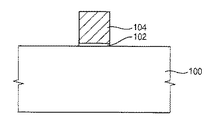
図1を参照すると、前記基板100にゲート酸化膜(図示せず)及びゲート導電膜(図示せず)を順次形成する。前記ゲート酸化膜は、前記基板を熱酸化して形成させたシリコン酸化物で形成することができる。前記ゲート導電膜はP型不純物のドープされたポリシリコン膜で形成することができる。即ち、前記ゲート酸化膜上にポリシリコン膜を形成し、前記ポリシリコン膜に前記P型不純物を注入することで前記ゲート導電膜を形成することができる。ここで、前記P型不純物はホウ素を含む。
Referring to FIG. 1, a gate oxide film (not shown) and a gate conductive film (not shown) are sequentially formed on the
本実施例では、前記ゲート導電膜はP型不純物のドープされたポリシリコン膜のみで形成される。しかし、他の実施例では、前記ゲート導電膜は、前記ポリシリコン膜および金属膜の積層された構造を有することもできる。 In this embodiment, the gate conductive film is formed only of a polysilicon film doped with a P-type impurity. However, in another embodiment, the gate conductive film may have a structure in which the polysilicon film and the metal film are stacked.
その後、フォトリソグラフィ工程を通じて前記ゲート導電膜及びゲート酸化膜をパターニングすることでゲート酸化膜パターン102及びゲートパターン104を形成する。前記ゲートパターン104を形成するためのマスクとしてフォトレジストパターンを用いることもでき、ハードマスクパターンを用いることもできる。前記パターニング工程を行った後、エッチングマスクに用いられたパターンを除去する。
Thereafter, the gate conductive film and the gate oxide film are patterned through a photolithography process to form the gate
前記ゲート酸化膜パターン102及びゲートパターン104の形成された基板を熱酸化させることで、前記基板100及びゲートパターン104の表面上に再酸化膜(図示せず)を形成する。前記再酸化膜を形成することで前記ゲートパターン及び基板の表面がキュアリングされる。前記再酸化膜は、5〜30Åの薄い厚さに形成されることが望ましい。しかし、前記再酸化膜を形成する工程は工程の単純化のために省略してもよい。
A reoxidized film (not shown) is formed on the surface of the
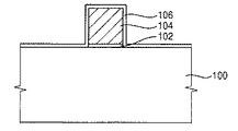
図2を参照すると、前記再酸化膜の形成されている基板100及びゲートパターン104の表面上に第1絶縁膜106を形成する。前記第1絶縁膜106は、後続工程を通じてオフセットスペーサとして提供される。即ち、前記第1絶縁膜の厚さを調節することでソース/ドレインの低濃度のドープ領域の縁部の位置と高濃度のドープ領域の形成位置を調節することができる。前記第1絶縁膜106は、シリコン酸化物を化学気相蒸着法によって10〜30Åの厚さに蒸着して形成することができる。
Referring to FIG. 2, a first
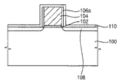
図3を参照すると、前記第1絶縁膜106を異方性エッチングして前記ゲートパターン104の側壁にオフセットスペーサ106aを形成する。前記第1絶縁膜106を異方性エッチングする工程において、前記基板100上に形成されている再酸化膜がともに除去され前記基板100が露出する。
Referring to FIG. 3, the first insulating
その後、前記オフセットスペーサ106aの両側に露出した基板に低濃度の不純物をドープして低濃度ソース/ドレイン領域108を形成する。前記オフセットスペーサ106aが具備されることによって前記低濃度ソース/ドレイン領域108が前記ゲートパターン104の下に拡散しすぎることを防止することができる。
Thereafter, the substrate exposed on both sides of the offset
本実施例では、前記再酸化膜及びオフセットスペーサ106aをそれぞれ形成すると説明したが、前記再酸化膜およびオフセットスペーサ106aのうちのいずれかのみ形成することもできる。また、前記再酸化膜及びオフセットスペーサ106aのいずれも形成しないことも可能である。
In the present embodiment, it has been described that the reoxidized film and the offset
図4を参照すると、前記基板100、オフセットスペーサ106a及び前記ゲートパターン104の表面に沿ってシリコン酸化膜110を形成する。前記シリコン酸化膜110は後続工程でエッチング阻止膜、応力防止のためのパッド膜及び不純物拡散防止膜として用いられる。
Referring to FIG. 4, a
前記シリコン酸化膜は、熱的化学気相蒸着工程によって形成されるO3−TEOS膜から形成することができる。これとは違って、プラズマ強化化学気相蒸着工程または高密度化学気相蒸着工程を通じてシリコン酸化膜を形成することもできる。 The silicon oxide film may be formed from an O 3 -TEOS film formed by a thermal chemical vapor deposition process. In contrast, a silicon oxide film may be formed through a plasma enhanced chemical vapor deposition process or a high density chemical vapor deposition process.
前記シリコン酸化膜110を形成する温度が350℃以下であると化学気相蒸着工程を通じて膜を形成しにくく、前記シリコン酸化膜110を形成する温度が500℃以上であると、基板100及びゲートパターン104が再結晶化するおそれがあるので望ましくない。そのため、前記シリコン酸化膜110を350〜500℃の温度で形成することが望ましい。
If the temperature for forming the
なお、前記シリコン酸化膜110の厚さが20Åより薄いと、後続の窒化膜をエッチングするとき、エッチング阻止膜として用いることが容易でないだけでなく不純物の拡散防止の効果が減少する。反面、シリコン酸化膜110の厚さが100Åより厚いと前記シリコン酸化膜110を通じて基板の下に不純物を注入することが容易でない。よって、前記シリコン酸化膜110を、20〜100Åの厚さに形成することが望ましい。
If the thickness of the
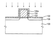
図5を参照すると、前記シリコン酸化膜110に不活性ガス、酸素、及びオゾンガスのうちの少なくとも一つのガスを用いるプラズマ処理を行って前記シリコン酸化膜110を拡散防止膜112に変換させる。前記プラズマ処理に用いることができる前記不活性ガスの例としては、窒素、ヘリウム、水素、アルゴンなどを挙げることができる。
Referring to FIG. 5, the
上述のようにシリコン酸化膜110にプラズマ処理を行うと、前記シリコン酸化膜110の膜質が密になり、膜内に含まれている−OH基または−H基が減少する。そのため、前記拡散防止膜112が形成されている場合は、処理前のシリコン酸化膜110が具備されたときに比べてP型不純物が拡散するのに必要なエネルギーが高くなる。よって、前記P型不純物が前記拡散防止膜を通過して基板の上部に拡散することを最小化することができる。
When plasma treatment is performed on the
具体的には、前記シリコン酸化膜110が熱的化学気相蒸着法によって形成されたO3−TEOS膜である場合、前記O3−TEOS膜内には−OHが複数含まれている。しかし、前記O3−TEOS膜内に不活性ガスを用いるプラズマ処理を行うと、前記O3−TEOS膜内の−OH基の含量が非常に減少するようになる。これとは違って、前記O3−TEOS膜に酸素またはオゾンを用いるプラズマ処理を行うと、前記O3−TEOS膜に酸素結合が強化することによって膜質が密になる。
Specifically, when the
前記プラズマ処理温度が300℃以下であると、プラズマ処理による膜の改質効果が減少する。また、前記プラズマ処理温度が700℃以上であると、非晶質構造を有する基板100及びゲートパターン104が再結晶化するおそれがある。そのため、前記プラズマ処理は300〜700℃の温度で行われることが望ましい。
When the plasma processing temperature is 300 ° C. or lower, the effect of modifying the film by the plasma processing is reduced. If the plasma treatment temperature is 700 ° C. or higher, the
前記プラズマ処理時間が1分以下であると、プラズマ処理による膜の改質効果が減少し、前記プラズマ処理時間が5分以上であると、前記プラズマによって過度に膜が損傷するおそれがあり、工程に所要される時間も過度に長くなって望ましくない。そのため、前記プラズマ処理時間は1〜5分であることが望ましく、前記プラズマ処理温度及び酸化膜の厚さなどによって増減することができる。 If the plasma treatment time is 1 minute or less, the effect of modifying the film by the plasma treatment is reduced, and if the plasma treatment time is 5 minutes or more, the film may be excessively damaged by the plasma. It takes an excessively long time, which is not desirable. Therefore, the plasma processing time is preferably 1 to 5 minutes, and can be increased or decreased depending on the plasma processing temperature and the thickness of the oxide film.
図6を参照すると、前記拡散防止膜112上にスペーサ用絶縁膜(図示せず)を形成する。前記スペーサ用絶縁膜は、前記ゲートパターン104の両側の基板100にドープされる高濃度ソース/ドレイン領域の位置を調節する。前記スペーサ用絶縁膜は、前記拡散防止膜112とエッチング選択比を有するシリコン窒化物で構成することができる。
Referring to FIG. 6, a spacer insulating layer (not shown) is formed on the
具体的には、前記スペーサ用絶縁膜を、プラズマ強化化学気相蒸着(PE−CVD)工程、低圧化学気相蒸着(LPCVD)工程を通じてシリコン窒化膜を蒸着して形成することもできる。前記シリコン窒化膜を蒸着するときの温度が300℃以下であると膜を蒸着しにくく、前記シリコン窒化膜の蒸着温度が500℃以上であると、蒸着中に下部膜に非晶質化した領域の再結晶化が発生して応力が加えられるおそれがあるので望ましくない。そのため、前記シリコン窒化膜の蒸着工程は300〜500℃の温度で行われることが望ましい。 Specifically, the spacer insulating film may be formed by depositing a silicon nitride film through a plasma enhanced chemical vapor deposition (PE-CVD) process or a low pressure chemical vapor deposition (LPCVD) process. When the temperature at which the silicon nitride film is deposited is 300 ° C. or less, it is difficult to deposit the film, and when the deposition temperature of the silicon nitride film is 500 ° C. or more, the region is amorphousized in the lower film during the deposition. This is not desirable because of the risk of stress due to recrystallization. Therefore, it is preferable that the silicon nitride film deposition process is performed at a temperature of 300 to 500 ° C.
前記スペーサ用絶縁膜を蒸着する工程でプラズマを用いる場合には、上述の前記シリコン酸化膜110をプラズマ処理する工程と前記スペーサ用絶縁膜の形成工程をIn Situ(インサイチュ)で行うことができる。例えば、スペーサ用絶縁膜をPE−CVD工程で形成する場合には、上述のプラズマ処理工程を前記PE−CVD工程を行うためのチャンバ内でインサイチュで進行することができる。
In the case where plasma is used in the step of depositing the spacer insulating film, the step of plasma-treating the
その後、前記スペーサ用絶縁膜を異方性エッチングして前記ゲートパターン104の側壁にスペーサ114を形成する。前記エッチング工程で、前記基板100及びゲートパターン104の上部面に形成された拡散防止膜112をエッチング阻止膜に用いて、前記基板100の表面及びゲートパターン104の上部面に形成された拡散防止膜112が露出するようにする。
Thereafter, the spacer insulating film is anisotropically etched to form a
図7を参照すると、前記拡散防止膜112を通過して前記ゲートパターン104の両側の基板にP型不純物を注入することで高濃度のソース/ドレイン領域116を形成する。前記不純物注入の工程時に前記ゲートパターン104内にもP型不純物が注入される。
Referring to FIG. 7, a high concentration source /
これによって、低濃度のソース/ドレイン領域108及び高濃度のソース/ドレイン領域116を含むLDD構造のソース/ドレイン領域118が形成される。
As a result, a source /
その後、前記基板を急速熱処理して前記ソース/ドレイン領域118に形成された不純物を活性化する。前記基板の熱処理は900〜1200℃の温度で窒素、アルゴン、及び水素から選択された少なくとも一つのガス雰囲気下で行うことができる。
Thereafter, the substrate is rapidly heat-treated to activate impurities formed in the source /
図示していないが、前記ソース/ドレイン118領域及びゲートパターン104の上部面に金属シリサイドパターンを形成することができる。
Although not shown, a metal silicide pattern may be formed on the source /
このために、前記基板100表面及びゲートパターン104の上部面に形成されている拡散防止膜112を除去する。その後、前記基板100、スペーサ114、ゲートパターン104の表面に沿って金属膜(図示せず)を形成する。前記金属膜として用いることができる金属物質としてコバルトを挙げることができる。前記金属膜を熱処理して前記金属膜とシリコンとを互いに反応させる。これによって、前記ソース/ドレイン領域とゲートパターンの上部の表面に金属シリサイドパターンが形成される。その後、反応しない金属膜を除去する。
For this, the
このように、金属シリサイドパターンを形成することで前記ゲートパターンおよびソース/ドレインの抵抗を減少させることができる。しかし、工程を単純化するために前記金属シリサイドパターンを形成する工程を省略することもできる。 As described above, by forming the metal silicide pattern, the resistance of the gate pattern and the source / drain can be reduced. However, the process of forming the metal silicide pattern can be omitted to simplify the process.
PMOSトランジスタを形成すると、前記基板を急速熱処理するとき、前記ソース/ドレイン領域及びゲートパターン内に含まれているP型不純物が拡散するおそれがある。しかし、前記ソース/ドレイン領域に該当する基板の表面上に形成されている拡散防止膜によって、前記ソース/ドレイン領域に含まれているP型不純物が基板の上部に拡散することを減少させることができる。また、前記ゲートパターンの側壁及び上部面にも拡散防止膜を具備することで、前記ゲートパターン内に含まれているP型不純物が前記ゲートパターンの上部及び側方を通じて拡散することを減少させることができる。 When a PMOS transistor is formed, P-type impurities contained in the source / drain regions and the gate pattern may diffuse when the substrate is subjected to rapid thermal processing. However, the diffusion prevention film formed on the surface of the substrate corresponding to the source / drain region may reduce the diffusion of P-type impurities contained in the source / drain region to the upper portion of the substrate. it can. In addition, by providing a diffusion prevention film on the sidewall and the upper surface of the gate pattern, it is possible to reduce diffusion of P-type impurities contained in the gate pattern through the upper and side portions of the gate pattern. Can do.
その結果、前記ゲートパターン内に含まれた不純物が拡散によって損失することが抑制されるので、前記ゲートパターン内の不純物濃度を十分に高く維持することができる。そのため、前記ゲートパターンに電圧を印加したとき、前記ゲート酸化膜パターンと隣接している前記ゲートパターンの底面におけるゲート空乏が減少し、これによって電気的にゲート酸化膜パターンの厚さが厚くなることを抑制することができる。なた、チャンネル領域の電荷密度が増加し、電流の密度もまた増加するようになる。 As a result, since the impurities contained in the gate pattern are suppressed from being lost due to diffusion, the impurity concentration in the gate pattern can be maintained sufficiently high. Therefore, when a voltage is applied to the gate pattern, gate depletion at the bottom surface of the gate pattern adjacent to the gate oxide pattern is reduced, thereby electrically increasing the thickness of the gate oxide pattern. Can be suppressed. The charge density in the channel region increases and the current density also increases.
前記ソース/ドレイン領域においても基板の上部にP型不純物が拡散することが抑制されるので、不純物の損失を減少させることができる。よって、前記ソース/ドレイン領域内の不純物の濃度を十分に高く維持することができるので、前記ソース/ドレイン領域の抵抗が減少する効果がある。 Also in the source / drain regions, diffusion of P-type impurities into the upper portion of the substrate is suppressed, so that loss of impurities can be reduced. Therefore, since the impurity concentration in the source / drain region can be maintained sufficiently high, there is an effect that the resistance of the source / drain region is reduced.
図8は、本発明の実施例2によるPMOSトランジスタの製造方法を示す断面図である。 FIG. 8 is a cross-sectional view illustrating a method of manufacturing a PMOS transistor according to the second embodiment of the present invention.
以下で説明する実施例2によるPMOSトランジスタの製造方法は、シリコン酸化膜を拡散防止膜に転換する方法を除いては実施例1と同一である。そのため、重複部分は簡略に説明するかまたは省略する。 The manufacturing method of the PMOS transistor according to the second embodiment described below is the same as that of the first embodiment except for the method of converting the silicon oxide film into the diffusion prevention film. For this reason, overlapping portions will be briefly described or omitted.
まず、実施例1の図1乃至図4を参照して説明したような同一の工程を行う。これによって、基板100にゲート酸化膜パターン102、ゲートパターン104、再酸化膜、オフセットスペーサ106a及びシリコン酸化膜を形成する。
First, the same process as described with reference to FIGS. 1 to 4 of the first embodiment is performed. Thus, the gate
図7を参照すると、前記シリコン酸化膜に紫外線光(UV light)を照射することで前記シリコン酸化膜を改質して拡散防止膜130を形成する。前記紫外線は、100〜500nmの範囲内の波長を有することが望ましく、約200〜300nmの範囲内の波長を有することが更に望ましい。
Referring to FIG. 7, the
具体的には、前記シリコン酸化膜に1〜5分間紫外線光を照射し、ここで、前記基板100を400〜600℃の温度になるようにすることができる。前記紫外線の処理時間が1分以下であると膜の改質効果が減少し、5分以上であると前記紫外線処理によって膜が損傷するおそれがあり、工程に所要される時間も長くなって望ましくない。
Specifically, the silicon oxide film may be irradiated with ultraviolet light for 1 to 5 minutes, and the temperature of the
また、前記シリコン酸化膜に紫外線光を照射する工程は、不活性ガスの雰囲気で行うことができる。前記不活性ガスの例としては、窒素、ヘリウム、水素、アルゴンなどが挙げられる。 The step of irradiating the silicon oxide film with ultraviolet light can be performed in an inert gas atmosphere. Examples of the inert gas include nitrogen, helium, hydrogen, and argon.
上述のように、膜表面に紫外線光を照射する場合、前記紫外線光のエネルギーが前記膜内の分子結合より高くて前記分子結合を切断するようになる。よって、前記紫外線処理を行うと、前記シリコン酸化膜220内に含まれている相対的に結合エネルギーの弱いSi−OH結合、Si−H結合、N−H結合が減少する。よって、前記紫外線処理によって形成された拡散防止膜240は、−OH基または−H基がほぼなく、多くはSi−O結合を有するようになる。 As described above, when the film surface is irradiated with ultraviolet light, the energy of the ultraviolet light is higher than the molecular bond in the film, and the molecular bond is broken. Therefore, when the ultraviolet treatment is performed, Si—OH bonds, Si—H bonds, and N—H bonds, which are contained in the silicon oxide film 220 and have relatively weak binding energy, are reduced. Therefore, the diffusion barrier layer 240 formed by the ultraviolet treatment has almost no —OH group or —H group, and many have Si—O bonds.
よって、前記拡散防止膜130の形成されている場合は、処理前のシリコン酸化膜が具備されたときに比べてP型不純物が拡散するのに必要なエネルギーが高くなる。よって、前記ドープされたP型不純物が基板の上部に拡散することを抑制することができる。
Therefore, when the
図示していないが、前記実施例1でのように前記シリコン酸化膜をプラズマ処理する工程を更に行うこともできる。即ち、前記シリコン酸化膜に前記紫外線光を照射する前または前記紫外線光を照射した後に、前記不活性ガス、酸素、及びオゾンガスのうちの少なくとも一つのガスを用いるプラズマ処理を行うこともできる。 Although not shown, a step of plasma processing the silicon oxide film as in the first embodiment may be further performed. That is, plasma treatment using at least one of the inert gas, oxygen, and ozone gas may be performed before or after the silicon oxide film is irradiated with the ultraviolet light.
その後、図6及び図7を参照して説明したような同一の工程を行うことによってPMOSトランジスタを形成する。前記工程を通じて形成されるPMOSトランジスタも前記ゲートパターン及びソース/ドレイン領域において不純物の拡散が抑制されて良好な動作特性を有する。 Thereafter, the same process as described with reference to FIGS. 6 and 7 is performed to form a PMOS transistor. The PMOS transistor formed through the above process also has good operating characteristics because diffusion of impurities is suppressed in the gate pattern and the source / drain regions.
図9乃至図12は、本発明の実施例3によるCMOSトランジスタの製造方法を示す断面図である。 9 to 12 are sectional views showing a method of manufacturing a CMOS transistor according to the third embodiment of the present invention.
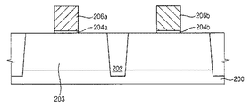
以下で説明する実施例3によるCMOSトランジスタの製造方法は、NMOSトランジスタを形成するための工程が追加されることを除いては実施例1と同一である。よって、重複部分は簡略に説明するかまたは省略する。 The method of manufacturing a CMOS transistor according to the third embodiment described below is the same as that of the first embodiment except that a process for forming an NMOS transistor is added. Thus, overlapping portions will be described briefly or omitted.
図9を参照すると、まず、半導体物質からなる基板200を用意する。前記基板200は、NMOSトランジスタの形成される第1領域とPMOSトランジスタの形成される第2領域とに区分する。
Referring to FIG. 9, first, a
前記基板200にシャロウトレンチ素子分離工程を行って阻止分離膜パターン202を形成することによって、アクティブ領域及びフィールド領域を画定する。
An active region and a field region are defined by performing a shallow trench isolation process on the
その後、NMOS及びPMOSトランジスタそれぞれのチャンネル領域203を形成するために、前記第1領域の基板にP型不純物をドープし、前記第2領域の基板にN型不純物をドープする。
Thereafter, in order to form
具体的には、前記第1領域の基板200を選択的に露出する第1イオン注入マスクパターン(図示せず)を形成した後、前記第1領域の基板にP型不純物をイオン注入する。その後、前記第1イオン注入マスクパターンを除去する。また、前記第2領域の基板200を選択的に露出する第2イオン注入マスクパターン(図示せず)を形成した後、前記第2領域の基板にN型不純物をイオン注入する。その後、前記第2イオン注入マスクパターンを除去する。前記第1及び第2イオン注入マスクパターンは、フォトレジストを用いて形成することができる。前記P型不純物の例としては、ホウ素、BF2などを挙げることができ、前記N型不純物の例としては、砒素、リンなどを挙げることができる。
Specifically, after forming a first ion implantation mask pattern (not shown) that selectively exposes the
その後、前記基板200上にゲート酸化膜(図示せず)を形成する。前記ゲート酸化膜は、前記基板200の表面を熱酸化して形成させることができる。
Thereafter, a gate oxide film (not shown) is formed on the
前記ゲート酸化膜上にゲートで用いるためのポリシリコン膜(図示せず)を形成する。その後、前記第1領域に形成されている前記ポリシリコン膜にはN型不純物を注入し、前記第2領域に形成されている前記ポリシリコン膜にはP型不純物を注入する。このために、前記不純物注入の工程の前に、前記ポリシリコン膜上にイオン注入マスクとしてフォトレジストパターンを形成する工程が行われる。ここで、前記N型不純物はリンまたは砒素を含み、前記P型不純物はホウ素を含む。しかし、現段階において前記ポリシリコン膜に不純物を注入する工程を行わなくても良い。 A polysilicon film (not shown) for use in the gate is formed on the gate oxide film. Thereafter, N-type impurities are implanted into the polysilicon film formed in the first region, and P-type impurities are implanted into the polysilicon film formed in the second region. Therefore, a step of forming a photoresist pattern as an ion implantation mask on the polysilicon film is performed before the impurity implantation step. Here, the N-type impurity includes phosphorus or arsenic, and the P-type impurity includes boron. However, the step of implanting impurities into the polysilicon film does not have to be performed at this stage.
その後、フォトリソグラフィ工程を通じて前記ポリシリコン膜及びゲート酸化膜をパターニングすることで前記第1領域には第1ゲート酸化膜パターン204a及び第1ゲートパターン206aを形成し、前記第2領域に第2ゲート酸化膜パターン204b及び第2ゲートパターン206bを形成する。
Thereafter, the polysilicon film and the gate oxide film are patterned through a photolithography process to form a first
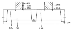
図10を参照すると、前記図2及び図3を参照して説明したような同一の工程を行うことで、前記第1及び第2ゲートパターン(206a、206b)に再酸化膜(図示せず)及びオフセットスペーサ208を形成する。
Referring to FIG. 10, a re-oxidized film (not shown) is formed on the first and
その後、前記第1領域の基板を選択的に露出する第3イオン注入マスクパターン(図示せず)を形成した後、前記第1領域の基板にN型不純物をイオン注入する。前記工程を通じて、NMOSトランジスタの低濃度のソース/ドレイン領域210aが形成される。また、前記N型不純物をイオン注入する工程を行うと、前記第1ゲートパターン206a内にもN型不純物がドープされる。その後、前記第3イオン注入マスクパターンを除去する。
Thereafter, a third ion implantation mask pattern (not shown) that selectively exposes the substrate in the first region is formed, and then N-type impurities are ion-implanted into the substrate in the first region. Through the above process, the low concentration source /
また、前記第2領域の基板200を選択的に露出する第4イオン注入マスクパターン(図示せず)を形成した後、前記第2領域の基板にP型不純物をイオン注入する。前記工程を通じて、PMOSトランジスタの低濃度ソース/ドレイン領域210bが形成される。また、前記P型不純物をイオン注入工程を行うと、前記第2ゲートパターン206bにもP型不純物がドープされる。その後、前記第4イオン注入マスクパターンを除去する。
In addition, after forming a fourth ion implantation mask pattern (not shown) that selectively exposes the
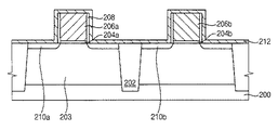
図11を参照すると、前記第1及び第2ゲートパターン(206a、206b)、オフセットスペーサ208及び基板200の表面にシリコン酸化膜を形成する。
その後、前記図5を参照して説明したように、前記シリコン酸化膜に不活性ガス、酸素、及びオゾンガスのうち、少なくとも一種のガスを用いるプラズマ処理を行って前記シリコン酸化膜を拡散防止膜212に変換する。前記プラズマ処理の用いることができる前記不活性ガスの例としては、窒素、ヘリウム、水素、アルゴンなどを挙げることができる。
Referring to FIG. 11, a silicon oxide layer is formed on the surfaces of the first and
Thereafter, as described with reference to FIG. 5, the silicon oxide film is subjected to plasma treatment using at least one of an inert gas, oxygen, and ozone gas, so that the silicon oxide film is prevented from being diffused. Convert to Examples of the inert gas that can be used for the plasma treatment include nitrogen, helium, hydrogen, and argon.
これとは違って、前記図8を参照して説明したように、前記シリコン酸化膜に紫外線光(UV light)を照射することで、前記シリコン酸化膜を改質して拡散防止膜212を形成することもできる。
In contrast, as described with reference to FIG. 8, the silicon oxide film is modified to form a
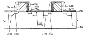
図12を参照すると、前記拡散防止膜212上にスペーサ用絶縁膜を形成し、これを異方性エッチングすることでスペーサ214を形成する。
Referring to FIG. 12, a spacer insulating film is formed on the
その後、前記第1領域の基板を選択的に露出する第5イオン注入マスクパターン(図示せず)を形成した後、前記第1領域の基板にN型不純物をイオン注入する。前記工程を通じて、NMOSトランジスタの高濃度のソース/ドレイン領域216aが形成される。また、前記N型不純物をイオン注入する工程を行うと、前記第1ゲートパターン206aにもN型不純物がドープされる。その後、前記第5イオン注入マスクパターンを除去する。
Thereafter, a fifth ion implantation mask pattern (not shown) for selectively exposing the substrate in the first region is formed, and then N-type impurities are ion-implanted into the substrate in the first region. Through the above process, a high concentration source /
また、前記第2領域の基板200を選択的に露出する第6イオン注入マスクパターン(図示せず)を形成した後、前記第2領域の基板にP型不純物をイオン注入する。前記工程を通じて、PMOSトランジスタの高濃度のソース/ドレイン領域216bが形成される。また、前記P型不純物をイオン注入する工程を行うと、前記第2ゲートパターンにもP型不純物がドープされる。その後、前記第6イオン注入マスクパターンを除去する。
In addition, after forming a sixth ion implantation mask pattern (not shown) that selectively exposes the
その後、急速熱処理工程を通じて、前記ソース/ドレイン領域に含まれた不純物を活性化させる。 Thereafter, impurities included in the source / drain regions are activated through a rapid thermal process.
前記工程を行うと、LDD構造のソース/ドレイン領域を有するCMOSトランジスタが形成される。前記方法によると、ソース/ドレイン領域及びゲートパターンに含まれている不純物が拡散されることが抑制されるので、高性能を有するCMOSトランジスタを形成することができる。 When the above process is performed, a CMOS transistor having an LDD source / drain region is formed. According to the above method, since the impurities contained in the source / drain regions and the gate pattern are suppressed from being diffused, a high-performance CMOS transistor can be formed.
上述したように本発明によると、簡単な工程を通じて不純物の拡散を抑制して高性能を有するトランジスタを形成することができる。具体的には、本発明の方法によって製造されたトランジスタはゲート空乏現像が減少し、ソース/ドレインの抵抗が減少することによって動作電流を増加させて動作速度が速くなる。なお、トランジスタの飽和電流が増加する。これによって、前記トランジスタの動作特性が良好になりかつ信頼性が高くなる。 As described above, according to the present invention, a transistor having high performance can be formed by suppressing diffusion of impurities through a simple process. Specifically, the transistor manufactured by the method of the present invention has a reduced gate depletion development, and an increased operating current due to a reduced source / drain resistance, resulting in a faster operating speed. Note that the saturation current of the transistor increases. As a result, the operational characteristics of the transistor are improved and the reliability is increased.
以上、本発明の実施例によって詳細に説明したが、本発明はこれに限定されず、本発明が属する技術分野において通常の知識を有する者であれば本発明の思想と精神から逸脱することなく、本発明を修正または変更できる。 As described above, the embodiments of the present invention have been described in detail. However, the present invention is not limited thereto, and those who have ordinary knowledge in the technical field to which the present invention belongs can be used without departing from the spirit and spirit of the present invention. The present invention can be modified or changed.
100、200 基板
102 ゲート酸化膜パターン
104 ゲートパターン
106 第1絶縁膜
106a、208 オフセットスペーサ
108、210a、210b 低濃度のソース/ドレイン領域
110、220 シリコン酸化膜
112、130 拡散防止膜
114、214 スペーサ
116、216a、216b 高濃度のソース/ドレイン領域
118 LDD構造のソース/ドレイン領域
203 チャンネル領域
204a 第1ゲート酸化膜パターン
206a 第1ゲートパターン
206b 第2ゲートパターン
212 拡散防止膜
100, 200
Claims (8)
前記基板表面及び前記導電膜パターンの表面上に酸化膜を形成する段階と、
不純物の拡散に要求されるエネルギーが上昇するように前記酸化膜を表面処理して拡散防止膜を形成する段階と、
前記拡散防止膜を通じて前記導電膜パターン両側の基板及び前記導電膜パターンに前記不純物を注入して、前記基板に不純物領域を形成する段階と、を含み、
前記酸化膜を形成する段階は、O3−TEOS膜を形成する熱的化学気相蒸着工程を含み、
前記拡散防止膜を形成する段階は、水素、ヘリウム、及びオゾンからなる群より選択された少なくとも一種のガスから生成されたプラズマを用いるプラズマ処理を含むことを特徴とする半導体素子の製造方法。 Forming a conductive film pattern on the substrate;
Forming an oxide film on the surface of the substrate and the surface of the conductive film pattern;
Forming a diffusion barrier film by surface-treating the oxide film so that energy required for impurity diffusion is increased;
Injecting the impurity into the conductive film pattern on both sides of the conductive film pattern through the diffusion barrier film and forming an impurity region in the substrate,
The step of forming the oxide film includes a thermal chemical vapor deposition process for forming an O 3 -TEOS film,
It said step of forming a diffusion preventing film, hydrogen, helium, a method of manufacturing a semiconductor device characterized in that it comprises a plasma treatment with a plasma generated from at least one gas selected from the group consisting 及 beauty ozone.
前記拡散防止膜をエッチング防止膜に用いて前記スペーサ膜を異方性エッチングすることによって前記導電膜パターンの側壁に位置する拡散防止膜上にスペーサを形成する段階と、を更に含むことを特徴とする請求項1から3の何れか一項に記載の半導体素子の製造方法。 Forming a spacer film on the diffusion barrier film;
Forming a spacer on the diffusion barrier film located on a sidewall of the conductive film pattern by anisotropically etching the spacer film using the diffusion barrier film as an etching barrier film; The manufacturing method of the semiconductor element as described in any one of Claim 1 to 3 .
Applications Claiming Priority (2)
| Application Number | Priority Date | Filing Date | Title |
|---|---|---|---|
| KR1020070064941A KR100846097B1 (en) | 2007-06-29 | 2007-06-29 | Manufacturing Method of Semiconductor Device |
| KR10-2007-0064941 | 2007-06-29 |
Publications (3)
| Publication Number | Publication Date |
|---|---|
| JP2009016824A JP2009016824A (en) | 2009-01-22 |
| JP2009016824A5 JP2009016824A5 (en) | 2011-08-04 |
| JP5445895B2 true JP5445895B2 (en) | 2014-03-19 |
Family
ID=39824476
Family Applications (1)
| Application Number | Title | Priority Date | Filing Date |
|---|---|---|---|
| JP2008166113A Expired - Fee Related JP5445895B2 (en) | 2007-06-29 | 2008-06-25 | Manufacturing method of semiconductor device |
Country Status (3)
| Country | Link |
|---|---|
| US (1) | US7732311B2 (en) |
| JP (1) | JP5445895B2 (en) |
| KR (1) | KR100846097B1 (en) |
Families Citing this family (5)
| Publication number | Priority date | Publication date | Assignee | Title |
|---|---|---|---|---|
| KR101376260B1 (en) * | 2008-04-14 | 2014-03-20 | 삼성전자 주식회사 | Semiconductor device and method for fabricating the same |
| CN102456556A (en) * | 2010-10-18 | 2012-05-16 | 中芯国际集成电路制造(上海)有限公司 | Formation method of metal silicide |
| US9483266B2 (en) | 2013-03-15 | 2016-11-01 | Intel Corporation | Fusible instructions and logic to provide OR-test and AND-test functionality using multiple test sources |
| CN115863404A (en) * | 2022-12-06 | 2023-03-28 | 上海积塔半导体有限公司 | Semiconductor structure and manufacturing method thereof |
| CN118969730B (en) * | 2024-10-16 | 2025-03-04 | 物元半导体技术(青岛)有限公司 | Hybrid bonding method and hybrid bonding structure |
Family Cites Families (16)
| Publication number | Priority date | Publication date | Assignee | Title |
|---|---|---|---|---|
| JP2889295B2 (en) * | 1989-07-17 | 1999-05-10 | 株式会社東芝 | Semiconductor device and manufacturing method thereof |
| JP3359794B2 (en) * | 1994-08-31 | 2002-12-24 | 株式会社半導体エネルギー研究所 | Method for manufacturing semiconductor device |
| US6323519B1 (en) * | 1998-10-23 | 2001-11-27 | Advanced Micro Devices, Inc. | Ultrathin, nitrogen-containing MOSFET sidewall spacers using low-temperature semiconductor fabrication process |
| JP2000269490A (en) * | 1999-03-16 | 2000-09-29 | Fujitsu Ltd | Method for manufacturing semiconductor device |
| JP4582837B2 (en) * | 1999-09-09 | 2010-11-17 | シャープ株式会社 | Manufacturing method of semiconductor device |
| KR100361576B1 (en) | 2000-04-07 | 2002-11-21 | 아남반도체 주식회사 | Method for manufacturing premetal dielectric layer of semiconductor devices |
| US6534388B1 (en) * | 2000-09-27 | 2003-03-18 | Chartered Semiconductor Manufacturing Ltd. | Method to reduce variation in LDD series resistance |
| JP2003077856A (en) * | 2001-06-18 | 2003-03-14 | Matsushita Electric Ind Co Ltd | Method for manufacturing semiconductor device |
| JP2004153037A (en) | 2002-10-31 | 2004-05-27 | Renesas Technology Corp | Method for manufacturing semiconductor device |
| JP2004303789A (en) * | 2003-03-28 | 2004-10-28 | Toshiba Corp | Semiconductor device and manufacturing method thereof |
| KR100610436B1 (en) * | 2003-12-23 | 2006-08-08 | 주식회사 하이닉스반도체 | Method for suppressing deterioration of gate oxide film |
| JP2006019366A (en) * | 2004-06-30 | 2006-01-19 | Canon Inc | Method for forming insulating film of semiconductor device |
| JP2006049779A (en) * | 2004-08-09 | 2006-02-16 | Renesas Technology Corp | Semiconductor device and its manufacturing method |
| KR20060037776A (en) * | 2004-10-28 | 2006-05-03 | 주식회사 하이닉스반도체 | Method for manufacturing a semiconductor device having a gate spacer by atomic layer deposition |
| KR100668954B1 (en) | 2004-12-15 | 2007-01-12 | 동부일렉트로닉스 주식회사 | Method of manufacturing thin film transistor |
| KR20070043108A (en) * | 2005-10-20 | 2007-04-25 | 삼성전자주식회사 | Semiconductor device manufacturing method |
-
2007
- 2007-06-29 KR KR1020070064941A patent/KR100846097B1/en not_active Expired - Fee Related
-
2008
- 2008-06-20 US US12/213,502 patent/US7732311B2/en not_active Expired - Fee Related
- 2008-06-25 JP JP2008166113A patent/JP5445895B2/en not_active Expired - Fee Related
Also Published As
| Publication number | Publication date |
|---|---|
| JP2009016824A (en) | 2009-01-22 |
| US20090004800A1 (en) | 2009-01-01 |
| KR100846097B1 (en) | 2008-07-14 |
| US7732311B2 (en) | 2010-06-08 |
Similar Documents
| Publication | Publication Date | Title |
|---|---|---|
| JP4469677B2 (en) | Semiconductor device and manufacturing method thereof | |
| JP4313065B2 (en) | Semiconductor device using silicon germanium gate and manufacturing method thereof | |
| JP5235486B2 (en) | Semiconductor device | |
| JP2897004B2 (en) | CMOSFET manufacturing method | |
| KR100839359B1 (en) | PMOS transistor manufacturing method and complementary MOS transistor manufacturing method | |
| JPH09181307A (en) | Semiconductor device and manufacturing method thereof | |
| US20080054363A1 (en) | Dual gate cmos semiconductor device and method for manufacturing the same | |
| JP5445895B2 (en) | Manufacturing method of semiconductor device | |
| JP4818499B2 (en) | Manufacturing method of semiconductor device | |
| US8247873B2 (en) | Semiconductor device and method for manufacturing the same | |
| CN113540252B (en) | Semiconductor device and method of manufacturing the same | |
| KR100837555B1 (en) | Semiconductor device and manufacturing method thereof | |
| JP4810832B2 (en) | Manufacturing method of semiconductor device | |
| JP4186247B2 (en) | Method for manufacturing semiconductor device and method for forming conductive silicon film | |
| US7785945B2 (en) | Method for fabricating PMOS transistor | |
| JP4746332B2 (en) | Manufacturing method of semiconductor device | |
| KR100588784B1 (en) | Semiconductor device manufacturing method | |
| KR100503743B1 (en) | Method For Manufacturing Semiconductor Devices | |
| KR101051954B1 (en) | Transistor Formation Method of Semiconductor Device | |
| US20080124879A1 (en) | Method for Fabricating Semiconductor Device | |
| KR100546812B1 (en) | Semiconductor device manufacturing method | |
| KR100609235B1 (en) | Manufacturing Method of Semiconductor Device | |
| KR100657754B1 (en) | Manufacturing method of thin junction of semiconductor device | |
| KR100790264B1 (en) | Semiconductor device and method for fabricating the same | |
| KR20060077160A (en) | Method of manufacturing transistor of semiconductor device |
Legal Events
| Date | Code | Title | Description |
|---|---|---|---|
| A521 | Request for written amendment filed |
Free format text: JAPANESE INTERMEDIATE CODE: A523 Effective date: 20110620 |
|
| A621 | Written request for application examination |
Free format text: JAPANESE INTERMEDIATE CODE: A621 Effective date: 20110620 |
|
| A521 | Request for written amendment filed |
Free format text: JAPANESE INTERMEDIATE CODE: A523 Effective date: 20120518 |
|
| A977 | Report on retrieval |
Free format text: JAPANESE INTERMEDIATE CODE: A971007 Effective date: 20130222 |
|
| A131 | Notification of reasons for refusal |
Free format text: JAPANESE INTERMEDIATE CODE: A131 Effective date: 20130226 |
|
| A521 | Request for written amendment filed |
Free format text: JAPANESE INTERMEDIATE CODE: A523 Effective date: 20130521 |
|
| A02 | Decision of refusal |
Free format text: JAPANESE INTERMEDIATE CODE: A02 Effective date: 20130618 |
|
| A521 | Request for written amendment filed |
Free format text: JAPANESE INTERMEDIATE CODE: A523 Effective date: 20131018 |
|
| A911 | Transfer to examiner for re-examination before appeal (zenchi) |
Free format text: JAPANESE INTERMEDIATE CODE: A911 Effective date: 20131108 |
|
| TRDD | Decision of grant or rejection written | ||
| A01 | Written decision to grant a patent or to grant a registration (utility model) |
Free format text: JAPANESE INTERMEDIATE CODE: A01 Effective date: 20131203 |
|
| A61 | First payment of annual fees (during grant procedure) |
Free format text: JAPANESE INTERMEDIATE CODE: A61 Effective date: 20131212 |
|
| R150 | Certificate of patent or registration of utility model |
Free format text: JAPANESE INTERMEDIATE CODE: R150 |
|
| LAPS | Cancellation because of no payment of annual fees |