JP5416228B2 - エレクトロルミネッセント(el)サブピクセル内の駆動トランジスタのゲート電極に駆動トランジスタ制御信号を与えるための装置 - Google Patents
エレクトロルミネッセント(el)サブピクセル内の駆動トランジスタのゲート電極に駆動トランジスタ制御信号を与えるための装置 Download PDFInfo
- Publication number
- JP5416228B2 JP5416228B2 JP2011552987A JP2011552987A JP5416228B2 JP 5416228 B2 JP5416228 B2 JP 5416228B2 JP 2011552987 A JP2011552987 A JP 2011552987A JP 2011552987 A JP2011552987 A JP 2011552987A JP 5416228 B2 JP5416228 B2 JP 5416228B2
- Authority
- JP
- Japan
- Prior art keywords
- current
- voltage
- drive transistor
- emitter
- subpixel
- Prior art date
- Legal status (The legal status is an assumption and is not a legal conclusion. Google has not performed a legal analysis and makes no representation as to the accuracy of the status listed.)
- Active
Links
- 238000005259 measurement Methods 0.000 claims description 118
- 230000008859 change Effects 0.000 claims description 24
- 230000006870 function Effects 0.000 claims description 18
- 238000004519 manufacturing process Methods 0.000 claims description 18
- 230000004044 response Effects 0.000 claims description 11
- 238000012360 testing method Methods 0.000 claims description 11
- 229910021420 polycrystalline silicon Inorganic materials 0.000 claims description 3
- 229920005591 polysilicon Polymers 0.000 claims description 3
- 238000000034 method Methods 0.000 description 31
- 238000006243 chemical reaction Methods 0.000 description 17
- 230000000694 effects Effects 0.000 description 15
- 238000012545 processing Methods 0.000 description 15
- 229910021417 amorphous silicon Inorganic materials 0.000 description 13
- 238000013461 design Methods 0.000 description 13
- 239000003990 capacitor Substances 0.000 description 12
- 230000015556 catabolic process Effects 0.000 description 11
- 238000006731 degradation reaction Methods 0.000 description 11
- 238000003860 storage Methods 0.000 description 10
- 230000032683 aging Effects 0.000 description 9
- 238000010586 diagram Methods 0.000 description 9
- 230000007274 generation of a signal involved in cell-cell signaling Effects 0.000 description 9
- 230000002441 reversible effect Effects 0.000 description 9
- 230000007423 decrease Effects 0.000 description 8
- 238000010438 heat treatment Methods 0.000 description 8
- 239000000523 sample Substances 0.000 description 8
- 238000012512 characterization method Methods 0.000 description 7
- 238000005516 engineering process Methods 0.000 description 7
- 230000000875 corresponding effect Effects 0.000 description 6
- 239000011159 matrix material Substances 0.000 description 6
- 238000005070 sampling Methods 0.000 description 6
- 230000009466 transformation Effects 0.000 description 5
- 230000003679 aging effect Effects 0.000 description 4
- 230000009471 action Effects 0.000 description 3
- 230000002596 correlated effect Effects 0.000 description 3
- 230000008569 process Effects 0.000 description 3
- 241001487991 Lettuce chlorosis virus Species 0.000 description 2
- XLOMVQKBTHCTTD-UHFFFAOYSA-N Zinc monoxide Chemical compound [Zn]=O XLOMVQKBTHCTTD-UHFFFAOYSA-N 0.000 description 2
- 230000006399 behavior Effects 0.000 description 2
- 239000003086 colorant Substances 0.000 description 2
- 230000001276 controlling effect Effects 0.000 description 2
- 238000012937 correction Methods 0.000 description 2
- 230000007613 environmental effect Effects 0.000 description 2
- 239000000463 material Substances 0.000 description 2
- 230000003287 optical effect Effects 0.000 description 2
- 239000000758 substrate Substances 0.000 description 2
- 239000010409 thin film Substances 0.000 description 2
- 229920001621 AMOLED Polymers 0.000 description 1
- 241000959671 Chenopodium leaf curl virus Species 0.000 description 1
- UNPLRYRWJLTVAE-UHFFFAOYSA-N Cloperastine hydrochloride Chemical compound Cl.C1=CC(Cl)=CC=C1C(C=1C=CC=CC=1)OCCN1CCCCC1 UNPLRYRWJLTVAE-UHFFFAOYSA-N 0.000 description 1
- 241000023320 Luma <angiosperm> Species 0.000 description 1
- 238000013459 approach Methods 0.000 description 1
- 230000008901 benefit Effects 0.000 description 1
- 238000004364 calculation method Methods 0.000 description 1
- 238000004891 communication Methods 0.000 description 1
- 238000013480 data collection Methods 0.000 description 1
- 230000002431 foraging effect Effects 0.000 description 1
- 238000009499 grossing Methods 0.000 description 1
- 230000006872 improvement Effects 0.000 description 1
- 239000004615 ingredient Substances 0.000 description 1
- 238000012886 linear function Methods 0.000 description 1
- 238000013507 mapping Methods 0.000 description 1
- 230000008078 mathematical effect Effects 0.000 description 1
- 230000007246 mechanism Effects 0.000 description 1
- OSWPMRLSEDHDFF-UHFFFAOYSA-N methyl salicylate Chemical compound COC(=O)C1=CC=CC=C1O OSWPMRLSEDHDFF-UHFFFAOYSA-N 0.000 description 1
- 238000012986 modification Methods 0.000 description 1
- 230000004048 modification Effects 0.000 description 1
- 238000005457 optimization Methods 0.000 description 1
- 230000003071 parasitic effect Effects 0.000 description 1
- 229920000642 polymer Polymers 0.000 description 1
- 230000009290 primary effect Effects 0.000 description 1
- 239000002096 quantum dot Substances 0.000 description 1
- 230000009291 secondary effect Effects 0.000 description 1
- 239000004065 semiconductor Substances 0.000 description 1
- 230000035945 sensitivity Effects 0.000 description 1
- 150000003384 small molecules Chemical class 0.000 description 1
- 230000002123 temporal effect Effects 0.000 description 1
- 230000009293 tertiary effect Effects 0.000 description 1
- 230000036962 time dependent Effects 0.000 description 1
- 238000000844 transformation Methods 0.000 description 1
- 230000001052 transient effect Effects 0.000 description 1
- 239000011787 zinc oxide Substances 0.000 description 1
Images


Classifications
-
- G—PHYSICS
- G09—EDUCATION; CRYPTOGRAPHY; DISPLAY; ADVERTISING; SEALS
- G09G—ARRANGEMENTS OR CIRCUITS FOR CONTROL OF INDICATING DEVICES USING STATIC MEANS TO PRESENT VARIABLE INFORMATION
- G09G3/00—Control arrangements or circuits, of interest only in connection with visual indicators other than cathode-ray tubes
- G09G3/20—Control arrangements or circuits, of interest only in connection with visual indicators other than cathode-ray tubes for presentation of an assembly of a number of characters, e.g. a page, by composing the assembly by combination of individual elements arranged in a matrix no fixed position being assigned to or needed to be assigned to the individual characters or partial characters
- G09G3/22—Control arrangements or circuits, of interest only in connection with visual indicators other than cathode-ray tubes for presentation of an assembly of a number of characters, e.g. a page, by composing the assembly by combination of individual elements arranged in a matrix no fixed position being assigned to or needed to be assigned to the individual characters or partial characters using controlled light sources
- G09G3/30—Control arrangements or circuits, of interest only in connection with visual indicators other than cathode-ray tubes for presentation of an assembly of a number of characters, e.g. a page, by composing the assembly by combination of individual elements arranged in a matrix no fixed position being assigned to or needed to be assigned to the individual characters or partial characters using controlled light sources using electroluminescent panels
- G09G3/32—Control arrangements or circuits, of interest only in connection with visual indicators other than cathode-ray tubes for presentation of an assembly of a number of characters, e.g. a page, by composing the assembly by combination of individual elements arranged in a matrix no fixed position being assigned to or needed to be assigned to the individual characters or partial characters using controlled light sources using electroluminescent panels semiconductive, e.g. using light-emitting diodes [LED]
- G09G3/3208—Control arrangements or circuits, of interest only in connection with visual indicators other than cathode-ray tubes for presentation of an assembly of a number of characters, e.g. a page, by composing the assembly by combination of individual elements arranged in a matrix no fixed position being assigned to or needed to be assigned to the individual characters or partial characters using controlled light sources using electroluminescent panels semiconductive, e.g. using light-emitting diodes [LED] organic, e.g. using organic light-emitting diodes [OLED]
- G09G3/3225—Control arrangements or circuits, of interest only in connection with visual indicators other than cathode-ray tubes for presentation of an assembly of a number of characters, e.g. a page, by composing the assembly by combination of individual elements arranged in a matrix no fixed position being assigned to or needed to be assigned to the individual characters or partial characters using controlled light sources using electroluminescent panels semiconductive, e.g. using light-emitting diodes [LED] organic, e.g. using organic light-emitting diodes [OLED] using an active matrix
- G09G3/3233—Control arrangements or circuits, of interest only in connection with visual indicators other than cathode-ray tubes for presentation of an assembly of a number of characters, e.g. a page, by composing the assembly by combination of individual elements arranged in a matrix no fixed position being assigned to or needed to be assigned to the individual characters or partial characters using controlled light sources using electroluminescent panels semiconductive, e.g. using light-emitting diodes [LED] organic, e.g. using organic light-emitting diodes [OLED] using an active matrix with pixel circuitry controlling the current through the light-emitting element
-
- G—PHYSICS
- G09—EDUCATION; CRYPTOGRAPHY; DISPLAY; ADVERTISING; SEALS
- G09G—ARRANGEMENTS OR CIRCUITS FOR CONTROL OF INDICATING DEVICES USING STATIC MEANS TO PRESENT VARIABLE INFORMATION
- G09G2300/00—Aspects of the constitution of display devices
- G09G2300/08—Active matrix structure, i.e. with use of active elements, inclusive of non-linear two terminal elements, in the pixels together with light emitting or modulating elements
- G09G2300/0809—Several active elements per pixel in active matrix panels
- G09G2300/0842—Several active elements per pixel in active matrix panels forming a memory circuit, e.g. a dynamic memory with one capacitor
-
- G—PHYSICS
- G09—EDUCATION; CRYPTOGRAPHY; DISPLAY; ADVERTISING; SEALS
- G09G—ARRANGEMENTS OR CIRCUITS FOR CONTROL OF INDICATING DEVICES USING STATIC MEANS TO PRESENT VARIABLE INFORMATION
- G09G2320/00—Control of display operating conditions
- G09G2320/02—Improving the quality of display appearance
- G09G2320/0233—Improving the luminance or brightness uniformity across the screen
-
- G—PHYSICS
- G09—EDUCATION; CRYPTOGRAPHY; DISPLAY; ADVERTISING; SEALS
- G09G—ARRANGEMENTS OR CIRCUITS FOR CONTROL OF INDICATING DEVICES USING STATIC MEANS TO PRESENT VARIABLE INFORMATION
- G09G2320/00—Control of display operating conditions
- G09G2320/02—Improving the quality of display appearance
- G09G2320/029—Improving the quality of display appearance by monitoring one or more pixels in the display panel, e.g. by monitoring a fixed reference pixel
- G09G2320/0295—Improving the quality of display appearance by monitoring one or more pixels in the display panel, e.g. by monitoring a fixed reference pixel by monitoring each display pixel
-
- G—PHYSICS
- G09—EDUCATION; CRYPTOGRAPHY; DISPLAY; ADVERTISING; SEALS
- G09G—ARRANGEMENTS OR CIRCUITS FOR CONTROL OF INDICATING DEVICES USING STATIC MEANS TO PRESENT VARIABLE INFORMATION
- G09G2320/00—Control of display operating conditions
- G09G2320/04—Maintaining the quality of display appearance
- G09G2320/043—Preventing or counteracting the effects of ageing
- G09G2320/045—Compensation of drifts in the characteristics of light emitting or modulating elements
-
- G—PHYSICS
- G09—EDUCATION; CRYPTOGRAPHY; DISPLAY; ADVERTISING; SEALS
- G09G—ARRANGEMENTS OR CIRCUITS FOR CONTROL OF INDICATING DEVICES USING STATIC MEANS TO PRESENT VARIABLE INFORMATION
- G09G2360/00—Aspects of the architecture of display systems
- G09G2360/16—Calculation or use of calculated indices related to luminance levels in display data
Description
しかしながら、アモルファスシリコンは準安定性である。すなわちa−Si TFTのゲートに電圧バイアスが印加されるのに応じて、経時的に、そのしきい値電圧(Vth)がシフトし、それにより、そのI−V曲線がシフトする(Kagan & Andry編「Thin-film Transistors」(New York: Marcel Dekker, 2003. Sec. 3.5, pp. 121-131))。Vthは通常順方向バイアス下で経時的に上昇するので、経時的には、Vthシフトよって、平均してディスプレイが薄暗くなる。
3つの経時変化作用のうちの1つ又は複数を補償することが知られている。一次的な作用であり、印加されるバイアスによって逆方向にも作用するVthシフトについて考えるとき(Mohan他著「Stability issues in digital circuits in amorphous silicon technology」(Electrical and Computer Engineering, 2001, Vol. 1, pp. 583-588))、補償方式は概ね4つのグループ:ピクセル内補償、ピクセル内測定、パネル内測定及び逆方向バイアスに分けられる。
図1は本発明のディスプレイシステム10のブロック図を示す。非線形入力信号11は、ELサブピクセル内のELエミッターからの特定の光強度を指示する。この信号11は、ビデオ復号器、画像処理経路、又は別の信号源から到来することができ、デジタル又はアナログとすることができ、非線形又は線形に符号化することができる。たとえば、非線形入力信号は、sRGBコード値(IEC 61966−2−1:1999+A1)又はNTSC輝度(luma)電圧とすることができる。どのような信号源及び信号形式であっても、その信号は、変換器12によって、デジタル形式に、かつ線形電圧のような線形領域に優先的に変換されることができ、それについては、「領域間処理及びビット深度」において下記でさらに検討される。変換の結果は線形コード値になり、そのコード値は指示される駆動電圧を表すことができる。
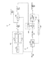
図9は、OLEDエミッターのようなELエミッターに電流を流すELサブピクセル15、及び関連回路部を示す。ELサブピクセル15は、駆動トランジスタ201と、ELエミッター202と、オプションでストレージキャパシタ1002及び選択トランジスタ36とを備える。第1の電圧供給源211(「PVDD」)は正とすることができ、第2の電圧供給源206(「Vcom」)は負とすることができる。ELエミッター202は、第1の電極207及び第2の電極208を有する。駆動トランジスタは、ゲート電極203と、駆動トランジスタのドレインすることができる第1の供給電極204と、駆動トランジスタのソースとすることができる第2の供給電極205とを有する。オプションでは選択トランジスタ36を通して、駆動トランジスタ制御信号をゲート電極203に与えることができる。駆動トランジスタ制御信号は、ストレージキャパシタ1002に格納することができる。第1の供給電極204は、第1の電圧供給源211に電気的に接続される。第2の供給電極205は、ELエミッターに電流を流すために、ELエミッター202の第1の電極207に電気的に接続される。ELエミッターの第2の電極208は、第2の電圧供給源206に電気的に接続される。電圧供給源は通常ELパネル外に配置される。電気的接続は、スイッチ、バス線、導通トランジスタ、又は電流のための経路を提供することができる他のデバイス若しくは構造を通して行なうことができる。
ハードウエア
さらに図2を参照すると、パネル上にあるどの特殊な電子回路にも頼ることなく、ELサブピクセル15の電流を測定するために、本発明は、電流ミラーユニット210、相関ダブルサンプリング(CDS)ユニット220、並びにオプションでアナログ/デジタルコンバータ(ADC)230及びステータス信号生成ユニット240を含む測定用回路16を用いる。
電流ミラーユニット210によって、単一の時点におけるELサブピクセルのための電流を測定できるようになる。信号対雑音比を改善するために、一実施形態において、本発明は相関ダブルサンプリングを用いる。
実際には、電流波形はきれいなステップではない可能性があるので、波形が整定するのを待った後にのみ測定を行なうことができる。各サブピクセルを何度も測定し、合わせてその平均をとることもできる。そのような測定は、連続して、又は別々の測定パスにおいて行なうことができる。電圧供給源206と211との間のキャパシタンスは、整定時間に加算することができる。このキャパシタンスは、通常の動作において一般的であるように、パネルに内在するか、外部キャパシタによって与えることができる。測定を行なう間に外部キャパシタを電気的に切断するために用いることができるスイッチを設けることが有利となる場合がある。
これまでの検討では、一旦、サブピクセルがオンになり、或る電流に整定すると、その列の残りの部分に対してその電流のままであると仮定する。その仮定を破る可能性がある2つの作用が、ストレージキャパシタ漏れ及びサブピクセル内作用である。
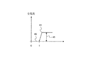
図4Aを参照すると、I−V曲線501は、経時変化前のサブピクセルの測定された特性である。I−V曲線502は、経時変化後のサブピクセルの測定された特性である。曲線501、及び502は、異なる電流レベルにおける同一の電圧差503、504、505、及び506によって示されるように、主に水平方向のシフトによって分離される。すなわち、経時変化の主な作用は、ゲート電圧軸上で一定の量だけI−V曲線をシフトすることである。これは、MOSFET飽和領域の駆動トランジスタの式、Id=K(Vgs−Vth)2に従う(Lurch, N. Fundamentals of electronics, 2e. New York: John Wiley & Sons, 1971, pg. 110):駆動トランジスタが動作すると、Vthは増加し、そして、Vthが増加すると、それに応じてVgsが増加して、Idを一定に保持する。それゆえ、Vgsを一定にする結果として、Vthが増加すると、Idsが小さくなる。
Ids=K[2(Vgs−Vth)Vds−Vds 2]
であり(Lurch, op. cit., pg. 112)、電流IdsはVdsに大きく依存する。図9に示されるように、
Vds=(PVDD−Vcom)−Voled
であるので、線形領域におけるIdsはVoledに大きく依存する。それゆえ、駆動トランジスタ201の線形動作領域において電流を測定することは、飽和領域において同じ測定を行なうのに比べて、新品のOLEDエミッター(511)と経時変化したOLEDエミッター(512a)との間の測定電流の変化の大きさを大きくするので好都合である。
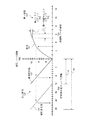
図5Aを参照すると、補償器13の一実施形態が示される。補償器13への入力は線形コード値602であり、それは、ELサブピクセル15のための指示される駆動電圧を表すことができる。補償器13は、その線形コード値を変更して、ソースドライバのための変更済み線形コード値を生成し、それは、たとえば、補償済み電圧出力603とすることができる。補償器13は、4つの主なブロック:サブピクセルの製造後経過時間を求める(61)、オプションでOLED効率を補償する(62)、製造後経過時間に基づいて補償を決定する(63)及び補償する(64)を含むことができる。ブロック61及び62は主にOLED効率補償に関連し、ブロック63及び64は主に電圧補償、具体的には、Vth/Voled補償に関連する。
Vout=Vin+ΔVth(1+α(Vg,ref−Vin)) (式1)
ただし、Voutは、補償済み電圧出力603であり、ΔVthは電圧シフト631であり、αはアルファ値632であり、Vg,refは測定基準ゲート電圧510であり、Vinは効率的な調整済み電圧622である。補償済み電圧出力は、ソースドライバのための変更済み線形コード値として表すことができ、駆動トランジスタ及びELエミッターの或る期間にわたる動作によって引き起こされる駆動トランジスタ及びELエミッターの特性の変動を補償する。
当該技術分野において既知の画像処理経路は通常非線形コード値(NLCV)、すなわち、輝度に対して非線形の関係を有するデジタル値を生成する(Giorgianni & Madden著「Digital Color Management: encoding solutions」(Reading, Mass.: Addison-Wesley, 1998. Ch. 13, pp. 283-295))。非線形出力を用いることは、通常のソースドライバの入力領域に一致し、かつコード値精度範囲を人の目の精度範囲に一致させる。しかしながら、Vthシフトは電圧領域動作であるので、線形電圧空間において実施されることが好ましい。ソースドライバを使用し、ソースドライバの前に領域変換を実行して、非線形領域画像処理経路を線形領域補償器と実効的に統合することができる。この検討はデジタル処理に関するものであるが、アナログ又はデジタル/アナログ混在システムにおいても同様の処理を実行できることに留意されたい。また、補償器は、電圧以外の線形空間において動作できることにも留意されたい。たとえば、補償器は線形電流空間において動作することができる。
パネル設計特徴付け
このセクションは、特定のOLEDパネル設計の大量生産との関連で説明される。大量生産を開始する前に、その設計を特徴付けることができる。加速寿命試験を実行することができ、種々のレベルまで経時変化した種々のサンプル基板上の種々の色の種々のサブピクセルに対してI−V曲線を測定することができる。必要とされる測定の数及びタイプ、並びに経時変化レベルの数及びタイプは、特定のパネルの特性による。これらの測定値を用いて、値アルファ(α)を計算することができ、測定基準ゲート電圧を選択することができる。アルファ(図5C 項632)は、経時的な直線シフトからの偏差を表す値である。0のα値は、たとえば、Vthシフトのみの場合に当てはまるように、全ての経時変化が電圧軸上で直線的なシフトであることを示す。測定基準ゲート電圧(図4A 510)は、補償のために経時変化信号測定が行なわれる電圧であり、許容可能なS/N比を与えつつ、かつ電力損を低く抑えるように選択することができる。

設計が特徴付けられると、大量生産を開始することができる。製造時に、ステータス信号生成ユニット240の選択された実施形態に従って、生産されるサブピクセル毎に適切な値が測定される。たとえば、I−V曲線及びサブピクセル電流を測定することができる。現実的なI−V曲線を形成するだけの十分な駆動電圧において電流を測定することができ、I−V曲線における任意の誤差が結果に影響を及ぼす可能性がある。測定基準ゲート電圧においてサブピクセル電流を測定して、ターゲット信号i0611を与えることができる。I−V曲線及び基準電流は、サブピクセルに関連付けられる不揮発性メモリに格納され、現場に送られる。
現場に出ると、サブピクセルは、如何に激しく駆動されるかによって決まる速度で経時変化する。しばらくして、サブピクセルが、補償される必要があるほど十分にシフトした。その時点を判断する方法が、以下において検討される。
11 非線形入力信号
12 線形領域へのコンバータ
13 補償器
14 ソースドライバ
15 ELサブピクセル
16 電流測定回路
32 列線
34 ゲート線
36 選択トランジスタ
41 電流
43 差
49 電流
61 ブロック
62 ブロック
63 ブロック
64 ブロック
78 電圧範囲
79 電圧範囲
90 直線の当てはめ
127 象限
137 象限
200 スイッチ
201 駆動トランジスタ
202 ELエミッター
203 ゲート電極
204 第1の供給電極
205 第2の供給電極
206 電圧供給源
207 第1の電極
208 第2の電極
210 電流ミラーユニット
211 電圧供給源
212 第1の電流ミラー
213 第1の電流ミラー出力
214 第2の電流ミラー
215 バイアス供給源
216 電流/電圧コンバータ
220 相関ダブルサンプリングユニット
221 サンプルアンドホールドユニット
222 サンプルアンドホールドユニット
223 差動増幅器
230 アナログ/デジタルコンバータ
240 ステータス信号生成ユニット
501 経時変化していないI−V曲線
502 経時変化したI−V曲線
503 電圧差
504 電圧差
505 電圧差
506 電圧差
510 測定基準ゲート電圧
511 電流
512a 電流
512b 電流
513 電圧
514 電圧シフト
550 電圧シフト
552 電圧シフト
602 線形コード値
603 補償済み電圧
611 電流
612 電流
613 パーセント電流
614 パーセント効率
615 むら補正利得項
616 むら補償オフセット項
619 メモリ
621 電流
622 電圧
626 ブロック
628 演算
631 電圧シフト
632 アルファ値
633 演算
691 I−V曲線
692 I−V曲線の反転
695 モデル
701 軸
702 軸
703 軸
711 変換における最小の変化
712 ステップ
713 ステップ
721 変換
722 変換
1002 ストレージキャパシタ
1011 バス線
1012 シートカソード
Claims (9)
- 第1の電極及び第2の電極を備えるエレクトロルミネッセント(EL)エミッターを有し、かつ第1の供給電極、第2の供給電極及びゲート電極を備える駆動トランジスタを備えるエレクトロルミネッセント(EL)サブピクセルであって、前記駆動トランジスタの前記第2の供給電極は、前記ELエミッターに電流を流すために、該ELエミッターの前記第1の電極に電気的に接続される、エレクトロルミネッセントサブピクセルと、
前記駆動トランジスタの前記第1の供給電極に電気的に接続される第1の電圧供給源と、
前記ELエミッターの前記第2の電極に電気的に接続される第2の電圧供給源と、
前記駆動トランジスタの前記ゲート電極に電気的に接続される試験電圧源と、
前記第1の電圧供給源、前記第2の電圧供給源及び前記試験電圧源の電圧を制御し、前記駆動トランジスタを線形領域において動作させるための電圧コントローラーと、
種々の時点において前記駆動トランジスタの前記第1の供給電極及び前記第2の供給電極を通って流れる電流を測定し、前記駆動トランジスタ及び前記ELエミッターの或る期間にわたる動作によって引き起こされる該駆動トランジスタ及び該ELエミッターの特性の変動を表すステータス信号を与えるための測定回路であって、前記電流は、前記駆動トランジスタが前記線形領域において動作している間に測定される、測定回路と、
線形コード値を与える手段と、
前記ステータス信号に応答して前記線形コード値を変更し、前記駆動トランジスタ及び前記ELエミッターの特性の変動を補償するための補償器と、
前記駆動トランジスタの前記ゲート電極を駆動するために、変更済み線形コード値に応答して駆動トランジスタ制御信号を生成するためのソースドライバと、
を備え、前記ELサブピクセル内の前記駆動トランジスタの前記ゲート電極に前記駆動トランジスタ制御信号を与えるための装置であって、
前記測定回路は、
前記第1の供給電極及び前記第2の供給電極を通って流れる前記駆動電流の関数であるミラー電流を生成するための第1の電流ミラーと、
前記第1の電流ミラーにバイアス電流を流して該第1の電流ミラーのインピーダンスを下げるための第2の電流ミラーと
を含み、
前記駆動トランジスタの線形動作領域において、経時変化していない前記ELエミッターと経時変化した前記ELエミッターとの間の測定電流の変化を測定する、装置。 - 前記ELエミッターはOLEDエミッターからなる、請求項1に記載の装置。
- 前記駆動トランジスタは低温ポリシリコントランジスタからなる、請求項1に記載の装置。
- 前記測定回路を、前記第1の供給電極及び前記第2の供給電極を通って流れる電流に選択的に電気的に接続するためのスイッチをさらに備える、請求項1に記載の装置。
- 前記測定回路はさらに、前記ミラー電流に応答して、電圧信号を生成するための電流/電圧コンバータと、該電圧信号に応答して、前記ステータス信号を前記補償器に与える手段とを含む、請求項1に記載の装置。
- 前記駆動トランジスタ制御信号は電圧からなる、請求項1に記載の装置。
- 前記測定される電流は、前記ELエミッターから光を放射するために必要とされる電流として選択されるしきい値電流よりも小さい、請求項1に記載の装置。
- 前記測定回路は、パネル製造時に得られた、経時変化していない電流測定値であるターゲット信号及び直近の測定時に得られた経時変化した電流測定値を格納するためのメモリをさらに備える、請求項1に記載の装置。
- 前記補償器は、前記線形コード値を変更して、変更済み線形コード値を生成し、前記駆動トランジスタ及び前記ELエミッターの特性の変動を補償する、請求項1に記載の装置。
Applications Claiming Priority (3)
| Application Number | Priority Date | Filing Date | Title |
|---|---|---|---|
| US12/396,662 US8217928B2 (en) | 2009-03-03 | 2009-03-03 | Electroluminescent subpixel compensated drive signal |
| US12/396,662 | 2009-03-03 | ||
| PCT/US2010/025354 WO2010101760A1 (en) | 2009-03-03 | 2010-02-25 | Electroluminescent subpixel compensated drive signal |
Publications (3)
| Publication Number | Publication Date |
|---|---|
| JP2012519880A JP2012519880A (ja) | 2012-08-30 |
| JP2012519880A5 JP2012519880A5 (ja) | 2012-12-27 |
| JP5416228B2 true JP5416228B2 (ja) | 2014-02-12 |
Family
ID=42136035
Family Applications (1)
| Application Number | Title | Priority Date | Filing Date |
|---|---|---|---|
| JP2011552987A Active JP5416228B2 (ja) | 2009-03-03 | 2010-02-25 | エレクトロルミネッセント(el)サブピクセル内の駆動トランジスタのゲート電極に駆動トランジスタ制御信号を与えるための装置 |
Country Status (7)
| Country | Link |
|---|---|
| US (1) | US8217928B2 (ja) |
| EP (1) | EP2404292B1 (ja) |
| JP (1) | JP5416228B2 (ja) |
| KR (1) | KR101298161B1 (ja) |
| CN (1) | CN102414737B (ja) |
| TW (1) | TWI385622B (ja) |
| WO (1) | WO2010101760A1 (ja) |
Families Citing this family (91)
| Publication number | Priority date | Publication date | Assignee | Title |
|---|---|---|---|---|
| CA2443206A1 (en) | 2003-09-23 | 2005-03-23 | Ignis Innovation Inc. | Amoled display backplanes - pixel driver circuits, array architecture, and external compensation |
| CA2504571A1 (en) * | 2005-04-12 | 2006-10-12 | Ignis Innovation Inc. | A fast method for compensation of non-uniformities in oled displays |
| WO2006063448A1 (en) | 2004-12-15 | 2006-06-22 | Ignis Innovation Inc. | Method and system for programming, calibrating and driving a light emitting device display |
| US9275579B2 (en) | 2004-12-15 | 2016-03-01 | Ignis Innovation Inc. | System and methods for extraction of threshold and mobility parameters in AMOLED displays |
| US20140111567A1 (en) | 2005-04-12 | 2014-04-24 | Ignis Innovation Inc. | System and method for compensation of non-uniformities in light emitting device displays |
| US8576217B2 (en) | 2011-05-20 | 2013-11-05 | Ignis Innovation Inc. | System and methods for extraction of threshold and mobility parameters in AMOLED displays |
| US9799246B2 (en) | 2011-05-20 | 2017-10-24 | Ignis Innovation Inc. | System and methods for extraction of threshold and mobility parameters in AMOLED displays |
| US10012678B2 (en) | 2004-12-15 | 2018-07-03 | Ignis Innovation Inc. | Method and system for programming, calibrating and/or compensating, and driving an LED display |
| US9280933B2 (en) | 2004-12-15 | 2016-03-08 | Ignis Innovation Inc. | System and methods for extraction of threshold and mobility parameters in AMOLED displays |
| US10013907B2 (en) | 2004-12-15 | 2018-07-03 | Ignis Innovation Inc. | Method and system for programming, calibrating and/or compensating, and driving an LED display |
| CN102663977B (zh) | 2005-06-08 | 2015-11-18 | 伊格尼斯创新有限公司 | 用于驱动发光器件显示器的方法和系统 |
| CA2518276A1 (en) | 2005-09-13 | 2007-03-13 | Ignis Innovation Inc. | Compensation technique for luminance degradation in electro-luminance devices |
| TW200746022A (en) | 2006-04-19 | 2007-12-16 | Ignis Innovation Inc | Stable driving scheme for active matrix displays |
| CA2556961A1 (en) | 2006-08-15 | 2008-02-15 | Ignis Innovation Inc. | Oled compensation technique based on oled capacitance |
| US8358256B2 (en) * | 2008-11-17 | 2013-01-22 | Global Oled Technology Llc | Compensated drive signal for electroluminescent display |
| US8665295B2 (en) * | 2008-11-20 | 2014-03-04 | Global Oled Technology Llc | Electroluminescent display initial-nonuniformity-compensated drve signal |
| US8194063B2 (en) * | 2009-03-04 | 2012-06-05 | Global Oled Technology Llc | Electroluminescent display compensated drive signal |
| US9384698B2 (en) | 2009-11-30 | 2016-07-05 | Ignis Innovation Inc. | System and methods for aging compensation in AMOLED displays |
| US9311859B2 (en) | 2009-11-30 | 2016-04-12 | Ignis Innovation Inc. | Resetting cycle for aging compensation in AMOLED displays |
| US10319307B2 (en) | 2009-06-16 | 2019-06-11 | Ignis Innovation Inc. | Display system with compensation techniques and/or shared level resources |
| CA2669367A1 (en) | 2009-06-16 | 2010-12-16 | Ignis Innovation Inc | Compensation technique for color shift in displays |
| CA2688870A1 (en) | 2009-11-30 | 2011-05-30 | Ignis Innovation Inc. | Methode and techniques for improving display uniformity |
| US10996258B2 (en) | 2009-11-30 | 2021-05-04 | Ignis Innovation Inc. | Defect detection and correction of pixel circuits for AMOLED displays |
| US8803417B2 (en) | 2009-12-01 | 2014-08-12 | Ignis Innovation Inc. | High resolution pixel architecture |
| US9881532B2 (en) | 2010-02-04 | 2018-01-30 | Ignis Innovation Inc. | System and method for extracting correlation curves for an organic light emitting device |
| US10089921B2 (en) | 2010-02-04 | 2018-10-02 | Ignis Innovation Inc. | System and methods for extracting correlation curves for an organic light emitting device |
| CA2692097A1 (en) | 2010-02-04 | 2011-08-04 | Ignis Innovation Inc. | Extracting correlation curves for light emitting device |
| US20140313111A1 (en) | 2010-02-04 | 2014-10-23 | Ignis Innovation Inc. | System and methods for extracting correlation curves for an organic light emitting device |
| US10176736B2 (en) | 2010-02-04 | 2019-01-08 | Ignis Innovation Inc. | System and methods for extracting correlation curves for an organic light emitting device |
| US10163401B2 (en) | 2010-02-04 | 2018-12-25 | Ignis Innovation Inc. | System and methods for extracting correlation curves for an organic light emitting device |
| CA2696778A1 (en) | 2010-03-17 | 2011-09-17 | Ignis Innovation Inc. | Lifetime, uniformity, parameter extraction methods |
| EP2453433B1 (en) * | 2010-11-15 | 2018-10-10 | Ignis Innovation Inc. | System and method for compensation of non-uniformities in light emitting device displays |
| US8907991B2 (en) | 2010-12-02 | 2014-12-09 | Ignis Innovation Inc. | System and methods for thermal compensation in AMOLED displays |
| TWI433096B (zh) * | 2011-01-27 | 2014-04-01 | Novatek Microelectronics Corp | 面板驅動電路 |
| CN102637402B (zh) * | 2011-02-15 | 2014-09-10 | 联咏科技股份有限公司 | 面板驱动电路 |
| US9530349B2 (en) | 2011-05-20 | 2016-12-27 | Ignis Innovations Inc. | Charged-based compensation and parameter extraction in AMOLED displays |
| US9466240B2 (en) | 2011-05-26 | 2016-10-11 | Ignis Innovation Inc. | Adaptive feedback system for compensating for aging pixel areas with enhanced estimation speed |
| WO2012164475A2 (en) | 2011-05-27 | 2012-12-06 | Ignis Innovation Inc. | Systems and methods for aging compensation in amoled displays |
| US9324268B2 (en) | 2013-03-15 | 2016-04-26 | Ignis Innovation Inc. | Amoled displays with multiple readout circuits |
| US10089924B2 (en) | 2011-11-29 | 2018-10-02 | Ignis Innovation Inc. | Structural and low-frequency non-uniformity compensation |
| US9292025B2 (en) | 2011-12-19 | 2016-03-22 | Mediatek Singapore Pte. Ltd. | Performance, thermal and power management system associated with an integrated circuit and related method |
| US8937632B2 (en) | 2012-02-03 | 2015-01-20 | Ignis Innovation Inc. | Driving system for active-matrix displays |
| US9747834B2 (en) | 2012-05-11 | 2017-08-29 | Ignis Innovation Inc. | Pixel circuits including feedback capacitors and reset capacitors, and display systems therefore |
| US8922544B2 (en) | 2012-05-23 | 2014-12-30 | Ignis Innovation Inc. | Display systems with compensation for line propagation delay |
| US9064464B2 (en) | 2012-06-25 | 2015-06-23 | Apple Inc. | Systems and methods for calibrating a display to reduce or eliminate mura artifacts |
| US9336717B2 (en) | 2012-12-11 | 2016-05-10 | Ignis Innovation Inc. | Pixel circuits for AMOLED displays |
| US9786223B2 (en) | 2012-12-11 | 2017-10-10 | Ignis Innovation Inc. | Pixel circuits for AMOLED displays |
| KR102122517B1 (ko) * | 2012-12-17 | 2020-06-12 | 엘지디스플레이 주식회사 | 유기발광 표시장치 |
| EP3043338A1 (en) | 2013-03-14 | 2016-07-13 | Ignis Innovation Inc. | Re-interpolation with edge detection for extracting an aging pattern for amoled displays |
| WO2014174427A1 (en) | 2013-04-22 | 2014-10-30 | Ignis Innovation Inc. | Inspection system for oled display panels |
| US9697769B2 (en) * | 2013-07-30 | 2017-07-04 | Sharp Kabushiki Kaisha | Display device and drive method for same |
| CN103400548B (zh) * | 2013-07-31 | 2016-03-16 | 京东方科技集团股份有限公司 | 像素驱动电路及其驱动方法、显示装置 |
| CN107452314B (zh) | 2013-08-12 | 2021-08-24 | 伊格尼斯创新公司 | 用于要被显示器显示的图像的补偿图像数据的方法和装置 |
| KR102058577B1 (ko) | 2013-09-13 | 2019-12-24 | 삼성디스플레이 주식회사 | 표시 장치 및 그 구동 방법 |
| KR101603300B1 (ko) * | 2013-11-25 | 2016-03-14 | 엘지디스플레이 주식회사 | 유기발광표시장치 및 그 표시패널 |
| US9761170B2 (en) | 2013-12-06 | 2017-09-12 | Ignis Innovation Inc. | Correction for localized phenomena in an image array |
| US9741282B2 (en) | 2013-12-06 | 2017-08-22 | Ignis Innovation Inc. | OLED display system and method |
| US9502653B2 (en) | 2013-12-25 | 2016-11-22 | Ignis Innovation Inc. | Electrode contacts |
| US10192479B2 (en) | 2014-04-08 | 2019-01-29 | Ignis Innovation Inc. | Display system using system level resources to calculate compensation parameters for a display module in a portable device |
| US10002568B2 (en) * | 2014-05-09 | 2018-06-19 | Joled Inc. | Display unit, display unit driving method, and electronic apparatus with deterioration suppression |
| CN104021760B (zh) * | 2014-05-30 | 2016-03-02 | 京东方科技集团股份有限公司 | 一种用于oled显示器件的伽马电压的调节方法 |
| CN112002285B (zh) * | 2014-06-25 | 2021-10-29 | 伊格尼斯创新公司 | 用于确定和补偿有机发光器件的效率劣化的方法 |
| JP2016009165A (ja) * | 2014-06-26 | 2016-01-18 | ローム株式会社 | 電気光学装置、電気光学装置の特性測定方法、及び半導体チップ |
| CN104464626B (zh) * | 2014-12-12 | 2016-10-05 | 京东方科技集团股份有限公司 | 有机电致发光显示装置及方法 |
| US9728125B2 (en) * | 2014-12-22 | 2017-08-08 | Shenzhen China Star Optoelectronics Technology Co., Ltd | AMOLED pixel circuit |
| KR102219507B1 (ko) * | 2014-12-30 | 2021-02-23 | 엘지디스플레이 주식회사 | 유기발광표시장치 및 그 화질 보상 장치 및 방법 |
| US10388217B2 (en) * | 2015-01-19 | 2019-08-20 | Sharp Kabushiki Kaisha | Display device and method of driving same |
| CA2879462A1 (en) | 2015-01-23 | 2016-07-23 | Ignis Innovation Inc. | Compensation for color variation in emissive devices |
| CA2889870A1 (en) | 2015-05-04 | 2016-11-04 | Ignis Innovation Inc. | Optical feedback system |
| CA2892714A1 (en) | 2015-05-27 | 2016-11-27 | Ignis Innovation Inc | Memory bandwidth reduction in compensation system |
| CN105096824B (zh) | 2015-08-06 | 2017-08-11 | 青岛海信电器股份有限公司 | 自发光显示器灰阶补偿方法、装置和自发光显示设备 |
| CA2900170A1 (en) | 2015-08-07 | 2017-02-07 | Gholamreza Chaji | Calibration of pixel based on improved reference values |
| US10621913B2 (en) * | 2015-12-14 | 2020-04-14 | Sharp Kabushiki Kaisha | Display device and driving method therefor |
| CN106531083A (zh) * | 2016-12-15 | 2017-03-22 | 上海天马有机发光显示技术有限公司 | 像素电路的补偿方法、oled显示面板及其补偿方法 |
| WO2018212843A1 (en) * | 2017-05-15 | 2018-11-22 | Apple Inc. | Systems and methods of utilizing output of display component for display temperature compensation |
| US10943516B2 (en) | 2017-05-15 | 2021-03-09 | Apple Inc. | Systems and methods of utilizing output of display component for display temperature compensation |
| CN109671393B (zh) * | 2017-10-13 | 2020-07-31 | 京东方科技集团股份有限公司 | 一种像素补偿方法及系统、显示装置 |
| CN109671396A (zh) | 2017-10-17 | 2019-04-23 | 伊格尼斯创新公司 | 像素电路、显示装置和方法 |
| CN109697944B (zh) * | 2017-10-20 | 2020-11-24 | 京东方科技集团股份有限公司 | 像素电路的检测方法、显示面板的驱动方法和显示装置 |
| CN107705758A (zh) * | 2017-10-26 | 2018-02-16 | 惠科股份有限公司 | 显示系统及电流驱动方法 |
| US10984713B1 (en) * | 2018-05-10 | 2021-04-20 | Apple Inc. | External compensation for LTPO pixel for OLED display |
| CN109040751A (zh) * | 2018-09-21 | 2018-12-18 | 中新科技集团股份有限公司 | 一种电视老化处理的控制设备 |
| CN109256088B (zh) * | 2018-10-31 | 2021-10-01 | 京东方科技集团股份有限公司 | 像素电路、显示面板、显示装置和像素驱动方法 |
| US11373566B2 (en) * | 2018-12-18 | 2022-06-28 | Innolux Corporation | Electronic device and manufacturing process thereof |
| US11282458B2 (en) * | 2019-06-10 | 2022-03-22 | Apple Inc. | Systems and methods for temperature-based parasitic capacitance variation compensation |
| CN111354312B (zh) * | 2019-12-27 | 2021-04-27 | 深圳市华星光电半导体显示技术有限公司 | 用于显示面板中oled效率衰减补偿方法、装置及系统 |
| US11632830B2 (en) * | 2020-08-07 | 2023-04-18 | Samsung Display Co., Ltd. | System and method for transistor parameter estimation |
| CN112466767B (zh) * | 2020-11-10 | 2023-10-31 | 海光信息技术股份有限公司 | 一种集成电路的老化补偿方法、集成电路 |
| JP2022137420A (ja) | 2021-03-09 | 2022-09-22 | 信越化学工業株式会社 | ポリイミドを含む重合体、ポジ型感光性樹脂組成物、ネガ型感光性樹脂組成物、パターン形成方法、硬化被膜形成方法、層間絶縁膜、表面保護膜、及び電子部品 |
| CN113112961A (zh) * | 2021-04-12 | 2021-07-13 | 深圳市华星光电半导体显示技术有限公司 | 显示驱动电路及显示驱动电路的驱动方法 |
| TWI786911B (zh) * | 2021-10-29 | 2022-12-11 | 友達光電股份有限公司 | 顯示裝置、校正方法及畫面顯示方法 |
Family Cites Families (24)
| Publication number | Priority date | Publication date | Assignee | Title |
|---|---|---|---|---|
| EP0264667B1 (de) | 1986-10-24 | 1992-12-02 | F. Hoffmann-La Roche Ag | Flüssigkristallanzeigezelle |
| JPH01217421A (ja) | 1988-02-26 | 1989-08-31 | Seikosha Co Ltd | 非晶質シリコン薄膜トランジスタアレイ基板およびその製造方法 |
| US6518962B2 (en) | 1997-03-12 | 2003-02-11 | Seiko Epson Corporation | Pixel circuit display apparatus and electronic apparatus equipped with current driving type light-emitting device |
| GB0014961D0 (en) | 2000-06-20 | 2000-08-09 | Koninkl Philips Electronics Nv | Light-emitting matrix array display devices with light sensing elements |
| TW569016B (en) * | 2001-01-29 | 2004-01-01 | Semiconductor Energy Lab | Light emitting device |
| JP2002229513A (ja) * | 2001-02-06 | 2002-08-16 | Tohoku Pioneer Corp | 有機el表示パネルの駆動装置 |
| TWI221268B (en) * | 2001-09-07 | 2004-09-21 | Semiconductor Energy Lab | Light emitting device and method of driving the same |
| JP2003195813A (ja) * | 2001-09-07 | 2003-07-09 | Semiconductor Energy Lab Co Ltd | 発光装置 |
| JP4655457B2 (ja) * | 2003-08-08 | 2011-03-23 | 富士ゼロックス株式会社 | 光量制御装置及びこれを用いた画像形成装置 |
| JP4649824B2 (ja) * | 2003-08-15 | 2011-03-16 | 富士ゼロックス株式会社 | 光量制御装置及び画像形成装置 |
| JP3628014B1 (ja) | 2003-09-19 | 2005-03-09 | ウインテスト株式会社 | 表示装置及びそれに用いるアクティブマトリクス基板の検査方法及び装置 |
| JP4804711B2 (ja) * | 2003-11-21 | 2011-11-02 | 株式会社 日立ディスプレイズ | 画像表示装置 |
| US6995519B2 (en) | 2003-11-25 | 2006-02-07 | Eastman Kodak Company | OLED display with aging compensation |
| DE102004022424A1 (de) * | 2004-05-06 | 2005-12-01 | Deutsche Thomson-Brandt Gmbh | Schaltung und Ansteuerverfahren für eine Leuchtanzeige |
| DE102004045871B4 (de) | 2004-09-20 | 2006-11-23 | Novaled Gmbh | Verfahren und Schaltungsanordnung zur Alterungskompensation von organischen Lichtemitterdioden |
| US7116058B2 (en) | 2004-11-30 | 2006-10-03 | Wintek Corporation | Method of improving the stability of active matrix OLED displays driven by amorphous silicon thin-film transistors |
| CA2504571A1 (en) | 2005-04-12 | 2006-10-12 | Ignis Innovation Inc. | A fast method for compensation of non-uniformities in oled displays |
| EP2458579B1 (en) * | 2006-01-09 | 2017-09-20 | Ignis Innovation Inc. | Method and system for driving an active matrix display circuit |
| JP2007235627A (ja) * | 2006-03-01 | 2007-09-13 | Nippon Telegr & Teleph Corp <Ntt> | 光電流モニタ回路 |
| US20080048951A1 (en) | 2006-04-13 | 2008-02-28 | Naugler Walter E Jr | Method and apparatus for managing and uniformly maintaining pixel circuitry in a flat panel display |
| US7928936B2 (en) * | 2006-11-28 | 2011-04-19 | Global Oled Technology Llc | Active matrix display compensating method |
| JP2008250069A (ja) | 2007-03-30 | 2008-10-16 | Sanyo Electric Co Ltd | エレクトロルミネッセンス表示装置 |
| US8026873B2 (en) * | 2007-12-21 | 2011-09-27 | Global Oled Technology Llc | Electroluminescent display compensated analog transistor drive signal |
| US8665295B2 (en) * | 2008-11-20 | 2014-03-04 | Global Oled Technology Llc | Electroluminescent display initial-nonuniformity-compensated drve signal |
-
2009
- 2009-03-03 US US12/396,662 patent/US8217928B2/en active Active
-
2010
- 2010-02-25 CN CN201080019631.8A patent/CN102414737B/zh active Active
- 2010-02-25 JP JP2011552987A patent/JP5416228B2/ja active Active
- 2010-02-25 KR KR1020117023071A patent/KR101298161B1/ko active IP Right Grant
- 2010-02-25 WO PCT/US2010/025354 patent/WO2010101760A1/en active Application Filing
- 2010-02-25 EP EP10706863.7A patent/EP2404292B1/en active Active
- 2010-03-02 TW TW099106032A patent/TWI385622B/zh active
Also Published As
| Publication number | Publication date |
|---|---|
| CN102414737B (zh) | 2014-04-23 |
| TW201037667A (en) | 2010-10-16 |
| CN102414737A (zh) | 2012-04-11 |
| TWI385622B (zh) | 2013-02-11 |
| KR20110123278A (ko) | 2011-11-14 |
| US20100225630A1 (en) | 2010-09-09 |
| EP2404292B1 (en) | 2018-06-20 |
| WO2010101760A1 (en) | 2010-09-10 |
| US8217928B2 (en) | 2012-07-10 |
| KR101298161B1 (ko) | 2013-08-21 |
| EP2404292A1 (en) | 2012-01-11 |
| JP2012519880A (ja) | 2012-08-30 |
Similar Documents
| Publication | Publication Date | Title |
|---|---|---|
| JP5416228B2 (ja) | エレクトロルミネッセント(el)サブピクセル内の駆動トランジスタのゲート電極に駆動トランジスタ制御信号を与えるための装置 | |
| JP5416229B2 (ja) | エレクトロルミネッセントディスプレイ補償済み駆動信号 | |
| TWI383356B (zh) | 電場發光顯示器補償式類比電晶體驅動訊號 | |
| TWI420463B (zh) | 顯示驅動裝置及顯示裝置 | |
| JP5146521B2 (ja) | 画素駆動装置、発光装置及びその駆動制御方法、並びに、電子機器 | |
| US8059070B2 (en) | Display device, and methods for manufacturing and controlling the display device | |
| JP5466243B2 (ja) | Elサブピクセル内の駆動トランジスタのゲート電極にアナログ駆動トランジスタ制御信号を与えるための装置 | |
| KR101325978B1 (ko) | 유기전계 발광 디스플레이 장치용 구동회로 | |
| JP2011138036A (ja) | 画素駆動装置、発光装置及びその駆動制御方法、並びに、電子機器 | |
| US20070290947A1 (en) | Method and apparatus for compensating aging of an electroluminescent display | |
| JP2015106096A (ja) | 表示装置及びその補償データ算出方法及びその駆動方法 | |
| CN114902319A (zh) | 显示装置及操作显示装置的方法 |
Legal Events
| Date | Code | Title | Description |
|---|---|---|---|
| A521 | Request for written amendment filed |
Free format text: JAPANESE INTERMEDIATE CODE: A523 Effective date: 20121108 |
|
| A621 | Written request for application examination |
Free format text: JAPANESE INTERMEDIATE CODE: A621 Effective date: 20121108 |
|
| A871 | Explanation of circumstances concerning accelerated examination |
Free format text: JAPANESE INTERMEDIATE CODE: A871 Effective date: 20121108 |
|
| A975 | Report on accelerated examination |
Free format text: JAPANESE INTERMEDIATE CODE: A971005 Effective date: 20130208 |
|
| A131 | Notification of reasons for refusal |
Free format text: JAPANESE INTERMEDIATE CODE: A131 Effective date: 20130219 |
|
| A521 | Request for written amendment filed |
Free format text: JAPANESE INTERMEDIATE CODE: A523 Effective date: 20130514 |
|
| A131 | Notification of reasons for refusal |
Free format text: JAPANESE INTERMEDIATE CODE: A131 Effective date: 20130820 |
|
| A521 | Request for written amendment filed |
Free format text: JAPANESE INTERMEDIATE CODE: A523 Effective date: 20131009 |
|
| TRDD | Decision of grant or rejection written | ||
| A01 | Written decision to grant a patent or to grant a registration (utility model) |
Free format text: JAPANESE INTERMEDIATE CODE: A01 Effective date: 20131112 |
|
| A61 | First payment of annual fees (during grant procedure) |
Free format text: JAPANESE INTERMEDIATE CODE: A61 Effective date: 20131114 |
|
| R150 | Certificate of patent or registration of utility model |
Ref document number: 5416228 Country of ref document: JP Free format text: JAPANESE INTERMEDIATE CODE: R150 |
|
| R250 | Receipt of annual fees |
Free format text: JAPANESE INTERMEDIATE CODE: R250 |
|
| R250 | Receipt of annual fees |
Free format text: JAPANESE INTERMEDIATE CODE: R250 |
|
| R250 | Receipt of annual fees |
Free format text: JAPANESE INTERMEDIATE CODE: R250 |
|
| R250 | Receipt of annual fees |
Free format text: JAPANESE INTERMEDIATE CODE: R250 |
|
| R250 | Receipt of annual fees |
Free format text: JAPANESE INTERMEDIATE CODE: R250 |
|
| R250 | Receipt of annual fees |
Free format text: JAPANESE INTERMEDIATE CODE: R250 |
|
| R250 | Receipt of annual fees |
Free format text: JAPANESE INTERMEDIATE CODE: R250 |
|
| R250 | Receipt of annual fees |
Free format text: JAPANESE INTERMEDIATE CODE: R250 |