JP5416228B2 - Apparatus for providing a drive transistor control signal to a gate electrode of a drive transistor in an electroluminescent (EL) subpixel - Google Patents
Apparatus for providing a drive transistor control signal to a gate electrode of a drive transistor in an electroluminescent (EL) subpixel Download PDFInfo
- Publication number
- JP5416228B2 JP5416228B2 JP2011552987A JP2011552987A JP5416228B2 JP 5416228 B2 JP5416228 B2 JP 5416228B2 JP 2011552987 A JP2011552987 A JP 2011552987A JP 2011552987 A JP2011552987 A JP 2011552987A JP 5416228 B2 JP5416228 B2 JP 5416228B2
- Authority
- JP
- Japan
- Prior art keywords
- current
- voltage
- drive transistor
- emitter
- subpixel
- Prior art date
- Legal status (The legal status is an assumption and is not a legal conclusion. Google has not performed a legal analysis and makes no representation as to the accuracy of the status listed.)
- Active
Links
- 238000005259 measurement Methods 0.000 claims description 118
- 230000008859 change Effects 0.000 claims description 24
- 230000006870 function Effects 0.000 claims description 18
- 238000004519 manufacturing process Methods 0.000 claims description 18
- 230000004044 response Effects 0.000 claims description 11
- 238000012360 testing method Methods 0.000 claims description 11
- 229910021420 polycrystalline silicon Inorganic materials 0.000 claims description 3
- 229920005591 polysilicon Polymers 0.000 claims description 3
- 238000000034 method Methods 0.000 description 31
- 238000006243 chemical reaction Methods 0.000 description 17
- 230000000694 effects Effects 0.000 description 15
- 238000012545 processing Methods 0.000 description 15
- 229910021417 amorphous silicon Inorganic materials 0.000 description 13
- 238000013461 design Methods 0.000 description 13
- 239000003990 capacitor Substances 0.000 description 12
- 230000015556 catabolic process Effects 0.000 description 11
- 238000006731 degradation reaction Methods 0.000 description 11
- 238000003860 storage Methods 0.000 description 10
- 230000032683 aging Effects 0.000 description 9
- 238000010586 diagram Methods 0.000 description 9
- 230000007274 generation of a signal involved in cell-cell signaling Effects 0.000 description 9
- 230000002441 reversible effect Effects 0.000 description 9
- 230000007423 decrease Effects 0.000 description 8
- 238000010438 heat treatment Methods 0.000 description 8
- 239000000523 sample Substances 0.000 description 8
- 238000012512 characterization method Methods 0.000 description 7
- 238000005516 engineering process Methods 0.000 description 7
- 230000000875 corresponding effect Effects 0.000 description 6
- 239000011159 matrix material Substances 0.000 description 6
- 238000005070 sampling Methods 0.000 description 6
- 230000009466 transformation Effects 0.000 description 5
- 230000003679 aging effect Effects 0.000 description 4
- 230000009471 action Effects 0.000 description 3
- 230000002596 correlated effect Effects 0.000 description 3
- 230000008569 process Effects 0.000 description 3
- 241001487991 Lettuce chlorosis virus Species 0.000 description 2
- XLOMVQKBTHCTTD-UHFFFAOYSA-N Zinc monoxide Chemical compound [Zn]=O XLOMVQKBTHCTTD-UHFFFAOYSA-N 0.000 description 2
- 230000006399 behavior Effects 0.000 description 2
- 239000003086 colorant Substances 0.000 description 2
- 230000001276 controlling effect Effects 0.000 description 2
- 238000012937 correction Methods 0.000 description 2
- 230000007613 environmental effect Effects 0.000 description 2
- 239000000463 material Substances 0.000 description 2
- 230000003287 optical effect Effects 0.000 description 2
- 239000000758 substrate Substances 0.000 description 2
- 239000010409 thin film Substances 0.000 description 2
- 229920001621 AMOLED Polymers 0.000 description 1
- 241000959671 Chenopodium leaf curl virus Species 0.000 description 1
- UNPLRYRWJLTVAE-UHFFFAOYSA-N Cloperastine hydrochloride Chemical compound Cl.C1=CC(Cl)=CC=C1C(C=1C=CC=CC=1)OCCN1CCCCC1 UNPLRYRWJLTVAE-UHFFFAOYSA-N 0.000 description 1
- 241000023320 Luma <angiosperm> Species 0.000 description 1
- 238000013459 approach Methods 0.000 description 1
- 230000008901 benefit Effects 0.000 description 1
- 238000004364 calculation method Methods 0.000 description 1
- 238000004891 communication Methods 0.000 description 1
- 238000013480 data collection Methods 0.000 description 1
- 230000002431 foraging effect Effects 0.000 description 1
- 238000009499 grossing Methods 0.000 description 1
- 230000006872 improvement Effects 0.000 description 1
- 239000004615 ingredient Substances 0.000 description 1
- 238000012886 linear function Methods 0.000 description 1
- 238000013507 mapping Methods 0.000 description 1
- 230000008078 mathematical effect Effects 0.000 description 1
- 230000007246 mechanism Effects 0.000 description 1
- OSWPMRLSEDHDFF-UHFFFAOYSA-N methyl salicylate Chemical compound COC(=O)C1=CC=CC=C1O OSWPMRLSEDHDFF-UHFFFAOYSA-N 0.000 description 1
- 238000012986 modification Methods 0.000 description 1
- 230000004048 modification Effects 0.000 description 1
- 238000005457 optimization Methods 0.000 description 1
- 230000003071 parasitic effect Effects 0.000 description 1
- 229920000642 polymer Polymers 0.000 description 1
- 230000009290 primary effect Effects 0.000 description 1
- 239000002096 quantum dot Substances 0.000 description 1
- 230000009291 secondary effect Effects 0.000 description 1
- 239000004065 semiconductor Substances 0.000 description 1
- 230000035945 sensitivity Effects 0.000 description 1
- 150000003384 small molecules Chemical class 0.000 description 1
- 230000002123 temporal effect Effects 0.000 description 1
- 230000009293 tertiary effect Effects 0.000 description 1
- 230000036962 time dependent Effects 0.000 description 1
- 238000000844 transformation Methods 0.000 description 1
- 230000001052 transient effect Effects 0.000 description 1
- 239000011787 zinc oxide Substances 0.000 description 1
Images


Classifications
-
- G—PHYSICS
- G09—EDUCATION; CRYPTOGRAPHY; DISPLAY; ADVERTISING; SEALS
- G09G—ARRANGEMENTS OR CIRCUITS FOR CONTROL OF INDICATING DEVICES USING STATIC MEANS TO PRESENT VARIABLE INFORMATION
- G09G3/00—Control arrangements or circuits, of interest only in connection with visual indicators other than cathode-ray tubes
- G09G3/20—Control arrangements or circuits, of interest only in connection with visual indicators other than cathode-ray tubes for presentation of an assembly of a number of characters, e.g. a page, by composing the assembly by combination of individual elements arranged in a matrix no fixed position being assigned to or needed to be assigned to the individual characters or partial characters
- G09G3/22—Control arrangements or circuits, of interest only in connection with visual indicators other than cathode-ray tubes for presentation of an assembly of a number of characters, e.g. a page, by composing the assembly by combination of individual elements arranged in a matrix no fixed position being assigned to or needed to be assigned to the individual characters or partial characters using controlled light sources
- G09G3/30—Control arrangements or circuits, of interest only in connection with visual indicators other than cathode-ray tubes for presentation of an assembly of a number of characters, e.g. a page, by composing the assembly by combination of individual elements arranged in a matrix no fixed position being assigned to or needed to be assigned to the individual characters or partial characters using controlled light sources using electroluminescent panels
- G09G3/32—Control arrangements or circuits, of interest only in connection with visual indicators other than cathode-ray tubes for presentation of an assembly of a number of characters, e.g. a page, by composing the assembly by combination of individual elements arranged in a matrix no fixed position being assigned to or needed to be assigned to the individual characters or partial characters using controlled light sources using electroluminescent panels semiconductive, e.g. using light-emitting diodes [LED]
- G09G3/3208—Control arrangements or circuits, of interest only in connection with visual indicators other than cathode-ray tubes for presentation of an assembly of a number of characters, e.g. a page, by composing the assembly by combination of individual elements arranged in a matrix no fixed position being assigned to or needed to be assigned to the individual characters or partial characters using controlled light sources using electroluminescent panels semiconductive, e.g. using light-emitting diodes [LED] organic, e.g. using organic light-emitting diodes [OLED]
- G09G3/3225—Control arrangements or circuits, of interest only in connection with visual indicators other than cathode-ray tubes for presentation of an assembly of a number of characters, e.g. a page, by composing the assembly by combination of individual elements arranged in a matrix no fixed position being assigned to or needed to be assigned to the individual characters or partial characters using controlled light sources using electroluminescent panels semiconductive, e.g. using light-emitting diodes [LED] organic, e.g. using organic light-emitting diodes [OLED] using an active matrix
- G09G3/3233—Control arrangements or circuits, of interest only in connection with visual indicators other than cathode-ray tubes for presentation of an assembly of a number of characters, e.g. a page, by composing the assembly by combination of individual elements arranged in a matrix no fixed position being assigned to or needed to be assigned to the individual characters or partial characters using controlled light sources using electroluminescent panels semiconductive, e.g. using light-emitting diodes [LED] organic, e.g. using organic light-emitting diodes [OLED] using an active matrix with pixel circuitry controlling the current through the light-emitting element
-
- G—PHYSICS
- G09—EDUCATION; CRYPTOGRAPHY; DISPLAY; ADVERTISING; SEALS
- G09G—ARRANGEMENTS OR CIRCUITS FOR CONTROL OF INDICATING DEVICES USING STATIC MEANS TO PRESENT VARIABLE INFORMATION
- G09G2300/00—Aspects of the constitution of display devices
- G09G2300/08—Active matrix structure, i.e. with use of active elements, inclusive of non-linear two terminal elements, in the pixels together with light emitting or modulating elements
- G09G2300/0809—Several active elements per pixel in active matrix panels
- G09G2300/0842—Several active elements per pixel in active matrix panels forming a memory circuit, e.g. a dynamic memory with one capacitor
-
- G—PHYSICS
- G09—EDUCATION; CRYPTOGRAPHY; DISPLAY; ADVERTISING; SEALS
- G09G—ARRANGEMENTS OR CIRCUITS FOR CONTROL OF INDICATING DEVICES USING STATIC MEANS TO PRESENT VARIABLE INFORMATION
- G09G2320/00—Control of display operating conditions
- G09G2320/02—Improving the quality of display appearance
- G09G2320/0233—Improving the luminance or brightness uniformity across the screen
-
- G—PHYSICS
- G09—EDUCATION; CRYPTOGRAPHY; DISPLAY; ADVERTISING; SEALS
- G09G—ARRANGEMENTS OR CIRCUITS FOR CONTROL OF INDICATING DEVICES USING STATIC MEANS TO PRESENT VARIABLE INFORMATION
- G09G2320/00—Control of display operating conditions
- G09G2320/02—Improving the quality of display appearance
- G09G2320/029—Improving the quality of display appearance by monitoring one or more pixels in the display panel, e.g. by monitoring a fixed reference pixel
- G09G2320/0295—Improving the quality of display appearance by monitoring one or more pixels in the display panel, e.g. by monitoring a fixed reference pixel by monitoring each display pixel
-
- G—PHYSICS
- G09—EDUCATION; CRYPTOGRAPHY; DISPLAY; ADVERTISING; SEALS
- G09G—ARRANGEMENTS OR CIRCUITS FOR CONTROL OF INDICATING DEVICES USING STATIC MEANS TO PRESENT VARIABLE INFORMATION
- G09G2320/00—Control of display operating conditions
- G09G2320/04—Maintaining the quality of display appearance
- G09G2320/043—Preventing or counteracting the effects of ageing
- G09G2320/045—Compensation of drifts in the characteristics of light emitting or modulating elements
-
- G—PHYSICS
- G09—EDUCATION; CRYPTOGRAPHY; DISPLAY; ADVERTISING; SEALS
- G09G—ARRANGEMENTS OR CIRCUITS FOR CONTROL OF INDICATING DEVICES USING STATIC MEANS TO PRESENT VARIABLE INFORMATION
- G09G2360/00—Aspects of the architecture of display systems
- G09G2360/16—Calculation or use of calculated indices related to luminance levels in display data
Description
本発明はエレクトロルミネッセントエミッターを通って流れる電流を供給するための駆動トランジスタに加えられる信号の制御に関する。 The present invention relates to the control of a signal applied to a drive transistor for supplying a current flowing through an electroluminescent emitter.
コンピューティング、エンターテイメント及び通信のための情報ディスプレイとして、フラットパネルディスプレイへの関心は高い。たとえば、エレクトロルミネッセント(EL)エミッターは何年にもわたって知られており、最近になって市販のディスプレイデバイスにおいて用いられるようになった。そのようなディスプレイは、アクティブマトリックス制御方式及びパッシブマトリックス制御方式の両方を利用し、複数のサブピクセルを利用することができる。各サブピクセルは、ELエミッターと、ELエミッターを流れる電流を駆動するための駆動トランジスタとを含む。サブピクセルは通常2次元のアレイに配列され、サブピクセル毎に1つの行アドレス及び列アドレスがあり、サブピクセルにはデータ値が関連付けられる。単一ELサブピクセルを照明及びユーザーインターフェースの用途に用いることもできる。ELサブピクセルは、コーティング可能な無機発光ダイオード、量子ドット、及び有機発光ダイオード(OLED)を含む、種々のエミッター技術を用いて作製することができる。 There is a great interest in flat panel displays as information displays for computing, entertainment and communications. For example, electroluminescent (EL) emitters have been known for many years and have recently been used in commercial display devices. Such a display utilizes both an active matrix control scheme and a passive matrix control scheme and can utilize multiple subpixels. Each subpixel includes an EL emitter and a driving transistor for driving a current flowing through the EL emitter. The subpixels are typically arranged in a two-dimensional array, with one row address and column address for each subpixel, and a data value is associated with the subpixel. A single EL subpixel can also be used for lighting and user interface applications. EL subpixels can be made using a variety of emitter technologies, including coatable inorganic light emitting diodes, quantum dots, and organic light emitting diodes (OLEDs).
有機発光ダイオード(OLED)技術のようなエレクトロルミネッセント(EL)技術は、白熱ランプ及び蛍光灯のような他の技術よりもルミナンス及び消費電力に関して優れた利点を提供する。しかしながら、ELサブピクセルは経時的に性能が劣化するという難点がある。サブピクセルの寿命にわたって高品質の光放射を提供するために、この劣化を補償しなければならない。 Electroluminescent (EL) technology such as organic light emitting diode (OLED) technology offers superior advantages in terms of luminance and power consumption over other technologies such as incandescent lamps and fluorescent lamps. However, the EL subpixel has a drawback that its performance deteriorates with time. This degradation must be compensated to provide high quality light emission over the lifetime of the subpixel.
ELエミッターの光出力はエミッターを流れる電流に概ね比例するので、ELサブピクセル内の駆動トランジスタは通常、ゲート−ソース間電圧Vgsに応答する電圧制御式の電流源として構成される。LCDディスプレイにおいて用いられるソースドライバに類似のソースドライバが、駆動トランジスタに制御電圧を与える。ソースドライバは、所望のコード値をアナログ電圧に変換し、駆動トランジスタを制御することができる。より高いビット深度を有する線形ソースドライバが入手可能になりつつあるが、コード値と電圧との間の関係は通常非線形である。非線形のコード値−電圧関係は、OLEDの場合、特徴的なLCD S形状(たとえば、米国特許第4,896,947号において示される)とは異なる形状を有するが、要求されるソースドライバ電子回路は、2つの技術間で非常によく似ている。LCDソースドライバとELソースドライバとの間の類似性に加えて、米国特許第5,034,340号においてTanaka他によって教示されるように、LCDディスプレイ及びELディスプレイは通常同じ基板、すなわちアモルファスシリコン(a−Si)上に製造される。アモルファスSiは安価であり、大きなディスプレイに加工するのが容易である。 Since the light output of the EL emitter is roughly proportional to the current flowing through the emitter, the drive transistor in the EL subpixel is typically configured as a voltage controlled current source responsive to the gate-source voltage V gs . A source driver similar to that used in LCD displays provides a control voltage to the drive transistor. The source driver can convert a desired code value into an analog voltage and control the driving transistor. Although linear source drivers with higher bit depth are becoming available, the relationship between code value and voltage is usually non-linear. The non-linear code value-voltage relationship has a shape different from the characteristic LCD S shape (eg, shown in US Pat. No. 4,896,947) for OLEDs, but the required source driver electronics Are very similar between the two technologies. In addition to the similarity between LCD and EL source drivers, as taught by Tanaka et al. In US Pat. No. 5,034,340, LCD and EL displays are usually the same substrate, namely amorphous silicon ( a-Si). Amorphous Si is inexpensive and easy to process into a large display.
劣化モード
しかしながら、アモルファスシリコンは準安定性である。すなわちa−Si TFTのゲートに電圧バイアスが印加されるのに応じて、経時的に、そのしきい値電圧(Vth)がシフトし、それにより、そのI−V曲線がシフトする(Kagan & Andry編「Thin-film Transistors」(New York: Marcel Dekker, 2003. Sec. 3.5, pp. 121-131))。Vthは通常順方向バイアス下で経時的に上昇するので、経時的には、Vthシフトよって、平均してディスプレイが薄暗くなる。
Degradation Mode However, amorphous silicon is metastable. That is, as the voltage bias is applied to the gate of the a-Si TFT, the threshold voltage (V th ) shifts with time, and the IV curve shifts (Kagan & Andry, “Thin-film Transistors” (New York: Marcel Dekker, 2003. Sec. 3.5, pp. 121-131)). Since V th usually rises over time under forward bias, over time, the display becomes dim on average due to the V th shift.
a−Si TFTが不安定であることに加えて、最新のELエミッターは自らも不安定である。たとえば、OLEDエミッターでは、OLEDエミッターを通って電流が流れるのに応じて、経時的に、その順方向電圧(Voled)が上昇し、その効率(通常cd/Aで測定される)が低下する(Shinar編「Organic Light-Emitting Devices: a survey」(New York: Springer-Verlag, 2004. Sec. 3.4, pp. 95-97))。効率の損失によって、一定の電流で駆動される場合であっても、ディスプレイは経時的に平均して薄暗くなる。さらに、通常のOLEDディスプレイ構成では、OLEDは駆動トランジスタのソースに取り付けられる。この構成では、Voledが上昇すると、トランジスタのソース電圧が上昇することになり、Vgs、それゆえ、OLEDエミッターを通って流れる電流(Ioled)が減少し、それにより、経時的に薄暗くなる。 In addition to the instability of a-Si TFTs, the latest EL emitters are themselves unstable. For example, in an OLED emitter, as current flows through the OLED emitter, over time, its forward voltage (V oled ) increases and its efficiency (usually measured in cd / A) decreases. (Shinar, “Organic Light-Emitting Devices: a survey” (New York: Springer-Verlag, 2004. Sec. 3.4, pp. 95-97)). Due to the loss of efficiency, the display becomes dim on average over time, even when driven with a constant current. Further, in a typical OLED display configuration, the OLED is attached to the source of the drive transistor. In this configuration, as V oled increases, the source voltage of the transistor increases, and V gs , and hence the current flowing through the OLED emitter (I oled ), decreases, thereby dimming over time. .
これら3つの作用(Vthシフト、OLED効率損失及びVoled上昇)によって、OLEDサブピクセルはそのOLEDサブピクセルを通って流れる電流に比例する速度で、経時的に輝度を喪失する(Vthシフトが一次的な作用であり、Voledシフトは二次的な作用であり、OLED効率損失は三次的な作用である)。それゆえ、規定された出力をその寿命にわたって保持するために、サブピクセルは、経時変化を補償されなければならない。 These three effects (V th shift, OLED efficiency loss and V oled increase) cause the OLED subpixel to lose brightness over time (V th shift is reduced) at a rate proportional to the current flowing through the OLED subpixel. The primary effect, the V oled shift is a secondary effect, and the OLED efficiency loss is a tertiary effect). Therefore, in order to maintain a defined output over its lifetime, the subpixel must be compensated for aging.
従来技術
3つの経時変化作用のうちの1つ又は複数を補償することが知られている。一次的な作用であり、印加されるバイアスによって逆方向にも作用するVthシフトについて考えるとき(Mohan他著「Stability issues in digital circuits in amorphous silicon technology」(Electrical and Computer Engineering, 2001, Vol. 1, pp. 583-588))、補償方式は概ね4つのグループ:ピクセル内補償、ピクセル内測定、パネル内測定及び逆方向バイアスに分けられる。
Prior art It is known to compensate for one or more of the three time-varying effects. When considering Vth shift, which is a primary action and acts in the reverse direction due to an applied bias (Mohan et al., “Stability issues in digital circuits in amorphous silicon technology” (Electrical and Computer Engineering, 2001, Vol. 1 , pp. 583-588)), the compensation schemes are roughly divided into four groups: intra-pixel compensation, intra-pixel measurement, intra-panel measurement and reverse bias.
ピクセル内Vth補償方式は、サブピクセルに付加回路を追加して、Vthシフトが生じるのに応じて補償する。たとえば、非特許文献1においてLee他は、所望のデータ電圧を印加する前にサブピクセルのVthを該サブピクセルのストレージキャパシタ上に格納することによってVthシフトを補償する、7トランジスタ、1キャパシタ(7T1C)サブピクセル回路を教示している。このような方法はVthシフトを補償するが、Voled上昇又はOLED効率損失を補償することはできない。これらの方法は、従来の2T1C電圧駆動サブピクセル回路に比べて、さらに複雑なサブピクセル、及びさらに大きなサブピクセル電子回路サイズを必要とする。要求される機構が細かくなるほど、製造誤差の影響を受けやすくなるので、サブピクセルが複雑になると、歩留まりが低下する。通常の底面発光構成では特に、サブピクセル電子回路の全サイズが大きくなると、アパーチャ比、すなわち、光を放射するサブピクセルのパーセンテージが減少するので、消費電力が増加する。一定の電流では、OLEDの光放射は面積に比例するので、アパーチャ比が小さなOLEDエミッターほど、アパーチャ比が大きなOLEDと同じ輝度を生成するのに多くの電流を必要とする。さらに、小さな面積において電流が大きくなるほど、OLEDエミッター内の電流密度が増加し、Voled上昇及びOLED効率損失を加速させる。
In the intra-pixel V th compensation method, an additional circuit is added to the sub-pixel to compensate as a V th shift occurs. For example, Lee et al. In
ピクセル内測定Vth補償方式は、各サブピクセルに付加回路部を追加して、Vthシフトを表す値を測定できるようにする。その後、パネル外の回路部がその測定値を処理し、各サブピクセルの駆動を調整して、Vthシフトを補償する。たとえば、特許文献1においてNathan他は、4トランジスタピクセル回路を教示しており、その回路によれば、TFT劣化データを所与の電圧条件下での電流として、又は所与の電流条件下での電圧として測定できるようになる。特許文献2においてNara他は、サブピクセルに切替トランジスタを追加して、そのトランジスタを検査インターコネクトに接続することを教示している。特許文献3においてKimura他は、サブピクセルに補正TFTを追加してEL劣化を補償することを教示している。これらの方法はピクセル内Vth補償方式の不都合な点を共有するが、そのうちのいくつかは、Voledシフト又はOLED効率損失をさらに補償することができる。
The intra-pixel measurement V th compensation method adds an additional circuit unit to each sub-pixel so that a value representing the V th shift can be measured. Thereafter, a circuit unit outside the panel processes the measured value and adjusts the driving of each sub-pixel to compensate for the V th shift. For example, in U.S. Pat. No. 6,057,096, Nathan et al. Teach a four-transistor pixel circuit according to which TFT degradation data is taken as current under a given voltage condition or under a given current condition. It can be measured as a voltage. In U.S. Pat. No. 6,057,059, Nara et al. Teach adding a switching transistor to a subpixel and connecting the transistor to a test interconnect. In
ピクセル内測定Vth補償方式は、パネルの設計を変更することなく、パネルの周囲に回路部を追加して測定し、測定値を処理する。たとえば、特許文献4においてNaugler他は、駆動トランジスタの種々のゲート電圧においてOLEDエミッターを通って流れる電流を測定し、補償するために用いられる予め計算されたルックアップテーブル上の点を特定することを教示している。しかしながら、この方法は多数のルックアップテーブルを必要とし、著しい量のメモリを消費する。さらに、この方法は、補償をディスプレイ駆動電子回路において通常実行される画像処理と統合するという問題を認識していない。 The in-pixel measurement Vth compensation method performs measurement by adding a circuit portion around the panel without changing the design of the panel, and processes the measurement value. For example, in U.S. Patent No. 6,047,043, Naugler et al. Identify a point on a pre-calculated look-up table that is used to measure and compensate for the current flowing through an OLED emitter at various gate voltages of the drive transistor. Teaching. However, this method requires a large number of lookup tables and consumes a significant amount of memory. Furthermore, this method does not recognize the problem of integrating compensation with image processing normally performed in display drive electronics.
逆方向バイアスVth補償方式は、或る形の逆方向電圧バイアスを用いて、Vthを或る開始点にシフトバックする。これらの方法は、Voled上昇又はOLED効率損失を補償することはできない。たとえば、特許文献5においてLo他は、アクティブマトリックスピクセル回路内のストレージキャパシタの基準電圧を調整して、各フレーム間で駆動トランジスタに逆方向バイアスをかけることを教示している。フレーム内、又はフレーム間で逆方向バイアスをかけることによって目に見えるアーティファクトは防止されるが、デューティサイクル、それゆえ、ピーク明度は減少する。逆方向バイアス法は、パネルの平均Vthシフトを補償することができ、ピクセル内補償法よりも消費電力の増加は少ないが、より複雑な外部電源を必要とし、付加的なピクセル回路部又は信号線を必要とする可能性があり、他のサブピクセルよりも大きく色あせた個々のサブピクセルを補償しない場合がある。 The reverse bias V th compensation scheme uses some form of reverse voltage bias to shift V th back to a certain starting point. These methods cannot compensate for the increased V oled or OLED efficiency loss. For example, in Patent Document 5, Lo et al. Teach that the reference voltage of the storage capacitor in the active matrix pixel circuit is adjusted to reverse bias the drive transistor between each frame. Visible artifacts are prevented by applying a reverse bias within or between frames, but the duty cycle and hence peak brightness is reduced. The reverse bias method can compensate for the average V th shift of the panel and consumes less power than the in-pixel compensation method, but requires a more complex external power supply and requires additional pixel circuitry or signals. Lines may be required and may not compensate for individual subpixels that are faded larger than other subpixels.
Voledシフト及びOLED効率損失について考えるとき、Arnold他等による特許文献6は、OLEDエミッターの経時変化を補償する方法の一例である。この方法は、エミッター輝度の全変化がOLEDエミッター内の変化によって引き起こされると仮定する。しかしながら、その回路内の駆動トランジスタがa−Siから形成されるとき、使用するとトランジスタのしきい値電圧も変化するので、この仮定は有効ではない。それゆえ、Arnoldの方法は、トランジスタが経時変化作用を示す回路では、サブピクセル経時変化を完全には補償しない。さらに、逆方向バイアスのような方法を用いて、a−Siトランジスタしきい値電圧シフトを軽減するとき、逆方向バイアス作用を適切に追跡/予測しなければ、又はOLED電圧変化若しくはトランジスタしきい値電圧変化を直に測定しなければ、OLED効率損失の補償は信頼性がなくなる可能性がある。 When considering Voled shift and OLED efficiency loss, Arnold et al., US Pat. This method assumes that the total change in emitter brightness is caused by a change in the OLED emitter. However, this assumption is not valid because when the drive transistor in the circuit is formed from a-Si, the threshold voltage of the transistor also changes when used. Therefore, Arnold's method does not fully compensate for subpixel aging in circuits where the transistor exhibits aging effects. Further, when using methods such as reverse bias to mitigate a-Si transistor threshold voltage shift, if the reverse bias effect is not properly tracked / predicted, or OLED voltage change or transistor threshold If the voltage change is not measured directly, compensation for OLED efficiency loss may be unreliable.
たとえば、特許文献7においてYoung他によって教示されるように、代替の補償方法は各サブピクセルの光出力を直に測定する。そのような方法は、3つ全ての経時変化要因における変化を補償することができるが、非常に高精度の外部光センサーを必要とするか、又はサブピクセル内に内蔵光センサーを必要とする。外部光センサーが、デバイスのコストを高め、デバイスを複雑にするのに対して、内蔵光センサーは、サブピクセルを複雑にし、電子回路サイズを大きくするのに加えて、結果として性能低下も伴う。 For example, as taught by Young et al. In U.S. Patent No. 6,057,836, an alternative compensation method directly measures the light output of each subpixel. Such a method can compensate for changes in all three time-varying factors, but requires a very accurate external light sensor, or requires a built-in light sensor in the subpixel. While external light sensors increase device cost and complicate the device, built-in light sensors complicate subpixels and increase electronic circuit size, resulting in performance degradation.
それゆえ、これらの難点を克服してELサブピクセル劣化を補償するために、補償を改善することが引き続き必要とされている。 Therefore, there is a continuing need to improve compensation to overcome these difficulties and compensate for EL subpixel degradation.
本発明によれば、第1の電極及び第2の電極を備えるエレクトロルミネッセント(EL)エミッターを有し、かつ第1の供給電極、第2の供給電極及びゲート電極を備える駆動トランジスタを備えるエレクトロルミネッセント(EL)サブピクセルであって、前記駆動トランジスタの前記第2の供給電極は、前記ELエミッターに電流を流すために、該ELエミッターの前記第1の電極に電気的に接続される、エレクトロルミネッセントサブピクセルと、前記駆動トランジスタの前記第1の供給電極に電気的に接続される第1の電圧供給源と、前記ELエミッターの前記第2の電極に電気的に接続される第2の電圧供給源と、前記駆動トランジスタの前記ゲート電極に電気的に接続される試験電圧源と、前記第1の電圧供給源、前記第2の電圧供給源及び前記試験電圧源の電圧を制御し、前記駆動トランジスタを線形領域において動作させるための電圧コントローラーと、種々の時点において前記駆動トランジスタの前記第1の供給電極及び前記第2の供給電極を通って流れる電流を測定し、前記駆動トランジスタ及び前記ELエミッターの或る期間にわたる動作によって引き起こされる該駆動トランジスタ及び該ELエミッターの特性の変動を表すステータス信号を与えるための測定回路であって、前記電流は、前記駆動トランジスタが前記線形領域において動作している間に測定される、測定回路と、線形コード値を与える手段と、前記ステータス信号に応答して前記線形コード値を変更し、前記駆動トランジスタ及び前記ELエミッターの特性の変動を補償するための補償器と、前記駆動トランジスタの前記ゲート電極を駆動するために、変更済み線形コード値に応答して駆動トランジスタ制御信号を生成するためのソースドライバと、を備え、前記ELサブピクセル内の前記駆動トランジスタの前記ゲート電極に前記駆動トランジスタ制御信号を与えるための装置であって、前記測定回路は、前記第1の供給電極及び前記第2の供給電極を通って流れる前記駆動電流の関数であるミラー電流を生成するための第1の電流ミラーと、前記第1の電流ミラーにバイアス電流を流して該第1の電流ミラーのインピーダンスを下げるための第2の電流ミラーとを含み、前記駆動トランジスタの線形動作領域において、経時変化していない前記ELエミッターと経時変化した前記ELエミッターとの間の測定電流の変化を測定する、装置が提供される。 According to the present invention, there is provided a drive transistor having an electroluminescent (EL) emitter comprising a first electrode and a second electrode, and comprising a first supply electrode, a second supply electrode and a gate electrode. An electroluminescent (EL) sub-pixel, wherein the second supply electrode of the drive transistor is electrically connected to the first electrode of the EL emitter for flowing current to the EL emitter. An electroluminescent subpixel, a first voltage supply source electrically connected to the first supply electrode of the driving transistor, and an electric connection to the second electrode of the EL emitter. A second voltage supply source, a test voltage source electrically connected to the gate electrode of the drive transistor, the first voltage supply source, and the second voltage supply source. A voltage controller for controlling the voltages of the supply source and the test voltage source and operating the drive transistor in a linear region; and the first supply electrode and the second supply electrode of the drive transistor at various times A measurement circuit for measuring a current flowing therethrough and providing a status signal representative of variations in characteristics of the drive transistor and the EL emitter caused by operation of the drive transistor and the EL emitter over a period of time , comprising: Current is measured while the drive transistor is operating in the linear region, means for providing a linear code value, changing the linear code value in response to the status signal, and driving Compensator for compensating for variations in characteristics of the transistor and the EL emitter A source driver for generating a drive transistor control signal in response to a modified linear code value to drive the gate electrode of the drive transistor, and the drive transistor of the EL transistor in the EL subpixel. An apparatus for providing the drive transistor control signal to a gate electrode, wherein the measurement circuit generates a mirror current that is a function of the drive current flowing through the first supply electrode and the second supply electrode. And a second current mirror for lowering the impedance of the first current mirror by causing a bias current to flow through the first current mirror, and a linear operating region of the drive transistor Measure the change in measurement current between the EL emitter that has not changed with time and the EL emitter that has changed with time An apparatus is provided.
本発明は駆動トランジスタ制御信号を与える実効的な方法を提供する。この方法は、補償を実行するために1つの測定しか必要としない。この方法は、任意のアクティブマトリックスサブピクセルに適用することができる。ルックアップテーブル(LUT)を用いて信号を非線形から線形に変更することによって制御信号の補償が単純化されているので、補償を線形電圧領域において行なうことができる。この方法は、複雑なピクセル回路部又は外部測定デバイスを必要とすることなく、Vthシフト、Voledシフト及びOLED効率損を補償する。この方法は、サブピクセルのアパーチャ比を減少させない。この方法は、サブピクセルの通常の動作に影響を及ぼさない。トランジスタの線形動作領域において動作している間に、ELサブピクセルの特性を測定することによって、改善されたS/N(信号/雑音)が得られる。 The present invention provides an effective method of providing drive transistor control signals. This method requires only one measurement to perform the compensation. This method can be applied to any active matrix sub-pixel. Since the compensation of the control signal is simplified by changing the signal from nonlinear to linear using a look-up table (LUT), the compensation can be performed in the linear voltage domain. This method compensates for V th shift, Voled shift and OLED efficiency loss without the need for complex pixel circuitry or external measurement devices. This method does not reduce the aperture ratio of the subpixels. This method does not affect the normal operation of the subpixel. Improved S / N (signal / noise) is obtained by measuring the characteristics of the EL sub-pixel while operating in the linear operating region of the transistor.
本発明は、有機発光ダイオード(OLED)サブピクセルのような、ELサブピクセルの駆動トランジスタ及びエレクトロルミネッセント(EL)エミッターの劣化を補償する。一実施形態において、本発明は、アクティブマトリックスOLEDパネル上の全てのサブピクセルのVthシフト、Voledシフト及びOLED効率損を補償する。 The present invention compensates for degradation of drive transistors and electroluminescent (EL) emitters of EL subpixels, such as organic light emitting diode (OLED) subpixels. In one embodiment, the present invention compensates for the Vth shift, Voled shift, and OLED efficiency loss of all subpixels on the active matrix OLED panel.
以下で行なわれる検討では、最初にシステム全体について考える。その後、サブピクセルの電気的な詳細に進み、その後、サブピクセルを測定するための電気的な詳細に進む。次に、補償器が測定値を如何に使用するかを論じる。最後に、一実施形態、たとえば、コンシューマ製品において、工場から寿命まで、このシステムが如何に実施されるかを記述する。 In the discussion that follows, we first consider the entire system. Then go to the electrical details of the subpixel and then go to the electrical details for measuring the subpixel. Next, we will discuss how the compensator uses measurements. Finally, it describes how this system is implemented from one factory to the end of life in one embodiment, for example a consumer product.
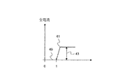
概説
図1は本発明のディスプレイシステム10のブロック図を示す。非線形入力信号11は、ELサブピクセル内のELエミッターからの特定の光強度を指示する。この信号11は、ビデオ復号器、画像処理経路、又は別の信号源から到来することができ、デジタル又はアナログとすることができ、非線形又は線形に符号化することができる。たとえば、非線形入力信号は、sRGBコード値(IEC 61966−2−1:1999+A1)又はNTSC輝度(luma)電圧とすることができる。どのような信号源及び信号形式であっても、その信号は、変換器12によって、デジタル形式に、かつ線形電圧のような線形領域に優先的に変換されることができ、それについては、「領域間処理及びビット深度」において下記でさらに検討される。変換の結果は線形コード値になり、そのコード値は指示される駆動電圧を表すことができる。
Overview FIG. 1 shows a block diagram of a
補償器13は線形コード値を受信し、その線形コード値は、ELサブピクセルから指示される特定の光強度に対応することができる。むらによって引き起こされる駆動トランジスタ及びELエミッター内の変動、並びにELサブピクセル内の駆動トランジスタ及びELエミッターの或る期間にわたる動作によって引き起こされる駆動トランジスタ及びELエミッター内の変動の結果として、ELサブピクセルは一般的に、線形コード値に応じて、指示された光強度を生成しなくなる。補償器13は、ELサブピクセルが指示された輝度を生成することになる変更済み線形コード値を出力し、それにより、駆動トランジスタ及びELエミッターの或る期間にわたる動作によって引き起こされる駆動トランジスタ及びELエミッターの特性の変動、並びに駆動トランジスタ及びELエミッターの特性のサブピクセル間の変動を補償する。補償器の動作は、「実施態様」において下記でさらに検討される。
The
補償器13からの変更済み線形コード値はソースドライバ14に渡され、ソースドライバはデジタル/アナログコンバータとすることができる。ソースドライバ14は、変更済み線形コード値に応答して、駆動トランジスタ制御信号を生成し、その信号は、アナログ電圧若しくはアナログ電流、又はパルス幅変調波形のようなデジタル信号とすることができる。好ましい実施形態では、ソースドライバ14は、線形入力−出力関係を有するソースドライバ、又はそのガンマ電圧が概ね線形な出力を生成するように設定される、従来のLCDソースドライバ若しくはOLEDソースドライバとすることができる。後者の場合、線形性から逸脱すると、結果の品質に影響が及ぼされることになる。また、ソースドライバ14は、たとえば、同じ譲受人に譲渡されるKawabeによる国際公開第2005/116971号において教示されるような、時分割(デジタル駆動)ソースドライバとすることもできる。デジタル駆動ソースドライバからのアナログ電圧は、補償器からの出力信号に応じた時間の長さだけ、光出力を指示する所定のレベルに設定される。対照的に、従来のソースドライバは、或る決まった長さの時間(一般的には、フレーム全体)だけ、補償器からの出力信号に依存するレベルのアナログ電圧を与える。ソースドドライバは、1つ又は複数の駆動トランジスタ制御信号を同時に出力することができる。パネルは、それぞれ一度に1つのサブピクセルのための駆動トランジスタ制御信号を出力する、複数のソースドライバを有することが好ましい。
The modified linear code value from the
ソースドライバ14によって生成される駆動トランジスタ制御信号は、ELサブピクセル15に与えられる。この回路は、「ディスプレイ構成要素の説明」において下記で検討される。アナログ電圧がELサブピクセル15内の駆動トランジスタのゲート電極に与えられると、駆動トランジスタ及びELエミッターを通って電流が流れ、ELエミッターが光を放射する。一般的に、ELエミッターを通って流れる電流とエミッターの光出力の輝度との間には線形の関係があり、駆動トランジスタに印加される電圧とELエミッターを通って流れる電流との間には非線形の関係がある。それゆえ、1フレーム中にELエミッターによって放射される光の全量は、ソースドライバ14からの電圧の非線形関数とすることができる。
The drive transistor control signal generated by the
ELサブピクセルを通って流れる電流は、「データ収集」において下記でさらに検討されるように、電流測定回路16によって特定の駆動条件下で測定される。ELサブピクセルのための測定された電流は、補償器に、指示された駆動信号を調整するために必要とする情報を提供する。これは、「アルゴリズム」において下記でさらに検討する。
The current flowing through the EL subpixel is measured by the
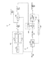
ディスプレイ構成要素の説明
図9は、OLEDエミッターのようなELエミッターに電流を流すELサブピクセル15、及び関連回路部を示す。ELサブピクセル15は、駆動トランジスタ201と、ELエミッター202と、オプションでストレージキャパシタ1002及び選択トランジスタ36とを備える。第1の電圧供給源211(「PVDD」)は正とすることができ、第2の電圧供給源206(「Vcom」)は負とすることができる。ELエミッター202は、第1の電極207及び第2の電極208を有する。駆動トランジスタは、ゲート電極203と、駆動トランジスタのドレインすることができる第1の供給電極204と、駆動トランジスタのソースとすることができる第2の供給電極205とを有する。オプションでは選択トランジスタ36を通して、駆動トランジスタ制御信号をゲート電極203に与えることができる。駆動トランジスタ制御信号は、ストレージキャパシタ1002に格納することができる。第1の供給電極204は、第1の電圧供給源211に電気的に接続される。第2の供給電極205は、ELエミッターに電流を流すために、ELエミッター202の第1の電極207に電気的に接続される。ELエミッターの第2の電極208は、第2の電圧供給源206に電気的に接続される。電圧供給源は通常ELパネル外に配置される。電気的接続は、スイッチ、バス線、導通トランジスタ、又は電流のための経路を提供することができる他のデバイス若しくは構造を通して行なうことができる。
Display Component Description FIG. 9 shows an
本発明の1つの実施形態では、第1の供給電極204は、PVDDバス線1011を通して第1の電圧供給源211に電気的に接続され、第2の電極208は、シートカソード1012を通して第2の電圧供給源206に電気的に接続され、選択トランジスタ36がゲート線34によってアクティブにされると、列線32aにわたって、ソースドライバ14によってゲート電極203に駆動トランジスタ制御信号が与えられる。
In one embodiment of the invention, the
図2は、システム10との関連でELサブピクセル15を示しており、そのシステムは、図1に示されるような、非線形入力信号11、コンバータ12、補償器13及びソースドライバ14を含む。上記のように、駆動トランジスタ201は、ゲート電極203と、第1の供給電極204と、第2の供給電極205とを有する。ELエミッター202は、第1の電極207及び第2の電極208を有する。そのシステムは、電圧供給源211及び206を有する。
FIG. 2 shows an
漏れを無視すると、同じ電流、すなわち、駆動電流が、第1の電圧供給源211から、第1の供給電極204及び第2の供給電極205を通り、ELエミッター電極207及び208を通って、第2の電圧供給源206まで流れる。駆動電流は、ELエミッターが光を放射するもとになる電流である。それゆえ、電流は、この駆動電流経路内の任意の点で測定することができる。第1の電圧供給源211において、ELパネル外で電流を測定し、ELサブピクセルを複雑にしないようにすることができる。駆動電流は本明細書においてIdsと呼ばれ、駆動トランジスタのドレイン端子及びソース端子を通って流れる電流である。
Neglecting the leakage, the same current, that is, the drive current, passes from the
データ収集
ハードウエア
さらに図2を参照すると、パネル上にあるどの特殊な電子回路にも頼ることなく、ELサブピクセル15の電流を測定するために、本発明は、電流ミラーユニット210、相関ダブルサンプリング(CDS)ユニット220、並びにオプションでアナログ/デジタルコンバータ(ADC)230及びステータス信号生成ユニット240を含む測定用回路16を用いる。
Data Acquisition Hardware Still referring to FIG. 2, to measure the current in the
ELサブピクセル15は、駆動トランジスタ201のゲート電極203上の測定基準ゲート電圧(図4A 510)に対応する電流において測定される。この電圧を生成するために、測定するときに、ソースドライバ14が試験電圧源としての役割を果たし、ゲート電極203に測定基準ゲート電圧を与える。選択されるしきい値電流よりも小さな測定電流に対応する測定基準ゲート電圧を選択することによって、都合の良いことに、測定をユーザの目に見えないようにしておくことができる。選択されるしきい値電流は、ELエミッターから目に見えるほどの光を放射するために必要とされる電流よりも小さくなるように、たとえば、1.0nit以下になるように選択することができる。測定が行なわれるまで、測定電流はわからないので、測定基準ゲート電圧は、モデル化によって、選択されるしきい値電流未満の選択されたヘッドルームパーセンテージである予想電流に対応するように選択することができる。
The
電流ミラーユニット210は、電圧供給源211に取り付けられているが、駆動電流経路内の任意の場所に取り付けることができる。第1の電流ミラー212が、スイッチ200を通して、ELサブピクセル15に駆動電流を供給し、その出力213においてミラー電流を生成する。ミラー電流は、駆動電流に等しいか、又は駆動電流の関数とすることができる。たとえば、ミラー電流を駆動電流の倍数とし、付加的な測定システム利得を与えることができる。第2の電流ミラー214及びバイアス供給源215は、第1の電流ミラー212にバイアス電流を印加し、パネルから見た第1の電流ミラーのインピーダンスを下げて、測定回路の反応速度を有利に上げる。この回路は、測定回路に電流が引き込まれることから生じる電流ミラーの電圧変化に起因して測定される、ELサブピクセルを通る電流の変化も低減する。これは、電流に応じて駆動トランジスタ端子における電圧を変更する可能性がある単純な検出抵抗器のような、他の電流測定オプションよりも信号対雑音比を有利に改善する。最後に、電流/電圧(I/V)コンバータ216が、第1の電流ミラーからのミラー電流を、さらに処理するために電圧信号に変換する。I/Vコンバータ216は、トランスインピーダンス増幅器又はローパスフィルタを含むことができる。
The
スイッチ200は、リレー又はFETとすることができ、測定用回路を、駆動トランジスタ201の第1の電極及び第2の電極を通って流れる駆動電流に選択的に電気的に接続することができる。測定中に、スイッチ200は、測定を可能にするために第1の電圧供給源211を第1の電流ミラー212に電気的に接続することができる。通常動作中に、スイッチ200は、第1の電圧供給源211を、第1の電流ミラー212ではなく、第1の供給電極204に直に電気的に接続することができ、それにより、測定用回路を駆動電流の流れから除去することができる。これにより、測定回路部は、パネルの通常動作に影響を及ぼさなくなる。また、これによって、電流ミラー212及び214内のトランジスタのような、測定回路の構成要素のサイズを、動作電流のためにではなく、測定電流のためだけに決めることができるようになるので有利である。通常動作は一般的に、測定よりもはるかに多くの電流を引き込むので、これにより、測定回路のサイズ及びコストを大幅に削減できるようになる。
The
サンプリング
電流ミラーユニット210によって、単一の時点におけるELサブピクセルのための電流を測定できるようになる。信号対雑音比を改善するために、一実施形態において、本発明は相関ダブルサンプリングを用いる。
The sampling
ここで図3を参照し、図2も参照すると、ELサブピクセル15がオフであるとき、測定49が行なわれる。したがって、そのELサブピクセルは暗電流を引き込んでいるが、それは0又はわずかな漏れ量とすることができる。暗電流が0でない場合には、ELサブピクセル15の電流の測定と混同しないようにできることが好ましい。時刻1において、ELサブピクセル15が起動され、測定回路16を用いて、その電流41が測定される。具体的には、測定されるのは、電流ミラーユニット210からの電圧信号であり、それは、上記で検討されたように、第1及び第2の電流供給源を通って流れる駆動電流Idsを表す。電流を表す電圧信号を測定することを、明確にするために、「電流を測定する」と言う。電流41は、第1のサブピクセルからの電流と、暗電流との和である。第1の測定値41と暗電流測定値49との間の差43が、第2のサブピクセルによって引き込まれる電流である。この方法によれば、サブピクセルの整定時間が許す限り迅速に、測定を行なうことができるようになる。
Referring now to FIG. 3, and also referring to FIG. 2,
再び図2を参照し、図3も参照すると、相関ダブルサンプリングユニット220が、測定された電流をサンプリングして、ステータス信号を生成する。ハードウエアでは、電流ミラーユニット210からの対応する電圧信号を図2のサンプルアンドホールドユニット221及び222内にラッチすることによって、電流が測定される。電圧信号は、I/Vコンバータ216によって生成される電圧信号とすることができる。差動増幅器223が、連続するサブピクセル測定値間の差をとる。サンプルアンドホールドユニット221の出力は、差動増幅器223の正端子に電気的に接続され、ユニット222の出力は、増幅器223の負端子に電気的に接続される。たとえば、電流49が測定されるとき、その測定値はサンプルアンドホールドユニット221内にラッチされる。その後、電流41が測定される(ユニット221内にラッチされる)前に、ユニット221の出力が第2のサンプルアンドホールドユニット222内にラッチされる。その後、電流41が測定される。これにより、ユニット222内に電流49が残り、ユニット221内に電流41が残る。したがって、差動増幅器の出力、すなわち、ユニット221内の値からユニット222内の値をマイナスしたものは、電流41(を表す電圧信号)から電流49(を表す電圧信号)をマイナスしたもの、すなわち、差43である。種々の駆動レベル(ゲート電圧又は電流密度)において連続して測定を行ない、そのサブピクセルのためのI−V曲線を形成することができる。
Referring again to FIG. 2 and also to FIG. 3, the correlated
差動増幅器223のアナログ又はデジタル出力は補償器13に直に与えることができる。代替的には、アナログ/デジタルコンバータ230が、好ましくは、差動増幅器223の出力をデジタル化して、補償器13にデジタル測定データを与えることができる。
The analog or digital output of the differential amplifier 223 can be provided directly to the
測定回路16は、好ましくは、ステータス信号生成ユニット240を含むことができ、ステータス信号生成ユニットは、差動増幅器223の出力を受信し、さらに処理を実行して、ELサブピクセルのためのステータス信号を与える。ステータス信号はデジタル又はアナログとすることができる。図5Bを参照すると、ステータス信号生成ユニット240が、明確にするために、補償器13との関連で示される。種々の実施形態において、ステータス信号生成ユニット240は、サブピクセルについてのデータを保持するためのメモリ619を含むことができる。
The
本発明の第1の実施形態では、電流差、たとえば、43を、対応するサブピクセルのためのステータス信号とすることができる。この実施形態では、ステータス信号生成ユニット240は、電流差に関する一次変換を実行することができるか、又はそれを変更せずに渡すことができる。測定基準ゲート電圧においてサブピクセルを通って流れる電流(43)は、サブピクセル内の駆動トランジスタ及びELエミッターの特性に依存し、それゆえ、意味があるように、それらの特性を表す。電流差43はメモリ619に格納することができる。
In the first embodiment of the present invention, the current difference, eg 43, can be the status signal for the corresponding sub-pixel. In this embodiment, the status
第2の実施形態では、メモリ619がELサブピクセル15のターゲット信号i0611を格納する。また、メモリ619は、ELサブピクセルの直近の電流測定値i1612も格納し、それは、サブピクセルのための測定回路によって直近に測定された値とすることができる。また、測定値612は、複数の測定値の平均、測定値の経時的な指数重み付け移動平均、又は当業者に明らかである他の平滑化方法の結果とすることもできる。ターゲット信号i0611及び現在の測定値i1612を、以下に説明されるように比較して、パーセント電流613を与えることができ、パーセント電流は、ELサブピクセルのためのステータス信号とすることができる。サブピクセルのためのターゲット信号は、そのサブピクセルの現在の測定値とすることができ、それゆえ、パーセント電流は、それぞれの駆動トランジスタ及びELエミッターの或る期間にわたる動作によって引き起こされる駆動トランジスタ及びELエミッターの特性の変動を表すことができる。
In the second embodiment, the
メモリ619は、RAM、フラッシュメモリのような不揮発性RAM、及びEEPROMのようなROMを含むことができる。一実施形態では、i0の値はEEPROMに格納され、i1の値はフラッシュに格納される。
The
雑音源
実際には、電流波形はきれいなステップではない可能性があるので、波形が整定するのを待った後にのみ測定を行なうことができる。各サブピクセルを何度も測定し、合わせてその平均をとることもできる。そのような測定は、連続して、又は別々の測定パスにおいて行なうことができる。電圧供給源206と211との間のキャパシタンスは、整定時間に加算することができる。このキャパシタンスは、通常の動作において一般的であるように、パネルに内在するか、外部キャパシタによって与えることができる。測定を行なう間に外部キャパシタを電気的に切断するために用いることができるスイッチを設けることが有利となる場合がある。
Noise sources In practice, the current waveform may not be a clean step, so measurements can only be taken after waiting for the waveform to settle. Each subpixel can be measured many times and averaged together. Such measurements can be performed continuously or in separate measurement paths. The capacitance between the
任意の電圧供給源での雑音が、電流測定値に影響を及ぼす。たとえば、ゲートドライバが行を非アクティブにするために用いる電圧供給源(多くの場合に、VGL又はVoffと呼ばれ、通常約−8VDCである)での雑音は選択トランジスタを介して駆動トランジスタに容量性結合し、その電流に影響を及ぼす可能性があり、それにより、電流測定値の雑音を多くする。パネルが複数の電源領域、たとえば、分割供給面を有する場合には、それらの領域はパラレルに測定することができる。そのような測定は、領域間で雑音を分離し、測定時間を短縮することができる。 Noise at any voltage source affects the current measurement. For example, noise at the voltage source used by the gate driver to deactivate a row (often referred to as VGL or Voff, which is typically about -8 VDC) is capacitive to the drive transistor through the select transistor. Can couple and affect the current, thereby making the current measurement noisy. If the panel has a plurality of power supply areas, for example split supply surfaces, these areas can be measured in parallel. Such measurements can separate noise between regions and reduce measurement time.
ソースドライバが切り替わるときはいつでも、雑音過渡現象が、電力供給面、及び個々のサブピクセルに結合して、測定雑音を引き起こす可能性がある。この雑音を低減するために、ソースドライバからの制御信号は、一定に保つことができる。これによってソースドライバ過渡雑音が除去される。 Whenever the source driver switches, noise transients can couple to the power supply plane and the individual subpixels, causing measurement noise. In order to reduce this noise, the control signal from the source driver can be kept constant. This eliminates source driver transient noise.
電流安定性
これまでの検討では、一旦、サブピクセルがオンになり、或る電流に整定すると、その列の残りの部分に対してその電流のままであると仮定する。その仮定を破る可能性がある2つの作用が、ストレージキャパシタ漏れ及びサブピクセル内作用である。
Current Stability Previous studies assume that once a subpixel is turned on and settles to a current, it remains at that current for the rest of the column. Two actions that can break that assumption are storage capacitor leakage and sub-pixel effects.
図9を参照すると、ELサブピクセル15内の選択トランジスタ36の漏れ電流が、ストレージキャパシタ1002上の電荷を徐々に放出する可能性があり、駆動トランジスタのゲート電圧201、ひいては、引き込まれる電流が変化する。さらに、列線32が経時的に値を変化させている場合には、それはAC成分を有し、それゆえ、選択トランジスタの寄生キャパシタンスを通してストレージキャパシタに結合する可能性があり、ストレージキャパシタの値、ひいては、サブピクセルによって引き込まれる電流が変化する。
Referring to FIG. 9, the leakage current of the
ストレージキャパシタの値が安定している場合であっても、サブピクセル内作用が測定を損なう可能性がある。一般的なサブピクセル内作用はサブピクセルの自己発熱であり、それは、サブピクセルによって引き込まれる電流を経時的に変化させる可能性がある。a−Si TFTのドリフト移動度は温度の関数である。温度が上昇すると、移動度が大きくなる(Kagan & Andry, op. cit., sec. 2.2.2, pp. 42−43)。電流が、駆動トランジスタを通って流れるとき、駆動トランジスタ内及びELデバイス内の電力損により、サブピクセルが加熱されるので、トランジスタの温度が上昇し、それゆえ、移動度が大きくなる。さらに、熱はVoledを下げる。OLEDが駆動トランジスタのソース端子に取り付けられる場合は、これにより、駆動トランジスタのVgsが上昇する可能性がある。これらの作用によって、トランジスタを通って流れる電流量が増加する。通常の動作では、パネルが表示している画像の平均的な表示内容に基づいて、パネルが平均温度に安定することができるので、自己発熱は些細な作用である可能性がある。しかしながら、サブピクセル電流を測定するとき、自己発熱は測定を損なう可能性がある。 Even when the value of the storage capacitor is stable, sub-pixel effects can impair the measurement. A common sub-pixel effect is sub-pixel self-heating, which can change the current drawn by the sub-pixel over time. The drift mobility of a-Si TFT is a function of temperature. As the temperature increases, the mobility increases (Kagan & Andry, op. Cit., Sec. 2.2.2, pp. 42-43). As current flows through the drive transistor, power loss in the drive transistor and in the EL device heats the subpixel, thus increasing the temperature of the transistor and thus increasing mobility. In addition, heat reduces V oled . If the OLED is attached to the source terminal of the drive transistor, this can increase the V gs of the drive transistor. These effects increase the amount of current flowing through the transistor. In normal operation, self-heating can be a trivial effect because the panel can stabilize to an average temperature based on the average display content of the image displayed by the panel. However, when measuring the subpixel current, self-heating can impair the measurement.
自己発熱作用及び同様の雑音シグネチャを生成する任意の他のサブピクセル内作用を補正するために、自己発熱を特徴付けて、各サブピクセルの既知の自己発熱成分から減算することができる。 In order to correct for any self-heating effects and any other in-subpixel effects that produce a similar noise signature, the self-heating can be characterized and subtracted from the known self-heating component of each subpixel.
自己発熱、及び電力損に起因する誤差は、低い測定基準ゲート電圧を選択することにより低減することができるが(図4A 510)、電圧を高くするほど、信号対雑音比が改善される。これらの要因のバランスを保つために、パネル設計毎に測定基準ゲート電圧を選択することができる。 Although errors due to self-heating and power loss can be reduced by selecting a lower metric gate voltage (FIG. 4A 510), the higher the voltage, the better the signal to noise ratio. To maintain a balance of these factors, a measurement reference gate voltage can be selected for each panel design.
アルゴリズム
図4Aを参照すると、I−V曲線501は、経時変化前のサブピクセルの測定された特性である。I−V曲線502は、経時変化後のサブピクセルの測定された特性である。曲線501、及び502は、異なる電流レベルにおける同一の電圧差503、504、505、及び506によって示されるように、主に水平方向のシフトによって分離される。すなわち、経時変化の主な作用は、ゲート電圧軸上で一定の量だけI−V曲線をシフトすることである。これは、MOSFET飽和領域の駆動トランジスタの式、Id=K(Vgs−Vth)2に従う(Lurch, N. Fundamentals of electronics, 2e. New York: John Wiley & Sons, 1971, pg. 110):駆動トランジスタが動作すると、Vthは増加し、そして、Vthが増加すると、それに応じてVgsが増加して、Idを一定に保持する。それゆえ、Vgsを一定にする結果として、Vthが増加すると、Idsが小さくなる。
Algorithm Referring to FIG. 4A, an
測定基準ゲート電圧510において、経時変化していないサブピクセルは、点511で表される電流を生成した。しかしながら、経時変化したサブピクセルは、そのゲート電圧において、点512aで表される、より低い電流量を生成した。点511及び521aは、異なる時間において取り込まれる同じサブピクセルの2つの測定値とすることができる。例えば、点511は、製造時の測定値とすることができ、点512aは、顧客がいくらか使用した後の測定値とすることができる。点512aにおいて表される電流は、電圧513(点512b)で駆動されるときに、経時変化していないサブピクセルであれば生成していたので、電圧シフトΔVth514は、電圧510と513との間の電圧差として計算される。したがって、電圧シフト514は、経時変化した曲線を経時変化していな曲線に戻すために必要とされるシフトである。この例では、ΔVth514は、2V弱である。その際、Vthシフトを補償し、経時変化したサブピクセルを経時変化していないサブピクセルが有したのと同じ電流に駆動するために、電圧シフト514が、指示された全ての駆動電圧(線形コード電圧)に加算される。さらに処理するために、電流512aを電流511で割った値として、パーセント電流が計算される。したがって、経時変化していないサブピクセルは、100%電流を有することになる。パーセント電流は、本発明によるいくつかのアルゴリズムにおいて用いられる。極端な環境雑音によって引き起こされる場合があるような、任意の負の電流読み値511は、0にクリップされるか、又は無視することができる。パーセント電流は常に測定基準ゲート電圧510において計算されることに留意されたい。
At the measurement
一般的に、経時変化したサブピクセルの電流は、経時変化していないサブピクセルの電流よりも高いか、又は低い可能性がある。例えば、温度が高くなるほど、多くの電流が流れるので、高温環境におけるわずかに経時変化したサブピクセルは、低温環境における経時変化していないサブピクセルよりも多くの電流を引き込む可能性がある。本発明の補償アルゴリズムは、いずれの場合も取り扱うことができる:ΔVth514は、正である可能性も、負である可能性もある(又は、経時変化していないピクセルの場合は0)。同様に、パーセント電流は、100%より大きい可能性も、小さい可能性もある(又は、経時変化していないピクセルの場合に、厳密に100%)。 In general, the current of a subpixel that has changed over time may be higher or lower than the current of a subpixel that has not changed over time. For example, the higher the temperature, the more current flows, so a sub-pixel that has changed slightly over time in a high temperature environment may draw more current than a sub-pixel that does not change over time in a low temperature environment. The compensation algorithm of the present invention can handle either case: ΔV th 514 can be positive or negative (or 0 for non-aging pixels). Similarly, the percent current may be greater or less than 100% (or exactly 100% for pixels that have not changed over time).
Vthシフトに起因する電圧差は、全ての電流で同じであるので、I−V曲線上のいずれか1つの点を測定して、この差を求めることができる。一実施形態では、高いゲート電圧において測定が行われ、測定の信号対雑音比を高めることが有利であるが、曲線上の任意のゲート電圧を用いることができる。 Since the voltage difference due to the V th shift is the same for all currents, this difference can be obtained by measuring any one point on the IV curve. In one embodiment, measurements are made at a high gate voltage and it is advantageous to increase the signal-to-noise ratio of the measurement, but any gate voltage on the curve can be used.
Voledシフトは、二次的な経時変化作用である。ELデバイスが動作するのに応じて、Voledがシフトし、それにより、経時変化したI−V曲線がもはや経時変化していない曲線の単なるシフトではなくなる。これは、Voledが電流と共に非線形に上昇するためであり、Voledシフトが及ぼす影響は、高電流では低電流とは異なるであろう。この作用によって、I−V曲線は水平方向に伸長し、かつシフトする。Voledシフトを補償するために、異なる駆動レベルにおいて2回の測定を行い、曲線がどのくらい伸長したかを求めることができるか、又は負荷をかけてOLEDの通常のVoledシフトを特徴付けて、開ループでVoledの寄与を推定できるようにする。いずれも、許容可能な結果を生成することができる。 The Voled shift is a secondary aging effect. As the EL device operates, the V oled shifts so that the time-varying IV curve is no longer just a shift of the curve that is no longer time-varying. This is because V oled increases non-linearly with current, and the effect of the V oled shift will be different at high current than at low current. By this action, the IV curve extends and shifts in the horizontal direction. To compensate for the V oled shift, two measurements at different drive levels can be taken to determine how much the curve has stretched, or a load can be applied to characterize the normal V oled shift of the OLED, Enable to estimate the contribution of Voled in an open loop. Either can produce acceptable results.
図4Bを参照すると、経時変化していないサブピクセルのI−V曲線501及び経時変化したサブピクセルのI−V曲線502が片対数目盛において示される。成分550は、Vthシフトに起因し、成分552は、Voledシフトに起因する。Voledシフトは、測定手段を備えたOLEDサブピクセルを、長時間にわたって通常の入力信号によって駆動し、Vth及びVoledを周期的に測定することによって特徴付けることができる。2つの測定は、測定手段を備えたサブピクセル上に、OLEDとトランジスタとの間にプローブ点を設けることによって、別々に行うことができる。この特徴付けを用いて、パーセント電流を、Vthシフトに対してだけではなく、適切なΔVth及びVoledに対してマッピングすることができる。
Referring to FIG. 4B, the non-time-varying
一実施形態では、ELエミッター202(図9)は、駆動トランジスタ201のソース端子に接続される。したがって、Voledの任意の変化が、駆動トランジスタのソース端子における電圧Vs、それゆえ、駆動トランジスタのVgsを変更するので、Idsに直に影響を及ぼす。
In one embodiment, EL emitter 202 (FIG. 9) is connected to the source terminal of
好ましい実施形態では、ELエミッター202は、たとえば、PMOS非反転構成において、駆動トランジスタ201のドレイン端子に接続され、その構成では、OLEDアノードは駆動トランジスタドレインに結合される。したがって、OLEDが駆動トランジスタのドレイン−ソース間経路と直列に接続されるので、Voledが上昇すると、駆動トランジスタ201のVdsが変化する。しかしながら、最新のOLEDエミッターは、所与の量の経時変化の場合に、旧式のエミッターよりもはるかに小さなΔVoledを有し、Vds変化の大きさ、それゆえ、Ids変化の大きさを低減する。
In a preferred embodiment, the
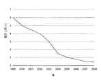
図10は、その寿命にわたる白色OLEDの場合の通常の電圧上昇ΔVoledのプロットを示す(T50、すなわち、20mA/cm2において測定される50%輝度まで)。このプロットは、OLED技術が改善されるのに応じて、ΔVoledが減少することを示す。このΔVoledの減少により、Vds変化が減少する。図4Aを参照すると、経時変化したサブピクセルの電流512aは、ΔVoledが小さな最新のOLEDエミッターの場合の方が、ΔVoledが大きな旧式のエミッターの場合よりも、電流511にはるかに近い。それゆえ、最新のOLEDエミッターの場合、旧式のエミッターの場合よりも、はるかに高感度の電流測定が要求される可能性がある。しかしながら、より高感度の測定ハードウエアは費用がかかる可能性がある。 FIG. 10 shows a plot of normal voltage rise ΔV oled for a white OLED over its lifetime (T50, ie up to 50% brightness measured at 20 mA / cm 2 ). This plot shows that ΔV oled decreases as OLED technology improves. This decrease in ΔV oled reduces the V ds change. Referring to Figure 4A, the current 512a of the aged subpixel, who if [Delta] V oled is small latest OLED emitters, than [Delta] V oled is a large old emitters, much closer to the current 511. Therefore, current OLED emitters may require much more sensitive current measurements than do older emitters. However, more sensitive measurement hardware can be expensive.
特別な測定感度のための要件は、電流を測定する間に、駆動トランジスタを線形の動作領域において動作させることによって緩和することができる。電子回路技術分野において既知であるように、薄膜トランジスタは、2つの異なる動作モード:線形(Vds<Vgs−Vth)及び飽和(Vds≧Vgs−Vth)において、感知できるほどの電流を流す(Lurch, op. cit., p. 111)。ELの応用例では、駆動トランジスタは通常飽和領域において動作し、Vds変動が電流に及ぼす影響を低減する。しかしながら、線形動作領域では、
Ids=K[2(Vgs−Vth)Vds−Vds 2]
であり(Lurch, op. cit., pg. 112)、電流IdsはVdsに大きく依存する。図9に示されるように、
Vds=(PVDD−Vcom)−Voled
であるので、線形領域におけるIdsはVoledに大きく依存する。それゆえ、駆動トランジスタ201の線形動作領域において電流を測定することは、飽和領域において同じ測定を行なうのに比べて、新品のOLEDエミッター(511)と経時変化したOLEDエミッター(512a)との間の測定電流の変化の大きさを大きくするので好都合である。
The requirement for special measurement sensitivity can be relaxed by operating the drive transistor in a linear operating region while measuring the current. As is known in the electronic circuit art, thin film transistors are sensitive to currents in two different modes of operation: linear (V ds <V gs −V th ) and saturation (V ds ≧ V gs −V th ). (Lurch, op. Cit., P. 111). In EL applications, the drive transistor normally operates in the saturation region, reducing the effect of V ds variations on the current. However, in the linear operating region,
I ds = K [2 (V gs −V th ) V ds −V ds 2 ]
(Lurch, op. Cit., Pg. 112), and the current I ds greatly depends on V ds . As shown in FIG.
V ds = (PVDD−V com ) −V oled
Therefore, I ds in the linear region greatly depends on Voled . Therefore, measuring the current in the linear operating region of the
それゆえ、本発明の一実施形態は、電圧コントローラーを含む。上記のように電流を測定する間に、電圧コントローラーは、第1の電圧供給源211及び第2の電圧供給源206のための電圧を制御し、試験電圧源として動作するソースドライバ14からの駆動トランジスタ制御信号を制御して、駆動トランジスタ201を線形領域において動作させることができる。たとえば、PMOS非反転構成では、電圧コントローラーは、PVDD電圧及び駆動トランジスタ制御信号を一定の値に保持し、Vcom電圧を上昇させて、Vgsを低減することなく、Vdsを低減することができる。VdsがVgs−Vth未満に降下するとき、駆動トランジスタは線形領域において動作していることになり、測定を行なうことができる。電圧コントローラーは、補償器内に収容することができる。また、電圧コントローラー及びシーケンスコントローラーが協調して測定中にトランジスタを線形領域において動作させる限り、電圧コントローラーは、シーケンスコントローラーとは別に設けることもできる。
Therefore, one embodiment of the present invention includes a voltage controller. During the current measurement as described above, the voltage controller controls the voltages for the
OLED効率損失は三次的な経時変化作用である。OLEDが経時変化すると、その効率が低下し、同じ電流量がもはや同じ量の光を生成しなくなる。光学センサー又は付加的な電子回路を必要とすることなく、これを補償するために、OLED効率損失をVthシフトの関数として特徴付けることができ、光出力をその以前のレベルに戻すために必要とされる余分な電流の量を推定できるようにする。測定手段を備えたOLEDサブピクセルを、長時間にわたって通常の入力信号によって駆動し、種々の駆動レベルにおいてVth、Voled及びIdsを周期的に測定することによって、OLED効率損失を特徴付けることができる。効率はIds/Voledとして計算することができ、その計算結果を、Vth又はパーセント電流と関連付けることができる。Vthシフトは簡単に逆にすることができるがOLED効率損失は簡単に逆にすることができないので、その特徴付けは、Vthシフトが常に順方向であるときに、より実効的な結果を達成することに留意されたい。Vthシフトが逆にされる場合には、OLED効率損失をVthシフトと関連付けるのは複雑になる可能性がある。さらに処理するために、上記のパーセント電流の計算と同じようにして、経時変化した効率を新品の効率で割った値として、パーセント効率を計算することができる。 OLED efficiency loss is a tertiary aging effect. As an OLED changes over time, its efficiency decreases and the same amount of current no longer produces the same amount of light. To compensate for this without the need for an optical sensor or additional electronics, the OLED efficiency loss can be characterized as a function of the Vth shift and required to return the light output to its previous level. To be able to estimate the amount of extra current that will be done. OLED sub-pixels equipped with measuring means can be driven by a normal input signal for a long time and the OLED efficiency loss can be characterized by periodically measuring V th , V oled and I ds at various drive levels. it can. Efficiency can be calculated as I ds / V oled and the result can be related to V th or percent current. Since the V th shift can be easily reversed, but the OLED efficiency loss cannot be reversed easily, the characterization is more effective when the V th shift is always forward. Note that this is achieved. If the V th shift is reversed, it can be complicated to associate the OLED efficiency loss with the V th shift. For further processing, the percent efficiency can be calculated in the same manner as the percent current calculation described above, with the time-dependent efficiency divided by the new efficiency.
図8を参照すると、種々の駆動レベルにおけるパーセント電流の関数としてパーセント効率の実験プロットが示されており、実験データの直線の当てはめ、たとえば、90も合わせて示される。そのプロットが示すように、任意の所与の駆動レベルにおいて、効率はパーセント電流に線形に関連付けられる。この線形モデルによって、実効的な開ループ効率補償が可能である。 Referring to FIG. 8, an experimental plot of percent efficiency as a function of percent current at various drive levels is shown, and a linear fit of experimental data, eg, 90, is also shown. As the plot shows, efficiency is linearly related to percent current at any given drive level. This linear model enables effective open loop efficiency compensation.
駆動トランジスタ及びELエミッターの動作に起因する経時的なVth及びVoledシフト並びにOLED効率損失を補償するために、ステータス信号生成ユニット240の上記の第2の実施形態を用いることができる。測定基準ゲート電圧510においてサブピクセル電流を測定することができる。点511における経時変化していない電流がターゲット信号i0611である。直近の経時変化したサブピクセルの電流測定値512aが、直近の電流測定値i1612である。パーセント電流613がステータス信号である。パーセント電流613は0(故障したピクセル)、1(変化無し)、1未満(電流損)、又は1より大きい値(電流利得)とすることができる。一般的に、直近の電流測定値は、好ましくはパネル製造時に得られた電流測定値とすることができるターゲット信号よりも低いので、0と1との間にある。
The above second embodiment of status
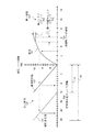
実施態様
図5Aを参照すると、補償器13の一実施形態が示される。補償器13への入力は線形コード値602であり、それは、ELサブピクセル15のための指示される駆動電圧を表すことができる。補償器13は、その線形コード値を変更して、ソースドライバのための変更済み線形コード値を生成し、それは、たとえば、補償済み電圧出力603とすることができる。補償器13は、4つの主なブロック:サブピクセルの製造後経過時間を求める(61)、オプションでOLED効率を補償する(62)、製造後経過時間に基づいて補償を決定する(63)及び補償する(64)を含むことができる。ブロック61及び62は主にOLED効率補償に関連し、ブロック63及び64は主に電圧補償、具体的には、Vth/Voled補償に関連する。
Implementation Referring to FIG. 5A, one embodiment of
図5Bはブロック61及び62の拡大図である。上記のように、格納されるターゲット信号i0611及び格納される直近の測定値i1612が読み出され、パーセント電流613、すなわち、サブピクセルのためのステータス信号が計算される。
FIG. 5B is an enlarged view of the
パーセント電流613は次の処理ステージ63に送出され、パーセントOLED効率614を求めるためにモデル695にも入力される。モデル695は効率614を出力し、その効率は、直近の測定時に所与の電流の場合に放射された光の量を、製造時にその電流の場合に放射された光の量で割った値である。電流利得があるピクセルの場合、効率損失を計算するのは難しい可能性があるので、1より大きな任意のパーセント電流は1、すなわち無損失の効率を生成することができる。OLED効率が指示される電流に依存する場合、破線の矢印によって示されるように、モデル695は線形コード値602の関数とすることもできる。モデル695への入力として線形コード値602を含むか否かは、パネル設計の寿命試験及びモデル化によって決定することができる。
The percent current 613 is delivered to the
図11を参照すると、本発明者らは、効率が一般的に電流密度及び製造後経過時間の関数であることに気がついている。図11の各曲線は、電流密度Idsをエミッター面積で割った値と、特定の時点まで経時変化したOLEDの場合の効率(Loled/Ids)との関係を示す。製造後経過時間は、当該技術分野において既知であるT表記を用いて凡例において示される。たとえば、T86は、たとえば、20mA/cm2の試験電流密度における86%効率を意味する。 Referring to FIG. 11, the inventors have noticed that efficiency is generally a function of current density and post production time. Each curve in FIG. 11 shows the relationship between the value obtained by dividing the current density I ds by the emitter area and the efficiency (L oled / I ds ) in the case of an OLED that has changed over time until a specific time point. Elapsed time after manufacture is indicated in the legend using the T notation known in the art. For example, T86 means, for example, 86% efficiency at a test current density of 20 mA / cm 2 .
図6Bを再び参照すると、それゆえ、モデル695は、電流密度及び製造後経過時間を補償するための指数項(又は何らかの他の実施態様)を含む。電流密度は、指示される電圧を表す線形コード値602に線形に関連付けられる。それゆえ、モデル695がその一部である補償器13は、ステータス信号(613)及び線形コード値(602)の両方に応答して線形コード値を変更し、ELサブピクセル内の駆動トランジスタ及びELエミッターの特性の変動、そして具体的には、ELサブピクセル内のELエミッターの効率の変動を補償することができる。
Referring again to FIG. 6B, therefore, the
同時に、補償器は、線形コード値602、たとえば、指示される電圧を受信する。この線形コード値602は、所望の電流621を求めるために製造時に測定されたパネルの元のI−V曲線691に通される。所望の電流の場合の光出力をその製造時の値に戻すために、演算628において、これがパーセント効率614で除算される。結果として生成されるブースト電流は、その後、曲線691の反転である曲線692に通され、効率損失がある場合に、どの指示電圧が望まれる光の量を生成するかを判断する。曲線692からの値は、効率調整済み電圧622として次のステージに渡される。
At the same time, the compensator receives a
効率補償が望まれない場合には、線形コード値602は、オプションのバイパス経路626として示されるように、変更されずに効率調整済み電圧622として次のステージに送られる。効率補償が望まれているか否かに関わらずパーセント電流613は計算されるが、パーセント効率614は計算不要である。
If efficiency compensation is not desired, the
図5Cは、図5Aのブロック63及び64の拡大図である。それは、先行するステージから、パーセント電流613及び効率調整済み電圧622を受信する。ブロック63「補償を得る」は、反転I−V曲線692を通してパーセント電流613をマッピングし、その結果を測定基準ゲート電圧(510)から減算し(図4A 513)、VthシフトΔVth631を見つける。ブロック64「補償する」は演算633を含み、その演算は、式1に与えられるように、補償済み電圧出力603を計算する。
Vout=Vin+ΔVth(1+α(Vg,ref−Vin)) (式1)
ただし、Voutは、補償済み電圧出力603であり、ΔVthは電圧シフト631であり、αはアルファ値632であり、Vg,refは測定基準ゲート電圧510であり、Vinは効率的な調整済み電圧622である。補償済み電圧出力は、ソースドライバのための変更済み線形コード値として表すことができ、駆動トランジスタ及びELエミッターの或る期間にわたる動作によって引き起こされる駆動トランジスタ及びELエミッターの特性の変動を補償する。
FIG. 5C is an enlarged view of
V out = V in + ΔV th (1 + α (V g, ref −V in )) (Formula 1)
Where V out is the compensated
直線的なVthシフトの場合、αは0であり、演算633は、効率調整済み電圧622にVthシフト量を加算することに簡約される。任意の特定のピクセルの場合に、新たな測定が行なわれるまで、加算する量は一定である。この場合、演算633において加算する電圧は、測定が行なわれた後に予め計算することができ、ブロック63及び64を、格納された値を探索し、それを加算することに短縮できるようになる。これは、ロジックを大幅に節約することができる。
In the case of a linear V th shift, α is 0, and the
領域間処理及びビット深度
当該技術分野において既知の画像処理経路は通常非線形コード値(NLCV)、すなわち、輝度に対して非線形の関係を有するデジタル値を生成する(Giorgianni & Madden著「Digital Color Management: encoding solutions」(Reading, Mass.: Addison-Wesley, 1998. Ch. 13, pp. 283-295))。非線形出力を用いることは、通常のソースドライバの入力領域に一致し、かつコード値精度範囲を人の目の精度範囲に一致させる。しかしながら、Vthシフトは電圧領域動作であるので、線形電圧空間において実施されることが好ましい。ソースドライバを使用し、ソースドライバの前に領域変換を実行して、非線形領域画像処理経路を線形領域補償器と実効的に統合することができる。この検討はデジタル処理に関するものであるが、アナログ又はデジタル/アナログ混在システムにおいても同様の処理を実行できることに留意されたい。また、補償器は、電圧以外の線形空間において動作できることにも留意されたい。たとえば、補償器は線形電流空間において動作することができる。
Inter-region processing and bit depth Image processing paths known in the art typically generate non-linear code values (NLCV), ie digital values that have a non-linear relationship to luminance ("Digital Color Management: by Giorgianni & Madden: encoding solutions "(Reading, Mass .: Addison-Wesley, 1998. Ch. 13, pp. 283-295)). Using a non-linear output matches the input range of a normal source driver and matches the code value accuracy range to the human eye accuracy range. However, since the V th shift is a voltage domain operation, it is preferably implemented in a linear voltage space. A source driver can be used to perform the domain transformation before the source driver to effectively integrate the nonlinear domain image processing path with the linear domain compensator. It should be noted that although this discussion concerns digital processing, similar processing can be performed in analog or mixed digital / analog systems. It should also be noted that the compensator can operate in a linear space other than voltage. For example, the compensator can operate in a linear current space.
図6を参照すると、象限I 127において領域変換ユニット12、そして象限II 137において補償器13の効果に関するジョーンズダイアグラム表示が示される。この図は、これらのユニットの数学的な効果を示しており、それらのユニットが如何に実現されるかを示すものではない。これらのユニットの実施態様はアナログ又はデジタルとすることができ、ルックアップテーブル又は関数を含むことができる。象限Iは領域変換ユニット12の動作を表す。軸701上の、非線形コード値(NLCV)とすることができる非線形入力信号が、変換711を通してマッピングすることによって変換され、軸702上に線形コード値(LCV)を形成する。象限IIは補償器13の動作を表す。軸702上のLCVが721及び722のような変換を通してマッピングされ、軸703上に変更済み線形コード値(CLCV)を形成する。
Referring to FIG. 6, a Jones diagram representation is shown for the effect of the
象限Iを参照すると、領域変換ユニット12がサブピクセル毎にそれぞれのNLCVを受信し、それをLCVに変換する。この変換は、輪郭化及び粒状の黒い染み(crushed blacks)のような目に見える不快なアーティファクトを避けるのに十分な分解能を用いて実行されるべきである。デジタルシステムでは、NLCV軸701は、図6に示されるように、量子化することができる。量子化されたNLCVの場合、LCV軸702は、2つの隣接するNLCV間の変換711の最も小さな変化を表すのに十分な分解能を有するはずである。これは、NLCVステップ712及び対応するLCVステップ713として示される。LCVは、その名の通りに線形であるので、LCV軸702全体の分解能は、ステップ713を表すのに十分にすべきである。それゆえ、画像情報の損失を避けるために、LCVは、NLCVよりも細かい分解能を用いて規定できることが好ましい。その分解能は、ナイキストサンプリング定理から類推して、ステップ713の2倍とすることができる。
Referring to quadrant I,
変換711は、経時変化していないサブピクセルのための理想的な変換である。それは、任意のサブピクセル又はパネル全体の経時変化との関係を持たない。具体的には、変換711は、いかなるVth、Voled又はOLEDの効率変化によっても変更されない。全ての色に対して1つの変換が存在することができるか、又は色毎に1つの変換が存在することができる。領域変換ユニットは、変換711を通して、画像処理経路を補償器から切り離し、2つが情報を共有する必要なく一緒に動作できるようにするので好都合である。これは、両方の実施態様を簡単にする。領域変換ユニット12は、LCDソースドライバに類似のルックアップテーブル又は関数として実施することができる。
象限IIを参照すると、補償器13が、LCVを変更済み線形コード値(CLCV)に変更する。図6は簡単な事例であり、一般性を失うことなく、直線的なVthシフトを補正する。直線的なVthシフトは、LCVからCLCVへの直線的な電圧シフトによって補正することができる。他の経時変化作用は、「実施態様」において上記で説明されたように取り扱うことができる。 Referring to quadrant II, compensator 13 changes the LCV to a modified linear code value (CLCV). FIG. 6 is a simple example, which corrects a linear Vth shift without losing generality. The linear V th shift can be corrected by a linear voltage shift from LCV to CLCV. Other aging effects can be handled as described above in the “Embodiments”.
変換721は、経時変化したサブピクセルの場合の補償器の挙動を表す。この場合、CLCVはLCVと同じとすることができる。変換722は、経時変化したサブピクセルの場合の補償器の挙動を表す。この場合、CLCVは、LCVに該当のサブピクセルのVthシフトを表すオフセットをプラスしたものとすることができる。結果として、補償のためのヘッドルームを与えるために、CLCVは一般的に、LCVよりも大きな範囲を必要とすることになる。たとえば、サブピクセルが、新品であるときには256LCVを必要とし、その寿命にわたる最大シフトが128LCVである場合には、大きく経時変化したサブピクセルの補償をクリップするのを避けるために、CLCVは、最大で384=256+128までの値を表すことができる必要がある。
図6は、領域変換ユニット及び補償器の作用の1つの完全な例を示す。図6の一点鎖線の矢印に従うと、3のNLCVが、象限Iにおいて示されるように、領域変換ユニット12によって、変換711を通して9のLCVに変換される。経時変化していないサブピクセルの場合、補償器13は、象限IIにおいて示されるように、変換721を通してそれを9のCLCVとして渡すことになる。12CLCVに類似のVthシフトを有する経時変化したサブピクセルの場合、9のLCVは、変換722を通して、9+12=21のCLCVに変換されることになる。
FIG. 6 shows one complete example of the operation of the domain conversion unit and the compensator. According to the dashed-dotted arrow in FIG. 6, 3 NLCVs are converted to 9 LCVs through the
一実施形態では、画像処理経路からのNLCVは9ビット幅である。LCVは11ビット幅である。非線形入力信号から線形コード値への変換は、LUT又は関数によって実行することができる。補償器は、所望の電圧を表す11ビット線形コード値を取り込み、12ビット変更済み線形コード値を生成し、ソースドライバ14に送る。その後、ソースドライバ14は、変更済み線形コード値に応答して、ELサブピクセルの駆動トランジスタのゲート電極を駆動することができる。補償器は、補償のためのヘッドルームを与えるために、すなわち、電圧範囲78を電圧範囲79に拡張し、同時に、最小線形コード値ステップ713の場合に必要とされるように、新たな拡張された範囲にわたって同じ分解能を保持するために、その入力よりも、その出力において大きなビット深度を有することができる。補償器出力範囲は、変換721の範囲より下に、かつその上に拡張することができる。
In one embodiment, the NLCV from the image processing path is 9 bits wide. The LCV is 11 bits wide. The conversion from a non-linear input signal to a linear code value can be performed by a LUT or function. The compensator takes an 11-bit linear code value representing the desired voltage, generates a 12-bit modified linear code value, and sends it to the
パネルの設計寿命にわたって最大のVthシフト、Voled上昇及び効率損失がどの程度であるかを判断するために各パネル設計を特徴付けることができ、補償器及びソースドライバは、補償するだけの十分な範囲を有することができる。この特徴付けは、標準的なトランジスタ飽和領域Idsの式を介して、要求される電流から要求されるゲートバイアス及びトランジスタ寸法に進むことができ、その後、経時的なa−Si劣化のための当該技術分野において知られている種々のモデルを介して、経時的なVthシフトに進むことができる。 Each panel design can be characterized to determine the maximum V th shift, Voled rise and efficiency loss over the panel design lifetime, and the compensator and source driver are sufficient to compensate Can have a range. This characterization can proceed from the required current to the required gate bias and transistor dimensions via the standard transistor saturation region I ds equation, and then for a-Si degradation over time. Through various models known in the art, one can proceed to V th shift over time.
動作の流れ
パネル設計特徴付け
このセクションは、特定のOLEDパネル設計の大量生産との関連で説明される。大量生産を開始する前に、その設計を特徴付けることができる。加速寿命試験を実行することができ、種々のレベルまで経時変化した種々のサンプル基板上の種々の色の種々のサブピクセルに対してI−V曲線を測定することができる。必要とされる測定の数及びタイプ、並びに経時変化レベルの数及びタイプは、特定のパネルの特性による。これらの測定値を用いて、値アルファ(α)を計算することができ、測定基準ゲート電圧を選択することができる。アルファ(図5C 項632)は、経時的な直線シフトからの偏差を表す値である。0のα値は、たとえば、Vthシフトのみの場合に当てはまるように、全ての経時変化が電圧軸上で直線的なシフトであることを示す。測定基準ゲート電圧(図4A 510)は、補償のために経時変化信号測定が行なわれる電圧であり、許容可能なS/N比を与えつつ、かつ電力損を低く抑えるように選択することができる。
Operational Flow Panel Design Characterization This section is described in the context of mass production of specific OLED panel designs. Before starting mass production, the design can be characterized. Accelerated life testing can be performed and IV curves can be measured for different subpixels of different colors on different sample substrates that have changed over time to different levels. The number and type of measurements required and the number and type of time-varying levels depends on the characteristics of the particular panel. Using these measurements, the value alpha (α) can be calculated and the measurement reference gate voltage can be selected. Alpha (FIG. 5C, term 632) is a value representing the deviation from the linear shift over time. An α value of 0 indicates that all temporal changes are linear shifts on the voltage axis, for example, as is the case with only the V th shift. The measurement reference gate voltage (FIG. 4A 510) is a voltage at which a time-varying signal measurement is performed for compensation, and can be selected to provide an acceptable S / N ratio and to keep power loss low. .
α値は最適化によって計算することができる。一例が表1に与えられる。複数の経時変化条件下で、複数のゲート電圧においてΔVthを測定することができる。その後、各ΔVthと測定基準ゲート電圧510におけるΔVthとの間で、ΔVth差が計算される。各ゲート電圧と測定基準ゲート電圧510との間でVg差が計算される。その後、式内のΔVthとして測定基準ゲート電圧510における適切なΔVthを用いて、かつ(Vg,ref−Vin)として適切な計算されたゲート電圧差を用いて、測定毎に式1の内項、ΔVth・α・(Vg,ref−Vin)を計算して、予測されるΔVth差を生成することができる。その後、α値を繰返し選択して、予測されるΔVth差と計算されたΔVth差との間の誤差を低減し、好ましくは数学的に最小限にすることができる。誤差は、最大差又はRMS差として表すことができる。Vg差の関数としてのΔVth差の最小二乗当てはめのような、当該技術分野において既知である代替の方法を用いることもできる。
The α value can be calculated by optimization. An example is given in Table 1. ΔV th can be measured at multiple gate voltages under multiple aging conditions. Then, between the [Delta] V th at the measurement

α及び測定基準ゲート電圧に加えて、特徴付けによって、上記のように、Vthシフトの関数としてのVoledシフト、Vthシフトの関数としての効率損失、サブピクセル当たりの自己発熱成分、最大Vthシフト、Voledシフト及び効率損失、並びに非線形/線形変換及び補償器において必要とされる分解能も決定することができる。必要とされる分解能は、同じ譲受人に譲渡される同時係属の米国特許出願公開第2008/0252653号のようなパネル較正手順に関連して特徴付けることができ、その開示は本明細書に援用される。下記で「現場において」で説明されるように、特徴付けによって、現場において特徴付け測定を行なうための条件、及び特定のパネル設計の場合に、ステータス信号生成ユニット240のどの実施形態を使用すべきであるかも決定することができる。これら全ての決定は、当業者が行うことができる。
In addition to the α and measurement reference gate voltage, the characterization, as described above, V oled shift as a function of V th shift, loss of efficiency as a function of V th shift, self-heating ingredient per subpixel, the maximum V The th shift, Voled shift and efficiency loss, as well as the resolution required in the non-linear / linear conversion and compensator can also be determined. The required resolution can be characterized in connection with a panel calibration procedure such as co-pending US Patent Application Publication No. 2008/0252653 assigned to the same assignee, the disclosure of which is incorporated herein. The Which embodiment of status
大量生産
設計が特徴付けられると、大量生産を開始することができる。製造時に、ステータス信号生成ユニット240の選択された実施形態に従って、生産されるサブピクセル毎に適切な値が測定される。たとえば、I−V曲線及びサブピクセル電流を測定することができる。現実的なI−V曲線を形成するだけの十分な駆動電圧において電流を測定することができ、I−V曲線における任意の誤差が結果に影響を及ぼす可能性がある。測定基準ゲート電圧においてサブピクセル電流を測定して、ターゲット信号i0611を与えることができる。I−V曲線及び基準電流は、サブピクセルに関連付けられる不揮発性メモリに格納され、現場に送られる。
Mass production Once the design is characterized, mass production can begin. At the time of manufacture, an appropriate value is measured for each subpixel produced according to the selected embodiment of the status
現場において
現場に出ると、サブピクセルは、如何に激しく駆動されるかによって決まる速度で経時変化する。しばらくして、サブピクセルが、補償される必要があるほど十分にシフトした。その時点を判断する方法が、以下において検討される。
Upon entering the field, the subpixels change over time at a rate that depends on how hard they are driven. After some time, the subpixels shifted enough to need to be compensated. The method for determining the point in time is discussed below.
補償するために、補償測定が行なわれ、適用される。補償測定値は、測定基準ゲート電圧におけるサブピクセルの電流からなる。測定値は、上記の「アルゴリズム」において説明されるように適用される。測定値は格納されるので、次の時点に測定が行なわれるまで、そのサブピクセルが駆動されるときにはいつでも適用することができる。 To compensate, a compensation measurement is made and applied. The compensation measurement consists of the sub-pixel current at the measurement reference gate voltage. The measurements are applied as described in the “Algorithm” above. Since the measurement is stored, it can be applied whenever the subpixel is driven until the measurement is taken at the next time.
補償測定は、所望により、頻繁に行なうことも、稀にしか行なわないこともできる。通常の範囲は、8時間に一度から4週間に一度とすることができる。図7は、パネルの動作時間の関数としての、補償測定が行なわれるべき頻度の一例を示す。この曲線は一例にすぎない。実際には、その設計の加速寿命試験を通して、任意の特定のサブピクセル設計について、この曲線を決定することができる。測定頻度は、駆動トランジスタ及びELエミッターの特性の経時的な変化速度に基づいて選択することができる。パネルが新品であるときには、いずれのシフトも速いので、パネルが新品であるときには、古いときよりも、頻繁に補償測定を行なうことができる。補償測定を行なう時点を判断する複数の方法がある。たとえば、或る所与の駆動電圧において動作中であるサブピクセルによって引き込まれる電流を測定し、同じ測定の以前の結果と比較することができる。別の例では、温度、周囲光のような、パネルに影響を及ぼす環境要因を測定することができ、たとえば、周囲温度が或るしきい値よりも大きく変化している場合には、補償測定を行なうことができる。 Compensation measurements can be made frequently or infrequently, as desired. The normal range can be once every 8 hours to once every 4 weeks. FIG. 7 shows an example of the frequency at which compensation measurements should be made as a function of panel operating time. This curve is only an example. In practice, this curve can be determined for any particular subpixel design through accelerated life testing of the design. The measurement frequency can be selected based on the rate of change over time of the characteristics of the drive transistor and the EL emitter. When the panel is new, both shifts are fast, so when the panel is new, compensation measurements can be made more frequently than when it is old. There are several ways to determine when to perform compensation measurements. For example, the current drawn by a subpixel operating at a given drive voltage can be measured and compared to previous results of the same measurement. In another example, environmental factors that affect the panel, such as temperature, ambient light, can be measured, for example, if the ambient temperature is changing more than a certain threshold, a compensation measurement Can be performed.
たとえば、図2に示されるELサブピクセル15は、Nチャネル駆動トランジスタ及び非反転EL構造のためのものある。ELエミッター202は、第2の供給電極205に関連付けられ、その電極は駆動トランジスタ201のソース電極であり、ゲート電極203上の電圧が高いほど、多くの光出力を指示し、電圧供給源211は、第2の電圧供給源206に対して正であるので、電流は211から206に流れる。しかしながら、本発明は、Pチャネル又はNチャネル駆動トランジスタ、及び非反転(共通カソード)又は反転(共通アノード)ELエミッターの任意の組み合わせに適用することができる。これらの場合の回路に対する適切な変更は当該技術分野において既知である。
For example, the
好ましい実施形態では、本発明は、有機発光ダイオード(OLED)を含むサブピクセルにおいて用いられ、それらの有機発光ダイオードは、限定はしないが、Tang他による米国特許第4,769,292号及びVanSlyke他による米国特許第5,061,569号において開示されるような、小分子又は高分子OLEDから構成される。有機発光ダイオード材料の多くの組み合わせ及び変形を用いて、そのようなパネルを製造することができる。図2を参照すると、ELエミッター202がOLEDエミッターであるとき、ELサブピクセル15はOLEDサブピクセルである。本発明は、OLED以外のELエミッターにも当てはまる。他のELエミッタータイプの劣化モードは、本明細書において記述される劣化モードとは異なる可能性があるが、それでも、本発明の測定、モデル化及び補償技法を適用することができる。
In a preferred embodiment, the present invention is used in subpixels including organic light emitting diodes (OLEDs), which include, but are not limited to, US Pat. No. 4,769,292 by Tang et al. And VanSlyke et al. Constructed from small molecule or polymer OLEDs as disclosed in US Pat. No. 5,061,569. Many combinations and variations of organic light emitting diode materials can be used to produce such panels. Referring to FIG. 2, when the
上記の実施形態は、時間の関数として安定していない(a−Si等)任意のアクティブマトリックスバックプレーンに適用することができる。たとえば、有機半導体材料及び酸化亜鉛から形成されるトランジスタは、時間の関数として変化することが知られており、それゆえ、この同じ手法をこれらのトランジスタにも適用することができる。さらに、本発明はトランジスタの経時変化から独立して、ELエミッターの経時変化を補償することができるので、本発明は、低温ポリシリコン(LTPS)TFTのような、経時変化しないトランジスタを用いるアクティブマトリックスバックプレーンにも適用することができる。LTPSバックプレーンでは、駆動トランジスタ201及び選択トランジスタ36は低温ポリシリコントランジスタである。
The above embodiments can be applied to any active matrix backplane that is not stable as a function of time (such as a-Si). For example, transistors formed from organic semiconductor materials and zinc oxide are known to vary as a function of time, and therefore this same approach can be applied to these transistors. Furthermore, since the present invention can compensate for the aging of the EL emitter independent of the aging of the transistor, the present invention uses an active matrix that uses a non-aging transistor, such as a low temperature polysilicon (LTPS) TFT. It can also be applied to the backplane. In the LTPS backplane, the
10 システム
11 非線形入力信号
12 線形領域へのコンバータ
13 補償器
14 ソースドライバ
15 ELサブピクセル
16 電流測定回路
32 列線
34 ゲート線
36 選択トランジスタ
41 電流
43 差
49 電流
61 ブロック
62 ブロック
63 ブロック
64 ブロック
78 電圧範囲
79 電圧範囲
90 直線の当てはめ
127 象限
137 象限
200 スイッチ
201 駆動トランジスタ
202 ELエミッター
203 ゲート電極
204 第1の供給電極
205 第2の供給電極
206 電圧供給源
207 第1の電極
208 第2の電極
210 電流ミラーユニット
211 電圧供給源
212 第1の電流ミラー
213 第1の電流ミラー出力
214 第2の電流ミラー
215 バイアス供給源
216 電流/電圧コンバータ
220 相関ダブルサンプリングユニット
221 サンプルアンドホールドユニット
222 サンプルアンドホールドユニット
223 差動増幅器
230 アナログ/デジタルコンバータ
240 ステータス信号生成ユニット
501 経時変化していないI−V曲線
502 経時変化したI−V曲線
503 電圧差
504 電圧差
505 電圧差
506 電圧差
510 測定基準ゲート電圧
511 電流
512a 電流
512b 電流
513 電圧
514 電圧シフト
550 電圧シフト
552 電圧シフト
602 線形コード値
603 補償済み電圧
611 電流
612 電流
613 パーセント電流
614 パーセント効率
615 むら補正利得項
616 むら補償オフセット項
619 メモリ
621 電流
622 電圧
626 ブロック
628 演算
631 電圧シフト
632 アルファ値
633 演算
691 I−V曲線
692 I−V曲線の反転
695 モデル
701 軸
702 軸
703 軸
711 変換における最小の変化
712 ステップ
713 ステップ
721 変換
722 変換
1002 ストレージキャパシタ
1011 バス線
1012 シートカソード
10 System 11 Nonlinear Input Signal 12 Converter to Linear Region 13 Compensator 14 Source Driver 15 EL Subpixel 16 Current Measurement Circuit 32 Column Line 34 Gate Line 36 Select Transistor 41 Current 43 Difference 49 Current 61 Block 62 Block 63 Block 64 Block 78 Voltage range 79 Voltage range 90 Linear fitting 127 Quadrant 137 Quadrant 200 Switch 201 Drive transistor 202 EL emitter 203 Gate electrode 204 First supply electrode 205 Second supply electrode 206 Voltage supply source 207 First electrode 208 Second electrode 210 Current mirror unit 211 Voltage supply source 212 First current mirror 213 First current mirror output 214 Second current mirror 215 Bias supply source 216 Current / voltage converter 220 Seki double sampling unit 221 Sample and hold unit 222 Sample and hold unit 223 Differential amplifier 230 Analog / digital converter 240 Status signal generation unit 501 IV curve not changed with time 502 IV curve changed with time 503 Voltage difference 504 Voltage difference 505 voltage difference 506 voltage difference 510 metric gate voltage 511 current 512a current 512b current 513 voltage 514 voltage shift 550 voltage shift 552 voltage shift 602 linear code value 603 compensated voltage 611 current 612 current 613 percent efficiency 614 percent efficiency 614 percent Correction gain term 616 Uneven compensation offset term 619 Memory 621 Current 622 Voltage 626 Block 628 Operation 631 Voltage shift 632 Alpha value 633 Operation 691 IV curve 692 IV curve inversion 695 Model 701 axis 702 axis 703 axis 711 Minimum change in conversion 712 Step 713 Step 721 Conversion 722 Conversion 1002 Storage capacitor 1011 Bus line 1012 Sheet cathode
Claims (9)
前記駆動トランジスタの前記第1の供給電極に電気的に接続される第1の電圧供給源と、
前記ELエミッターの前記第2の電極に電気的に接続される第2の電圧供給源と、
前記駆動トランジスタの前記ゲート電極に電気的に接続される試験電圧源と、
前記第1の電圧供給源、前記第2の電圧供給源及び前記試験電圧源の電圧を制御し、前記駆動トランジスタを線形領域において動作させるための電圧コントローラーと、
種々の時点において前記駆動トランジスタの前記第1の供給電極及び前記第2の供給電極を通って流れる電流を測定し、前記駆動トランジスタ及び前記ELエミッターの或る期間にわたる動作によって引き起こされる該駆動トランジスタ及び該ELエミッターの特性の変動を表すステータス信号を与えるための測定回路であって、前記電流は、前記駆動トランジスタが前記線形領域において動作している間に測定される、測定回路と、
線形コード値を与える手段と、
前記ステータス信号に応答して前記線形コード値を変更し、前記駆動トランジスタ及び前記ELエミッターの特性の変動を補償するための補償器と、
前記駆動トランジスタの前記ゲート電極を駆動するために、変更済み線形コード値に応答して駆動トランジスタ制御信号を生成するためのソースドライバと、
を備え、前記ELサブピクセル内の前記駆動トランジスタの前記ゲート電極に前記駆動トランジスタ制御信号を与えるための装置であって、
前記測定回路は、
前記第1の供給電極及び前記第2の供給電極を通って流れる前記駆動電流の関数であるミラー電流を生成するための第1の電流ミラーと、
前記第1の電流ミラーにバイアス電流を流して該第1の電流ミラーのインピーダンスを下げるための第2の電流ミラーと
を含み、
前記駆動トランジスタの線形動作領域において、経時変化していない前記ELエミッターと経時変化した前記ELエミッターとの間の測定電流の変化を測定する、装置。 An electroluminescent (EL) having an electroluminescent (EL) emitter comprising a first electrode and a second electrode and comprising a driving transistor comprising a first supply electrode, a second supply electrode and a gate electrode ) The sub-pixel, wherein the second supply electrode of the drive transistor is electrically connected to the first electrode of the EL emitter for flowing current to the EL emitter Subpixels,
A first voltage supply source electrically connected to the first supply electrode of the drive transistor;
A second voltage supply source electrically connected to the second electrode of the EL emitter;
A test voltage source electrically connected to the gate electrode of the drive transistor;
A voltage controller for controlling the voltages of the first voltage supply source, the second voltage supply source, and the test voltage source to operate the drive transistor in a linear region;
Measuring the current flowing through the first supply electrode and the second supply electrode of the drive transistor at various points in time, and the drive transistor caused by operation of the drive transistor and the EL emitter over a period of time; A measurement circuit for providing a status signal representative of variations in the characteristics of the EL emitter, wherein the current is measured while the drive transistor is operating in the linear region;
Means for providing a linear code value;
A compensator for changing the linear code value in response to the status signal to compensate for variations in characteristics of the drive transistor and the EL emitter;
A source driver for generating a drive transistor control signal in response to a modified linear code value to drive the gate electrode of the drive transistor;
An apparatus for providing the drive transistor control signal to the gate electrode of the drive transistor in the EL subpixel,
The measurement circuit includes:
A first current mirror for generating a mirror current that is a function of the drive current flowing through the first supply electrode and the second supply electrode;
A second current mirror for causing a bias current to flow through the first current mirror to lower the impedance of the first current mirror;
An apparatus for measuring a change in measured current between the EL emitter that has not changed with time and the EL emitter that has changed with time in a linear operating region of the drive transistor.
Applications Claiming Priority (3)
| Application Number | Priority Date | Filing Date | Title |
|---|---|---|---|
| US12/396,662 US8217928B2 (en) | 2009-03-03 | 2009-03-03 | Electroluminescent subpixel compensated drive signal |
| US12/396,662 | 2009-03-03 | ||
| PCT/US2010/025354 WO2010101760A1 (en) | 2009-03-03 | 2010-02-25 | Electroluminescent subpixel compensated drive signal |
Publications (3)
| Publication Number | Publication Date |
|---|---|
| JP2012519880A JP2012519880A (en) | 2012-08-30 |
| JP2012519880A5 JP2012519880A5 (en) | 2012-12-27 |
| JP5416228B2 true JP5416228B2 (en) | 2014-02-12 |
Family
ID=42136035
Family Applications (1)
| Application Number | Title | Priority Date | Filing Date |
|---|---|---|---|
| JP2011552987A Active JP5416228B2 (en) | 2009-03-03 | 2010-02-25 | Apparatus for providing a drive transistor control signal to a gate electrode of a drive transistor in an electroluminescent (EL) subpixel |
Country Status (7)
| Country | Link |
|---|---|
| US (1) | US8217928B2 (en) |
| EP (1) | EP2404292B1 (en) |
| JP (1) | JP5416228B2 (en) |
| KR (1) | KR101298161B1 (en) |
| CN (1) | CN102414737B (en) |
| TW (1) | TWI385622B (en) |
| WO (1) | WO2010101760A1 (en) |
Families Citing this family (91)
| Publication number | Priority date | Publication date | Assignee | Title |
|---|---|---|---|---|
| CA2443206A1 (en) | 2003-09-23 | 2005-03-23 | Ignis Innovation Inc. | Amoled display backplanes - pixel driver circuits, array architecture, and external compensation |
| CA2504571A1 (en) * | 2005-04-12 | 2006-10-12 | Ignis Innovation Inc. | A fast method for compensation of non-uniformities in oled displays |
| WO2006063448A1 (en) | 2004-12-15 | 2006-06-22 | Ignis Innovation Inc. | Method and system for programming, calibrating and driving a light emitting device display |
| US9275579B2 (en) | 2004-12-15 | 2016-03-01 | Ignis Innovation Inc. | System and methods for extraction of threshold and mobility parameters in AMOLED displays |
| US20140111567A1 (en) | 2005-04-12 | 2014-04-24 | Ignis Innovation Inc. | System and method for compensation of non-uniformities in light emitting device displays |
| US8576217B2 (en) | 2011-05-20 | 2013-11-05 | Ignis Innovation Inc. | System and methods for extraction of threshold and mobility parameters in AMOLED displays |
| US9799246B2 (en) | 2011-05-20 | 2017-10-24 | Ignis Innovation Inc. | System and methods for extraction of threshold and mobility parameters in AMOLED displays |
| US10012678B2 (en) | 2004-12-15 | 2018-07-03 | Ignis Innovation Inc. | Method and system for programming, calibrating and/or compensating, and driving an LED display |
| US9280933B2 (en) | 2004-12-15 | 2016-03-08 | Ignis Innovation Inc. | System and methods for extraction of threshold and mobility parameters in AMOLED displays |
| US10013907B2 (en) | 2004-12-15 | 2018-07-03 | Ignis Innovation Inc. | Method and system for programming, calibrating and/or compensating, and driving an LED display |
| CN102663977B (en) | 2005-06-08 | 2015-11-18 | 伊格尼斯创新有限公司 | For driving the method and system of light emitting device display |
| CA2518276A1 (en) | 2005-09-13 | 2007-03-13 | Ignis Innovation Inc. | Compensation technique for luminance degradation in electro-luminance devices |
| TW200746022A (en) | 2006-04-19 | 2007-12-16 | Ignis Innovation Inc | Stable driving scheme for active matrix displays |
| CA2556961A1 (en) | 2006-08-15 | 2008-02-15 | Ignis Innovation Inc. | Oled compensation technique based on oled capacitance |
| US8358256B2 (en) * | 2008-11-17 | 2013-01-22 | Global Oled Technology Llc | Compensated drive signal for electroluminescent display |
| US8665295B2 (en) * | 2008-11-20 | 2014-03-04 | Global Oled Technology Llc | Electroluminescent display initial-nonuniformity-compensated drve signal |
| US8194063B2 (en) * | 2009-03-04 | 2012-06-05 | Global Oled Technology Llc | Electroluminescent display compensated drive signal |
| US9384698B2 (en) | 2009-11-30 | 2016-07-05 | Ignis Innovation Inc. | System and methods for aging compensation in AMOLED displays |
| US9311859B2 (en) | 2009-11-30 | 2016-04-12 | Ignis Innovation Inc. | Resetting cycle for aging compensation in AMOLED displays |
| US10319307B2 (en) | 2009-06-16 | 2019-06-11 | Ignis Innovation Inc. | Display system with compensation techniques and/or shared level resources |
| CA2669367A1 (en) | 2009-06-16 | 2010-12-16 | Ignis Innovation Inc | Compensation technique for color shift in displays |
| CA2688870A1 (en) | 2009-11-30 | 2011-05-30 | Ignis Innovation Inc. | Methode and techniques for improving display uniformity |
| US10996258B2 (en) | 2009-11-30 | 2021-05-04 | Ignis Innovation Inc. | Defect detection and correction of pixel circuits for AMOLED displays |
| US8803417B2 (en) | 2009-12-01 | 2014-08-12 | Ignis Innovation Inc. | High resolution pixel architecture |
| US9881532B2 (en) | 2010-02-04 | 2018-01-30 | Ignis Innovation Inc. | System and method for extracting correlation curves for an organic light emitting device |
| US10089921B2 (en) | 2010-02-04 | 2018-10-02 | Ignis Innovation Inc. | System and methods for extracting correlation curves for an organic light emitting device |
| CA2692097A1 (en) | 2010-02-04 | 2011-08-04 | Ignis Innovation Inc. | Extracting correlation curves for light emitting device |
| US20140313111A1 (en) | 2010-02-04 | 2014-10-23 | Ignis Innovation Inc. | System and methods for extracting correlation curves for an organic light emitting device |
| US10176736B2 (en) | 2010-02-04 | 2019-01-08 | Ignis Innovation Inc. | System and methods for extracting correlation curves for an organic light emitting device |
| US10163401B2 (en) | 2010-02-04 | 2018-12-25 | Ignis Innovation Inc. | System and methods for extracting correlation curves for an organic light emitting device |
| CA2696778A1 (en) | 2010-03-17 | 2011-09-17 | Ignis Innovation Inc. | Lifetime, uniformity, parameter extraction methods |
| EP2453433B1 (en) * | 2010-11-15 | 2018-10-10 | Ignis Innovation Inc. | System and method for compensation of non-uniformities in light emitting device displays |
| US8907991B2 (en) | 2010-12-02 | 2014-12-09 | Ignis Innovation Inc. | System and methods for thermal compensation in AMOLED displays |
| TWI433096B (en) * | 2011-01-27 | 2014-04-01 | Novatek Microelectronics Corp | Display driving circuit |
| CN102637402B (en) * | 2011-02-15 | 2014-09-10 | 联咏科技股份有限公司 | Panel drive circuit |
| US9530349B2 (en) | 2011-05-20 | 2016-12-27 | Ignis Innovations Inc. | Charged-based compensation and parameter extraction in AMOLED displays |
| US9466240B2 (en) | 2011-05-26 | 2016-10-11 | Ignis Innovation Inc. | Adaptive feedback system for compensating for aging pixel areas with enhanced estimation speed |
| WO2012164475A2 (en) | 2011-05-27 | 2012-12-06 | Ignis Innovation Inc. | Systems and methods for aging compensation in amoled displays |
| US9324268B2 (en) | 2013-03-15 | 2016-04-26 | Ignis Innovation Inc. | Amoled displays with multiple readout circuits |
| US10089924B2 (en) | 2011-11-29 | 2018-10-02 | Ignis Innovation Inc. | Structural and low-frequency non-uniformity compensation |
| US9292025B2 (en) | 2011-12-19 | 2016-03-22 | Mediatek Singapore Pte. Ltd. | Performance, thermal and power management system associated with an integrated circuit and related method |
| US8937632B2 (en) | 2012-02-03 | 2015-01-20 | Ignis Innovation Inc. | Driving system for active-matrix displays |
| US9747834B2 (en) | 2012-05-11 | 2017-08-29 | Ignis Innovation Inc. | Pixel circuits including feedback capacitors and reset capacitors, and display systems therefore |
| US8922544B2 (en) | 2012-05-23 | 2014-12-30 | Ignis Innovation Inc. | Display systems with compensation for line propagation delay |
| US9064464B2 (en) | 2012-06-25 | 2015-06-23 | Apple Inc. | Systems and methods for calibrating a display to reduce or eliminate mura artifacts |
| US9336717B2 (en) | 2012-12-11 | 2016-05-10 | Ignis Innovation Inc. | Pixel circuits for AMOLED displays |
| US9786223B2 (en) | 2012-12-11 | 2017-10-10 | Ignis Innovation Inc. | Pixel circuits for AMOLED displays |
| KR102122517B1 (en) * | 2012-12-17 | 2020-06-12 | 엘지디스플레이 주식회사 | Organic Light Emitting Display |
| EP3043338A1 (en) | 2013-03-14 | 2016-07-13 | Ignis Innovation Inc. | Re-interpolation with edge detection for extracting an aging pattern for amoled displays |
| WO2014174427A1 (en) | 2013-04-22 | 2014-10-30 | Ignis Innovation Inc. | Inspection system for oled display panels |
| US9697769B2 (en) * | 2013-07-30 | 2017-07-04 | Sharp Kabushiki Kaisha | Display device and drive method for same |
| CN103400548B (en) * | 2013-07-31 | 2016-03-16 | 京东方科技集团股份有限公司 | Pixel-driving circuit and driving method, display device |
| CN107452314B (en) | 2013-08-12 | 2021-08-24 | 伊格尼斯创新公司 | Method and apparatus for compensating image data for an image to be displayed by a display |
| KR102058577B1 (en) | 2013-09-13 | 2019-12-24 | 삼성디스플레이 주식회사 | Display device and driving method therof |
| KR101603300B1 (en) * | 2013-11-25 | 2016-03-14 | 엘지디스플레이 주식회사 | Organic light emitting display device and display panel |
| US9761170B2 (en) | 2013-12-06 | 2017-09-12 | Ignis Innovation Inc. | Correction for localized phenomena in an image array |
| US9741282B2 (en) | 2013-12-06 | 2017-08-22 | Ignis Innovation Inc. | OLED display system and method |
| US9502653B2 (en) | 2013-12-25 | 2016-11-22 | Ignis Innovation Inc. | Electrode contacts |
| US10192479B2 (en) | 2014-04-08 | 2019-01-29 | Ignis Innovation Inc. | Display system using system level resources to calculate compensation parameters for a display module in a portable device |
| US10002568B2 (en) * | 2014-05-09 | 2018-06-19 | Joled Inc. | Display unit, display unit driving method, and electronic apparatus with deterioration suppression |
| CN104021760B (en) * | 2014-05-30 | 2016-03-02 | 京东方科技集团股份有限公司 | A kind of control method of the gamma electric voltage for OLED display device |
| CN112002285B (en) * | 2014-06-25 | 2021-10-29 | 伊格尼斯创新公司 | Method for determining and compensating efficiency degradation of organic light emitting device |
| JP2016009165A (en) * | 2014-06-26 | 2016-01-18 | ローム株式会社 | Electro-optic device, method for measuring characteristic of electro-optic device, and semiconductor chip |
| CN104464626B (en) * | 2014-12-12 | 2016-10-05 | 京东方科技集团股份有限公司 | Organic electroluminescence display device and method of manufacturing same and method |
| US9728125B2 (en) * | 2014-12-22 | 2017-08-08 | Shenzhen China Star Optoelectronics Technology Co., Ltd | AMOLED pixel circuit |
| KR102219507B1 (en) * | 2014-12-30 | 2021-02-23 | 엘지디스플레이 주식회사 | Organic Light Emitting Display, Image Quality Compensation Device And Method Thereof |
| US10388217B2 (en) * | 2015-01-19 | 2019-08-20 | Sharp Kabushiki Kaisha | Display device and method of driving same |
| CA2879462A1 (en) | 2015-01-23 | 2016-07-23 | Ignis Innovation Inc. | Compensation for color variation in emissive devices |
| CA2889870A1 (en) | 2015-05-04 | 2016-11-04 | Ignis Innovation Inc. | Optical feedback system |
| CA2892714A1 (en) | 2015-05-27 | 2016-11-27 | Ignis Innovation Inc | Memory bandwidth reduction in compensation system |
| CN105096824B (en) | 2015-08-06 | 2017-08-11 | 青岛海信电器股份有限公司 | Self-emitting display gray level compensation method, device and self-emitting display device |
| CA2900170A1 (en) | 2015-08-07 | 2017-02-07 | Gholamreza Chaji | Calibration of pixel based on improved reference values |
| US10621913B2 (en) * | 2015-12-14 | 2020-04-14 | Sharp Kabushiki Kaisha | Display device and driving method therefor |
| CN106531083A (en) * | 2016-12-15 | 2017-03-22 | 上海天马有机发光显示技术有限公司 | Pixel circuit compensation method, OLED display panel and compensation method thereof |
| WO2018212843A1 (en) * | 2017-05-15 | 2018-11-22 | Apple Inc. | Systems and methods of utilizing output of display component for display temperature compensation |
| US10943516B2 (en) | 2017-05-15 | 2021-03-09 | Apple Inc. | Systems and methods of utilizing output of display component for display temperature compensation |
| CN109671393B (en) * | 2017-10-13 | 2020-07-31 | 京东方科技集团股份有限公司 | Pixel compensation method and system and display device |
| CN109671396A (en) | 2017-10-17 | 2019-04-23 | 伊格尼斯创新公司 | Pixel circuit, display device and method |
| CN109697944B (en) * | 2017-10-20 | 2020-11-24 | 京东方科技集团股份有限公司 | Detection method of pixel circuit, driving method of display panel and display device |
| CN107705758A (en) * | 2017-10-26 | 2018-02-16 | 惠科股份有限公司 | Display system and current driving method |
| US10984713B1 (en) * | 2018-05-10 | 2021-04-20 | Apple Inc. | External compensation for LTPO pixel for OLED display |
| CN109040751A (en) * | 2018-09-21 | 2018-12-18 | 中新科技集团股份有限公司 | A kind of control equipment of TV aging process |
| CN109256088B (en) * | 2018-10-31 | 2021-10-01 | 京东方科技集团股份有限公司 | Pixel circuit, display panel, display device and pixel driving method |
| US11373566B2 (en) * | 2018-12-18 | 2022-06-28 | Innolux Corporation | Electronic device and manufacturing process thereof |
| US11282458B2 (en) * | 2019-06-10 | 2022-03-22 | Apple Inc. | Systems and methods for temperature-based parasitic capacitance variation compensation |
| CN111354312B (en) * | 2019-12-27 | 2021-04-27 | 深圳市华星光电半导体显示技术有限公司 | OLED efficiency attenuation compensation method, device and system for display panel |
| US11632830B2 (en) * | 2020-08-07 | 2023-04-18 | Samsung Display Co., Ltd. | System and method for transistor parameter estimation |
| CN112466767B (en) * | 2020-11-10 | 2023-10-31 | 海光信息技术股份有限公司 | Aging compensation method of integrated circuit and integrated circuit |
| JP2022137420A (en) | 2021-03-09 | 2022-09-22 | 信越化学工業株式会社 | Polyimide-containing polymer, positive photosensitive resin composition, negative photosensitive resin composition, patterning method, method for forming cured film, interlayer insulating film, surface protective film, and electronic component |
| CN113112961A (en) * | 2021-04-12 | 2021-07-13 | 深圳市华星光电半导体显示技术有限公司 | Display drive circuit and drive method of display drive circuit |
| TWI786911B (en) * | 2021-10-29 | 2022-12-11 | 友達光電股份有限公司 | Display device, calibration method and frame displaying method |
Family Cites Families (24)
| Publication number | Priority date | Publication date | Assignee | Title |
|---|---|---|---|---|
| EP0264667B1 (en) | 1986-10-24 | 1992-12-02 | F. Hoffmann-La Roche Ag | Liquid-crystal cell |
| JPH01217421A (en) | 1988-02-26 | 1989-08-31 | Seikosha Co Ltd | Amorphous silicon thin film transistor array substrate and its production |
| US6518962B2 (en) | 1997-03-12 | 2003-02-11 | Seiko Epson Corporation | Pixel circuit display apparatus and electronic apparatus equipped with current driving type light-emitting device |
| GB0014961D0 (en) | 2000-06-20 | 2000-08-09 | Koninkl Philips Electronics Nv | Light-emitting matrix array display devices with light sensing elements |
| TW569016B (en) * | 2001-01-29 | 2004-01-01 | Semiconductor Energy Lab | Light emitting device |
| JP2002229513A (en) * | 2001-02-06 | 2002-08-16 | Tohoku Pioneer Corp | Device for driving organic el display panel |
| TWI221268B (en) * | 2001-09-07 | 2004-09-21 | Semiconductor Energy Lab | Light emitting device and method of driving the same |
| JP2003195813A (en) * | 2001-09-07 | 2003-07-09 | Semiconductor Energy Lab Co Ltd | Light emitting device |
| JP4655457B2 (en) * | 2003-08-08 | 2011-03-23 | 富士ゼロックス株式会社 | Light quantity control device and image forming apparatus using the same |
| JP4649824B2 (en) * | 2003-08-15 | 2011-03-16 | 富士ゼロックス株式会社 | Light amount control device and image forming apparatus |
| JP3628014B1 (en) | 2003-09-19 | 2005-03-09 | ウインテスト株式会社 | Display device and inspection method and device for active matrix substrate used therefor |
| JP4804711B2 (en) * | 2003-11-21 | 2011-11-02 | 株式会社 日立ディスプレイズ | Image display device |
| US6995519B2 (en) | 2003-11-25 | 2006-02-07 | Eastman Kodak Company | OLED display with aging compensation |
| DE102004022424A1 (en) * | 2004-05-06 | 2005-12-01 | Deutsche Thomson-Brandt Gmbh | Circuit and driving method for a light-emitting display |
| DE102004045871B4 (en) | 2004-09-20 | 2006-11-23 | Novaled Gmbh | Method and circuit arrangement for aging compensation of organic light emitting diodes |
| US7116058B2 (en) | 2004-11-30 | 2006-10-03 | Wintek Corporation | Method of improving the stability of active matrix OLED displays driven by amorphous silicon thin-film transistors |
| CA2504571A1 (en) | 2005-04-12 | 2006-10-12 | Ignis Innovation Inc. | A fast method for compensation of non-uniformities in oled displays |
| EP2458579B1 (en) * | 2006-01-09 | 2017-09-20 | Ignis Innovation Inc. | Method and system for driving an active matrix display circuit |
| JP2007235627A (en) * | 2006-03-01 | 2007-09-13 | Nippon Telegr & Teleph Corp <Ntt> | Photoelectric current monitor circuit |
| US20080048951A1 (en) | 2006-04-13 | 2008-02-28 | Naugler Walter E Jr | Method and apparatus for managing and uniformly maintaining pixel circuitry in a flat panel display |
| US7928936B2 (en) * | 2006-11-28 | 2011-04-19 | Global Oled Technology Llc | Active matrix display compensating method |
| JP2008250069A (en) | 2007-03-30 | 2008-10-16 | Sanyo Electric Co Ltd | Electroluminescence display device |
| US8026873B2 (en) * | 2007-12-21 | 2011-09-27 | Global Oled Technology Llc | Electroluminescent display compensated analog transistor drive signal |
| US8665295B2 (en) * | 2008-11-20 | 2014-03-04 | Global Oled Technology Llc | Electroluminescent display initial-nonuniformity-compensated drve signal |
-
2009
- 2009-03-03 US US12/396,662 patent/US8217928B2/en active Active
-
2010
- 2010-02-25 CN CN201080019631.8A patent/CN102414737B/en active Active
- 2010-02-25 JP JP2011552987A patent/JP5416228B2/en active Active
- 2010-02-25 KR KR1020117023071A patent/KR101298161B1/en active IP Right Grant
- 2010-02-25 WO PCT/US2010/025354 patent/WO2010101760A1/en active Application Filing
- 2010-02-25 EP EP10706863.7A patent/EP2404292B1/en active Active
- 2010-03-02 TW TW099106032A patent/TWI385622B/en active
Also Published As
| Publication number | Publication date |
|---|---|
| CN102414737B (en) | 2014-04-23 |
| TW201037667A (en) | 2010-10-16 |
| CN102414737A (en) | 2012-04-11 |
| TWI385622B (en) | 2013-02-11 |
| KR20110123278A (en) | 2011-11-14 |
| US20100225630A1 (en) | 2010-09-09 |
| EP2404292B1 (en) | 2018-06-20 |
| WO2010101760A1 (en) | 2010-09-10 |
| US8217928B2 (en) | 2012-07-10 |
| KR101298161B1 (en) | 2013-08-21 |
| EP2404292A1 (en) | 2012-01-11 |
| JP2012519880A (en) | 2012-08-30 |
Similar Documents
| Publication | Publication Date | Title |
|---|---|---|
| JP5416228B2 (en) | Apparatus for providing a drive transistor control signal to a gate electrode of a drive transistor in an electroluminescent (EL) subpixel | |
| JP5416229B2 (en) | Electroluminescent display compensated drive signal | |
| TWI383356B (en) | Electroluminescent display compensated analog transistor drive signal | |
| TWI420463B (en) | Display driving device and display device | |
| JP5146521B2 (en) | Pixel drive device, light emitting device, drive control method thereof, and electronic apparatus | |
| US8059070B2 (en) | Display device, and methods for manufacturing and controlling the display device | |
| JP5466243B2 (en) | Apparatus for providing an analog drive transistor control signal to the gate electrode of a drive transistor in an EL subpixel | |
| KR101325978B1 (en) | Driving circuit for organic electroluminescent display device | |
| JP2011138036A (en) | Pixel driving device, light emitting device, driving/controlling method of the light emitting device, and electronic device | |
| US20070290947A1 (en) | Method and apparatus for compensating aging of an electroluminescent display | |
| JP2015106096A (en) | Display device, calculation method for compensation data of the same, and driving method for the same | |
| CN114902319A (en) | Display device and method for operating the same |
Legal Events
| Date | Code | Title | Description |
|---|---|---|---|
| A521 | Request for written amendment filed |
Free format text: JAPANESE INTERMEDIATE CODE: A523 Effective date: 20121108 |
|
| A621 | Written request for application examination |
Free format text: JAPANESE INTERMEDIATE CODE: A621 Effective date: 20121108 |
|
| A871 | Explanation of circumstances concerning accelerated examination |
Free format text: JAPANESE INTERMEDIATE CODE: A871 Effective date: 20121108 |
|
| A975 | Report on accelerated examination |
Free format text: JAPANESE INTERMEDIATE CODE: A971005 Effective date: 20130208 |
|
| A131 | Notification of reasons for refusal |
Free format text: JAPANESE INTERMEDIATE CODE: A131 Effective date: 20130219 |
|
| A521 | Request for written amendment filed |
Free format text: JAPANESE INTERMEDIATE CODE: A523 Effective date: 20130514 |
|
| A131 | Notification of reasons for refusal |
Free format text: JAPANESE INTERMEDIATE CODE: A131 Effective date: 20130820 |
|
| A521 | Request for written amendment filed |
Free format text: JAPANESE INTERMEDIATE CODE: A523 Effective date: 20131009 |
|
| TRDD | Decision of grant or rejection written | ||
| A01 | Written decision to grant a patent or to grant a registration (utility model) |
Free format text: JAPANESE INTERMEDIATE CODE: A01 Effective date: 20131112 |
|
| A61 | First payment of annual fees (during grant procedure) |
Free format text: JAPANESE INTERMEDIATE CODE: A61 Effective date: 20131114 |
|
| R150 | Certificate of patent or registration of utility model |
Ref document number: 5416228 Country of ref document: JP Free format text: JAPANESE INTERMEDIATE CODE: R150 |
|
| R250 | Receipt of annual fees |
Free format text: JAPANESE INTERMEDIATE CODE: R250 |
|
| R250 | Receipt of annual fees |
Free format text: JAPANESE INTERMEDIATE CODE: R250 |
|
| R250 | Receipt of annual fees |
Free format text: JAPANESE INTERMEDIATE CODE: R250 |
|
| R250 | Receipt of annual fees |
Free format text: JAPANESE INTERMEDIATE CODE: R250 |
|
| R250 | Receipt of annual fees |
Free format text: JAPANESE INTERMEDIATE CODE: R250 |
|
| R250 | Receipt of annual fees |
Free format text: JAPANESE INTERMEDIATE CODE: R250 |
|
| R250 | Receipt of annual fees |
Free format text: JAPANESE INTERMEDIATE CODE: R250 |
|
| R250 | Receipt of annual fees |
Free format text: JAPANESE INTERMEDIATE CODE: R250 |